EP3142015A1 - Procédé d'accès en mémoire de faible puissance et appareil associé - Google Patents
Procédé d'accès en mémoire de faible puissance et appareil associé Download PDFInfo
- Publication number
- EP3142015A1 EP3142015A1 EP16175228.2A EP16175228A EP3142015A1 EP 3142015 A1 EP3142015 A1 EP 3142015A1 EP 16175228 A EP16175228 A EP 16175228A EP 3142015 A1 EP3142015 A1 EP 3142015A1
- Authority
- EP
- European Patent Office
- Prior art keywords
- memory
- data
- processing unit
- controller
- management circuit
- Prior art date
- Legal status (The legal status is an assumption and is not a legal conclusion. Google has not performed a legal analysis and makes no representation as to the accuracy of the status listed.)
- Withdrawn
Links
Images




Classifications
-
- G—PHYSICS
- G06—COMPUTING OR CALCULATING; COUNTING
- G06F—ELECTRIC DIGITAL DATA PROCESSING
- G06F1/00—Details not covered by groups G06F3/00 - G06F13/00 and G06F21/00
- G06F1/26—Power supply means, e.g. regulation thereof
- G06F1/32—Means for saving power
- G06F1/3203—Power management, i.e. event-based initiation of a power-saving mode
- G06F1/3234—Power saving characterised by the action undertaken
- G06F1/3287—Power saving characterised by the action undertaken by switching off individual functional units in the computer system
-
- G—PHYSICS
- G06—COMPUTING OR CALCULATING; COUNTING
- G06F—ELECTRIC DIGITAL DATA PROCESSING
- G06F1/00—Details not covered by groups G06F3/00 - G06F13/00 and G06F21/00
- G06F1/26—Power supply means, e.g. regulation thereof
- G06F1/32—Means for saving power
- G06F1/3203—Power management, i.e. event-based initiation of a power-saving mode
- G06F1/3234—Power saving characterised by the action undertaken
- G06F1/325—Power saving in peripheral device
- G06F1/3275—Power saving in memory, e.g. RAM, cache
-
- G—PHYSICS
- G06—COMPUTING OR CALCULATING; COUNTING
- G06F—ELECTRIC DIGITAL DATA PROCESSING
- G06F1/00—Details not covered by groups G06F3/00 - G06F13/00 and G06F21/00
- G06F1/26—Power supply means, e.g. regulation thereof
- G06F1/32—Means for saving power
- G06F1/3203—Power management, i.e. event-based initiation of a power-saving mode
- G06F1/3234—Power saving characterised by the action undertaken
- G06F1/3296—Power saving characterised by the action undertaken by lowering the supply or operating voltage
-
- G—PHYSICS
- G06—COMPUTING OR CALCULATING; COUNTING
- G06F—ELECTRIC DIGITAL DATA PROCESSING
- G06F12/00—Accessing, addressing or allocating within memory systems or architectures
- G06F12/02—Addressing or allocation; Relocation
- G06F12/0223—User address space allocation, e.g. contiguous or non contiguous base addressing
- G06F12/023—Free address space management
- G06F12/0238—Memory management in non-volatile memory, e.g. resistive RAM or ferroelectric memory
-
- G—PHYSICS
- G06—COMPUTING OR CALCULATING; COUNTING
- G06F—ELECTRIC DIGITAL DATA PROCESSING
- G06F12/00—Accessing, addressing or allocating within memory systems or architectures
- G06F12/02—Addressing or allocation; Relocation
- G06F12/06—Addressing a physical block of locations, e.g. base addressing, module addressing, memory dedication
- G06F12/0638—Combination of memories, e.g. ROM and RAM such as to permit replacement or supplementing of words in one module by words in another module
-
- G—PHYSICS
- G06—COMPUTING OR CALCULATING; COUNTING
- G06F—ELECTRIC DIGITAL DATA PROCESSING
- G06F12/00—Accessing, addressing or allocating within memory systems or architectures
- G06F12/02—Addressing or allocation; Relocation
- G06F12/08—Addressing or allocation; Relocation in hierarchically structured memory systems, e.g. virtual memory systems
- G06F12/0802—Addressing of a memory level in which the access to the desired data or data block requires associative addressing means, e.g. caches
- G06F12/0804—Addressing of a memory level in which the access to the desired data or data block requires associative addressing means, e.g. caches with main memory updating
-
- G—PHYSICS
- G06—COMPUTING OR CALCULATING; COUNTING
- G06F—ELECTRIC DIGITAL DATA PROCESSING
- G06F12/00—Accessing, addressing or allocating within memory systems or architectures
- G06F12/02—Addressing or allocation; Relocation
- G06F12/08—Addressing or allocation; Relocation in hierarchically structured memory systems, e.g. virtual memory systems
- G06F12/10—Address translation
- G06F12/1081—Address translation for peripheral access to main memory, e.g. direct memory access [DMA]
-
- G—PHYSICS
- G06—COMPUTING OR CALCULATING; COUNTING
- G06F—ELECTRIC DIGITAL DATA PROCESSING
- G06F13/00—Interconnection of, or transfer of information or other signals between, memories, input/output devices or central processing units
- G06F13/14—Handling requests for interconnection or transfer
- G06F13/20—Handling requests for interconnection or transfer for access to input/output bus
- G06F13/28—Handling requests for interconnection or transfer for access to input/output bus using burst mode transfer, e.g. direct memory access DMA, cycle steal
-
- G—PHYSICS
- G06—COMPUTING OR CALCULATING; COUNTING
- G06F—ELECTRIC DIGITAL DATA PROCESSING
- G06F3/00—Input arrangements for transferring data to be processed into a form capable of being handled by the computer; Output arrangements for transferring data from processing unit to output unit, e.g. interface arrangements
- G06F3/06—Digital input from, or digital output to, record carriers, e.g. RAID, emulated record carriers or networked record carriers
- G06F3/0601—Interfaces specially adapted for storage systems
- G06F3/0602—Interfaces specially adapted for storage systems specifically adapted to achieve a particular effect
- G06F3/0614—Improving the reliability of storage systems
- G06F3/0619—Improving the reliability of storage systems in relation to data integrity, e.g. data losses, bit errors
-
- G—PHYSICS
- G06—COMPUTING OR CALCULATING; COUNTING
- G06F—ELECTRIC DIGITAL DATA PROCESSING
- G06F3/00—Input arrangements for transferring data to be processed into a form capable of being handled by the computer; Output arrangements for transferring data from processing unit to output unit, e.g. interface arrangements
- G06F3/06—Digital input from, or digital output to, record carriers, e.g. RAID, emulated record carriers or networked record carriers
- G06F3/0601—Interfaces specially adapted for storage systems
- G06F3/0628—Interfaces specially adapted for storage systems making use of a particular technique
- G06F3/0646—Horizontal data movement in storage systems, i.e. moving data in between storage devices or systems
- G06F3/065—Replication mechanisms
-
- G—PHYSICS
- G06—COMPUTING OR CALCULATING; COUNTING
- G06F—ELECTRIC DIGITAL DATA PROCESSING
- G06F3/00—Input arrangements for transferring data to be processed into a form capable of being handled by the computer; Output arrangements for transferring data from processing unit to output unit, e.g. interface arrangements
- G06F3/06—Digital input from, or digital output to, record carriers, e.g. RAID, emulated record carriers or networked record carriers
- G06F3/0601—Interfaces specially adapted for storage systems
- G06F3/0668—Interfaces specially adapted for storage systems adopting a particular infrastructure
- G06F3/0671—In-line storage system
- G06F3/0683—Plurality of storage devices
- G06F3/0685—Hybrid storage combining heterogeneous device types, e.g. hierarchical storage, hybrid arrays
-
- G—PHYSICS
- G11—INFORMATION STORAGE
- G11C—STATIC STORES
- G11C14/00—Digital stores characterised by arrangements of cells having volatile and non-volatile storage properties for back-up when the power is down
- G11C14/0009—Digital stores characterised by arrangements of cells having volatile and non-volatile storage properties for back-up when the power is down in which the volatile element is a DRAM cell
- G11C14/0036—Digital stores characterised by arrangements of cells having volatile and non-volatile storage properties for back-up when the power is down in which the volatile element is a DRAM cell and the nonvolatile element is a magnetic RAM [MRAM] element or ferromagnetic cell
-
- G—PHYSICS
- G06—COMPUTING OR CALCULATING; COUNTING
- G06F—ELECTRIC DIGITAL DATA PROCESSING
- G06F2212/00—Indexing scheme relating to accessing, addressing or allocation within memory systems or architectures
- G06F2212/10—Providing a specific technical effect
- G06F2212/1028—Power efficiency
-
- G—PHYSICS
- G06—COMPUTING OR CALCULATING; COUNTING
- G06F—ELECTRIC DIGITAL DATA PROCESSING
- G06F2212/00—Indexing scheme relating to accessing, addressing or allocation within memory systems or architectures
- G06F2212/10—Providing a specific technical effect
- G06F2212/1041—Resource optimization
- G06F2212/1044—Space efficiency improvement
-
- G—PHYSICS
- G06—COMPUTING OR CALCULATING; COUNTING
- G06F—ELECTRIC DIGITAL DATA PROCESSING
- G06F2212/00—Indexing scheme relating to accessing, addressing or allocation within memory systems or architectures
- G06F2212/20—Employing a main memory using a specific memory technology
- G06F2212/205—Hybrid memory, e.g. using both volatile and non-volatile memory
-
- G—PHYSICS
- G06—COMPUTING OR CALCULATING; COUNTING
- G06F—ELECTRIC DIGITAL DATA PROCESSING
- G06F2212/00—Indexing scheme relating to accessing, addressing or allocation within memory systems or architectures
- G06F2212/65—Details of virtual memory and virtual address translation
- G06F2212/656—Address space sharing
-
- Y—GENERAL TAGGING OF NEW TECHNOLOGICAL DEVELOPMENTS; GENERAL TAGGING OF CROSS-SECTIONAL TECHNOLOGIES SPANNING OVER SEVERAL SECTIONS OF THE IPC; TECHNICAL SUBJECTS COVERED BY FORMER USPC CROSS-REFERENCE ART COLLECTIONS [XRACs] AND DIGESTS
- Y02—TECHNOLOGIES OR APPLICATIONS FOR MITIGATION OR ADAPTATION AGAINST CLIMATE CHANGE
- Y02D—CLIMATE CHANGE MITIGATION TECHNOLOGIES IN INFORMATION AND COMMUNICATION TECHNOLOGIES [ICT], I.E. INFORMATION AND COMMUNICATION TECHNOLOGIES AIMING AT THE REDUCTION OF THEIR OWN ENERGY USE
- Y02D10/00—Energy efficient computing, e.g. low power processors, power management or thermal management
Definitions
- the invention relates to memory architecture, and, in particular, to a low-power memory-access method and an associated apparatus capable of using hybrid memory architecture to reduce power consumption in different operation modes.
- DRAM dynamic random access memory
- the apparatus includes a memory controller and a processing unit.
- the memory controller is coupled to a first memory and a second memory, and includes: a memory management circuit, for allocating physical memory addresses of the first memory and the second memory and controlling access of the first memory and the second memory; and a direct-memory-access (DMA) controller.
- the processing unit is for accessing the first memory and the second memory via the memory controller.
- the memory management circuit copies a portion of data stored in the second memory to the first memory for use by the processing unit, and records dirty data information when the portion of data in the first memory differs from that in the second memory.
- a low-power memory-access method in an apparatus comprises a processing unit and a memory controller, and the apparatus is connected to a first memory and a second memory via the memory controller.
- the method comprises the steps of: copying a portion of data stored in the second memory to the first memory for use by the processing unit when the apparatus is in an active mode; and recording dirty data information when the portion of data in the first memory differs from that in the second memory.
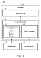
- FIG. 1 is a block diagram of a portable device 100 in accordance with an embodiment of the invention.
- the portable device 100 comprises a processing unit 110, a memory controller 120, a first memory 130, and a second memory 140.
- the processing unit 110 may access the first memory 120 and the second memory 130 via the memory controller 120.
- the processing unit 110 comprises one or more processors or other equivalent functional units or circuits.
- the processing unit 110 and the memory controller 120 can be integrated into an integrated circuit (IC) or an apparatus 190, e.g. a system-on-chip, and the first memory 130 and the second memory 140 are external to the apparatus 190.
- IC integrated circuit
- apparatus 190 e.g. a system-on-chip
- the first memory 130 may be a volatile memory (e.g. low-power DDR SDRAM) which has lower active power but has higher standby power than that of the second memory 140.
- the second memory 140 may be a non-volatile memory (e.g. magnetoresistive random-access memory (MRAM)) which does not need to refresh or less refresh time to keep data when the power to the second memory 140 is turned off, and the second memory has higher active power than that of the first memory 130.
- the memory controller 120 comprises a memory management circuit 121, and a direct memory access (DMA) controller 122, where the memory management circuit 121 comprises a buffer 123.
- the memory management circuit 121 is configured to control data access of both the first memory and the second memory.
- the buffer 123 may be an SRAM or a register file, but the invention is not limited thereto.
- FIG. 2A is a diagram of software-transparent memory accessing with hardware assistance in an active mode in accordance with an embodiment of the invention.
- the portable device 100 is in an active mode, and the processing unit 110 may access the first memory 130 or the second memory 140 through the memory controller 120.
- the processing unit 110 may build a software memory map 200 including a plurality of memory addresses (e.g. 211 ⁇ 213) and corresponding data (e.g. 221 ⁇ 213).
- the processing unit 110 may send a read or write command including a memory address to the memory controller 120, and the memory management circuit 121 of the memory controller 120 may analyze the memory address from the read or write command and determine that the first memory 130 or the second memory 140 is to be accessed.
- the memory management circuit 121 translates the memory address in the software memory map 200 from the processing unit 110 to a physical memory address which may correspond to the first memory 130 or the second memory 140.
- the frequently or repeatedly used data in the second memory 140 can be "migrated" (i.e. copied) to the first memory 130 to save power when the portable device 130 is in the active mode.
- the data in the second memory 140 which is less likely to be used in the active mode will not be migrated to the first memory 130 to reduce the overhead of data copying (i.e. data migration) between the first memory 130 and the second memory 140.
- the data 211 (“aaaa”), 222 (“bbbb”), and 223 (“cccc”) in the memory addresses 211, 212, and 213 of the software memory map 200 are directed to the physical memory address 214 of the first memory 130, the physical memory address 215 of the second memory 140, and the physical memory address 216 of the second memory 140, respectively.
- the memory management circuit 121 migrates the data 226 (“cccc") saved in the physical memory address 216 of the second memory 140 to the physical memory address 217 of the first memory 130, and thus the data 227 and 226 are identical at this time.
- the memory management circuit 121 changes the pointer of the software memory address 212 to direct to the physical memory address 217 of the first memory 130 from the physical memory address 216 of the second memory 140. Accordingly, the memory management circuit 121 may then access the data 227 "cccc" from the physical memory address 217 of the first memory 130 which has lower active power, and thus the power consumption of the portable device 100 can be reduced.
- the memory management circuit 121 records the dirty data information (i.e. physical memory address, pointer, etc.) of the dirty data between the first memory 130 and the second memory 140 in the buffer 123.
- FIG. 2B is a diagram of software-transparent memory accessing with hardware assistance in a sleep mode in accordance with an embodiment of the invention.
- the portable device 100 enters a sleep mode, the first memory 130 and the second memory 140 are turned off to save power. Specifically, before the portable device 100 enters a sleep mode, some of the currently used data stored in the first memory 130 should be migrated to the second memory 140 to prevent from data loss.
- the stored data in the first memory 130 are consistent with that in the second memory 140, no migration operation is performed.
- some pointers in the memory management circuit 121 are directed to the first memory 130 after data migration described in FIG. 2A .
- the pointers for memory addresses 211 and 212 in the software memory map 200 are directed to the physical memory addresses 214 and 217 of the first memory 130).
- the data in the corresponding physical memory address 217 of the first memory 130 may possibly be updated, such as the data 227 being updated to "dddd" which is different from the original data 226 "cccc" corresponding to the physical memory address 216 in the second memory 140.
- the DMA controller 122 directly accesses and migrates the data stored in the specific physical address of the first memory 130 to the corresponding physical memory address of the second memory 140 according to the dirty data information stored in the buffer 123.
- the data 226 is updated with the data 227 "dddd" in this case.
- the first memory 130 and the second memory 140 can be turned off to save power in the sleep mode.
- FIG. 2C is a diagram of software-transparent memory accessing with hardware assistance when waking up the portable device in accordance with an embodiment of the invention.
- the first memory 130 and the second memory 140 are both turned off, and the data that was previously used in the active mode is stored in the second memory 140 with "dirty data update".
- the portable device 100 is being awakened to the active mode, power to the first memory 130 and the second memory 140 is turned on, and the previously used data stored in the second memory 140 (e.g. data 225, 226 and 228) is directly retrieved by the processing unit 110 via the memory controller 120 to reduce the wake-up time.
- the first memory 130 is empty and there is no operation on the first memory 130 at this time.
- the portable device 100 is awakened to the active mode, and the memory controller 120 may migrate the frequently or repeatedly used data from the second memory 140 to the first memory 130, as described in the embodiment of FIG. 2A .
- FIG. 3 is a block diagram of the portable device in accordance with another embodiment of the invention.
- the memory management is performed by a software memory management unit 111 (e.g. a program code or firmware) executed by the processing unit 110.
- the memory management unit 111 may send different destination memory addresses to the first memory 130 and the second memory 140 to access the data stored in the first memory 130 and the second memory 140.
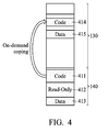
- FIG. 4 is a diagram of on-demand copying in the software memory management unit in accordance with an embodiment of the invention.
- the memory management unit 111 may copy the frequently or repeatedly used data and program code from the second memory 140 to the first memory 130.
- the memory management unit 111 copies the program code 411 and data 413 in the second memory 140 to the code 414 and data 415 in the first memory 130 when the portable device 100 is in the active mode.
- the memory management unit 111 also records the "dirty data information" when there is data conflict between the first memory 130 and the second memory 140.
- the memory management unit 111 determines whether dirty data exists between the first memory 130 and the second memory 140. If dirty data does exist, the memory management unit 111 copies the dirty data in the first memory 130 to the corresponding physical address in the second memory 140 via the DMA controller 122. The details are similar to the embodiment of FIG. 2B . Then, the first memory 130 and the second memory 140 can be turned off after the dirty data has been copied to the second memory 140. If dirty data does not exist, no migration is performed, and the first memory 130 and the second memory 140 can be turned off.
- the processing unit 111 When the portable device 100 is being awakened to the active mode from the sleep mode, the power to the first memory 130 and the second memory 140 is turned on, and the processing unit 111 directly retrieves the required system data stored in the second memory 140. It should be noted that the first memory 130 is empty and there is no operation with the first memory 130 at this time. After directly retrieving the system data stored in the second memory 140, the portable device 100 is awakened to the active mode, and the memory controller 120 may migrate the frequently or repeatedly used data from the second memory 140 to the first memory 130, as described in the embodiment of FIG. 2A .
- FIGs. 5A ⁇ 5C are diagrams illustrating power usage of different combinations of the first memory 130 and the second memory 140 in accordance with an embodiment of the invention.
- the power usage of the first memory 130 is shown in FIG. 5A .
- the first memory 130 is in the active mode and the active power of the first memory 130 is P1.
- the first memory 130 is in the sleep mode, and the retention power of the first memory 130 is P4, where P1 is larger than P4.
- the power usage of the second memory 140 is shown in FIG. 5B .
- the second memory 140 is in the active mode, and the active power of the second memory 140 is P2.
- the active power of the second memory 140 is higher than that of the first memory 130, and thus P2 is greater than P1.
- the second memory 140 is in the sleep mode, and the retention power of the second memory 140 is almost zero.
- the portable device 100 uses hybrid memory architecture in the first memory 130 and the second memory 140, and the hybrid memory architecture has the advantages of the first memory 130 and the second memory 140 being in the active mode and the sleep mode, respectively.
- the power usage of the hybrid memory architecture is shown in FIG. 5C .
- the hybrid memory architecture is in the active mode, and the frequently or repeatedly used data has been copied to the first memory 130 which has lower active power.
- the active power P5 of the hybrid memory architecture is slightly higher than the active power P1 of the first memory 130.
- the memory management circuit 121 copies the dirty data, that has data conflict between the first memory 130 and the second memory 140, from the first memory 130 to the second memory 140 according to the dirty data information stored in the buffer 123 via the DMA controller 122. Specifically, during the period between time t 1 and t 4 , the dirty data in the first memory 130 is backed up in the second memory 140, and the active power of the hybrid memory architecture is P3. Thus, the first memory 130 and the second memory 140 can be turned off at time t 4 , and the retention power of the hybrid memory architecture is approximately zero, like that of the second memory 140.
- FIG. 6 is an example of calculating power consumption of the hybrid memory architecture in accordance with an embodiment of the invention.
- the power consumption for a read command and a write command of the first memory 130 is 1 power unit
- the power consumption for a read command and a write command of the second memory 140 is 1.5 power units.
- Each of the first memory 130 and the second memory 140 has 16 blocks (e.g. block 0 ⁇ 15), where 64 bits of data can be stored in each block. It is assumed that four read operations are performed on blocks 0, 2, 4, and 6, and four write operations are performed on blocks 2 and 6. If prior suspend-to-storage technology and recovery-from-storage technologies are used in the portable device 100, there are 4x4 active read operations and 2x4 active write operations on the first memory 130.
- the DMA controller 122 When the portable device 100 is entering the sleep mode, all the data in each block of the first memory 130 are backed up to the second memory 140, and thus there are 16 read operations performed on the first memory 130 and 16 write operations performed on the second memory 140. In addition, when the portable device 100 is being awakened to the active mode, the DMA controller 122 first retrieves all the data stored in the second memory 140 and then writes the retrieved data into the first memory 130, thereby awakening the portable device 100 to the active mode. In other words, the processing unit 110 always reads the required data from the first memory 130 if prior techniques are used.
- the estimated power for the prior technologies in the scenario is 16x1 + 16*1.5 power units for system recovery, 16x1 + 8x1 power units for the active mode, and 16x1 + 16x1.5 power units for backing up data, and the total power is 104 power units.
- the hybrid memory architecture is used in the portable device 100, and it is assumed that the operating system of the portable device 100 can be recovered using the data in the blocks 0, 2, 4, and 6.
- the data in blocks 0, 2, 4, and 6 can be read from the second memory 140 once, and this data can be written into blocks 0, 2, 4, and 6 in the first memory for later use.
- the remaining three read operations on blocks 0, 2, 4, and 6, and four write operations on blocks 2 and 6 can be performed on the first memory 130 to save power.
- the data in blocks 2 and 6 are regarded as "dirty data" between the first memory 130 and the second memory 140 since four write operations are performed on blocks 2 and 6 in the first memory 130.
- the estimated power for the hybrid memory architecture in the scenario is 4x1 for system recovery, 12x1 + 8x1 + 4x1.5 for the active mode, and 2x1 + 2x1.5 for data backup, and the total power is 35 power units.
- the power unit in the aforementioned embodiment indicates power consumption, and can be measured in Watts, but the invention is not limited thereto. It should also be noted that the numeric values for the power consumption of the first memory 130 and the second memory 140 are for ease of description, and the invention is not limited thereto.
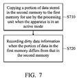
- FIG. 7 is a flow chart of a low-power memory-access method in an apparatus in accordance with an embodiment of the invention.
- step S710 a portion of data stored in the second memory 140 is copied to the first memory 130 for use by the processing unit 110 when the apparatus is in an active mode.
- step S720 dirty data information is recorded by the memory management circuit 121 when the portion of data in the first memory differs from that in the second memory. It should be noted that the recorded dirty data information is used to copy the dirty data from the first memory 130 to the second memory 140 when the apparatus 190 is entering the sleep mode. Thus, the number of memory access operations on the first memory 130 and the second memory 140 can be reduced.
- the processing unit 110 retrieves system data directly from the second memory 140 when the apparatus 190 is being awakened to the active mode from the sleep mode, thereby achieving fast waking-up of the apparatus 190.
Landscapes
- Engineering & Computer Science (AREA)
- Theoretical Computer Science (AREA)
- General Engineering & Computer Science (AREA)
- Physics & Mathematics (AREA)
- General Physics & Mathematics (AREA)
- Human Computer Interaction (AREA)
- Computer Hardware Design (AREA)
- Computing Systems (AREA)
- Computer Security & Cryptography (AREA)
- Power Sources (AREA)
- Techniques For Improving Reliability Of Storages (AREA)
Applications Claiming Priority (1)
| Application Number | Priority Date | Filing Date | Title |
|---|---|---|---|
| US14/848,872 US20170068304A1 (en) | 2015-09-09 | 2015-09-09 | Low-power memory-access method and associated apparatus |
Publications (1)
| Publication Number | Publication Date |
|---|---|
| EP3142015A1 true EP3142015A1 (fr) | 2017-03-15 |
Family
ID=56235607
Family Applications (1)
| Application Number | Title | Priority Date | Filing Date |
|---|---|---|---|
| EP16175228.2A Withdrawn EP3142015A1 (fr) | 2015-09-09 | 2016-06-20 | Procédé d'accès en mémoire de faible puissance et appareil associé |
Country Status (3)
| Country | Link |
|---|---|
| US (1) | US20170068304A1 (fr) |
| EP (1) | EP3142015A1 (fr) |
| CN (1) | CN107066068A (fr) |
Families Citing this family (8)
| Publication number | Priority date | Publication date | Assignee | Title |
|---|---|---|---|---|
| US11262921B2 (en) * | 2017-12-21 | 2022-03-01 | Qualcomm Incorporated | Partial area self refresh mode |
| US10860244B2 (en) * | 2017-12-26 | 2020-12-08 | Intel Corporation | Method and apparatus for multi-level memory early page demotion |
| US10884790B1 (en) * | 2018-05-02 | 2021-01-05 | Amazon Technologies, Inc. | Eliding redundant copying for virtual machine migration |
| US10768965B1 (en) | 2018-05-02 | 2020-09-08 | Amazon Technologies, Inc. | Reducing copy operations for a virtual machine migration |
| CN111512294A (zh) * | 2018-09-18 | 2020-08-07 | 华为技术有限公司 | 一种存储装置及电子设备 |
| US10860491B2 (en) | 2019-05-03 | 2020-12-08 | Mediate Inc. | Cache management method using object-oriented manner and associated microcontroller |
| CN121326232A (zh) * | 2021-02-09 | 2026-01-13 | 荣耀终端股份有限公司 | 一种数据读写方法和混合型存储器 |
| CN115359830B (zh) * | 2022-07-12 | 2024-03-08 | 浙江大学 | Scm介质存储模块的读方法写方法,以及存储控制器 |
Citations (7)
| Publication number | Priority date | Publication date | Assignee | Title |
|---|---|---|---|---|
| US20110296095A1 (en) * | 2010-05-25 | 2011-12-01 | Mediatek Inc. | Data movement engine and memory control methods thereof |
| WO2013095559A1 (fr) * | 2011-12-22 | 2013-06-27 | Intel Corporation | Economie d'énergie au moyen d'une fermeture de canal de mémoire |
| US20140013045A1 (en) * | 2011-12-29 | 2014-01-09 | James B. Crossland | Non-volatile ram disk |
| US20140068240A1 (en) * | 2012-08-30 | 2014-03-06 | Microsoft Corporation | Layout and execution of operating systems using bpram |
| US20140244960A1 (en) * | 2013-02-28 | 2014-08-28 | Kabushiki Kaisha Toshiba | Computing device, memory management method, and program |
| US20140304475A1 (en) * | 2011-12-20 | 2014-10-09 | Raj K Ramanujan | Dynamic partial power down of memory-side cache in a 2-level memory hierarchy |
| US20150012690A1 (en) * | 2013-03-15 | 2015-01-08 | Rolando H. Bruce | Multi-Leveled Cache Management in a Hybrid Storage System |
Family Cites Families (2)
| Publication number | Priority date | Publication date | Assignee | Title |
|---|---|---|---|---|
| EP1870814B1 (fr) * | 2006-06-19 | 2014-08-13 | Texas Instruments France | Procédé et dispositif pour pagination sécurisée pour dispositifs de microprocesseurs |
| KR20130033230A (ko) * | 2011-09-26 | 2013-04-03 | 삼성전자주식회사 | 하이브리드 메모리 장치, 이를 포함하는 시스템, 및 하이브리드 메모리장치의 데이터 기입 및 독출 방법 |
-
2015
- 2015-09-09 US US14/848,872 patent/US20170068304A1/en not_active Abandoned
-
2016
- 2016-06-20 EP EP16175228.2A patent/EP3142015A1/fr not_active Withdrawn
- 2016-09-09 CN CN201610813758.6A patent/CN107066068A/zh not_active Withdrawn
Patent Citations (7)
| Publication number | Priority date | Publication date | Assignee | Title |
|---|---|---|---|---|
| US20110296095A1 (en) * | 2010-05-25 | 2011-12-01 | Mediatek Inc. | Data movement engine and memory control methods thereof |
| US20140304475A1 (en) * | 2011-12-20 | 2014-10-09 | Raj K Ramanujan | Dynamic partial power down of memory-side cache in a 2-level memory hierarchy |
| WO2013095559A1 (fr) * | 2011-12-22 | 2013-06-27 | Intel Corporation | Economie d'énergie au moyen d'une fermeture de canal de mémoire |
| US20140013045A1 (en) * | 2011-12-29 | 2014-01-09 | James B. Crossland | Non-volatile ram disk |
| US20140068240A1 (en) * | 2012-08-30 | 2014-03-06 | Microsoft Corporation | Layout and execution of operating systems using bpram |
| US20140244960A1 (en) * | 2013-02-28 | 2014-08-28 | Kabushiki Kaisha Toshiba | Computing device, memory management method, and program |
| US20150012690A1 (en) * | 2013-03-15 | 2015-01-08 | Rolando H. Bruce | Multi-Leveled Cache Management in a Hybrid Storage System |
Also Published As
| Publication number | Publication date |
|---|---|
| CN107066068A (zh) | 2017-08-18 |
| US20170068304A1 (en) | 2017-03-09 |
Similar Documents
| Publication | Publication Date | Title |
|---|---|---|
| EP3142015A1 (fr) | Procédé d'accès en mémoire de faible puissance et appareil associé | |
| US7218566B1 (en) | Power management of memory via wake/sleep cycles | |
| TWI645334B (zh) | 用於管理操作狀態資料之方法、記憶體模組及主機裝置 | |
| TWI515747B (zh) | 用於動態記憶體功率管理之系統及方法 | |
| JP4969805B2 (ja) | 適応記憶システム | |
| US9032139B2 (en) | Memory allocation for fast platform hibernation and resumption of computing systems | |
| US8923088B2 (en) | Solid state storage device with sleep control circuit | |
| US9471130B2 (en) | Configuring idle states for entities in a computing device based on predictions of durations of idle periods | |
| JP6276470B2 (ja) | ポータブルコンピューティングデバイスの揮発性メモリのスタンバイ電力を低減するためのシステムおよび方法 | |
| US20120284475A1 (en) | Memory On-Demand, Managing Power In Memory | |
| US20150302930A1 (en) | Flash storage device with data integrity protection | |
| US11561715B2 (en) | Method and apparatus for presearching stored data | |
| CN103902013B (zh) | 存储器控制装置及方法 | |
| CN101118460A (zh) | 具有高功率和低功率处理器以及线程转移的系统 | |
| EP4020220B1 (fr) | Utilisation de tampon non-et pour la programmation de cellules multi-niveaux sans dram | |
| US9965017B2 (en) | System and method for conserving energy in non-volatile dual inline memory modules | |
| CN107369464B (zh) | 存储模块及包括其的系统 | |
| US10146483B2 (en) | Memory system | |
| US20110161647A1 (en) | Bootable volatile memory device, memory module and processing system comprising bootable volatile memory device, and method of booting processing system using bootable volatile memory device | |
| CN121569275A (zh) | 存储器自刷新功率门控 | |
| US8068373B1 (en) | Power management of memory via wake/sleep cycles | |
| CN112711548B (zh) | 内存装置、图像处理芯片以及内存控制方法 | |
| US20260003504A1 (en) | Power Gating for Memory Physical Layers | |
| US11334143B2 (en) | Processing system and control method wherein a microprocessor configured to set a plurality of memories into a self-refresh mode and a main processor in a standby mode | |
| CN105045370A (zh) | 在电子终端中执行睡眠状态管理的方法及其电子终端 |
Legal Events
| Date | Code | Title | Description |
|---|---|---|---|
| PUAI | Public reference made under article 153(3) epc to a published international application that has entered the european phase |
Free format text: ORIGINAL CODE: 0009012 |
|
| STAA | Information on the status of an ep patent application or granted ep patent |
Free format text: STATUS: THE APPLICATION HAS BEEN PUBLISHED |
|
| AK | Designated contracting states |
Kind code of ref document: A1 Designated state(s): AL AT BE BG CH CY CZ DE DK EE ES FI FR GB GR HR HU IE IS IT LI LT LU LV MC MK MT NL NO PL PT RO RS SE SI SK SM TR |
|
| AX | Request for extension of the european patent |
Extension state: BA ME |
|
| STAA | Information on the status of an ep patent application or granted ep patent |
Free format text: STATUS: REQUEST FOR EXAMINATION WAS MADE |
|
| 17P | Request for examination filed |
Effective date: 20170912 |
|
| RBV | Designated contracting states (corrected) |
Designated state(s): AL AT BE BG CH CY CZ DE DK EE ES FI FR GB GR HR HU IE IS IT LI LT LU LV MC MK MT NL NO PL PT RO RS SE SI SK SM TR |
|
| STAA | Information on the status of an ep patent application or granted ep patent |
Free format text: STATUS: EXAMINATION IS IN PROGRESS |
|
| 17Q | First examination report despatched |
Effective date: 20180206 |
|
| STAA | Information on the status of an ep patent application or granted ep patent |
Free format text: STATUS: THE APPLICATION HAS BEEN WITHDRAWN |
|
| 18W | Application withdrawn |
Effective date: 20180420 |