EP3142047A1 - Étiquette d'identification par radiofréquence passive, tête de lecture/écriture radiofréquence et système d'identification par radiofréquence - Google Patents
Étiquette d'identification par radiofréquence passive, tête de lecture/écriture radiofréquence et système d'identification par radiofréquence Download PDFInfo
- Publication number
- EP3142047A1 EP3142047A1 EP14892540.7A EP14892540A EP3142047A1 EP 3142047 A1 EP3142047 A1 EP 3142047A1 EP 14892540 A EP14892540 A EP 14892540A EP 3142047 A1 EP3142047 A1 EP 3142047A1
- Authority
- EP
- European Patent Office
- Prior art keywords
- read
- rfid tag
- passive rfid
- write head
- written
- Prior art date
- Legal status (The legal status is an assumption and is not a legal conclusion. Google has not performed a legal analysis and makes no representation as to the accuracy of the status listed.)
- Granted
Links
Images


Classifications
-
- G—PHYSICS
- G06—COMPUTING OR CALCULATING; COUNTING
- G06K—GRAPHICAL DATA READING; PRESENTATION OF DATA; RECORD CARRIERS; HANDLING RECORD CARRIERS
- G06K7/00—Methods or arrangements for sensing record carriers, e.g. for reading patterns
- G06K7/0008—General problems related to the reading of electronic memory record carriers, independent of its reading method, e.g. power transfer
-
- G—PHYSICS
- G06—COMPUTING OR CALCULATING; COUNTING
- G06K—GRAPHICAL DATA READING; PRESENTATION OF DATA; RECORD CARRIERS; HANDLING RECORD CARRIERS
- G06K17/00—Methods or arrangements for effecting co-operative working between equipments covered by two or more of main groups G06K1/00 - G06K15/00, e.g. automatic card files incorporating conveying and reading operations
-
- G—PHYSICS
- G06—COMPUTING OR CALCULATING; COUNTING
- G06K—GRAPHICAL DATA READING; PRESENTATION OF DATA; RECORD CARRIERS; HANDLING RECORD CARRIERS
- G06K19/00—Record carriers for use with machines and with at least a part designed to carry digital markings
- G06K19/06—Record carriers for use with machines and with at least a part designed to carry digital markings characterised by the kind of the digital marking, e.g. shape, nature, code
- G06K19/067—Record carriers with conductive marks, printed circuits or semiconductor circuit elements, e.g. credit or identity cards also with resonating or responding marks without active components
- G06K19/07—Record carriers with conductive marks, printed circuits or semiconductor circuit elements, e.g. credit or identity cards also with resonating or responding marks without active components with integrated circuit chips
- G06K19/0701—Record carriers with conductive marks, printed circuits or semiconductor circuit elements, e.g. credit or identity cards also with resonating or responding marks without active components with integrated circuit chips at least one of the integrated circuit chips comprising an arrangement for power management
- G06K19/0707—Record carriers with conductive marks, printed circuits or semiconductor circuit elements, e.g. credit or identity cards also with resonating or responding marks without active components with integrated circuit chips at least one of the integrated circuit chips comprising an arrangement for power management the arrangement being capable of collecting energy from external energy sources, e.g. thermocouples, vibration, electromagnetic radiation
-
- G—PHYSICS
- G06—COMPUTING OR CALCULATING; COUNTING
- G06K—GRAPHICAL DATA READING; PRESENTATION OF DATA; RECORD CARRIERS; HANDLING RECORD CARRIERS
- G06K19/00—Record carriers for use with machines and with at least a part designed to carry digital markings
- G06K19/06—Record carriers for use with machines and with at least a part designed to carry digital markings characterised by the kind of the digital marking, e.g. shape, nature, code
- G06K19/067—Record carriers with conductive marks, printed circuits or semiconductor circuit elements, e.g. credit or identity cards also with resonating or responding marks without active components
- G06K19/07—Record carriers with conductive marks, printed circuits or semiconductor circuit elements, e.g. credit or identity cards also with resonating or responding marks without active components with integrated circuit chips
- G06K19/0723—Record carriers with conductive marks, printed circuits or semiconductor circuit elements, e.g. credit or identity cards also with resonating or responding marks without active components with integrated circuit chips the record carrier comprising an arrangement for non-contact communication, e.g. wireless communication circuits on transponder cards, non-contact smart cards or RFIDs
-
- G—PHYSICS
- G06—COMPUTING OR CALCULATING; COUNTING
- G06K—GRAPHICAL DATA READING; PRESENTATION OF DATA; RECORD CARRIERS; HANDLING RECORD CARRIERS
- G06K7/00—Methods or arrangements for sensing record carriers, e.g. for reading patterns
- G06K7/10—Methods or arrangements for sensing record carriers, e.g. for reading patterns by electromagnetic radiation, e.g. optical sensing; by corpuscular radiation
- G06K7/10009—Methods or arrangements for sensing record carriers, e.g. for reading patterns by electromagnetic radiation, e.g. optical sensing; by corpuscular radiation sensing by radiation using wavelengths larger than 0.1 mm, e.g. radio-waves or microwaves
Definitions
- the present invention relates to the field of communications, and in particular relates to a passive radio frequency identification (RFID) tag, a radio frequency (RF) read/write head and an RFID system.
- RFID radio frequency identification
- RF radio frequency
- an optical fiber network has replaced a copper wire communication network, and the optical fiber network nearly covers all communication networks from a core network and a bearer network to an access network and then a fiber to the home (FTTH).
- FTTH fiber to the home
- an intelligent tag is added to each optical connection point, then a read/write head automatically reads the tag, and relevant data are reported to a network manager, so that detection automation of the optical fiber connection points gradually becomes a consensus, thereby realizing a visible and manageable optical fiber network.
- ODN intelligent optical distribution network
- a tag and a read/write head are added to each optical connection head, so as to enable the intelligent ODN to automatically report a connection state of the intelligent ODN, i.e., intelligentization.
- CCSA China Communications Standards Association
- CCSA has formulated a series of corresponding standards for the intelligent ODN, and a corresponding industrial chain begins to form.
- a contact-type tag technology typically includes 1-Wire interface or an Electrically Erasable Programmable Read-only Memory (EEPROM) interface.
- EEPROM Electrically Erasable Programmable Read-only Memory
- a tag needs to be powered.
- the contact-type tag technology proposes higher requirements for structural design and reliability of the tag. Meanwhile, the contact-type tag technology is not flexible enough due to physical connection in some rebuilding scenes.
- the other of the technologies is a non-contact-type tag technology, which typically includes an RFID technology. As shown in Fig.
- a coil of the RFID technology is required to have a certain working area so as to generate enough induction current for driving a chip to work normally.
- a working coil of the read/write head is also required to have a certain working area, causing that adjacent RFIDs are also induced and causing mutual interference. Therefore, this technology is unsuitable for a working environment with optical nodes of dense optical fiber connection heads.
- a read/write technology is required so that a tag can not only maintain non-contact-type read/write, but also meet other tags required by optical nodes of dense optical fiber connection heads.
- Embodiments of the present invention provide a passive RFID tag, an RF read/write head and an RFID system, so as to at least solve the problem that a contact-type tag technology and RFID tags can not meet the requirements for dense scenes in relevant technologies.
- an RF read/write head including: a plurality of optical transmitters, a chip and an RF antenna, where the RF antenna is connected with the chip; the plurality of optical transmitters are connected with the chip; and the chip is configured to control an optical transmitter corresponding to a designated RFID tag in the plurality of optical transmitters to emit light so as to start the designated RFID tag when a read/write operation is carried out on the designated RFID tag in the plurality of RFID tags; and carry out the read/write operation on the designated RFID tag.
- the RF read/write head includes one RF antenna.
- each of the optical transmitters is a light emitting diode (LED).
- LED light emitting diode
- a passive RFID tag including: an optical to electrical converter (OEC), an RF antenna and a chip, where the OEC is connected with the chip and the RF antenna and is configured to convert optical energy transmitted by an RF read/write head into electrical energy and supply power to the chip and the RF antenna; the RF antenna is connected with the chip; and the chip is configured to store tag information and respond to a read/write operation of the RF read/write head.
- OEC optical to electrical converter
- RF antenna is connected with the chip
- the chip is configured to store tag information and respond to a read/write operation of the RF read/write head.
- an RF tag identification system including a plurality of passive RFID tags and an RF read/write head, where each of the passive RFID tag includes: an OEC, a first RF antenna and a first chip, where the OEC is connected with the first chip and the first RF antenna and is configured to convert optical energy transmitted by the RF read/write head into electrical energy and supply power to the first chip and the first RF antenna; and the first chip is configured to store tag information and respond to a read/write operation of the RF read/write head; the RF read/write head includes: a plurality of optical transmitters, a second chip and a second RF antenna, where the second RF antenna is connected with the second chip; the plurality of optical transmitters are connected with the second chip; and the second chip is configured to control an optical transmitter corresponding to a designated RFID tag in the plurality of optical transmitters to emit light so as to start the designated RFID tag when a read/write operation is carried out on the designated RFID tag in the plurality of RFID
- the RF read/write head includes one second RF antenna.
- each of the optical transmitters is an LED.
- an optical fiber connection head is provided, and the optical fiber connection head is provided with the above passive RFID tags of the present invention.
- an optical fiber wiring apparatus is provided, and the optical fiber wiring apparatus is provided with the above RF read/write head of the present invention, where the wiring apparatus includes a plurality of connection ports, and each connection port is configured to be connected with the above optical fiber connection head of the present invention in a pluggable manner; and a plurality of optical transmitters of the RF read/write head are arranged at positions that the optical transmitters are respectively in alignment to the corresponding passive RFID tags on the optical fiber connection heads when the plurality of optical fiber connection heads are inserted into the plurality of connection ports.
- a read/write method of an RFID tag system includes: the above RF read/write head of the present invention and the plurality of above passive RFID tags of the present invention.
- the method includes: determining the passive RFID tag currently read and written; controlling the optical transmitter corresponding to the passive RFID tag currently read and written in the RF read/write head to emit light, so as to supply power to the passive RFID tag currently read and written; and carrying out a read/write operation on the passive RFID tag currently read and written.
- the carrying out the read/write operation on the passive RFID tag currently read and written includes: sending an inquiry instruction to the passive RFID tag currently read and written, where the inquiry instruction is configured to inquire a state of the passive RFID tag currently read and written; and receiving a first state sent by the passive RFID tag currently read and written.
- the above method further includes: judging the first state; and distributing tag information to the passive RFID tag currently read and written when the first state indicates that the passive RFID tag currently read and written is blank.
- the above method further includes: judging the first state; and requesting the passive RFID tag currently read and written to report its tag information when the first state indicates that the passive RFID tag currently read and written has the tag information.
- the above method further includes: receiving the tag information reported by the passive RFID tag currently read and written; judging whether the received tag information meets a preset condition; and distributing new tag information to the passive RFID tag currently read and written when the received tag information does not meet the preset condition.
- the method further includes: closing an optical transmitter corresponding to the passive RFID tag currently read and written in the RF read/write head; and carrying out read/write operations on other passive RFID tags in the plurality of passive RFID tags.
- a read/write apparatus of an RFID tag system includes the above RF read/write head of the present invention and the plurality of above passive RFID tags of the present invention.
- the apparatus includes: a determination module, configured to determine the passive RFID tag currently read and written; a control module, configured to control an optical transmitter corresponding to the passive RFID tag currently read and written in the RF read/write head to emit light, so as to supply power to the passive RFID tag currently read and written; and a read/write module, configured to carry out a read/write operation on the passive RFID tag currently read and written.
- non-contact-type RFID is realized, and mutual interference of the RFID tags in dense scenes is reduced or avoided.
- the following embodiments provide a non-contact-type tag solution, where RFID tags are charged by a technology of an OEC, and an RFID tag with the OEC is called as an optical RFID tag for short and also called as a passive RFID tag.
- Fig. 3 is a structural block diagram illustrating an RF read/write head according to embodiments of the present invention.
- the RF read/write head of embodiments of the present invention may include: a plurality of optical transmitters 310, a chip 320 and an RF antenna 330, where the RF antenna 330 is connected with the chip 320; the plurality of optical transmitters 310 are connected with the chip 320; and the chip 320 is configured to control an optical transmitter 310 corresponding to a designated RFID tag in the plurality of optical transmitters 310 to emit light so as to start the designated RFID tag when a read/write operation is carried out on the designated RFID tag in a plurality of RFID tags, and is also configured to carry out a read/write operation on the designated RFID tag.
- the RF read/write head may include only one RF antenna 330. Through the preferable implementation manner, it is unnecessary to set one RF antenna for each RFID tag, so that cost is reduced.
- a plurality of RF antennas 330 may be arranged; and, in order to avoid mutual interference, a certain distance is preferably kept among the plurality of RF antennas 330.
- the optical transmitters 310 may be LEDs, but not limited thereto.
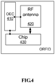
- Fig. 4 is a structural block diagram illustrating a passive RFID tag according to embodiments of the present invention.
- the passive RFID tag of embodiments of the present invention mainly includes: an OEC 410, an RF antenna 420 and a chip 430, where the OEC 410 is connected with the chip 430 and the RF antenna 420 and is configured to convert optical energy transmitted by an RF read/write head into electrical energy and supply power to the chip 430 and the RF antenna 420; the RF antenna 420 is connected with the chip 430; and the chip 430 is configured to store tag information and respond to a read/write operation of the RF read/write head.
- Fig. 5 is a schematic diagram illustrating an RF tag identification system according to embodiments of the present invention.
- the system includes: a plurality of passive RFID tags 1 and an RF read/write head 2, where with reference to Fig. 4 , each passive RFID tag 1 includes: an OEC, an RF antenna and a chip, where the OEC is connected with the chip and the RF antenna and is configured to convert optical energy transmitted by the RF read/write head into electrical energy and supply power to the chip and the RF antenna; and the chip is configured to store tag information and respond to a read/write operation of the RF read/write head 2; and with reference to Fig.
- the RF read/write head includes: a plurality of optical transmitters, a chip and an RF antenna, where the RF antenna is connected with the chip; the plurality of optical transmitters are connected with the chip; and the chip is configured to control an optical transmitter corresponding to a designated RFID tag in the plurality of optical transmitters to emit light so as to start the designated RFID tag when a read/write operation is carried out on the designated RFID tag in the plurality of RFID tags; and is also configured to carry out the read/write operation on the designated RFID tag.
- the RF read/write head 2 may include only one RF antenna.
- the optical transmitter may be an LED, but not limited thereto.
- the passive RFID tags 1 and the RF read/write head 2 are as described with reference to embodiment I and embodiment II and are not repeated here.
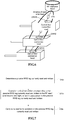
- Fig. 6 is a schematic diagram illustrating optical fiber connection heads and an optical fiber wiring apparatus according to embodiments of the present invention.
- each optical fiber connection head is provided with a passive RFID tag of embodiment II.
- the optical fiber wiring apparatus is provided with an RF read/write head of embodiment I, where the wiring apparatus includes a plurality of connection ports, each of which is configured to be connected with the optical fiber connection head in a pluggable manner; and a plurality of optical transmitters of the RFID head are arranged at positions that the optical fiber connection heads are respectively in alignment to the corresponding passive RFID tags on the optical fiber connection heads when the plurality of optical fiber connection heads are inserted into the plurality of connection ports.
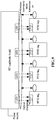
- Fig. 7 is a flow chart illustrating a read/write method of an RFID tag system according to embodiments of the present invention.
- the RFID tag system includes an RF read/write head of embodiment I and a plurality of passive RFID tags of embodiment II. As shown in Fig. 7 , the method includes step S702 to step S706.
- step S702 a passive RFID tag currently read and written is determined.
- step S704 an optical transmitter corresponding to the passive RFID tag currently read and written in the RF read/write head is controlled to emit light, so as to supply power to the passive RFID tag currently read and written.
- step S706 a read/write operation is carried out on the passive RFID tag currently read and written.
- the above step S706 may include: sending an inquiry instruction to the passive RFID tag currently read and written, where the inquiry instruction is configured to inquire a state of the passive RFID tag currently read and written; and receiving a first state sent by the passive RFID tag currently read and written.
- the above state may be tag information and the like.
- the tag information may include identity information and position information.
- the method may further include: judging the above first state; and distributing tag information to the passive RFID tag currently read and written when the first state indicates that the passive RFID tag currently read and written is blank.
- the method may further include: judging the above first state; and requesting the passive RFID tag currently read and written to report its tag information when the first state indicates that the passive RFID tag currently read and written has tag information.
- the method may further include: receiving tag information reported by the passive RFID tag currently read and written; judging whether the received tag information meets a preset condition; and distributing new tag information to the passive RFID tag currently read and written when the received tag information does not meet the preset condition.
- the method may further include: closing the optical transmitter corresponding to the passive RFID tag currently read and written in the RF read/write head; and carrying out read/write operations on other passive RFID tags in the plurality of passive RFID tags.
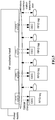
- Fig. 8 is a structural block diagram illustrating a read/write apparatus of an RFID tag system according to embodiments of the present invention.
- the apparatus includes: a determination module 810, configured to determine a passive RFID tag currently read and written; a control module 820, configured to control an optical transmitter corresponding to the passive RFID tag currently read and written in the RF read/write head to emit light so as to supply power to the passive RFID tag currently read and written; and a read/write module 830, configured to carry out a read/write operation on the passive RFID tag currently read and written.
- Fig. 9 is a schematic diagram illustrating a preferable RFID system according to embodiments of the present invention. As shown in Fig. 9 , the system includes: an RF read/write head and a plurality of passive RFID tags.
- the RF read/write head is composed of a plurality of optical transmitters, an RF antenna and a control chip.
- the RF read/write head is an active device, may transmit light through the optical transmitters to charge the passive RFID tags and may also transmit RF signals to the passive RFID tags so as to transmit instructions; the RF antenna of the RF read/write head may also be configured to receive data signals transmitted back from the passive RFID tags, and the control chip processes the data signals.
- a sequence that the tags receive and transmit the information is controlled by controlling transmission states of the optical transmitters (which are LEDs in the preferable implementation manner), namely, if information of a certain designated tag needs to be read and written, a corresponding optical transmitter above the corresponding tag is started so as to charge the tag; and, the optical transmitter is closed after the read/write operation is completed, while other tags are in a no power state as other optical transmitters are closed. Therefore, the other tags cannot receive or transmit signals.
- the optical transmitters which are LEDs in the preferable implementation manner
- All the passive RFID tags share one RF antenna of the RF read/write head, while a control part and a processing part (including the chip) of the RF read/write head are arranged at idle positions beside the RF antenna.
- One advantage of doing this is that there is no need to arrange a complete read/write head on each tag, thereby reducing cost and reducing technical difficulty in reducing volume of the RF read/write head; and a corresponding LED may be arranged in a space above the narrow tag, and the tags share one RF antenna, thereby reducing cost and installation difficulty.
- the passive RFID tag includes an OEC, an RF antenna and a chip.
- the OEC converts received optical energy into electrical energy and transmits the electrical energy to the RF antenna and the chip
- the RF antenna transmits a received signal to the chip
- the RF antenna is started as required to transmit a reply signal to the RF read/write head after the chip processes data.
- the passive RFID tags are passive, firstly, the RF read/write head emits light to charge the passive RFID tags; then the RF read/write head sends corresponding instructions to the passive RFID tags; the passive RFID tags transmit corresponding replies by own RF antenna after receiving the instructions; and the read/write head processes the replies after receiving them.
- the read/write head informs the passive RFID tags of having received and ending if information is sufficient; and if the information is insufficient, the read/write head further sends inquiry instructions, and the passive RFID tags further send replies as required, and the process would not stop until the read/write head is satisfied.
- the read/write head is in non-contact with the passive RFID tags, but a distance between the read/write head and the passive RFID tags is very short and is generally limited to be very short. The distance may be limited to be within 1 cm in an application in an intelligent ODN, and data transmission between the read/write head and the passive RFID tags is realized through a video wireless communication point-to-point (P2P) technology.
- P2P video wireless communication point
- read/write for tag information is initiated by a chip in an RF read/write head.
- Passive RFID tags mainly store identity information and position information. These information are assigned by the RF read/write head and may also be modified by the RF read/write head.
- a working power supply of the passive RFID tags comes from their OECs by optical conversion, the passive RFID tags are charged by the RF read/write head, and the RF read/write head can control a starting or closing state of optical transmitters above the passive RFID tags so as to determine corresponding tags to read information.
- the RF read/write head is an active device and includes a plurality of optical transmitters, an RF antenna and a chip, where the optical transmitters are generally LEDs and have an effect of charging the passive RFID tags.
- the RF antenna has an effect of transmitting instructions to the passive RFID tags, and receiving signals sent by the passive RFID tags.
- the chip may receive an instruction of an external network manager, start read/write for the passive RFID tags, assign identity information and position information to blank passive RFID tags, read and compare passive RFID tags already have identity information, and modify corresponding information for the passive RFID tags.
- the control chip may start information transmission and reading for a certain passive RFID tag according to a starting or closing state of the LED, and finally, the read/write head transmits relevant information to the network manager or a control center for storing.
- the passive RFID tag is passive and includes an OEC, an RF antenna and a chip, where the OEC receives light of the RF read/write head and converts the light into a power supply to be used by the RF antenna and the chip; the RF antenna converts the received instruction of the RF read/write head into an electrical signal and transmits the electrical signal to the chip; and the chip can process the instruction and start the RF antenna to reply; the RF antenna sends a reply signal according to requirements of the chip, and meanwhile, the chip has a function of information storing.
- the OEC receives light of the RF read/write head and converts the light into a power supply to be used by the RF antenna and the chip
- the RF antenna converts the received instruction of the RF read/write head into an electrical signal and transmits the electrical signal to the chip
- the chip can process the instruction and start the RF antenna to reply; the RF antenna sends a reply signal according to requirements of the chip, and meanwhile, the chip has a function of information storing
- passive RFID tags are arranged on optical fiber connection heads.
- Corresponding LED optical transmitters are arranged above the tags, while a control part and a processing part (including a chip and the like) of an RF read/write head are arranged at idle positions of a device, and all the tags share one RF antenna of the RF read/write head. It indicates that an optical fiber is already in a connection state when the optical fiber connection heads are inserted into a connecting box, and at this moment, the tags are just below the optical transmitters of the RF read/write head.
- the read/write head receives an instruction of a network manager or a control center and carries out read/write on the tag, and the chip starts a read/write process, in which firstly the read/write head opens the LED corresponding to the passive RFID tag to charge the passive RFID tag, and then following test steps are started to be executed.
- step 1 an inquiry instruction, such as a state of the tag, is transmitted to the passive RFID tag.
- step 2 the passive RFID tag replies a current state, such as a blank state or a state of having identity information.
- step 3 the read/write head distributes one piece of identity information to the passive RFID tag if the tag has blank identity information; and the read/write head requires the passive RFID tag to report identity information if the passive RFID tag has right identity information.
- step 4 the passive RFID tag reports own current identity information after completing the execution.
- step 5 the read/write head verifies the identity information, and re-assigns new identity information to the passive RFID tag if the identity information does not meet requirements; the passive RFID tag repeats step 4; the read/write head re-assesses the information, and steps 3, 4 and 5 are repeated if the read/write head is not satisfied; and the read/write head sends an instruction of ending if information fed back meets requirements.
- step 6 the passive RFID tag replies ending and confirmation after receiving the ending instruction.
- step 7 the read/write head closes the LED after receiving the reply; and in step 8, the read/write head opens an LED corresponding to another passive RFID tag, and steps 1-7 are repeated.
- the RF antenna of the passive RFID tag does not need to consider the problem of power supply. Therefore, the function of the antenna recovers to the RF transmitting and receiving instincts; the antenna can be designed to be smaller, thereby greatly reducing the size and the volume of the tag; the size of the corresponding RF read/write head may also not need to be considered; only one LED optical transmitter needs to be arranged above the tag; meanwhile, the RF antenna and other parts are used in common, thereby greatly reducing the cost and overcoming the problem of limiting an application of the pure RFID as the pure RFID cannot be made to be small; and the passive RFID tag can solve the problem of identification of the dense optical connection heads.
- the read/write head can emit light to charge the tag only when the read/write head carries out read/write. In this way, the problem of supplying power by mistake to the adjacent tags does not exist, while the adjacent tags do not have enough power to support signal reception and transmission due to no irradiation of the light, therefore, the possibility of misjudgment of the read/write head as adjacent pure RFID tags compete to send signals is also avoided.
- all the above modules or steps of the present invention may be realized by a universal calculating apparatus and may be centralized on a single calculating apparatus or may be distributed on a network formed by a plurality of calculating apparatus.
- all the above modules or steps of the present invention may be realized by an executable program code of the calculating apparatus, so that all the above modules or steps of the present invention may be stored in a storing apparatus and then executed by the calculating apparatus.
- the shown or described steps may be executed according to a sequence different from the sequence here, or steps are respectively made into a plurality of integrated circuit modules, or a plurality of modules or steps in all the above modules or steps are made into a single integrated circuit module to realize. In this way, the present invention is not limited to a combination of any specific hardware and software.
- the passive RFID tag, the RF read/write head and the RFID system have following beneficial effects: firstly, the RF antenna of the passive RFID tag does not need to consider the problem of power supply, and the antenna can be designed to be smaller, thereby greatly reducing the size and the volume of the tag; the size of the corresponding RF read/write head may also not need to be considered; only one LED optical transmitter needs to be arranged above the tag; and meanwhile, the RF antenna and other parts are shared, thereby greatly reducing the cost.
- the passive RFID tag can solve the problem of identification of the dense optical connection heads.
- the read/write head can emit light to charge the tag only when the read/write head carries out read/write. In this way, the problem of supplying power by mistake to the adjacent tags does not exist, while the adjacent tags do not have enough power to support signal reception and transmission due to no irradiation of the light, therefore, the possibility of misjudgment of the read/write head as adjacent pure RFID tags compete to send signals is also avoided.
Landscapes
- Engineering & Computer Science (AREA)
- Physics & Mathematics (AREA)
- General Physics & Mathematics (AREA)
- Theoretical Computer Science (AREA)
- Microelectronics & Electronic Packaging (AREA)
- Computer Hardware Design (AREA)
- Electromagnetism (AREA)
- Computer Vision & Pattern Recognition (AREA)
- Artificial Intelligence (AREA)
- Health & Medical Sciences (AREA)
- Toxicology (AREA)
- General Health & Medical Sciences (AREA)
- Computer Networks & Wireless Communication (AREA)
- Near-Field Transmission Systems (AREA)
Applications Claiming Priority (2)
| Application Number | Priority Date | Filing Date | Title |
|---|---|---|---|
| CN201410223544.4A CN105095928A (zh) | 2014-05-23 | 2014-05-23 | 无源射频识别标签、射频读写头及射频识别系统 |
| PCT/CN2014/091810 WO2015176514A1 (fr) | 2014-05-23 | 2014-11-20 | Étiquette d'identification par radiofréquence passive, tête de lecture/écriture radiofréquence et système d'identification par radiofréquence |
Publications (3)
| Publication Number | Publication Date |
|---|---|
| EP3142047A1 true EP3142047A1 (fr) | 2017-03-15 |
| EP3142047A4 EP3142047A4 (fr) | 2018-02-21 |
| EP3142047B1 EP3142047B1 (fr) | 2019-08-21 |
Family
ID=54553368
Family Applications (1)
| Application Number | Title | Priority Date | Filing Date |
|---|---|---|---|
| EP14892540.7A Active EP3142047B1 (fr) | 2014-05-23 | 2014-11-20 | Étiquette d'identification par radiofréquence passive, tête de lecture/écriture radiofréquence et système d'identification par radiofréquence |
Country Status (3)
| Country | Link |
|---|---|
| EP (1) | EP3142047B1 (fr) |
| CN (1) | CN105095928A (fr) |
| WO (1) | WO2015176514A1 (fr) |
Cited By (1)
| Publication number | Priority date | Publication date | Assignee | Title |
|---|---|---|---|---|
| US12182651B2 (en) | 2019-08-20 | 2024-12-31 | Avery Dennison Retail Information Services Llc | RFID read and write power setting system and method |
Families Citing this family (3)
| Publication number | Priority date | Publication date | Assignee | Title |
|---|---|---|---|---|
| CN108702035A (zh) * | 2016-01-08 | 2018-10-23 | 泰斯尼克斯公司 | 对远程射频识别标签进行充电 |
| CN108234024A (zh) * | 2016-12-21 | 2018-06-29 | 中兴通讯股份有限公司 | Odn系统及其工作方法 |
| US11192055B2 (en) | 2017-08-30 | 2021-12-07 | Cummins Filtration Ip, Inc. | Interlock for genuine filter recognition |
Family Cites Families (7)
| Publication number | Priority date | Publication date | Assignee | Title |
|---|---|---|---|---|
| AU2001275117A1 (en) * | 2000-06-06 | 2001-12-17 | Battelle Memorial Institute | Remote communication system and method |
| GB2410151A (en) * | 2004-01-15 | 2005-07-20 | Rf Tags Ltd | A radio frequency identification tag with means sensitive to light for controlling communication between rfid tag and reader |
| KR100936893B1 (ko) * | 2008-01-04 | 2010-01-14 | 중앙대학교 산학협력단 | 태그 인식 방법, 충돌 방지 방법 및 이를 이용한 rfid태그 |
| JP5094979B2 (ja) * | 2008-03-12 | 2012-12-12 | エレクトロニクス アンド テレコミュニケーションズ リサーチ インスチチュート | 衝突状況に応じて命令を再伝送するrfidリーダー装置及びその制御方法 |
| CN101533460A (zh) * | 2009-04-24 | 2009-09-16 | 清华大学 | 一种射频识别的系统和方法 |
| CN104350508A (zh) * | 2012-03-30 | 2015-02-11 | 泰科电子英国有限公司 | Rfid读取器扩展器 |
| CN103488967B (zh) * | 2013-10-14 | 2016-08-10 | 张祖锋 | 一种基于可见光或红外定位的机柜管理系统及方法 |
-
2014
- 2014-05-23 CN CN201410223544.4A patent/CN105095928A/zh active Pending
- 2014-11-20 EP EP14892540.7A patent/EP3142047B1/fr active Active
- 2014-11-20 WO PCT/CN2014/091810 patent/WO2015176514A1/fr not_active Ceased
Cited By (1)
| Publication number | Priority date | Publication date | Assignee | Title |
|---|---|---|---|---|
| US12182651B2 (en) | 2019-08-20 | 2024-12-31 | Avery Dennison Retail Information Services Llc | RFID read and write power setting system and method |
Also Published As
| Publication number | Publication date |
|---|---|
| EP3142047B1 (fr) | 2019-08-21 |
| WO2015176514A1 (fr) | 2015-11-26 |
| EP3142047A4 (fr) | 2018-02-21 |
| CN105095928A (zh) | 2015-11-25 |
Similar Documents
| Publication | Publication Date | Title |
|---|---|---|
| US20170116441A1 (en) | Passive optical tag, optical read/write device and intelligent optical distribution network | |
| CN105095929A (zh) | 无源射频识别标签、光学射频读写头及射频识别系统 | |
| EP3142047B1 (fr) | Étiquette d'identification par radiofréquence passive, tête de lecture/écriture radiofréquence et système d'identification par radiofréquence | |
| EP3147813A1 (fr) | Étiquette optique passive du type à réflexion, dispositif de lecture/écriture optique et réseau de distribution optique intelligent | |
| CN101647028B (zh) | 在自动化组件和移动操作终端之间建立无线通信连接的方法 | |
| CN102819518A (zh) | 一种射频识别总线系统 | |
| CN113965919B (zh) | 信息检测方法及基站 | |
| WO2019033885A1 (fr) | Procédé de gestion de support, terminal de gestion, appareil, système et support de stockage | |
| US12229063B2 (en) | Method of storing instructions in program memory and associated system | |
| CN103116734A (zh) | Rfid系统基于功率控制的防碰撞方法 | |
| CN114925788A (zh) | 一种标签定位方法以及相关设备 | |
| US20150053758A1 (en) | Fiber management system and method thereof | |
| EP1933260B1 (fr) | Système et procédé de surveillance à base de RFID | |
| US20070175995A1 (en) | RFID reader/writer | |
| CN105357664A (zh) | 一种无线控制系统及其数据通信方法 | |
| CN110490016A (zh) | 一种无线射频识别系统 | |
| CN107886019B (zh) | 级联设备和天线级联系统 | |
| CN108172964B (zh) | 一种具有标识功能的室分天线 | |
| US8872630B2 (en) | Method and apparatus for cabinet asset management, and cabinet system | |
| WO2016150280A1 (fr) | Étiquette opto-électronique passive, lecteur-scripteur opto-électronique et système d'identification opto-électronique passif | |
| US9633240B2 (en) | RFID reader/writer device | |
| CN118646969A (zh) | 一种无源物联通信系统 | |
| CN201540583U (zh) | Rfid智能天线 | |
| CN1897017B (zh) | 用于设置在通信网络中的现场工作站的参数的方法和系统 | |
| CN108960388A (zh) | 一种连接检测系统及方法 |
Legal Events
| Date | Code | Title | Description |
|---|---|---|---|
| STAA | Information on the status of an ep patent application or granted ep patent |
Free format text: STATUS: THE INTERNATIONAL PUBLICATION HAS BEEN MADE |
|
| PUAI | Public reference made under article 153(3) epc to a published international application that has entered the european phase |
Free format text: ORIGINAL CODE: 0009012 |
|
| STAA | Information on the status of an ep patent application or granted ep patent |
Free format text: STATUS: REQUEST FOR EXAMINATION WAS MADE |
|
| 17P | Request for examination filed |
Effective date: 20161209 |
|
| AK | Designated contracting states |
Kind code of ref document: A1 Designated state(s): AL AT BE BG CH CY CZ DE DK EE ES FI FR GB GR HR HU IE IS IT LI LT LU LV MC MK MT NL NO PL PT RO RS SE SI SK SM TR |
|
| AX | Request for extension of the european patent |
Extension state: BA ME |
|
| DAX | Request for extension of the european patent (deleted) | ||
| A4 | Supplementary search report drawn up and despatched |
Effective date: 20180123 |
|
| RIC1 | Information provided on ipc code assigned before grant |
Ipc: G06K 17/00 20060101AFI20180117BHEP Ipc: G06K 7/00 20060101ALI20180117BHEP Ipc: G06K 7/10 20060101ALI20180117BHEP Ipc: G06K 19/07 20060101ALI20180117BHEP |
|
| GRAP | Despatch of communication of intention to grant a patent |
Free format text: ORIGINAL CODE: EPIDOSNIGR1 |
|
| STAA | Information on the status of an ep patent application or granted ep patent |
Free format text: STATUS: GRANT OF PATENT IS INTENDED |
|
| RIC1 | Information provided on ipc code assigned before grant |
Ipc: G06K 7/10 20060101ALI20190314BHEP Ipc: G06K 19/07 20060101ALI20190314BHEP Ipc: G06K 17/00 20060101AFI20190314BHEP Ipc: G06K 7/00 20060101ALI20190314BHEP |
|
| INTG | Intention to grant announced |
Effective date: 20190401 |
|
| GRAS | Grant fee paid |
Free format text: ORIGINAL CODE: EPIDOSNIGR3 |
|
| GRAA | (expected) grant |
Free format text: ORIGINAL CODE: 0009210 |
|
| STAA | Information on the status of an ep patent application or granted ep patent |
Free format text: STATUS: THE PATENT HAS BEEN GRANTED |
|
| AK | Designated contracting states |
Kind code of ref document: B1 Designated state(s): AL AT BE BG CH CY CZ DE DK EE ES FI FR GB GR HR HU IE IS IT LI LT LU LV MC MK MT NL NO PL PT RO RS SE SI SK SM TR |
|
| REG | Reference to a national code |
Ref country code: GB Ref legal event code: FG4D |
|
| REG | Reference to a national code |
Ref country code: CH Ref legal event code: EP |
|
| REG | Reference to a national code |
Ref country code: DE Ref legal event code: R096 Ref document number: 602014052341 Country of ref document: DE |
|
| REG | Reference to a national code |
Ref country code: AT Ref legal event code: REF Ref document number: 1170596 Country of ref document: AT Kind code of ref document: T Effective date: 20190915 |
|
| REG | Reference to a national code |
Ref country code: IE Ref legal event code: FG4D |
|
| REG | Reference to a national code |
Ref country code: LT Ref legal event code: MG4D |
|
| REG | Reference to a national code |
Ref country code: NL Ref legal event code: MP Effective date: 20190821 |
|
| PG25 | Lapsed in a contracting state [announced via postgrant information from national office to epo] |
Ref country code: NL Free format text: LAPSE BECAUSE OF FAILURE TO SUBMIT A TRANSLATION OF THE DESCRIPTION OR TO PAY THE FEE WITHIN THE PRESCRIBED TIME-LIMIT Effective date: 20190821 Ref country code: SE Free format text: LAPSE BECAUSE OF FAILURE TO SUBMIT A TRANSLATION OF THE DESCRIPTION OR TO PAY THE FEE WITHIN THE PRESCRIBED TIME-LIMIT Effective date: 20190821 Ref country code: BG Free format text: LAPSE BECAUSE OF FAILURE TO SUBMIT A TRANSLATION OF THE DESCRIPTION OR TO PAY THE FEE WITHIN THE PRESCRIBED TIME-LIMIT Effective date: 20191121 Ref country code: HR Free format text: LAPSE BECAUSE OF FAILURE TO SUBMIT A TRANSLATION OF THE DESCRIPTION OR TO PAY THE FEE WITHIN THE PRESCRIBED TIME-LIMIT Effective date: 20190821 Ref country code: PT Free format text: LAPSE BECAUSE OF FAILURE TO SUBMIT A TRANSLATION OF THE DESCRIPTION OR TO PAY THE FEE WITHIN THE PRESCRIBED TIME-LIMIT Effective date: 20191223 Ref country code: LT Free format text: LAPSE BECAUSE OF FAILURE TO SUBMIT A TRANSLATION OF THE DESCRIPTION OR TO PAY THE FEE WITHIN THE PRESCRIBED TIME-LIMIT Effective date: 20190821 Ref country code: NO Free format text: LAPSE BECAUSE OF FAILURE TO SUBMIT A TRANSLATION OF THE DESCRIPTION OR TO PAY THE FEE WITHIN THE PRESCRIBED TIME-LIMIT Effective date: 20191121 Ref country code: FI Free format text: LAPSE BECAUSE OF FAILURE TO SUBMIT A TRANSLATION OF THE DESCRIPTION OR TO PAY THE FEE WITHIN THE PRESCRIBED TIME-LIMIT Effective date: 20190821 |
|
| PG25 | Lapsed in a contracting state [announced via postgrant information from national office to epo] |
Ref country code: IS Free format text: LAPSE BECAUSE OF FAILURE TO SUBMIT A TRANSLATION OF THE DESCRIPTION OR TO PAY THE FEE WITHIN THE PRESCRIBED TIME-LIMIT Effective date: 20191221 Ref country code: GR Free format text: LAPSE BECAUSE OF FAILURE TO SUBMIT A TRANSLATION OF THE DESCRIPTION OR TO PAY THE FEE WITHIN THE PRESCRIBED TIME-LIMIT Effective date: 20191122 Ref country code: ES Free format text: LAPSE BECAUSE OF FAILURE TO SUBMIT A TRANSLATION OF THE DESCRIPTION OR TO PAY THE FEE WITHIN THE PRESCRIBED TIME-LIMIT Effective date: 20190821 Ref country code: RS Free format text: LAPSE BECAUSE OF FAILURE TO SUBMIT A TRANSLATION OF THE DESCRIPTION OR TO PAY THE FEE WITHIN THE PRESCRIBED TIME-LIMIT Effective date: 20190821 Ref country code: AL Free format text: LAPSE BECAUSE OF FAILURE TO SUBMIT A TRANSLATION OF THE DESCRIPTION OR TO PAY THE FEE WITHIN THE PRESCRIBED TIME-LIMIT Effective date: 20190821 Ref country code: LV Free format text: LAPSE BECAUSE OF FAILURE TO SUBMIT A TRANSLATION OF THE DESCRIPTION OR TO PAY THE FEE WITHIN THE PRESCRIBED TIME-LIMIT Effective date: 20190821 |
|
| REG | Reference to a national code |
Ref country code: AT Ref legal event code: MK05 Ref document number: 1170596 Country of ref document: AT Kind code of ref document: T Effective date: 20190821 |
|
| PG25 | Lapsed in a contracting state [announced via postgrant information from national office to epo] |
Ref country code: TR Free format text: LAPSE BECAUSE OF FAILURE TO SUBMIT A TRANSLATION OF THE DESCRIPTION OR TO PAY THE FEE WITHIN THE PRESCRIBED TIME-LIMIT Effective date: 20190821 |
|
| PG25 | Lapsed in a contracting state [announced via postgrant information from national office to epo] |
Ref country code: DK Free format text: LAPSE BECAUSE OF FAILURE TO SUBMIT A TRANSLATION OF THE DESCRIPTION OR TO PAY THE FEE WITHIN THE PRESCRIBED TIME-LIMIT Effective date: 20190821 Ref country code: IT Free format text: LAPSE BECAUSE OF FAILURE TO SUBMIT A TRANSLATION OF THE DESCRIPTION OR TO PAY THE FEE WITHIN THE PRESCRIBED TIME-LIMIT Effective date: 20190821 Ref country code: AT Free format text: LAPSE BECAUSE OF FAILURE TO SUBMIT A TRANSLATION OF THE DESCRIPTION OR TO PAY THE FEE WITHIN THE PRESCRIBED TIME-LIMIT Effective date: 20190821 Ref country code: EE Free format text: LAPSE BECAUSE OF FAILURE TO SUBMIT A TRANSLATION OF THE DESCRIPTION OR TO PAY THE FEE WITHIN THE PRESCRIBED TIME-LIMIT Effective date: 20190821 Ref country code: RO Free format text: LAPSE BECAUSE OF FAILURE TO SUBMIT A TRANSLATION OF THE DESCRIPTION OR TO PAY THE FEE WITHIN THE PRESCRIBED TIME-LIMIT Effective date: 20190821 Ref country code: PL Free format text: LAPSE BECAUSE OF FAILURE TO SUBMIT A TRANSLATION OF THE DESCRIPTION OR TO PAY THE FEE WITHIN THE PRESCRIBED TIME-LIMIT Effective date: 20190821 |
|
| PG25 | Lapsed in a contracting state [announced via postgrant information from national office to epo] |
Ref country code: IS Free format text: LAPSE BECAUSE OF FAILURE TO SUBMIT A TRANSLATION OF THE DESCRIPTION OR TO PAY THE FEE WITHIN THE PRESCRIBED TIME-LIMIT Effective date: 20200224 Ref country code: SK Free format text: LAPSE BECAUSE OF FAILURE TO SUBMIT A TRANSLATION OF THE DESCRIPTION OR TO PAY THE FEE WITHIN THE PRESCRIBED TIME-LIMIT Effective date: 20190821 Ref country code: CZ Free format text: LAPSE BECAUSE OF FAILURE TO SUBMIT A TRANSLATION OF THE DESCRIPTION OR TO PAY THE FEE WITHIN THE PRESCRIBED TIME-LIMIT Effective date: 20190821 Ref country code: SM Free format text: LAPSE BECAUSE OF FAILURE TO SUBMIT A TRANSLATION OF THE DESCRIPTION OR TO PAY THE FEE WITHIN THE PRESCRIBED TIME-LIMIT Effective date: 20190821 |
|
| REG | Reference to a national code |
Ref country code: DE Ref legal event code: R097 Ref document number: 602014052341 Country of ref document: DE |
|
| REG | Reference to a national code |
Ref country code: CH Ref legal event code: PL |
|
| PLBE | No opposition filed within time limit |
Free format text: ORIGINAL CODE: 0009261 |
|
| STAA | Information on the status of an ep patent application or granted ep patent |
Free format text: STATUS: NO OPPOSITION FILED WITHIN TIME LIMIT |
|
| PG2D | Information on lapse in contracting state deleted |
Ref country code: IS |
|
| PG25 | Lapsed in a contracting state [announced via postgrant information from national office to epo] |
Ref country code: CH Free format text: LAPSE BECAUSE OF NON-PAYMENT OF DUE FEES Effective date: 20191130 Ref country code: LU Free format text: LAPSE BECAUSE OF NON-PAYMENT OF DUE FEES Effective date: 20191120 Ref country code: LI Free format text: LAPSE BECAUSE OF NON-PAYMENT OF DUE FEES Effective date: 20191130 Ref country code: MC Free format text: LAPSE BECAUSE OF FAILURE TO SUBMIT A TRANSLATION OF THE DESCRIPTION OR TO PAY THE FEE WITHIN THE PRESCRIBED TIME-LIMIT Effective date: 20190821 |
|
| 26N | No opposition filed |
Effective date: 20200603 |
|
| REG | Reference to a national code |
Ref country code: BE Ref legal event code: MM Effective date: 20191130 |
|
| PG25 | Lapsed in a contracting state [announced via postgrant information from national office to epo] |
Ref country code: SI Free format text: LAPSE BECAUSE OF FAILURE TO SUBMIT A TRANSLATION OF THE DESCRIPTION OR TO PAY THE FEE WITHIN THE PRESCRIBED TIME-LIMIT Effective date: 20190821 |
|
| PG25 | Lapsed in a contracting state [announced via postgrant information from national office to epo] |
Ref country code: IE Free format text: LAPSE BECAUSE OF NON-PAYMENT OF DUE FEES Effective date: 20191120 |
|
| PG25 | Lapsed in a contracting state [announced via postgrant information from national office to epo] |
Ref country code: BE Free format text: LAPSE BECAUSE OF NON-PAYMENT OF DUE FEES Effective date: 20191130 |
|
| PG25 | Lapsed in a contracting state [announced via postgrant information from national office to epo] |
Ref country code: CY Free format text: LAPSE BECAUSE OF FAILURE TO SUBMIT A TRANSLATION OF THE DESCRIPTION OR TO PAY THE FEE WITHIN THE PRESCRIBED TIME-LIMIT Effective date: 20190821 |
|
| PG25 | Lapsed in a contracting state [announced via postgrant information from national office to epo] |
Ref country code: MT Free format text: LAPSE BECAUSE OF FAILURE TO SUBMIT A TRANSLATION OF THE DESCRIPTION OR TO PAY THE FEE WITHIN THE PRESCRIBED TIME-LIMIT Effective date: 20190821 Ref country code: HU Free format text: LAPSE BECAUSE OF FAILURE TO SUBMIT A TRANSLATION OF THE DESCRIPTION OR TO PAY THE FEE WITHIN THE PRESCRIBED TIME-LIMIT; INVALID AB INITIO Effective date: 20141120 |
|
| PG25 | Lapsed in a contracting state [announced via postgrant information from national office to epo] |
Ref country code: MK Free format text: LAPSE BECAUSE OF FAILURE TO SUBMIT A TRANSLATION OF THE DESCRIPTION OR TO PAY THE FEE WITHIN THE PRESCRIBED TIME-LIMIT Effective date: 20190821 |
|
| PGFP | Annual fee paid to national office [announced via postgrant information from national office to epo] |
Ref country code: FR Payment date: 20250908 Year of fee payment: 12 |
|
| PGFP | Annual fee paid to national office [announced via postgrant information from national office to epo] |
Ref country code: DE Payment date: 20250923 Year of fee payment: 12 |
|
| PGFP | Annual fee paid to national office [announced via postgrant information from national office to epo] |
Ref country code: GB Payment date: 20251001 Year of fee payment: 12 |