EP3142099B1 - Circuit de pixel de compensation et dispositif d'affichage - Google Patents
Circuit de pixel de compensation et dispositif d'affichage Download PDFInfo
- Publication number
- EP3142099B1 EP3142099B1 EP14861144.5A EP14861144A EP3142099B1 EP 3142099 B1 EP3142099 B1 EP 3142099B1 EP 14861144 A EP14861144 A EP 14861144A EP 3142099 B1 EP3142099 B1 EP 3142099B1
- Authority
- EP
- European Patent Office
- Prior art keywords
- terminal
- driving transistor
- switching element
- light emitting
- control
- Prior art date
- Legal status (The legal status is an assumption and is not a legal conclusion. Google has not performed a legal analysis and makes no representation as to the accuracy of the status listed.)
- Active
Links
Images
Classifications
-
- G—PHYSICS
- G09—EDUCATION; CRYPTOGRAPHY; DISPLAY; ADVERTISING; SEALS
- G09G—ARRANGEMENTS OR CIRCUITS FOR CONTROL OF INDICATING DEVICES USING STATIC MEANS TO PRESENT VARIABLE INFORMATION
- G09G3/00—Control arrangements or circuits, of interest only in connection with visual indicators other than cathode-ray tubes
- G09G3/20—Control arrangements or circuits, of interest only in connection with visual indicators other than cathode-ray tubes for presentation of an assembly of a number of characters, e.g. a page, by composing the assembly by combination of individual elements arranged in a matrix no fixed position being assigned to or needed to be assigned to the individual characters or partial characters
- G09G3/22—Control arrangements or circuits, of interest only in connection with visual indicators other than cathode-ray tubes for presentation of an assembly of a number of characters, e.g. a page, by composing the assembly by combination of individual elements arranged in a matrix no fixed position being assigned to or needed to be assigned to the individual characters or partial characters using controlled light sources
- G09G3/30—Control arrangements or circuits, of interest only in connection with visual indicators other than cathode-ray tubes for presentation of an assembly of a number of characters, e.g. a page, by composing the assembly by combination of individual elements arranged in a matrix no fixed position being assigned to or needed to be assigned to the individual characters or partial characters using controlled light sources using electroluminescent panels
- G09G3/32—Control arrangements or circuits, of interest only in connection with visual indicators other than cathode-ray tubes for presentation of an assembly of a number of characters, e.g. a page, by composing the assembly by combination of individual elements arranged in a matrix no fixed position being assigned to or needed to be assigned to the individual characters or partial characters using controlled light sources using electroluminescent panels semiconductive, e.g. using light-emitting diodes [LED]
- G09G3/3208—Control arrangements or circuits, of interest only in connection with visual indicators other than cathode-ray tubes for presentation of an assembly of a number of characters, e.g. a page, by composing the assembly by combination of individual elements arranged in a matrix no fixed position being assigned to or needed to be assigned to the individual characters or partial characters using controlled light sources using electroluminescent panels semiconductive, e.g. using light-emitting diodes [LED] organic, e.g. using organic light-emitting diodes [OLED]
- G09G3/3225—Control arrangements or circuits, of interest only in connection with visual indicators other than cathode-ray tubes for presentation of an assembly of a number of characters, e.g. a page, by composing the assembly by combination of individual elements arranged in a matrix no fixed position being assigned to or needed to be assigned to the individual characters or partial characters using controlled light sources using electroluminescent panels semiconductive, e.g. using light-emitting diodes [LED] organic, e.g. using organic light-emitting diodes [OLED] using an active matrix
-
- G—PHYSICS
- G09—EDUCATION; CRYPTOGRAPHY; DISPLAY; ADVERTISING; SEALS
- G09G—ARRANGEMENTS OR CIRCUITS FOR CONTROL OF INDICATING DEVICES USING STATIC MEANS TO PRESENT VARIABLE INFORMATION
- G09G3/00—Control arrangements or circuits, of interest only in connection with visual indicators other than cathode-ray tubes
- G09G3/20—Control arrangements or circuits, of interest only in connection with visual indicators other than cathode-ray tubes for presentation of an assembly of a number of characters, e.g. a page, by composing the assembly by combination of individual elements arranged in a matrix no fixed position being assigned to or needed to be assigned to the individual characters or partial characters
- G09G3/22—Control arrangements or circuits, of interest only in connection with visual indicators other than cathode-ray tubes for presentation of an assembly of a number of characters, e.g. a page, by composing the assembly by combination of individual elements arranged in a matrix no fixed position being assigned to or needed to be assigned to the individual characters or partial characters using controlled light sources
- G09G3/30—Control arrangements or circuits, of interest only in connection with visual indicators other than cathode-ray tubes for presentation of an assembly of a number of characters, e.g. a page, by composing the assembly by combination of individual elements arranged in a matrix no fixed position being assigned to or needed to be assigned to the individual characters or partial characters using controlled light sources using electroluminescent panels
- G09G3/32—Control arrangements or circuits, of interest only in connection with visual indicators other than cathode-ray tubes for presentation of an assembly of a number of characters, e.g. a page, by composing the assembly by combination of individual elements arranged in a matrix no fixed position being assigned to or needed to be assigned to the individual characters or partial characters using controlled light sources using electroluminescent panels semiconductive, e.g. using light-emitting diodes [LED]
- G09G3/3208—Control arrangements or circuits, of interest only in connection with visual indicators other than cathode-ray tubes for presentation of an assembly of a number of characters, e.g. a page, by composing the assembly by combination of individual elements arranged in a matrix no fixed position being assigned to or needed to be assigned to the individual characters or partial characters using controlled light sources using electroluminescent panels semiconductive, e.g. using light-emitting diodes [LED] organic, e.g. using organic light-emitting diodes [OLED]
- G09G3/3225—Control arrangements or circuits, of interest only in connection with visual indicators other than cathode-ray tubes for presentation of an assembly of a number of characters, e.g. a page, by composing the assembly by combination of individual elements arranged in a matrix no fixed position being assigned to or needed to be assigned to the individual characters or partial characters using controlled light sources using electroluminescent panels semiconductive, e.g. using light-emitting diodes [LED] organic, e.g. using organic light-emitting diodes [OLED] using an active matrix
- G09G3/3233—Control arrangements or circuits, of interest only in connection with visual indicators other than cathode-ray tubes for presentation of an assembly of a number of characters, e.g. a page, by composing the assembly by combination of individual elements arranged in a matrix no fixed position being assigned to or needed to be assigned to the individual characters or partial characters using controlled light sources using electroluminescent panels semiconductive, e.g. using light-emitting diodes [LED] organic, e.g. using organic light-emitting diodes [OLED] using an active matrix with pixel circuitry controlling the current through the light-emitting element
-
- G—PHYSICS
- G09—EDUCATION; CRYPTOGRAPHY; DISPLAY; ADVERTISING; SEALS
- G09G—ARRANGEMENTS OR CIRCUITS FOR CONTROL OF INDICATING DEVICES USING STATIC MEANS TO PRESENT VARIABLE INFORMATION
- G09G2230/00—Details of flat display driving waveforms
-
- G—PHYSICS
- G09—EDUCATION; CRYPTOGRAPHY; DISPLAY; ADVERTISING; SEALS
- G09G—ARRANGEMENTS OR CIRCUITS FOR CONTROL OF INDICATING DEVICES USING STATIC MEANS TO PRESENT VARIABLE INFORMATION
- G09G2300/00—Aspects of the constitution of display devices
- G09G2300/08—Active matrix structure, i.e. with use of active elements, inclusive of non-linear two terminal elements, in the pixels together with light emitting or modulating elements
- G09G2300/0809—Several active elements per pixel in active matrix panels
- G09G2300/0819—Several active elements per pixel in active matrix panels used for counteracting undesired variations, e.g. feedback or autozeroing
-
- G—PHYSICS
- G09—EDUCATION; CRYPTOGRAPHY; DISPLAY; ADVERTISING; SEALS
- G09G—ARRANGEMENTS OR CIRCUITS FOR CONTROL OF INDICATING DEVICES USING STATIC MEANS TO PRESENT VARIABLE INFORMATION
- G09G2300/00—Aspects of the constitution of display devices
- G09G2300/08—Active matrix structure, i.e. with use of active elements, inclusive of non-linear two terminal elements, in the pixels together with light emitting or modulating elements
- G09G2300/0809—Several active elements per pixel in active matrix panels
- G09G2300/0842—Several active elements per pixel in active matrix panels forming a memory circuit, e.g. a dynamic memory with one capacitor
-
- G—PHYSICS
- G09—EDUCATION; CRYPTOGRAPHY; DISPLAY; ADVERTISING; SEALS
- G09G—ARRANGEMENTS OR CIRCUITS FOR CONTROL OF INDICATING DEVICES USING STATIC MEANS TO PRESENT VARIABLE INFORMATION
- G09G2300/00—Aspects of the constitution of display devices
- G09G2300/08—Active matrix structure, i.e. with use of active elements, inclusive of non-linear two terminal elements, in the pixels together with light emitting or modulating elements
- G09G2300/0809—Several active elements per pixel in active matrix panels
- G09G2300/0842—Several active elements per pixel in active matrix panels forming a memory circuit, e.g. a dynamic memory with one capacitor
- G09G2300/0861—Several active elements per pixel in active matrix panels forming a memory circuit, e.g. a dynamic memory with one capacitor with additional control of the display period without amending the charge stored in a pixel memory, e.g. by means of additional select electrodes
-
- G—PHYSICS
- G09—EDUCATION; CRYPTOGRAPHY; DISPLAY; ADVERTISING; SEALS
- G09G—ARRANGEMENTS OR CIRCUITS FOR CONTROL OF INDICATING DEVICES USING STATIC MEANS TO PRESENT VARIABLE INFORMATION
- G09G2310/00—Command of the display device
- G09G2310/06—Details of flat display driving waveforms
- G09G2310/061—Details of flat display driving waveforms for resetting or blanking
-
- G—PHYSICS
- G09—EDUCATION; CRYPTOGRAPHY; DISPLAY; ADVERTISING; SEALS
- G09G—ARRANGEMENTS OR CIRCUITS FOR CONTROL OF INDICATING DEVICES USING STATIC MEANS TO PRESENT VARIABLE INFORMATION
- G09G2320/00—Control of display operating conditions
- G09G2320/02—Improving the quality of display appearance
- G09G2320/0233—Improving the luminance or brightness uniformity across the screen
-
- G—PHYSICS
- G09—EDUCATION; CRYPTOGRAPHY; DISPLAY; ADVERTISING; SEALS
- G09G—ARRANGEMENTS OR CIRCUITS FOR CONTROL OF INDICATING DEVICES USING STATIC MEANS TO PRESENT VARIABLE INFORMATION
- G09G2320/00—Control of display operating conditions
- G09G2320/04—Maintaining the quality of display appearance
- G09G2320/043—Preventing or counteracting the effects of ageing
- G09G2320/045—Compensation of drifts in the characteristics of light emitting or modulating elements
Definitions
- the present invention relates to a compensation pixel circuit and a display apparatus.
- AMOLED Active matrix organic light emitting diode
- a backplane thin film transistor has problems of uniformity and stability in the technical process of production. On one hand, this would cause that a threshold voltage offset exists between different TFTs; on the other hand, stability of TFT is reduced after opening a bias voltage for a long time. These problems cause non-uniformity and instability of current for driving an OLED, thereby affecting the display effect.
- US 2009/243977 A1 discloses an OLED display device including: a plurality of pixels, each of the pixels including an OLED and a pixel circuit for driving the OLED, the pixel circuit including: a first transistor for transferring a data signal supplied from a data line to a current scan line; a second transistor for controlling an amount of current corresponding to the data signal that flows from a first pixel power supply to the OLED; a third transistor for diode-connecting the second diode according to the current scan signal; a storage capacitor for maintaining a gate voltage of the second transistor in accordance with the data signal; and a fourth transistor for initializing a first node according to a previous scan signal supplied before the current scan signal is supplied, the fourth transistor in a pixel region of a previous row pixel.
- US 2010/194716 A1 discloses a display device and a driving method thereof.
- the display device includes a plurality of pixels arranged in a matrix.
- Each pixel includes a light-emitting element, a driving transistor including an input terminal connected to a first node, a control terminal connected to a second node, and an output terminal, a capacitor connected between the second node and a driving voltage terminal, a switching transistor to transmit a data voltage to the first node, an emission control transistor connected between the output terminal of the driving transistor and the light-emitting element, a first compensation transistor connected between the second node and the output terminal of the driving transistor, a second compensation transistor to transmit a mobility compensation voltage to the first node, a driving control transistor to transmit a driving voltage to the first node; and a reset transistor to transmit a reset voltage to the emission control transistor.
- CN 102 881 253 A discloses a pixel circuit and a TFT rear panel.
- the pixel circuit comprises a drive transistor, a storage capacitor, a signal loading module and an illumination control module.
- the source of the drive transistor is connected with the fourth end of the illumination control module and the fourth end of the signal loading module respectively;
- the grid of the drive transistor is connected with the first end of the storage capacitor and the second end of the signal loading module respectively;
- the drain of the drive transistor is connected with the third end of the illumination control module and the third end of the signal loading module respectively;
- the second end of the storage capacitor is connected with the second end of the illumination control module and the first end of the signal loading module respectively;
- the fifth end of the signal loading module receives an image frame data signal; and the first end of the illumination control module receives a first voltage signal and the fifth end of the illumination control module outputs a luminous signal.
- US 2014/078233 A1 discloses a light emitting apparatus including a light emitting element, a driving circuit which has a driving transistor having a gate, a drain, and a source, and a capacitor having one end connected to the gate, a power line, and first and second voltage lines, and, in a period in which the gate and the drain are short-circuited and the drain and the light emitting element are blocked, the source is connected to the first voltage line and the other end of the capacitor is connected to the second voltage line to hold a voltage in the capacitor, and, in a period in which the gate and the drain are disconnected and the drain and the light emitting element are connected, the source is connected to the power line, and the other end of the capacitor is connected to the source to supply a current to the light emitting element.
- a compensation pixel circuit and a display apparatus which has not only the function of compensating for the threshold voltage offset but also the function of resetting a gate voltage of a driving transistor, thereby reducing greatly the influence of signals from frame to frame.
- the configuration of the compensation pixel circuit provided in the embodiments of the present disclosure makes that the current finally driving the OLED to emit light is unrelated to a threshold voltage Vth and a bias voltage V DD , so that it can not only compensate the OLED current difference caused by the threshold voltage offset but also have the function of compensating the influence of the signal voltage attenuation on the current.
- the resetting module in the circuit can reset the gate voltage of the driving transistor, it makes that an upper frame signal has litter impact on a lower frame signal, thereby reducing influence of signals from frame to frame greatly.
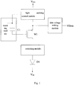
- Fig.1 shows schematically configuration of a compensation pixel circuit of a first embodiment of the present disclosure.
- the circuit comprises an organic light emitting diode D1 and a driving transistor M1.
- a first terminal of the driving transistor M1 is connected to an anode of the organic light emitting diode D1 via a switching module.
- the compensation pixel circuit further comprises:
- the first terminal of the driving transistor M1 herein refers to a terminal connected to the anode of the organic light emitting diode D1. This terminal may be a source or a drain of the transistor depending on different types of selected transistors.
- the resetting module is configured to make the gate of the driving transistor M1 discharge so that the gate voltage is reduced to magnitude of the threshold voltage of the organic light emitting diode D1, and it includes the capacitor C1 whose first terminal is connected to the gate of the driving transistor M1, this discharging process is completed apparently by the capacitor C1.
- the anode of D1 has to be connected to one terminal of the capacitor C, the gate terminal of M1, the second terminal of C1 and the anode of D1 have to be connected to one point in order to realize such function, i.e., connecting the second terminal of the capacitor C1 to a constant voltage having a higher voltage value compared with an operating voltage at a low level, so that a potential at the gate of the driving transistor M1 is discharged via D1, thereby finally making the potential at this point become the threshold voltage of D1.
- a connecting relationship of the gate of M1 being also connected to D1.
- the connecting relationship as shown in Fig.1 is also comprised in the description about the configuration or function.
- the compensation pixel circuit can be divided into three operating phases in time order, i.e., a resetting phase, a data voltage writing phase and a light emitting phase.
- the whole operating process is performed sequentially according to the order of the resetting module, the data writing module and the light emitting module. That is, the three modules realize their major functions in sequence in the three operating phases corresponding to the three modules, and the switching module and the data writing module realize their functions simultaneously.
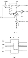
- Fig.2 schematically shows a circuit structure of a 7T1C compensation pixel circuit in an embodiment of the present disclosure.
- the circuit comprises the organic light emitting diode D1, the driving transistor M1, second to seventh switching elements M2-M7 and the storage capacitor C1.
- the resetting module further comprises a sixth switching element M6 and a seventh switching element M7.
- a first terminal and a second terminal of the sixth switching element M6 are connected to the gate and the first terminal of the driving transistor M1 respectively.
- a second terminal of the seventh switching element M7 is connected to a predetermined voltage Vinitial, and a first terminal thereof is connected to the second terminal of the capacitor C1.
- Gates of the sixth switching element M6 and the seventh switching element M7 are connected to a signal line G2.
- the signal line G2 is configured to control the two switching elements M6 and M7 to be in a turn-on state when the resetting module and the data voltage writing module are operating and to be in a turn-off state when the light emitting control module is operating.
- the data voltage writing module comprises a third switching element M3, whose first terminal is connected to the second terminal of the driving transistor M1 and second terminal is connected to a data voltage line VData.
- a gate of the third switching element M3 is connected to a signal line G1.
- the signal line G1 is configured to control the third switching element M3 to be in the turn-on state when the data voltage writing module is operating and to be in the turn-off state when the resetting module and the light emitting control module are operating.
- the light emitting control module comprises a fourth switching element M4 and a fifth switching element M5 whose second terminals are connected to an operation voltage line V DD at the high level.
- a first terminal of the fourth switching element M4 is connected to the second terminal of the driving transistor M1.
- a first terminal of the fifth switching element M5 is connected to the second terminal of the capacitor C1.
- Gates of the fourth switching element M4 and the fifth switching element M5 are connected to a signal line EMI.
- the signal line EMI is configured to control the two switching elements M4 and M5 to be in the turn-off state when the resetting module and the data voltage writing module are operating and to be in the turn-on state when the light emitting control module is operating.
- the switching module comprises a second switching element M2, whose first terminal is connected to the anode of the organic light emitting diode D1, and second terminal is connected to the first terminal of the driving transistor M1.
- the switching module is configured to disconnect the driving transistor M1 from the organic light emitting diode D1 when the data voltage VData is supplied to the second terminal of the driving transistor M1, a signal EM2 connected to the control terminal of the second switching element M2 is actually an inverse signal of the signal G1.
- the switching element refers to an element whose first terminal and second terminal are controlled by a signal of the control terminal to be connected or disconnected.
- the switching element can be implemented by a variety of specific electrical elements.
- the driving transistor M1 and the organic light emitting diode D1 constitute the basic OLED driving relationship, while the second to seventh switching elements M2-M7 can be controlled to be in the turn-on/turn-off state by the signals of their respective control terminals connected thereto.
- the second to seventh switching elements M2-M7 can be controlled to be in the turn-on/turn-off state by the signals of their respective control terminals connected thereto.
- zero points of potentials of all the bias voltages are connected to a same common terminal, and zero points of potentials of all the signal voltages are connected to a same common terminal.
- the driving transistor and the second to seventh switching elements are thin film transistors TFTs.
- the thin film transistors adopted in the present embodiment are P type channel thin film transistors.
- the first terminals of the driving transistor and the second to seventh switching elements represent drains
- the second terminals thereof represent sources
- the control terminals of the second to seventh switching element represent gates.
- other types of transistors can also be used as equivalent substitutes.
- the compensation pixel circuit comprises seven TFTs and one capacitor, it can be called as a new type 7T1C compensation pixel circuit in a naming manner conventionally used in the art.
- Fig.3 shows schematically an operation timing of the 7T1C compensation pixel circuit in the embodiment of the present disclosure. Based on the 7T1C compensating pixel circuit under the above exemplary condition, the operating principle of the circuit can be described below by referring to Fig.3 .
- the operating process of the circuit can be divided into for example three phases in general, i.e., a resetting phase (a-b), a data writing phase (b-c), and light emitting phase (c-).
- a-b resetting phase
- b-c data writing phase
- c- light emitting phase
- the signal EM1 and the signal G1 are at the high level, so that the transistors M3, M4, M5 are in the turn-off state; whereas the signals EM2 and G2 are at the low level, and the low level of the signal EM2 makes the transistor M2 turned on, and at the same time makes nodes C and D of the source and drain of the transistor M2 turned on and connected.
- the low level of the signal G2 makes the transistors M6 and M7 turned on, so that the turn-on of the transistor M7 makes the potential at a node A of the storage capacitor C1 is reset as the signal Vinitial.
- the turn-on of the transistor M6 makes the gate and drain of driving transistor M 1 connected to each other.
- the nodes B, C, and D are then connected to each other, and the potential at the node B of the storage capacitor C1 is discharged to a low voltage via the organic light emitting diode D1.
- This low voltage is the threshold voltage of the organic light emitting diode D1.
- the organic light emitting diode D1 is now in the turn-off state and does not emit light.
- the signal EM2 becomes the high level, so that the transistor M2 is turned off.
- the signal G2 is maintained at the low level, and at the same time the signal G1 also becomes the low level, so that the transistor M3 is turned on, and the data signal VData is written into the source of the driving transistor M1 via the transistor M3.
- the transistor M1 connected to OLED operates in a saturation region, and then the potential at the node B becomes VData+Vth.
- the potential at the node A is Vinitial
- the potentials at the two terminals of the storage capacitor C1 becomes Vinitial and VData+Vth respectively.
- the signals G1 and G2 become the high level, so that the transistors M3, M6 and M7 are turned off.
- the signals EM1 and EM2 become the low level, so that the transistors M4, M5 and M2 are turned on.
- the potential at the node A of the storage capacitor C1 becomes V DD from Vinitial.
- the potential at the node A becomes V DD +VData+Vth-Vinitial.
- the transistor M1 is in the saturation region.
- K in the same structure is stable relatively and can be regarded as a constant herein.
- the current flowing through the organic light emitting diode D1 connected to the drain of the driving transistor M1 is only related to Vinitial and VData, but is not unrelated to Vth and V DD .
- Vinitial does not form a current loop
- the gate voltage of the driving transistor M1 can be reset to a fixed value each time under the effect of the resetting module, and would not be affected by the IR drop (voltage drop, i.e., the voltage attenuation of the gate signal line described in the background section) phenomenon.
- the problem of the current flowing through OLED being non-uniform in magnitude is not caused by the non-uniformity of the threshold voltage Vth due to the manufacturing process of the backplane, that is, the problem of non-uniformity of light emitting is not caused.
- the potential at the node A of the storage capacitor C1 is always the signal V DD in the process of light emitting, and no charge loss occurs, which ensures the stability of the potential at the node A, so that the current flowing through the driving transistor M1 is stable, and thus the organic light emitting diode D1 emits light stably.
- the above embodiment is only used to describe the technical solution of the present disclosure, but not to limit the present disclosure.
- the present disclosure is described in detail by referring to the above embodiments, those ordinary skilled in the art shall understand that no matter what kind of structure the resetting module, the data writing module and the light emitting control module and the switching module adopt in a specific implementation process, the present disclosure can be implemented by referring to the operating principle described in the embodiment of the present disclosure only if the resetting module, the data writing module and the light emitting control module and the switching module have the function of the above compensation pixel circuit, which certainly does not depart from the scope of the technical solutions of the embodiment of the present disclosure.
- an embodiment of the present disclosure further provides a display apparatus comprising any one of the compensation pixel circuits described above.
- the display apparatus may be any product or component having the function of displaying, such as an OLED panel, a mobile phone, a tablet computer, a television, a display, a notebook computer, and a digital photo frame, and a navigator and the like.
- the circuit is designed to be a pixel unit in the array substrate, since the signal lines G1 and G2 are signals being configured to control the data voltage writing, according to the high level or the low level of the gate driving signal, one of the signals G1 and G2 can be connected to the gate line corresponding to the row while the other thereof is made to be its inverse signal.
- the signal lines EM1 and G2 they are configured to reset the gate voltage, and thus the signal lines EM1 and G2 can be implemented by designing corresponding resetting switch signal lines or can be obtained through certain logic circuit operation according to the gate line signal.
- the display apparatus provided in the embodiment of the present disclosure can solve the same technical problem and produce the same technical effect because it has the same technical features as any one of the compensation pixel circuits as described above.
- the configuration of the compensation pixel circuit made the current that finally drives OLED to emit light is unrelated to the threshold voltage Vth and the bias voltage V DD , so that the compensation pixel circuit can not only compensate for the OLED current difference due to the threshold voltage offset but also have the function of compensating for the influence of the signal voltage attenuation on the current.
- the resetting module in the circuit can reset the gate voltage of the driving transistor, i.e., making that the upper frame signal has little impact on the lower frame signal, thereby reducing influence of signals from frame to frame greatly.
- the compensation pixel circuit and the display apparatus have not only the function of compensating for the threshold voltage offset but also the function of resetting the gate voltage of the driving transistor, thereby reducing influence of signals from frame to frame greatly and at the same time ensuring the non-uniformity and stability of the light emitting of OLED.
Landscapes
- Engineering & Computer Science (AREA)
- Physics & Mathematics (AREA)
- Computer Hardware Design (AREA)
- General Physics & Mathematics (AREA)
- Theoretical Computer Science (AREA)
- Control Of El Displays (AREA)
- Electroluminescent Light Sources (AREA)
- Control Of Indicators Other Than Cathode Ray Tubes (AREA)
Claims (3)
- Appareil d'affichage comprenant une pluralité de circuits de pixel de compensation, dans lequel chacun de la pluralité de circuits de pixel de compensation comprend :une diode émettrice de lumière organique, OLED, (D1) ;un transistor de pilotage (M1) ;un module de réinitialisation qui inclut un condensateur (C1) dont une première borne est connectée à une grille du transistor de pilotage (M1) et qui est configuré de manière à ce qu'il décharge un potentiel au niveau de la grille du transistor de pilotage (M1) sous la commande d'une première ligne de signal (G2) ;un module d'écriture de tension de données qui est configuré de manière à ce qu'il alimente une tension de données (VData) sur une seconde borne du transistor de pilotage (M1) sous la commande d'une deuxième ligne de signal (G1) ;un module de commande d'émission de lumière qui est configuré de manière à ce qu'il connecte la seconde borne du transistor de pilotage (M1) à une tension de fonctionnement (VDD) à un niveau haut sous la commande d'une troisième ligne de signal (EM1) ; etun module de commutation qui est connecté entre une première borne du transistor de pilotage (M1) et une anode de l'OLED et qui est configuré de manière à ce qu'il déconnecte le transistor de pilotage (M1) vis-à-vis de l'OLED (D1) sous la commande d'une quatrième ligne de signal (EM2) ; dans lequel :
le module de commande d'émission de lumière est en outre configuré de manière à ce qu'il connecte une seconde borne du condensateur (C1) à la tension de fonctionnement (VDD) à un niveau haut sous la commande de la troisième ligne de signal (EM1) ; dans lequel :
le module d'écriture de tension de données comprend un élément de commutation d'écriture de tension de données (M3) qui comporte une borne de commande qui est connectée à la deuxième ligne de signal (G1), une première borne qui est connectée à la seconde borne du transistor de pilotage (M1) et une seconde borne qui est connectée à la tension de données (Data) ; et dans lequel :
le module de commande d'émission de lumière comprend :un premier élément de commutation de commande d'émission de lumière (M4) qui comporte une borne de commande qui est connectée à la troisième ligne de signal (EM1), une première borne qui est connectée à la seconde borne du transistor de pilotage (M1) et une seconde borne qui est connectée à la tension de fonctionnement (VDD) ; etun deuxième élément de commutation de commande d'émission de lumière (M5) qui comporte une borne de commande qui est connectée à la troisième ligne de signal (EM1), une première borne qui est connectée à la seconde borne du condensateur (C1) et une seconde borne ; dans lequel :
le module de réinitialisation comprend en outre un premier élément de commutation de réinitialisation (M6) et un deuxième élément de commutation de réinitialisation (M7) ; dans lequel :une première borne et une seconde borne du premier élément de commutation de réinitialisation (M6) sont respectivement connectées à la grille et à la première borne du transistor de pilotage (M1), et une borne de commande du premier élément de commutation de réinitialisation (M6) est connectée à la première ligne de signal (G2) ; etune seconde borne du deuxième élément de commutation de réinitialisation (M7) est connectée à une tension prédéterminée (Vinitial) et sa première borne est connectée à la seconde borne du condensateur (C1) ;caractérisé en ce que :une borne de commande du deuxième élément de commutation de réinitialisation (M7) est connectée à la première ligne de signal (G2) ;la seconde borne du deuxième élément de commutation de commande d'émission de lumière (M5) est connectée directement à la tension de fonctionnement. - Appareil d'affichage selon la revendication 1, dans lequel le module de commutation comprend un élément de commutation (M2) dont une première borne est connectée à l'anode de l'OLED (D1), dont une seconde borne est connectée à la première borne du transistor de pilotage (M1) et dont une borne de commande est connectée à la quatrième ligne de signal (EM2).
- Appareil d'affichage selon l'une quelconque des revendications 1 et 2, dans lequel le transistor de pilotage (M1) ainsi que les deuxième à septième éléments de commutation (M2-M7) sont des transistors à film mince.
Applications Claiming Priority (2)
| Application Number | Priority Date | Filing Date | Title |
|---|---|---|---|
| CN201410194265.XA CN103985352B (zh) | 2014-05-08 | 2014-05-08 | 补偿像素电路及显示装置 |
| PCT/CN2014/087897 WO2015169043A1 (fr) | 2014-05-08 | 2014-09-30 | Circuit de pixel de compensation et dispositif d'affichage |
Publications (3)
| Publication Number | Publication Date |
|---|---|
| EP3142099A1 EP3142099A1 (fr) | 2017-03-15 |
| EP3142099A4 EP3142099A4 (fr) | 2017-10-18 |
| EP3142099B1 true EP3142099B1 (fr) | 2019-07-24 |
Family
ID=51277299
Family Applications (1)
| Application Number | Title | Priority Date | Filing Date |
|---|---|---|---|
| EP14861144.5A Active EP3142099B1 (fr) | 2014-05-08 | 2014-09-30 | Circuit de pixel de compensation et dispositif d'affichage |
Country Status (4)
| Country | Link |
|---|---|
| US (1) | US9478164B2 (fr) |
| EP (1) | EP3142099B1 (fr) |
| CN (1) | CN103985352B (fr) |
| WO (1) | WO2015169043A1 (fr) |
Families Citing this family (41)
| Publication number | Priority date | Publication date | Assignee | Title |
|---|---|---|---|---|
| CN103985352B (zh) | 2014-05-08 | 2017-03-08 | 京东方科技集团股份有限公司 | 补偿像素电路及显示装置 |
| CN104464643B (zh) * | 2014-12-29 | 2017-05-03 | 上海和辉光电有限公司 | 显示装置、像素驱动电路及其驱动方法 |
| CN104680976B (zh) * | 2015-02-09 | 2017-02-22 | 京东方科技集团股份有限公司 | 像素补偿电路、显示装置及驱动方法 |
| CN104680980B (zh) | 2015-03-25 | 2017-02-15 | 京东方科技集团股份有限公司 | 像素驱动电路及其驱动方法、显示装置 |
| CN104680981B (zh) * | 2015-03-26 | 2017-03-15 | 京东方科技集团股份有限公司 | Oled像素驱动电路及驱动方法、oled显示装置 |
| TWI543143B (zh) * | 2015-04-16 | 2016-07-21 | 友達光電股份有限公司 | 像素控制電路及像素陣列控制電路 |
| CN104933991B (zh) * | 2015-07-06 | 2018-10-23 | 京东方科技集团股份有限公司 | 像素驱动电路、显示基板及其驱动方法、显示装置 |
| CN105225626B (zh) | 2015-10-13 | 2018-02-02 | 上海天马有机发光显示技术有限公司 | 有机发光二极管像素驱动电路、其显示面板及显示装置 |
| CN105427800B (zh) * | 2016-01-06 | 2018-06-12 | 京东方科技集团股份有限公司 | 像素电路、驱动方法、有机电致发光显示面板及显示装置 |
| KR102579142B1 (ko) | 2016-06-17 | 2023-09-19 | 삼성디스플레이 주식회사 | 화소와 이를 이용한 유기전계발광 표시장치 및 그의 구동방법 |
| CN106027013B (zh) * | 2016-06-23 | 2020-05-12 | 昂宝电子(上海)有限公司 | 用于模拟功率开关的控制装置和控制方法 |
| KR102559544B1 (ko) | 2016-07-01 | 2023-07-26 | 삼성디스플레이 주식회사 | 표시 장치 |
| CN106205491B (zh) * | 2016-07-11 | 2018-09-11 | 京东方科技集团股份有限公司 | 一种像素电路、其驱动方法及相关装置 |
| CN108172173A (zh) * | 2016-12-07 | 2018-06-15 | 上海和辉光电有限公司 | 一种有机发光显示器的像素电路及驱动方法 |
| CN107293257B (zh) * | 2017-07-20 | 2019-06-04 | 上海天马有机发光显示技术有限公司 | 显示面板、其显示方法及显示装置 |
| CN107342048A (zh) * | 2017-08-17 | 2017-11-10 | 京东方科技集团股份有限公司 | 像素电路及其驱动方法、显示装置 |
| CN107358918B (zh) * | 2017-08-25 | 2023-11-21 | 京东方科技集团股份有限公司 | 一种像素电路及其驱动方法、显示装置 |
| US11348524B2 (en) | 2017-09-30 | 2022-05-31 | Boe Technology Group Co., Ltd. | Display substrate and display device |
| CN109599062A (zh) * | 2017-09-30 | 2019-04-09 | 京东方科技集团股份有限公司 | 像素电路及其驱动方法、显示装置 |
| CN109872670B (zh) * | 2017-12-05 | 2021-11-05 | 京东方科技集团股份有限公司 | 显示屏、显示装置、显示电路及其亮度补偿方法 |
| CN108172172B (zh) * | 2017-12-22 | 2019-12-31 | 武汉华星光电半导体显示技术有限公司 | 像素驱动电路及具有该像素驱动电路的显示装置 |
| CN108230982A (zh) * | 2018-01-19 | 2018-06-29 | 京东方科技集团股份有限公司 | 像素驱动电路及方法、显示面板 |
| TWI662530B (zh) | 2018-06-08 | 2019-06-11 | 友達光電股份有限公司 | 發光二極體裝置及其控制方法 |
| CN108922474B (zh) * | 2018-06-22 | 2020-06-09 | 武汉华星光电半导体显示技术有限公司 | 一种像素补偿电路及其驱动方法、amoled显示面板 |
| CN108538249B (zh) * | 2018-06-22 | 2021-05-07 | 京东方科技集团股份有限公司 | 像素驱动电路及方法、显示装置 |
| CN109192140B (zh) * | 2018-09-27 | 2020-11-24 | 武汉华星光电半导体显示技术有限公司 | 像素驱动电路和显示装置 |
| CN109509428B (zh) * | 2019-01-07 | 2021-01-08 | 京东方科技集团股份有限公司 | 像素驱动电路、像素驱动方法和显示装置 |
| CN109637424A (zh) * | 2019-01-24 | 2019-04-16 | 深圳市华星光电半导体显示技术有限公司 | Goa电路及显示面板 |
| CN109887466B (zh) * | 2019-04-19 | 2021-03-30 | 京东方科技集团股份有限公司 | 像素驱动电路及方法、显示面板 |
| JP7529758B2 (ja) | 2020-03-19 | 2024-08-06 | 京東方科技集團股▲ふん▼有限公司 | 表示基板及び表示装置 |
| US12317703B2 (en) | 2020-03-19 | 2025-05-27 | Boe Technology Group Co., Ltd. | Display substrate having connection electrode in a same layer with one capacitor electrode and electrically connecting the other capacitor electrode to data writing sub-circuit, and display device |
| EP4123711A4 (fr) | 2020-03-19 | 2023-05-03 | BOE Technology Group Co., Ltd. | Substrat d'affichage et appareil d'affichage |
| CN111508437A (zh) * | 2020-04-29 | 2020-08-07 | 武汉华星光电半导体显示技术有限公司 | 一种像素驱动电路及其驱动方法、显示面板及显示装置 |
| CN111583864B (zh) * | 2020-06-11 | 2021-09-03 | 京东方科技集团股份有限公司 | 显示驱动电路及其驱动方法、显示装置 |
| CN111564141A (zh) * | 2020-06-15 | 2020-08-21 | 京东方科技集团股份有限公司 | 补偿电路及其补偿方法、像素电路以及显示装置 |
| KR102819178B1 (ko) | 2020-10-21 | 2025-06-10 | 엘지디스플레이 주식회사 | 유기 발광 표시 장치 |
| CN115104148B8 (zh) * | 2020-11-30 | 2026-02-06 | 京东方科技集团股份有限公司 | 像素电路、驱动方法、显示基板和显示装置 |
| CN112885291A (zh) * | 2021-01-15 | 2021-06-01 | 合肥维信诺科技有限公司 | 像素电路及其驱动方法、显示面板 |
| JP2023050791A (ja) * | 2021-09-30 | 2023-04-11 | セイコーエプソン株式会社 | 電気光学装置、電子機器および電気光学装置の駆動方法 |
| US12283239B2 (en) | 2022-01-13 | 2025-04-22 | Chengdu Boe Optoelectronics Technology Co., Ltd. | Driving circuit, driving method and display device |
| CN117153103A (zh) * | 2023-08-24 | 2023-12-01 | 北京欧铼德微电子技术有限公司 | 像素电路及驱动方法、显示面板 |
Citations (1)
| Publication number | Priority date | Publication date | Assignee | Title |
|---|---|---|---|---|
| US20140078233A1 (en) * | 2012-09-20 | 2014-03-20 | Canon Kabushiki Kaisha | Light emitting apparatus, driving circuit of light emitting element, and driving method |
Family Cites Families (13)
| Publication number | Priority date | Publication date | Assignee | Title |
|---|---|---|---|---|
| KR100952827B1 (ko) * | 2007-12-04 | 2010-04-15 | 삼성모바일디스플레이주식회사 | 화소 및 그를 이용한 유기전계발광표시장치 |
| KR100911980B1 (ko) * | 2008-03-28 | 2009-08-13 | 삼성모바일디스플레이주식회사 | 화소 및 이를 이용한 유기전계발광 표시장치 |
| KR101525807B1 (ko) * | 2009-02-05 | 2015-06-05 | 삼성디스플레이 주식회사 | 표시 장치및 그 구동 방법 |
| CN102693696B (zh) * | 2011-04-08 | 2016-08-03 | 京东方科技集团股份有限公司 | 像素电路结构及驱动像素电路结构的方法 |
| TW201316315A (zh) * | 2011-10-05 | 2013-04-16 | Wintek Corp | 發光元件驅動電路及其相關的畫素電路與應用 |
| CN103050080B (zh) * | 2011-10-11 | 2015-08-12 | 上海天马微电子有限公司 | 有机发光显示器的像素电路及其驱动方法 |
| CN202394497U (zh) * | 2011-11-15 | 2012-08-22 | 四川虹视显示技术有限公司 | 一种像素驱动电路 |
| CN102881253B (zh) * | 2012-09-21 | 2015-09-09 | 京东方科技集团股份有限公司 | 一种像素电路和薄膜晶体管背板 |
| CN103150991A (zh) | 2013-03-14 | 2013-06-12 | 友达光电股份有限公司 | 一种用于amoled显示器的像素补偿电路 |
| CN103236238B (zh) * | 2013-04-26 | 2015-07-22 | 北京京东方光电科技有限公司 | 像素单元控制电路以及显示装置 |
| CN203250518U (zh) * | 2013-05-31 | 2013-10-23 | 京东方科技集团股份有限公司 | 像素电路、有机发光显示面板及显示装置 |
| CN203812537U (zh) * | 2014-05-08 | 2014-09-03 | 京东方科技集团股份有限公司 | 补偿像素电路及显示装置 |
| CN103985352B (zh) | 2014-05-08 | 2017-03-08 | 京东方科技集团股份有限公司 | 补偿像素电路及显示装置 |
-
2014
- 2014-05-08 CN CN201410194265.XA patent/CN103985352B/zh active Active
- 2014-09-30 US US14/443,511 patent/US9478164B2/en active Active
- 2014-09-30 EP EP14861144.5A patent/EP3142099B1/fr active Active
- 2014-09-30 WO PCT/CN2014/087897 patent/WO2015169043A1/fr not_active Ceased
Patent Citations (1)
| Publication number | Priority date | Publication date | Assignee | Title |
|---|---|---|---|---|
| US20140078233A1 (en) * | 2012-09-20 | 2014-03-20 | Canon Kabushiki Kaisha | Light emitting apparatus, driving circuit of light emitting element, and driving method |
Also Published As
| Publication number | Publication date |
|---|---|
| CN103985352A (zh) | 2014-08-13 |
| US20150348462A1 (en) | 2015-12-03 |
| US9478164B2 (en) | 2016-10-25 |
| EP3142099A4 (fr) | 2017-10-18 |
| WO2015169043A1 (fr) | 2015-11-12 |
| CN103985352B (zh) | 2017-03-08 |
| EP3142099A1 (fr) | 2017-03-15 |
Similar Documents
| Publication | Publication Date | Title |
|---|---|---|
| EP3142099B1 (fr) | Circuit de pixel de compensation et dispositif d'affichage | |
| US10902781B2 (en) | Pixel circuit, driving method, organic light emitting display panel, and display device | |
| US9875691B2 (en) | Pixel circuit, driving method thereof and display device | |
| US9564081B2 (en) | Pixel compensation circuit, array substrate and display apparatus | |
| US9734763B2 (en) | Pixel circuit, driving method and display apparatus | |
| CN104575398B (zh) | 像素电路及其驱动方法、显示装置 | |
| US9262966B2 (en) | Pixel circuit, display panel and display apparatus | |
| US11450270B2 (en) | Pixel circuit and method of driving the same, display device | |
| US20180286313A1 (en) | Pixel circuit, driving method thereof, array substrate, display device | |
| US9437142B2 (en) | Pixel circuit and display apparatus | |
| CN105161051A (zh) | 像素电路及其驱动方法、阵列基板、显示面板及显示装置 | |
| WO2017045357A1 (fr) | Circuit de pixel et procédé de pilotage, panneau d'affichage et dispositif d'affichage associés | |
| CN104751804A (zh) | 一种像素电路、其驱动方法及相关装置 | |
| CN106971691A (zh) | 一种像素电路、驱动方法及显示装置 | |
| US20160300531A1 (en) | Pixel circuit and display apparatus | |
| WO2015196730A1 (fr) | Circuit de pixels, son procédé d'attaque et appareil d'affichage | |
| EP3660825A1 (fr) | Circuit de pixels et procédé de commande associé, panneau d'affichage et appareil d'affichage | |
| US20180247592A1 (en) | Pixel Driving Circuit and Driving Method Thereof, Array Substrate, and Display Device | |
| CN106297663B (zh) | 一种像素电路、其驱动方法及相关装置 | |
| US11170714B2 (en) | Pixel circuit, method for driving the same, display panel and display device | |
| US20160247447A1 (en) | Pixel circuit and display apparatus | |
| CN104078003B (zh) | 像素电路和显示装置 | |
| JP6196809B2 (ja) | 画素回路及びその駆動方法 | |
| CN104700781B (zh) | 像素电路及其驱动方法、显示装置 | |
| CN203950535U (zh) | 像素电路和显示装置 |
Legal Events
| Date | Code | Title | Description |
|---|---|---|---|
| PUAI | Public reference made under article 153(3) epc to a published international application that has entered the european phase |
Free format text: ORIGINAL CODE: 0009012 |
|
| STAA | Information on the status of an ep patent application or granted ep patent |
Free format text: STATUS: REQUEST FOR EXAMINATION WAS MADE |
|
| 17P | Request for examination filed |
Effective date: 20150519 |
|
| AK | Designated contracting states |
Kind code of ref document: A1 Designated state(s): AL AT BE BG CH CY CZ DE DK EE ES FI FR GB GR HR HU IE IS IT LI LT LU LV MC MK MT NL NO PL PT RO RS SE SI SK SM TR |
|
| AX | Request for extension of the european patent |
Extension state: BA ME |
|
| DAX | Request for extension of the european patent (deleted) | ||
| REG | Reference to a national code |
Ref country code: DE Ref legal event code: R079 Ref document number: 602014050632 Country of ref document: DE Free format text: PREVIOUS MAIN CLASS: G09G0003320000 Ipc: G09G0003323300 |
|
| A4 | Supplementary search report drawn up and despatched |
Effective date: 20170914 |
|
| RIC1 | Information provided on ipc code assigned before grant |
Ipc: G09G 3/3233 20160101AFI20170908BHEP |
|
| STAA | Information on the status of an ep patent application or granted ep patent |
Free format text: STATUS: EXAMINATION IS IN PROGRESS |
|
| 17Q | First examination report despatched |
Effective date: 20180706 |
|
| GRAP | Despatch of communication of intention to grant a patent |
Free format text: ORIGINAL CODE: EPIDOSNIGR1 |
|
| STAA | Information on the status of an ep patent application or granted ep patent |
Free format text: STATUS: GRANT OF PATENT IS INTENDED |
|
| INTG | Intention to grant announced |
Effective date: 20190215 |
|
| GRAS | Grant fee paid |
Free format text: ORIGINAL CODE: EPIDOSNIGR3 |
|
| GRAA | (expected) grant |
Free format text: ORIGINAL CODE: 0009210 |
|
| STAA | Information on the status of an ep patent application or granted ep patent |
Free format text: STATUS: THE PATENT HAS BEEN GRANTED |
|
| AK | Designated contracting states |
Kind code of ref document: B1 Designated state(s): AL AT BE BG CH CY CZ DE DK EE ES FI FR GB GR HR HU IE IS IT LI LT LU LV MC MK MT NL NO PL PT RO RS SE SI SK SM TR |
|
| REG | Reference to a national code |
Ref country code: GB Ref legal event code: FG4D |
|
| REG | Reference to a national code |
Ref country code: CH Ref legal event code: EP |
|
| REG | Reference to a national code |
Ref country code: DE Ref legal event code: R096 Ref document number: 602014050632 Country of ref document: DE |
|
| REG | Reference to a national code |
Ref country code: AT Ref legal event code: REF Ref document number: 1159149 Country of ref document: AT Kind code of ref document: T Effective date: 20190815 |
|
| REG | Reference to a national code |
Ref country code: IE Ref legal event code: FG4D |
|
| REG | Reference to a national code |
Ref country code: NL Ref legal event code: FP |
|
| REG | Reference to a national code |
Ref country code: LT Ref legal event code: MG4D |
|
| REG | Reference to a national code |
Ref country code: AT Ref legal event code: MK05 Ref document number: 1159149 Country of ref document: AT Kind code of ref document: T Effective date: 20190724 |
|
| PG25 | Lapsed in a contracting state [announced via postgrant information from national office to epo] |
Ref country code: PT Free format text: LAPSE BECAUSE OF FAILURE TO SUBMIT A TRANSLATION OF THE DESCRIPTION OR TO PAY THE FEE WITHIN THE PRESCRIBED TIME-LIMIT Effective date: 20191125 Ref country code: FI Free format text: LAPSE BECAUSE OF FAILURE TO SUBMIT A TRANSLATION OF THE DESCRIPTION OR TO PAY THE FEE WITHIN THE PRESCRIBED TIME-LIMIT Effective date: 20190724 Ref country code: LT Free format text: LAPSE BECAUSE OF FAILURE TO SUBMIT A TRANSLATION OF THE DESCRIPTION OR TO PAY THE FEE WITHIN THE PRESCRIBED TIME-LIMIT Effective date: 20190724 Ref country code: SE Free format text: LAPSE BECAUSE OF FAILURE TO SUBMIT A TRANSLATION OF THE DESCRIPTION OR TO PAY THE FEE WITHIN THE PRESCRIBED TIME-LIMIT Effective date: 20190724 Ref country code: HR Free format text: LAPSE BECAUSE OF FAILURE TO SUBMIT A TRANSLATION OF THE DESCRIPTION OR TO PAY THE FEE WITHIN THE PRESCRIBED TIME-LIMIT Effective date: 20190724 Ref country code: BG Free format text: LAPSE BECAUSE OF FAILURE TO SUBMIT A TRANSLATION OF THE DESCRIPTION OR TO PAY THE FEE WITHIN THE PRESCRIBED TIME-LIMIT Effective date: 20191024 Ref country code: AT Free format text: LAPSE BECAUSE OF FAILURE TO SUBMIT A TRANSLATION OF THE DESCRIPTION OR TO PAY THE FEE WITHIN THE PRESCRIBED TIME-LIMIT Effective date: 20190724 Ref country code: NO Free format text: LAPSE BECAUSE OF FAILURE TO SUBMIT A TRANSLATION OF THE DESCRIPTION OR TO PAY THE FEE WITHIN THE PRESCRIBED TIME-LIMIT Effective date: 20191024 |
|
| PG25 | Lapsed in a contracting state [announced via postgrant information from national office to epo] |
Ref country code: LV Free format text: LAPSE BECAUSE OF FAILURE TO SUBMIT A TRANSLATION OF THE DESCRIPTION OR TO PAY THE FEE WITHIN THE PRESCRIBED TIME-LIMIT Effective date: 20190724 Ref country code: ES Free format text: LAPSE BECAUSE OF FAILURE TO SUBMIT A TRANSLATION OF THE DESCRIPTION OR TO PAY THE FEE WITHIN THE PRESCRIBED TIME-LIMIT Effective date: 20190724 Ref country code: AL Free format text: LAPSE BECAUSE OF FAILURE TO SUBMIT A TRANSLATION OF THE DESCRIPTION OR TO PAY THE FEE WITHIN THE PRESCRIBED TIME-LIMIT Effective date: 20190724 Ref country code: GR Free format text: LAPSE BECAUSE OF FAILURE TO SUBMIT A TRANSLATION OF THE DESCRIPTION OR TO PAY THE FEE WITHIN THE PRESCRIBED TIME-LIMIT Effective date: 20191025 Ref country code: IS Free format text: LAPSE BECAUSE OF FAILURE TO SUBMIT A TRANSLATION OF THE DESCRIPTION OR TO PAY THE FEE WITHIN THE PRESCRIBED TIME-LIMIT Effective date: 20191124 Ref country code: RS Free format text: LAPSE BECAUSE OF FAILURE TO SUBMIT A TRANSLATION OF THE DESCRIPTION OR TO PAY THE FEE WITHIN THE PRESCRIBED TIME-LIMIT Effective date: 20190724 |
|
| PG25 | Lapsed in a contracting state [announced via postgrant information from national office to epo] |
Ref country code: TR Free format text: LAPSE BECAUSE OF FAILURE TO SUBMIT A TRANSLATION OF THE DESCRIPTION OR TO PAY THE FEE WITHIN THE PRESCRIBED TIME-LIMIT Effective date: 20190724 |
|
| PG25 | Lapsed in a contracting state [announced via postgrant information from national office to epo] |
Ref country code: DK Free format text: LAPSE BECAUSE OF FAILURE TO SUBMIT A TRANSLATION OF THE DESCRIPTION OR TO PAY THE FEE WITHIN THE PRESCRIBED TIME-LIMIT Effective date: 20190724 Ref country code: EE Free format text: LAPSE BECAUSE OF FAILURE TO SUBMIT A TRANSLATION OF THE DESCRIPTION OR TO PAY THE FEE WITHIN THE PRESCRIBED TIME-LIMIT Effective date: 20190724 Ref country code: PL Free format text: LAPSE BECAUSE OF FAILURE TO SUBMIT A TRANSLATION OF THE DESCRIPTION OR TO PAY THE FEE WITHIN THE PRESCRIBED TIME-LIMIT Effective date: 20190724 Ref country code: RO Free format text: LAPSE BECAUSE OF FAILURE TO SUBMIT A TRANSLATION OF THE DESCRIPTION OR TO PAY THE FEE WITHIN THE PRESCRIBED TIME-LIMIT Effective date: 20190724 Ref country code: IT Free format text: LAPSE BECAUSE OF FAILURE TO SUBMIT A TRANSLATION OF THE DESCRIPTION OR TO PAY THE FEE WITHIN THE PRESCRIBED TIME-LIMIT Effective date: 20190724 |
|
| PG25 | Lapsed in a contracting state [announced via postgrant information from national office to epo] |
Ref country code: SM Free format text: LAPSE BECAUSE OF FAILURE TO SUBMIT A TRANSLATION OF THE DESCRIPTION OR TO PAY THE FEE WITHIN THE PRESCRIBED TIME-LIMIT Effective date: 20190724 Ref country code: IS Free format text: LAPSE BECAUSE OF FAILURE TO SUBMIT A TRANSLATION OF THE DESCRIPTION OR TO PAY THE FEE WITHIN THE PRESCRIBED TIME-LIMIT Effective date: 20200224 Ref country code: SK Free format text: LAPSE BECAUSE OF FAILURE TO SUBMIT A TRANSLATION OF THE DESCRIPTION OR TO PAY THE FEE WITHIN THE PRESCRIBED TIME-LIMIT Effective date: 20190724 Ref country code: MC Free format text: LAPSE BECAUSE OF FAILURE TO SUBMIT A TRANSLATION OF THE DESCRIPTION OR TO PAY THE FEE WITHIN THE PRESCRIBED TIME-LIMIT Effective date: 20190724 Ref country code: CZ Free format text: LAPSE BECAUSE OF FAILURE TO SUBMIT A TRANSLATION OF THE DESCRIPTION OR TO PAY THE FEE WITHIN THE PRESCRIBED TIME-LIMIT Effective date: 20190724 |
|
| REG | Reference to a national code |
Ref country code: CH Ref legal event code: PL |
|
| REG | Reference to a national code |
Ref country code: DE Ref legal event code: R097 Ref document number: 602014050632 Country of ref document: DE |
|
| PLBE | No opposition filed within time limit |
Free format text: ORIGINAL CODE: 0009261 |
|
| STAA | Information on the status of an ep patent application or granted ep patent |
Free format text: STATUS: NO OPPOSITION FILED WITHIN TIME LIMIT |
|
| PG2D | Information on lapse in contracting state deleted |
Ref country code: IS |
|
| PG25 | Lapsed in a contracting state [announced via postgrant information from national office to epo] |
Ref country code: LI Free format text: LAPSE BECAUSE OF NON-PAYMENT OF DUE FEES Effective date: 20190930 Ref country code: CH Free format text: LAPSE BECAUSE OF NON-PAYMENT OF DUE FEES Effective date: 20190930 Ref country code: IE Free format text: LAPSE BECAUSE OF NON-PAYMENT OF DUE FEES Effective date: 20190930 Ref country code: LU Free format text: LAPSE BECAUSE OF NON-PAYMENT OF DUE FEES Effective date: 20190930 |
|
| 26N | No opposition filed |
Effective date: 20200603 |
|
| REG | Reference to a national code |
Ref country code: BE Ref legal event code: MM Effective date: 20190930 |
|
| PG25 | Lapsed in a contracting state [announced via postgrant information from national office to epo] |
Ref country code: BE Free format text: LAPSE BECAUSE OF NON-PAYMENT OF DUE FEES Effective date: 20190930 Ref country code: SI Free format text: LAPSE BECAUSE OF FAILURE TO SUBMIT A TRANSLATION OF THE DESCRIPTION OR TO PAY THE FEE WITHIN THE PRESCRIBED TIME-LIMIT Effective date: 20190724 |
|
| PG25 | Lapsed in a contracting state [announced via postgrant information from national office to epo] |
Ref country code: CY Free format text: LAPSE BECAUSE OF FAILURE TO SUBMIT A TRANSLATION OF THE DESCRIPTION OR TO PAY THE FEE WITHIN THE PRESCRIBED TIME-LIMIT Effective date: 20190724 |
|
| PG25 | Lapsed in a contracting state [announced via postgrant information from national office to epo] |
Ref country code: HU Free format text: LAPSE BECAUSE OF FAILURE TO SUBMIT A TRANSLATION OF THE DESCRIPTION OR TO PAY THE FEE WITHIN THE PRESCRIBED TIME-LIMIT; INVALID AB INITIO Effective date: 20140930 Ref country code: MT Free format text: LAPSE BECAUSE OF FAILURE TO SUBMIT A TRANSLATION OF THE DESCRIPTION OR TO PAY THE FEE WITHIN THE PRESCRIBED TIME-LIMIT Effective date: 20190724 |
|
| PG25 | Lapsed in a contracting state [announced via postgrant information from national office to epo] |
Ref country code: MK Free format text: LAPSE BECAUSE OF FAILURE TO SUBMIT A TRANSLATION OF THE DESCRIPTION OR TO PAY THE FEE WITHIN THE PRESCRIBED TIME-LIMIT Effective date: 20190724 |
|
| PGFP | Annual fee paid to national office [announced via postgrant information from national office to epo] |
Ref country code: DE Payment date: 20250925 Year of fee payment: 12 |
|
| PGFP | Annual fee paid to national office [announced via postgrant information from national office to epo] |
Ref country code: NL Payment date: 20250923 Year of fee payment: 12 |
|
| PGFP | Annual fee paid to national office [announced via postgrant information from national office to epo] |
Ref country code: GB Payment date: 20250922 Year of fee payment: 12 |
|
| PGFP | Annual fee paid to national office [announced via postgrant information from national office to epo] |
Ref country code: FR Payment date: 20250923 Year of fee payment: 12 |