EP3142100A1 - Pixelansteuerungsschaltung und ansteuerungsverfahren dafür sowie anzeigevorrichtung - Google Patents
Pixelansteuerungsschaltung und ansteuerungsverfahren dafür sowie anzeigevorrichtung Download PDFInfo
- Publication number
- EP3142100A1 EP3142100A1 EP14861171.8A EP14861171A EP3142100A1 EP 3142100 A1 EP3142100 A1 EP 3142100A1 EP 14861171 A EP14861171 A EP 14861171A EP 3142100 A1 EP3142100 A1 EP 3142100A1
- Authority
- EP
- European Patent Office
- Prior art keywords
- port
- signal
- driving
- switching unit
- switching
- Prior art date
- Legal status (The legal status is an assumption and is not a legal conclusion. Google has not performed a legal analysis and makes no representation as to the accuracy of the status listed.)
- Granted
Links
Images


Classifications
-
- G—PHYSICS
- G09—EDUCATION; CRYPTOGRAPHY; DISPLAY; ADVERTISING; SEALS
- G09G—ARRANGEMENTS OR CIRCUITS FOR CONTROL OF INDICATING DEVICES USING STATIC MEANS TO PRESENT VARIABLE INFORMATION
- G09G3/00—Control arrangements or circuits, of interest only in connection with visual indicators other than cathode-ray tubes
- G09G3/20—Control arrangements or circuits, of interest only in connection with visual indicators other than cathode-ray tubes for presentation of an assembly of a number of characters, e.g. a page, by composing the assembly by combination of individual elements arranged in a matrix no fixed position being assigned to or needed to be assigned to the individual characters or partial characters
- G09G3/22—Control arrangements or circuits, of interest only in connection with visual indicators other than cathode-ray tubes for presentation of an assembly of a number of characters, e.g. a page, by composing the assembly by combination of individual elements arranged in a matrix no fixed position being assigned to or needed to be assigned to the individual characters or partial characters using controlled light sources
- G09G3/30—Control arrangements or circuits, of interest only in connection with visual indicators other than cathode-ray tubes for presentation of an assembly of a number of characters, e.g. a page, by composing the assembly by combination of individual elements arranged in a matrix no fixed position being assigned to or needed to be assigned to the individual characters or partial characters using controlled light sources using electroluminescent panels
- G09G3/32—Control arrangements or circuits, of interest only in connection with visual indicators other than cathode-ray tubes for presentation of an assembly of a number of characters, e.g. a page, by composing the assembly by combination of individual elements arranged in a matrix no fixed position being assigned to or needed to be assigned to the individual characters or partial characters using controlled light sources using electroluminescent panels semiconductive, e.g. using light-emitting diodes [LED]
- G09G3/3208—Control arrangements or circuits, of interest only in connection with visual indicators other than cathode-ray tubes for presentation of an assembly of a number of characters, e.g. a page, by composing the assembly by combination of individual elements arranged in a matrix no fixed position being assigned to or needed to be assigned to the individual characters or partial characters using controlled light sources using electroluminescent panels semiconductive, e.g. using light-emitting diodes [LED] organic, e.g. using organic light-emitting diodes [OLED]
- G09G3/3225—Control arrangements or circuits, of interest only in connection with visual indicators other than cathode-ray tubes for presentation of an assembly of a number of characters, e.g. a page, by composing the assembly by combination of individual elements arranged in a matrix no fixed position being assigned to or needed to be assigned to the individual characters or partial characters using controlled light sources using electroluminescent panels semiconductive, e.g. using light-emitting diodes [LED] organic, e.g. using organic light-emitting diodes [OLED] using an active matrix
- G09G3/3233—Control arrangements or circuits, of interest only in connection with visual indicators other than cathode-ray tubes for presentation of an assembly of a number of characters, e.g. a page, by composing the assembly by combination of individual elements arranged in a matrix no fixed position being assigned to or needed to be assigned to the individual characters or partial characters using controlled light sources using electroluminescent panels semiconductive, e.g. using light-emitting diodes [LED] organic, e.g. using organic light-emitting diodes [OLED] using an active matrix with pixel circuitry controlling the current through the light-emitting element
-
- G—PHYSICS
- G09—EDUCATION; CRYPTOGRAPHY; DISPLAY; ADVERTISING; SEALS
- G09G—ARRANGEMENTS OR CIRCUITS FOR CONTROL OF INDICATING DEVICES USING STATIC MEANS TO PRESENT VARIABLE INFORMATION
- G09G3/00—Control arrangements or circuits, of interest only in connection with visual indicators other than cathode-ray tubes
- G09G3/20—Control arrangements or circuits, of interest only in connection with visual indicators other than cathode-ray tubes for presentation of an assembly of a number of characters, e.g. a page, by composing the assembly by combination of individual elements arranged in a matrix no fixed position being assigned to or needed to be assigned to the individual characters or partial characters
- G09G3/22—Control arrangements or circuits, of interest only in connection with visual indicators other than cathode-ray tubes for presentation of an assembly of a number of characters, e.g. a page, by composing the assembly by combination of individual elements arranged in a matrix no fixed position being assigned to or needed to be assigned to the individual characters or partial characters using controlled light sources
- G09G3/30—Control arrangements or circuits, of interest only in connection with visual indicators other than cathode-ray tubes for presentation of an assembly of a number of characters, e.g. a page, by composing the assembly by combination of individual elements arranged in a matrix no fixed position being assigned to or needed to be assigned to the individual characters or partial characters using controlled light sources using electroluminescent panels
- G09G3/32—Control arrangements or circuits, of interest only in connection with visual indicators other than cathode-ray tubes for presentation of an assembly of a number of characters, e.g. a page, by composing the assembly by combination of individual elements arranged in a matrix no fixed position being assigned to or needed to be assigned to the individual characters or partial characters using controlled light sources using electroluminescent panels semiconductive, e.g. using light-emitting diodes [LED]
-
- G—PHYSICS
- G09—EDUCATION; CRYPTOGRAPHY; DISPLAY; ADVERTISING; SEALS
- G09G—ARRANGEMENTS OR CIRCUITS FOR CONTROL OF INDICATING DEVICES USING STATIC MEANS TO PRESENT VARIABLE INFORMATION
- G09G3/00—Control arrangements or circuits, of interest only in connection with visual indicators other than cathode-ray tubes
- G09G3/20—Control arrangements or circuits, of interest only in connection with visual indicators other than cathode-ray tubes for presentation of an assembly of a number of characters, e.g. a page, by composing the assembly by combination of individual elements arranged in a matrix no fixed position being assigned to or needed to be assigned to the individual characters or partial characters
- G09G3/22—Control arrangements or circuits, of interest only in connection with visual indicators other than cathode-ray tubes for presentation of an assembly of a number of characters, e.g. a page, by composing the assembly by combination of individual elements arranged in a matrix no fixed position being assigned to or needed to be assigned to the individual characters or partial characters using controlled light sources
- G09G3/30—Control arrangements or circuits, of interest only in connection with visual indicators other than cathode-ray tubes for presentation of an assembly of a number of characters, e.g. a page, by composing the assembly by combination of individual elements arranged in a matrix no fixed position being assigned to or needed to be assigned to the individual characters or partial characters using controlled light sources using electroluminescent panels
- G09G3/32—Control arrangements or circuits, of interest only in connection with visual indicators other than cathode-ray tubes for presentation of an assembly of a number of characters, e.g. a page, by composing the assembly by combination of individual elements arranged in a matrix no fixed position being assigned to or needed to be assigned to the individual characters or partial characters using controlled light sources using electroluminescent panels semiconductive, e.g. using light-emitting diodes [LED]
- G09G3/3208—Control arrangements or circuits, of interest only in connection with visual indicators other than cathode-ray tubes for presentation of an assembly of a number of characters, e.g. a page, by composing the assembly by combination of individual elements arranged in a matrix no fixed position being assigned to or needed to be assigned to the individual characters or partial characters using controlled light sources using electroluminescent panels semiconductive, e.g. using light-emitting diodes [LED] organic, e.g. using organic light-emitting diodes [OLED]
- G09G3/3275—Details of drivers for data electrodes
- G09G3/3291—Details of drivers for data electrodes in which the data driver supplies a variable data voltage for setting the current through, or the voltage across, the light-emitting elements
-
- G—PHYSICS
- G09—EDUCATION; CRYPTOGRAPHY; DISPLAY; ADVERTISING; SEALS
- G09G—ARRANGEMENTS OR CIRCUITS FOR CONTROL OF INDICATING DEVICES USING STATIC MEANS TO PRESENT VARIABLE INFORMATION
- G09G2300/00—Aspects of the constitution of display devices
- G09G2300/04—Structural and physical details of display devices
- G09G2300/0421—Structural details of the set of electrodes
- G09G2300/043—Compensation electrodes or other additional electrodes in matrix displays related to distortions or compensation signals, e.g. for modifying TFT threshold voltage in column driver
-
- G—PHYSICS
- G09—EDUCATION; CRYPTOGRAPHY; DISPLAY; ADVERTISING; SEALS
- G09G—ARRANGEMENTS OR CIRCUITS FOR CONTROL OF INDICATING DEVICES USING STATIC MEANS TO PRESENT VARIABLE INFORMATION
- G09G2300/00—Aspects of the constitution of display devices
- G09G2300/08—Active matrix structure, i.e. with use of active elements, inclusive of non-linear two terminal elements, in the pixels together with light emitting or modulating elements
- G09G2300/0809—Several active elements per pixel in active matrix panels
-
- G—PHYSICS
- G09—EDUCATION; CRYPTOGRAPHY; DISPLAY; ADVERTISING; SEALS
- G09G—ARRANGEMENTS OR CIRCUITS FOR CONTROL OF INDICATING DEVICES USING STATIC MEANS TO PRESENT VARIABLE INFORMATION
- G09G2300/00—Aspects of the constitution of display devices
- G09G2300/08—Active matrix structure, i.e. with use of active elements, inclusive of non-linear two terminal elements, in the pixels together with light emitting or modulating elements
- G09G2300/0809—Several active elements per pixel in active matrix panels
- G09G2300/0819—Several active elements per pixel in active matrix panels used for counteracting undesired variations, e.g. feedback or autozeroing
-
- G—PHYSICS
- G09—EDUCATION; CRYPTOGRAPHY; DISPLAY; ADVERTISING; SEALS
- G09G—ARRANGEMENTS OR CIRCUITS FOR CONTROL OF INDICATING DEVICES USING STATIC MEANS TO PRESENT VARIABLE INFORMATION
- G09G2300/00—Aspects of the constitution of display devices
- G09G2300/08—Active matrix structure, i.e. with use of active elements, inclusive of non-linear two terminal elements, in the pixels together with light emitting or modulating elements
- G09G2300/0809—Several active elements per pixel in active matrix panels
- G09G2300/0842—Several active elements per pixel in active matrix panels forming a memory circuit, e.g. a dynamic memory with one capacitor
- G09G2300/0861—Several active elements per pixel in active matrix panels forming a memory circuit, e.g. a dynamic memory with one capacitor with additional control of the display period without amending the charge stored in a pixel memory, e.g. by means of additional select electrodes
-
- G—PHYSICS
- G09—EDUCATION; CRYPTOGRAPHY; DISPLAY; ADVERTISING; SEALS
- G09G—ARRANGEMENTS OR CIRCUITS FOR CONTROL OF INDICATING DEVICES USING STATIC MEANS TO PRESENT VARIABLE INFORMATION
- G09G2310/00—Command of the display device
- G09G2310/02—Addressing, scanning or driving the display screen or processing steps related thereto
- G09G2310/0243—Details of the generation of driving signals
- G09G2310/0251—Precharge or discharge of pixel before applying new pixel voltage
-
- G—PHYSICS
- G09—EDUCATION; CRYPTOGRAPHY; DISPLAY; ADVERTISING; SEALS
- G09G—ARRANGEMENTS OR CIRCUITS FOR CONTROL OF INDICATING DEVICES USING STATIC MEANS TO PRESENT VARIABLE INFORMATION
- G09G2310/00—Command of the display device
- G09G2310/02—Addressing, scanning or driving the display screen or processing steps related thereto
- G09G2310/0262—The addressing of the pixel, in a display other than an active matrix LCD, involving the control of two or more scan electrodes or two or more data electrodes, e.g. pixel voltage dependent on signals of two data electrodes
-
- G—PHYSICS
- G09—EDUCATION; CRYPTOGRAPHY; DISPLAY; ADVERTISING; SEALS
- G09G—ARRANGEMENTS OR CIRCUITS FOR CONTROL OF INDICATING DEVICES USING STATIC MEANS TO PRESENT VARIABLE INFORMATION
- G09G2320/00—Control of display operating conditions
- G09G2320/04—Maintaining the quality of display appearance
- G09G2320/043—Preventing or counteracting the effects of ageing
Definitions
- the present invention relates to the technical field of display, in particular to a pixel driving circuit, a driving method for the pixel driving circuit and a display device.
- AMOLED Active matrix organic light emitting diode
- OLED Organic light emitting diode
- PDA Personal Digital Assistant, or palmtop computer
- digital camera OLED has begun to replace the traditional LCD display screen.
- the pixel driving circuit design is the core technical content of AMOLED display, which has important research significance.
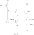
- the driving current I OLED is a current generated by applying the voltage Vdata , provided by the data line on the saturation region of the driving transistor (DTFT).
- This current drives the OLED for emitting light
- the V GS is the voltage between the gate and the source of the driving transistor
- the Vth is the threshold voltage of the driving transistor.
- the threshold voltages ( Vth ) of the driving TFTs of individual pixels are uneven. Since the threshold voltages of the driving TFTs (i.e., T2 in Fig. 1 ) of individual pixels are uneven, there is difference between the currents flowing through the OLEDs of individual pixels, affecting the display effect of the entire image.
- the pixel driving circuit the driving method for the pixel driving circuit and the display device, the situation that driving currents of an active light emitting device are affected by threshold voltage shift of a driving transistor can be avoided, and therefore the evenness of a displayed image is improved.
- a pixel driving circuit comprises a light emitting device, a storage capacitor, a driving unit and five switching units; wherein each switching unit comprises a control port, a first signal port and a second signal port; the control port of the switching unit is used for inputting a control signal, thereby turning on or turning off the first signal port and the second signal port; the drive unit comprises a control port, a signal input port and a driving port, the control port and the signal input port of the driving unit are used for controlling outputting a driving signal at the driving port; a control port of a first switching unit is used for inputting a reset signal; a first signal port of the first switching unit is used for inputting an initializing level; a control port of a second switching unit is used for inputting a first scanning signal; a first signal port of the second switching unit is connected to a second signal port of the first switching unit; a first electrode of the storage capacitor is connected to the first signal port of the second switching unit; a control port of
- each of the scanning signals is inputted to a control port of a corresponding switching unit through a scanning line.
- control port of the second switching unit and the control port of the third switching unit are connected to a same scanning line.
- control port of the fifth switching unit and the control port of the fourth switching unit are connected to different scanning lines respectively; and the third scanning signal is not synchronized with the fourth scanning signal.
- the switching units are switching transistors; the gates of the switching transistors are used as the control ports of the switching units; the sources and the drains of the switching transistors are respectively used as the first signal ports and the second signal ports of the switching units; or, the sources and the drains of the switching transistors are respectively used as the second signal ports and the first signal ports of the switching units.
- the driving unit is a driving transistor; the gate of the driving transistor is used as the control port of the driving unit; the source of the driving transistor is used as the signal input port of the driving unit; the drain of the driving transistor is used as the driving port of the driving unit.
- a driving method for the pixel driving circuit comprises:
- the switching transistors comprise a cut-off state and a turn-on state.
- the driving unit is a driving transistor
- the driving transistor is in a saturation state in the third phase.
- a display device comprising the above mentioned pixel driving circuit is provided.
- the pixel driving circuit the driving method for the pixel driving circuit and the display device, the situation that driving currents of an active light emitting device are affected by threshold voltage shift of a driving transistor can be avoided in a way of voltage compensation, and therefore the evenness of a displayed image is improved.
- the switching transistors and driving transistors in all the embodiments of the invention can be thin film transistors or field effect transistors or other devices with a same property. Since the source and the drain of the switching transistor used herein are symmetrical, the source and the drain are interchangeable. In an embodiment of the invention, to distinguish two electrodes of the transistor besides the gate, one of these two electrodes is called source, and the other one is called drain. According to the drawings, the middle port of the transistor is defined as the gate; the signal input port is defined as the source; and the signal output port is defined as the drain.
- the switching transistors applied in the embodiments of the invention comprise P type switching transistors and N type switching transistors; wherein P type switching transistors can be turned on when the gate is provided with low level, while can be turned off when the gate is provided with high level; N type switching transistors can be turned on when the gate is provided with high level, while can be turned off when the gate is provided with low level.
- the driving transistors applied in the embodiments of the invention comprise P type driving transistors and N type driving transistors; wherein the P type driving transistors are in magnifying state or saturation state when the gate voltage is low level (i.e., the gate voltage is lower than the source voltage) and the absolute value of the voltage difference between the gate and the source is higher than the threshold voltage; the N type driving transistors are in magnifying state or saturation state when the gate voltage is high level (i.e., the gate voltage is higher than the source voltage) and the absolute value of the voltage difference between the gate and the source is higher than the threshold voltage.
- an embodiment of the present invention provides a pixel driving circuit;
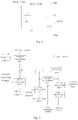
- the pixel driving circuit comprises a light emitting device, a storage capacitor, a driving unit and five switching units; wherein each switching unit comprises a control port, a first signal port and a second signal port; the control port of the switching unit is used for inputting a control signal, thereby turning on or turning off the first signal port and the second signal port;
- the drive unit comprises a control port, a signal input port and a driving port, the control port and the signal input port of the driving unit are used for controlling outputting a driving signal at the driving port;
- a control port of a first switching unit is used for inputting a reset signal;
- a first signal port of the first switching unit is used for inputting an initializing level;
- a control port of a second switching unit is used for inputting a first scanning signal;
- a first signal port of the second switching unit is connected to a second signal port of the first switching unit;
- a first electrode of the storage capacitor is connected
- each of the scanning signals is inputted to a control port of a corresponding switching unit through a scanning line.
- the control port of the second switching unit and the control port of the third switching unit are connected to a same scanning line. It can be understood that scanning signals with a same time sequence can be inputted to the control ports of the switching units if these control ports are connected to a same scanning line.
- each switching unit and each driving unit are indicated with numbers 1, 2 and 3, wherein the control port of each switching unit is port 3, the first signal port is port 1, and the second signal port is port 2; the control port of each driving unit is port 3, the signal input port is port 1, and the driving port is port 2.
- the situation that driving currents of an active light emitting device are affected by threshold voltage shift of a driving transistor can be avoided in a way of voltage compensation, and therefore the evenness of a displayed image is improved.
- An embodiment of the present invention provides a driving method for the pixel driving circuit is provided; the driving method comprises:
- each switching unit the default state of each switching unit is: the first signal port and the second signal port of the switching unit are in offstate.
- the first signal port and the second signal port of the switching unit are switched into turn-on state; therefore, in each phase, except those switching units of which the first signal port and the second signal port are turned on, the first signal port and the second signal port of other switching units are in off-state.
- the driving method for the pixel driving circuit provided by the embodiment of the invention, the situation that driving currents of an active light emitting device are affected by threshold voltage shift of a driving transistor can be avoided in a way of voltage compensation, and therefore the evenness of a displayed image is improved.
- control port of the fifth switching unit and the control port of the fourth switching unit are connected to different scanning lines respectively; and the third scanning signal is not synchronized with the fourth scanning signal.
- the turn-on time sequence of the first signal port and the second signal port of the fourth switching unit is not completely synchronized with the turn-on time sequence of the first signal port and the second signal port of the fifth switching unit; with the control port of the fifth switching unit and the control port of the fourth switching unit being connected to different scanning lines respectively, the inputted third scanning signal is not synchronized with the fourth scanning signal, therefore the fourth switching unit and the fifth switching unit can be controlled respectively, realizing a precise control on the pixel display time; meanwhile, the stability of the light emitting device can also be ensured, it is avoided that a current flows through the light emitting device outside the light emitting phase, prolonging the lifetime of the device.
- the switching units are switching transistors
- the driving unit is a driving transistor.
- the gates of the switching transistors are used as the control ports of the switching units; the sources and the drains of the switching transistors are respectively used as the first signal ports and the second signal ports of the switching units; or, the sources and the drains of the switching transistors are respectively used as the second signal ports and the first signal ports of the switching units.
- the gate of the driving transistor is used as the control port of the driving unit; the source of the driving transistor is used as the signal input port of the driving unit; the drain of the driving transistor is used as the driving port of the driving unit. As shown in Fig.
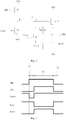
- a pixel driving circuit comprises five switching units (indicated with T1-T5 sequentially), a driving transistor DTFT, and a storage capacitor C1, wherein the storage capacitor comprises a first electrode (connected to node A) and a second electrode (connected to node B).
- all the transistors are for example P type transistors, wherein the first level is a high level VDD, the second level is a low level VSS, the first scanning line Gate provides a scanning signal for T2 and T3, the second scanning line EM1 provides a scanning signal for T5, the third scanning line EM2 provides a scanning signal for T4, the data line Data provides a data signal for the source of T3, Vinit is an initializing level provided when the reset signal Reset is inputted, VDD and VSS are used to power the light emitting device.
- Reset is inputted to the gate of T1, Vinit is inputted to the source of T1, and the drain of T1 is connected to the node A; the gate of T2 is connected to Gate, the source of T2 is connected to the node A, and the drain of T2 is connected to the drain of DTFT; the source of T3 is connected to Data, the gate of T3 is connected to Gate, and the drain of T3 is connected to the node B; VDD is inputted to the source of T4, the gate of T4 is connected to EM2, and drain of T4 is connected to the node B; the gate of T5 is connected to EM1, the source of T5 is connected to the drain of DTFT, the drain of T5 is connected to the first electrode of the light emitting device, and VSS is inputted to the second electrode of the light emitting device; the gate of DTFT is connected to the node A, and VDD is inputted to the source of DTFT.
- the light emitting device can be an active light emitting diode OLED; since the first level is a high level, and the second level is a low level, the OLED can be a bottom emitting OLED; preferably, VSS is grounding.
- the first phase t1 is a pixel initialization phase:
- the second phase t2 is a data writing phase:
- the third phase t3 is a light emitting phase:
- V GS is the voltage between the gate and source of TFT
- ⁇ ⁇ C ox W L
- ⁇ and C ox are constants of the process
- W is the width of the TFT channel
- L is the length of the TFT channel
- both W and L are constants which can be optionally designed.
- the switching transistor and the driving transistor being P type transistor.
- the type of the transistor can be simply replaced, as long as the time sequence state inputted to the corresponding scanning signal line is adjusted accordingly.
- the embodiments of the invention do not limit the type of the switching transistor and driving transistor.
- the type of the switching transistor and driving transistor is changed, only the level signal applied on the gate of the transistor should be adjusted, as long as it can realize the driving method for the pixel driving circuit provided by the embodiments of the invention. Any combination easily occurring to those skilled in the art based on the pixel driving circuit and the driving method provided by the embodiments of the invention should be encompassed within the protection scope of the invention.
- the situation that driving currents of an active light emitting device are affected by threshold voltage shift of a driving transistor can be avoided in a way of voltage compensation, and therefore the evenness of a displayed image is improved.
- An embodiment of the invention also provides a display device, the display device comprising the above mentioned pixel driving circuit.
- the display device can be display equipment such as electronic paper, mobile phone, TV, digital photo frame and so on.
- the situation that driving currents of an active light emitting device are affected by threshold voltage shift of a driving transistor can be avoided in a way of voltage compensation, and therefore the evenness of a displayed image is improved.
Landscapes
- Engineering & Computer Science (AREA)
- Physics & Mathematics (AREA)
- Computer Hardware Design (AREA)
- General Physics & Mathematics (AREA)
- Theoretical Computer Science (AREA)
- Control Of Indicators Other Than Cathode Ray Tubes (AREA)
- Electroluminescent Light Sources (AREA)
- Control Of El Displays (AREA)
Applications Claiming Priority (2)
| Application Number | Priority Date | Filing Date | Title |
|---|---|---|---|
| CN201410190523.7A CN103971640B (zh) | 2014-05-07 | 2014-05-07 | 一种像素驱动电路及其驱动方法和显示装置 |
| PCT/CN2014/084631 WO2015169006A1 (zh) | 2014-05-07 | 2014-08-18 | 一种像素驱动电路及其驱动方法和显示装置 |
Publications (3)
| Publication Number | Publication Date |
|---|---|
| EP3142100A1 true EP3142100A1 (de) | 2017-03-15 |
| EP3142100A4 EP3142100A4 (de) | 2017-11-08 |
| EP3142100B1 EP3142100B1 (de) | 2022-11-09 |
Family
ID=51241063
Family Applications (1)
| Application Number | Title | Priority Date | Filing Date |
|---|---|---|---|
| EP14861171.8A Active EP3142100B1 (de) | 2014-05-07 | 2014-08-18 | Pixelansteuerungsschaltung und ansteuerungsverfahren dafür sowie anzeigevorrichtung |
Country Status (4)
| Country | Link |
|---|---|
| US (1) | US9886898B2 (de) |
| EP (1) | EP3142100B1 (de) |
| CN (1) | CN103971640B (de) |
| WO (1) | WO2015169006A1 (de) |
Families Citing this family (33)
| Publication number | Priority date | Publication date | Assignee | Title |
|---|---|---|---|---|
| CN103971640B (zh) * | 2014-05-07 | 2016-08-24 | 京东方科技集团股份有限公司 | 一种像素驱动电路及其驱动方法和显示装置 |
| CN104240639B (zh) | 2014-08-22 | 2016-07-06 | 京东方科技集团股份有限公司 | 一种像素电路、有机电致发光显示面板及显示装置 |
| CN104464616B (zh) * | 2014-10-28 | 2017-10-03 | 上海天马有机发光显示技术有限公司 | 像素电路及其驱动方法、显示面板 |
| CN104464643B (zh) * | 2014-12-29 | 2017-05-03 | 上海和辉光电有限公司 | 显示装置、像素驱动电路及其驱动方法 |
| CN104575389A (zh) * | 2015-01-29 | 2015-04-29 | 京东方科技集团股份有限公司 | 像素电路及其驱动方法、显示面板及显示装置 |
| CN104599638A (zh) * | 2015-02-12 | 2015-05-06 | 京东方科技集团股份有限公司 | 一种像素电路及其驱动方法和显示装置 |
| CN104658480A (zh) * | 2015-03-06 | 2015-05-27 | 京东方科技集团股份有限公司 | 像素电路及其驱动方法、显示装置 |
| CN104658484B (zh) * | 2015-03-18 | 2018-01-16 | 上海和辉光电有限公司 | 显示装置、像素驱动电路及其驱动方法 |
| KR102652310B1 (ko) * | 2016-08-30 | 2024-03-29 | 엘지디스플레이 주식회사 | 유기발광표시장치, 컨트롤러 및 컨트롤러의 구동 방법 |
| CN106128365B (zh) * | 2016-09-19 | 2018-09-18 | 成都京东方光电科技有限公司 | 像素驱动电路及其驱动方法和显示装置 |
| CN106128366B (zh) * | 2016-09-19 | 2018-10-30 | 成都京东方光电科技有限公司 | 像素驱动电路及其驱动方法和显示装置 |
| US10789891B2 (en) | 2016-09-19 | 2020-09-29 | Boe Technology Group Co., Ltd. | Pixel circuit, driving method thereof, display substrate and display apparatus |
| CN106409227A (zh) * | 2016-12-02 | 2017-02-15 | 武汉华星光电技术有限公司 | 像素电路及其驱动方法和有机发光显示器 |
| CN107346654B (zh) * | 2017-08-29 | 2023-11-28 | 京东方科技集团股份有限公司 | 一种像素电路及其驱动方法、显示装置 |
| CN107846559B (zh) * | 2017-10-09 | 2021-06-15 | 上海集成电路研发中心有限公司 | 一种高动态范围的图像传感器结构及其驱动方法 |
| CN107886901B (zh) * | 2017-12-04 | 2019-10-18 | 合肥鑫晟光电科技有限公司 | 像素驱动电路、显示面板及其驱动方法 |
| US11158257B2 (en) * | 2018-03-19 | 2021-10-26 | Sharp Kabushiki Kaisha | Display device and driving method for same |
| CN110021259B (zh) | 2018-03-23 | 2020-12-22 | 京东方科技集团股份有限公司 | 电源电压提供电路、方法、显示基板和显示装置 |
| CN109119024A (zh) * | 2018-08-28 | 2019-01-01 | 武汉天马微电子有限公司 | 一种驱动电路、驱动方法、显示面板和显示装置 |
| CN109036288B (zh) * | 2018-09-28 | 2020-09-22 | 昆山国显光电有限公司 | 像素电路及其控制方法 |
| CN109192143A (zh) | 2018-09-28 | 2019-01-11 | 昆山国显光电有限公司 | 像素电路及其驱动方法、显示面板、显示装置 |
| CN109872682A (zh) * | 2019-03-28 | 2019-06-11 | 武汉华星光电半导体显示技术有限公司 | 像素补偿电路及显示装置 |
| CN110738964A (zh) * | 2019-10-29 | 2020-01-31 | 京东方科技集团股份有限公司 | 像素电路及显示装置 |
| TWI731462B (zh) * | 2019-11-05 | 2021-06-21 | 友達光電股份有限公司 | 畫素電路、畫素結構與相關的畫素矩陣 |
| JP7414204B2 (ja) * | 2019-11-29 | 2024-01-16 | 京東方科技集團股▲ふん▼有限公司 | 画素駆動回路、その駆動方法及び表示装置 |
| CN111754941B (zh) | 2020-07-29 | 2022-04-15 | 京东方科技集团股份有限公司 | 像素电路及其驱动方法、显示基板和显示装置 |
| WO2022041227A1 (zh) | 2020-08-31 | 2022-03-03 | 京东方科技集团股份有限公司 | 显示面板及显示装置 |
| CN115398523B (zh) * | 2021-01-27 | 2025-08-05 | 京东方科技集团股份有限公司 | 像素驱动电路及其驱动方法、显示基板、显示装置 |
| CN112509523B (zh) * | 2021-02-04 | 2021-05-25 | 上海视涯技术有限公司 | 一种显示面板、驱动方法及显示装置 |
| TWI801080B (zh) * | 2022-01-05 | 2023-05-01 | 友達光電股份有限公司 | 畫素驅動裝置 |
| CN114677947A (zh) * | 2022-03-22 | 2022-06-28 | Tcl华星光电技术有限公司 | 像素电路及显示面板 |
| CN114743491A (zh) * | 2022-04-02 | 2022-07-12 | 昆山国显光电有限公司 | 一种像素驱动电路及其驱动方法、显示面板 |
| CN114639347A (zh) * | 2022-04-27 | 2022-06-17 | 惠科股份有限公司 | 像素驱动电路、驱动方法及显示装置 |
Family Cites Families (10)
| Publication number | Priority date | Publication date | Assignee | Title |
|---|---|---|---|---|
| JP3832415B2 (ja) * | 2002-10-11 | 2006-10-11 | ソニー株式会社 | アクティブマトリクス型表示装置 |
| TWI276029B (en) * | 2005-11-28 | 2007-03-11 | Chi Mei El Corp | Organic light-emitting display and voltage-driven organic light-emitting pixel |
| CN101405785B (zh) * | 2006-05-30 | 2011-08-17 | 夏普株式会社 | 电流驱动型显示装置 |
| KR100846591B1 (ko) * | 2006-12-01 | 2008-07-16 | 삼성에스디아이 주식회사 | 유기전계발광 표시장치 및 이의 구동방법 |
| KR101404549B1 (ko) * | 2008-02-15 | 2014-06-10 | 삼성디스플레이 주식회사 | 표시 장치 및 그 구동 방법 |
| KR101518742B1 (ko) * | 2008-09-19 | 2015-05-11 | 삼성디스플레이 주식회사 | 표시 장치 및 그 구동 방법 |
| KR101058116B1 (ko) * | 2009-12-08 | 2011-08-24 | 삼성모바일디스플레이주식회사 | 화소 회로 및 유기 전계 발광 표시 장치 |
| TWI488348B (zh) * | 2012-05-24 | 2015-06-11 | Au Optronics Corp | 發光二極體顯示器之畫素電路及其驅動方法與發光二極體顯示器 |
| CN103117041A (zh) * | 2013-01-31 | 2013-05-22 | 华南理工大学 | 有源有机电致发光显示器的像素电路及其编程方法 |
| CN103971640B (zh) | 2014-05-07 | 2016-08-24 | 京东方科技集团股份有限公司 | 一种像素驱动电路及其驱动方法和显示装置 |
-
2014
- 2014-05-07 CN CN201410190523.7A patent/CN103971640B/zh active Active
- 2014-08-18 WO PCT/CN2014/084631 patent/WO2015169006A1/zh not_active Ceased
- 2014-08-18 US US14/442,391 patent/US9886898B2/en active Active
- 2014-08-18 EP EP14861171.8A patent/EP3142100B1/de active Active
Also Published As
| Publication number | Publication date |
|---|---|
| US9886898B2 (en) | 2018-02-06 |
| WO2015169006A1 (zh) | 2015-11-12 |
| EP3142100B1 (de) | 2022-11-09 |
| CN103971640B (zh) | 2016-08-24 |
| EP3142100A4 (de) | 2017-11-08 |
| CN103971640A (zh) | 2014-08-06 |
| US20170047002A1 (en) | 2017-02-16 |
Similar Documents
| Publication | Publication Date | Title |
|---|---|---|
| US9886898B2 (en) | Pixel driving circuit, driving method for pixel driving circuit and display device | |
| US10157571B2 (en) | Display panel, method for driving the same and display device | |
| US10339865B2 (en) | Pixel driver circuit having two pixel drivers and display device thereof | |
| US9734763B2 (en) | Pixel circuit, driving method and display apparatus | |
| US9837019B2 (en) | Pixel circuit, organic electroluminescent display panel and display device | |
| US8917224B2 (en) | Pixel unit circuit and OLED display apparatus | |
| CN103198793B (zh) | 像素电路及其驱动方法、显示装置 | |
| US10297195B2 (en) | Pixel circuit and driving method thereof, array substrate, display panel and display device | |
| US9805654B2 (en) | Pixel circuit and its driving method, organic light-emitting display panel and display device | |
| US9355597B2 (en) | Pixel circuit having threshold voltage compensation and method for driving the same | |
| US10545607B2 (en) | Pixel circuit and driving method, display panel and display apparatus | |
| US9514676B2 (en) | Pixel circuit and driving method thereof and display apparatus | |
| US9412302B2 (en) | Pixel driving circuit, driving method, array substrate and display apparatus | |
| CN104167171B (zh) | 一种像素电路和显示装置 | |
| US9437142B2 (en) | Pixel circuit and display apparatus | |
| US20180005570A1 (en) | Pixel circuit, driving method for the pixel circuit, display panel, and display device | |
| US20160300531A1 (en) | Pixel circuit and display apparatus | |
| WO2015192528A1 (zh) | 像素电路和显示装置 | |
| CN106128365B (zh) | 像素驱动电路及其驱动方法和显示装置 | |
| US10510297B2 (en) | Pixel circuit, driving method thereof, display panel and display device | |
| JP5685747B2 (ja) | アクティブマトリクス型表示装置 | |
| WO2016004693A1 (zh) | 像素电路及其驱动方法和显示装置 | |
| US10515591B2 (en) | Pixel driving circuit, driving method thereof, display substrate and display apparatus | |
| US20150145853A1 (en) | Pixel circuit, method for driving the same, array substrate, display device |
Legal Events
| Date | Code | Title | Description |
|---|---|---|---|
| PUAI | Public reference made under article 153(3) epc to a published international application that has entered the european phase |
Free format text: ORIGINAL CODE: 0009012 |
|
| STAA | Information on the status of an ep patent application or granted ep patent |
Free format text: STATUS: REQUEST FOR EXAMINATION WAS MADE |
|
| 17P | Request for examination filed |
Effective date: 20150520 |
|
| AK | Designated contracting states |
Kind code of ref document: A1 Designated state(s): AL AT BE BG CH CY CZ DE DK EE ES FI FR GB GR HR HU IE IS IT LI LT LU LV MC MK MT NL NO PL PT RO RS SE SI SK SM TR |
|
| AX | Request for extension of the european patent |
Extension state: BA ME |
|
| DAX | Request for extension of the european patent (deleted) | ||
| A4 | Supplementary search report drawn up and despatched |
Effective date: 20171010 |
|
| RIC1 | Information provided on ipc code assigned before grant |
Ipc: G09G 3/3233 20160101AFI20171004BHEP Ipc: G09G 3/3291 20160101ALN20171004BHEP |
|
| STAA | Information on the status of an ep patent application or granted ep patent |
Free format text: STATUS: EXAMINATION IS IN PROGRESS |
|
| 17Q | First examination report despatched |
Effective date: 20191108 |
|
| REG | Reference to a national code |
Ref country code: DE Ref legal event code: R079 Ref document number: 602014085505 Country of ref document: DE Free format text: PREVIOUS MAIN CLASS: G09G0003320000 Ipc: G09G0003323300 |
|
| GRAP | Despatch of communication of intention to grant a patent |
Free format text: ORIGINAL CODE: EPIDOSNIGR1 |
|
| STAA | Information on the status of an ep patent application or granted ep patent |
Free format text: STATUS: GRANT OF PATENT IS INTENDED |
|
| RIC1 | Information provided on ipc code assigned before grant |
Ipc: G09G 3/3291 20160101ALN20220530BHEP Ipc: G09G 3/3233 20160101AFI20220530BHEP |
|
| INTG | Intention to grant announced |
Effective date: 20220617 |
|
| RIC1 | Information provided on ipc code assigned before grant |
Ipc: G09G 3/3291 20160101ALN20220603BHEP Ipc: G09G 3/3233 20160101AFI20220603BHEP |
|
| GRAS | Grant fee paid |
Free format text: ORIGINAL CODE: EPIDOSNIGR3 |
|
| GRAA | (expected) grant |
Free format text: ORIGINAL CODE: 0009210 |
|
| STAA | Information on the status of an ep patent application or granted ep patent |
Free format text: STATUS: THE PATENT HAS BEEN GRANTED |
|
| AK | Designated contracting states |
Kind code of ref document: B1 Designated state(s): AL AT BE BG CH CY CZ DE DK EE ES FI FR GB GR HR HU IE IS IT LI LT LU LV MC MK MT NL NO PL PT RO RS SE SI SK SM TR |
|
| REG | Reference to a national code |
Ref country code: GB Ref legal event code: FG4D |
|
| REG | Reference to a national code |
Ref country code: CH Ref legal event code: EP Ref country code: AT Ref legal event code: REF Ref document number: 1530902 Country of ref document: AT Kind code of ref document: T Effective date: 20221115 |
|
| REG | Reference to a national code |
Ref country code: DE Ref legal event code: R096 Ref document number: 602014085505 Country of ref document: DE |
|
| REG | Reference to a national code |
Ref country code: IE Ref legal event code: FG4D |
|
| REG | Reference to a national code |
Ref country code: LT Ref legal event code: MG9D |
|
| REG | Reference to a national code |
Ref country code: NL Ref legal event code: MP Effective date: 20221109 |
|
| REG | Reference to a national code |
Ref country code: AT Ref legal event code: MK05 Ref document number: 1530902 Country of ref document: AT Kind code of ref document: T Effective date: 20221109 |
|
| PG25 | Lapsed in a contracting state [announced via postgrant information from national office to epo] |
Ref country code: SE Free format text: LAPSE BECAUSE OF FAILURE TO SUBMIT A TRANSLATION OF THE DESCRIPTION OR TO PAY THE FEE WITHIN THE PRESCRIBED TIME-LIMIT Effective date: 20221109 Ref country code: PT Free format text: LAPSE BECAUSE OF FAILURE TO SUBMIT A TRANSLATION OF THE DESCRIPTION OR TO PAY THE FEE WITHIN THE PRESCRIBED TIME-LIMIT Effective date: 20230309 Ref country code: NO Free format text: LAPSE BECAUSE OF FAILURE TO SUBMIT A TRANSLATION OF THE DESCRIPTION OR TO PAY THE FEE WITHIN THE PRESCRIBED TIME-LIMIT Effective date: 20230209 Ref country code: LT Free format text: LAPSE BECAUSE OF FAILURE TO SUBMIT A TRANSLATION OF THE DESCRIPTION OR TO PAY THE FEE WITHIN THE PRESCRIBED TIME-LIMIT Effective date: 20221109 Ref country code: FI Free format text: LAPSE BECAUSE OF FAILURE TO SUBMIT A TRANSLATION OF THE DESCRIPTION OR TO PAY THE FEE WITHIN THE PRESCRIBED TIME-LIMIT Effective date: 20221109 Ref country code: ES Free format text: LAPSE BECAUSE OF FAILURE TO SUBMIT A TRANSLATION OF THE DESCRIPTION OR TO PAY THE FEE WITHIN THE PRESCRIBED TIME-LIMIT Effective date: 20221109 Ref country code: AT Free format text: LAPSE BECAUSE OF FAILURE TO SUBMIT A TRANSLATION OF THE DESCRIPTION OR TO PAY THE FEE WITHIN THE PRESCRIBED TIME-LIMIT Effective date: 20221109 |
|
| PG25 | Lapsed in a contracting state [announced via postgrant information from national office to epo] |
Ref country code: RS Free format text: LAPSE BECAUSE OF FAILURE TO SUBMIT A TRANSLATION OF THE DESCRIPTION OR TO PAY THE FEE WITHIN THE PRESCRIBED TIME-LIMIT Effective date: 20221109 Ref country code: PL Free format text: LAPSE BECAUSE OF FAILURE TO SUBMIT A TRANSLATION OF THE DESCRIPTION OR TO PAY THE FEE WITHIN THE PRESCRIBED TIME-LIMIT Effective date: 20221109 Ref country code: LV Free format text: LAPSE BECAUSE OF FAILURE TO SUBMIT A TRANSLATION OF THE DESCRIPTION OR TO PAY THE FEE WITHIN THE PRESCRIBED TIME-LIMIT Effective date: 20221109 Ref country code: IS Free format text: LAPSE BECAUSE OF FAILURE TO SUBMIT A TRANSLATION OF THE DESCRIPTION OR TO PAY THE FEE WITHIN THE PRESCRIBED TIME-LIMIT Effective date: 20230309 Ref country code: HR Free format text: LAPSE BECAUSE OF FAILURE TO SUBMIT A TRANSLATION OF THE DESCRIPTION OR TO PAY THE FEE WITHIN THE PRESCRIBED TIME-LIMIT Effective date: 20221109 Ref country code: GR Free format text: LAPSE BECAUSE OF FAILURE TO SUBMIT A TRANSLATION OF THE DESCRIPTION OR TO PAY THE FEE WITHIN THE PRESCRIBED TIME-LIMIT Effective date: 20230210 |
|
| PG25 | Lapsed in a contracting state [announced via postgrant information from national office to epo] |
Ref country code: NL Free format text: LAPSE BECAUSE OF FAILURE TO SUBMIT A TRANSLATION OF THE DESCRIPTION OR TO PAY THE FEE WITHIN THE PRESCRIBED TIME-LIMIT Effective date: 20221109 |
|
| PG25 | Lapsed in a contracting state [announced via postgrant information from national office to epo] |
Ref country code: SM Free format text: LAPSE BECAUSE OF FAILURE TO SUBMIT A TRANSLATION OF THE DESCRIPTION OR TO PAY THE FEE WITHIN THE PRESCRIBED TIME-LIMIT Effective date: 20221109 Ref country code: RO Free format text: LAPSE BECAUSE OF FAILURE TO SUBMIT A TRANSLATION OF THE DESCRIPTION OR TO PAY THE FEE WITHIN THE PRESCRIBED TIME-LIMIT Effective date: 20221109 Ref country code: EE Free format text: LAPSE BECAUSE OF FAILURE TO SUBMIT A TRANSLATION OF THE DESCRIPTION OR TO PAY THE FEE WITHIN THE PRESCRIBED TIME-LIMIT Effective date: 20221109 Ref country code: DK Free format text: LAPSE BECAUSE OF FAILURE TO SUBMIT A TRANSLATION OF THE DESCRIPTION OR TO PAY THE FEE WITHIN THE PRESCRIBED TIME-LIMIT Effective date: 20221109 Ref country code: CZ Free format text: LAPSE BECAUSE OF FAILURE TO SUBMIT A TRANSLATION OF THE DESCRIPTION OR TO PAY THE FEE WITHIN THE PRESCRIBED TIME-LIMIT Effective date: 20221109 |
|
| REG | Reference to a national code |
Ref country code: DE Ref legal event code: R097 Ref document number: 602014085505 Country of ref document: DE |
|
| PG25 | Lapsed in a contracting state [announced via postgrant information from national office to epo] |
Ref country code: SK Free format text: LAPSE BECAUSE OF FAILURE TO SUBMIT A TRANSLATION OF THE DESCRIPTION OR TO PAY THE FEE WITHIN THE PRESCRIBED TIME-LIMIT Effective date: 20221109 Ref country code: AL Free format text: LAPSE BECAUSE OF FAILURE TO SUBMIT A TRANSLATION OF THE DESCRIPTION OR TO PAY THE FEE WITHIN THE PRESCRIBED TIME-LIMIT Effective date: 20221109 |
|
| PLBE | No opposition filed within time limit |
Free format text: ORIGINAL CODE: 0009261 |
|
| STAA | Information on the status of an ep patent application or granted ep patent |
Free format text: STATUS: NO OPPOSITION FILED WITHIN TIME LIMIT |
|
| 26N | No opposition filed |
Effective date: 20230810 |
|
| PG25 | Lapsed in a contracting state [announced via postgrant information from national office to epo] |
Ref country code: SI Free format text: LAPSE BECAUSE OF FAILURE TO SUBMIT A TRANSLATION OF THE DESCRIPTION OR TO PAY THE FEE WITHIN THE PRESCRIBED TIME-LIMIT Effective date: 20221109 |
|
| PG25 | Lapsed in a contracting state [announced via postgrant information from national office to epo] |
Ref country code: MC Free format text: LAPSE BECAUSE OF FAILURE TO SUBMIT A TRANSLATION OF THE DESCRIPTION OR TO PAY THE FEE WITHIN THE PRESCRIBED TIME-LIMIT Effective date: 20221109 |
|
| REG | Reference to a national code |
Ref country code: CH Ref legal event code: PL |
|
| PG25 | Lapsed in a contracting state [announced via postgrant information from national office to epo] |
Ref country code: MC Free format text: LAPSE BECAUSE OF FAILURE TO SUBMIT A TRANSLATION OF THE DESCRIPTION OR TO PAY THE FEE WITHIN THE PRESCRIBED TIME-LIMIT Effective date: 20221109 |
|
| PG25 | Lapsed in a contracting state [announced via postgrant information from national office to epo] |
Ref country code: LU Free format text: LAPSE BECAUSE OF NON-PAYMENT OF DUE FEES Effective date: 20230818 |
|
| GBPC | Gb: european patent ceased through non-payment of renewal fee |
Effective date: 20230818 |
|
| PG25 | Lapsed in a contracting state [announced via postgrant information from national office to epo] |
Ref country code: LU Free format text: LAPSE BECAUSE OF NON-PAYMENT OF DUE FEES Effective date: 20230818 Ref country code: CH Free format text: LAPSE BECAUSE OF NON-PAYMENT OF DUE FEES Effective date: 20230831 |
|
| REG | Reference to a national code |
Ref country code: BE Ref legal event code: MM Effective date: 20230831 |
|
| REG | Reference to a national code |
Ref country code: IE Ref legal event code: MM4A |
|
| PG25 | Lapsed in a contracting state [announced via postgrant information from national office to epo] |
Ref country code: IT Free format text: LAPSE BECAUSE OF FAILURE TO SUBMIT A TRANSLATION OF THE DESCRIPTION OR TO PAY THE FEE WITHIN THE PRESCRIBED TIME-LIMIT Effective date: 20221109 |
|
| PG25 | Lapsed in a contracting state [announced via postgrant information from national office to epo] |
Ref country code: IE Free format text: LAPSE BECAUSE OF NON-PAYMENT OF DUE FEES Effective date: 20230818 |
|
| PG25 | Lapsed in a contracting state [announced via postgrant information from national office to epo] |
Ref country code: GB Free format text: LAPSE BECAUSE OF NON-PAYMENT OF DUE FEES Effective date: 20230818 |
|
| PG25 | Lapsed in a contracting state [announced via postgrant information from national office to epo] |
Ref country code: IE Free format text: LAPSE BECAUSE OF NON-PAYMENT OF DUE FEES Effective date: 20230818 Ref country code: GB Free format text: LAPSE BECAUSE OF NON-PAYMENT OF DUE FEES Effective date: 20230818 Ref country code: FR Free format text: LAPSE BECAUSE OF NON-PAYMENT OF DUE FEES Effective date: 20230831 |
|
| PG25 | Lapsed in a contracting state [announced via postgrant information from national office to epo] |
Ref country code: BE Free format text: LAPSE BECAUSE OF NON-PAYMENT OF DUE FEES Effective date: 20230831 |
|
| PG25 | Lapsed in a contracting state [announced via postgrant information from national office to epo] |
Ref country code: BG Free format text: LAPSE BECAUSE OF FAILURE TO SUBMIT A TRANSLATION OF THE DESCRIPTION OR TO PAY THE FEE WITHIN THE PRESCRIBED TIME-LIMIT Effective date: 20221109 |
|
| PG25 | Lapsed in a contracting state [announced via postgrant information from national office to epo] |
Ref country code: BG Free format text: LAPSE BECAUSE OF FAILURE TO SUBMIT A TRANSLATION OF THE DESCRIPTION OR TO PAY THE FEE WITHIN THE PRESCRIBED TIME-LIMIT Effective date: 20221109 |
|
| PG25 | Lapsed in a contracting state [announced via postgrant information from national office to epo] |
Ref country code: CY Free format text: LAPSE BECAUSE OF FAILURE TO SUBMIT A TRANSLATION OF THE DESCRIPTION OR TO PAY THE FEE WITHIN THE PRESCRIBED TIME-LIMIT; INVALID AB INITIO Effective date: 20140818 |
|
| PG25 | Lapsed in a contracting state [announced via postgrant information from national office to epo] |
Ref country code: HU Free format text: LAPSE BECAUSE OF FAILURE TO SUBMIT A TRANSLATION OF THE DESCRIPTION OR TO PAY THE FEE WITHIN THE PRESCRIBED TIME-LIMIT; INVALID AB INITIO Effective date: 20140818 |
|
| PGFP | Annual fee paid to national office [announced via postgrant information from national office to epo] |
Ref country code: DE Payment date: 20250820 Year of fee payment: 12 |
|
| PG25 | Lapsed in a contracting state [announced via postgrant information from national office to epo] |
Ref country code: TR Free format text: LAPSE BECAUSE OF FAILURE TO SUBMIT A TRANSLATION OF THE DESCRIPTION OR TO PAY THE FEE WITHIN THE PRESCRIBED TIME-LIMIT Effective date: 20221109 |