EP3143720B1 - Contre-mesures d'analyse de puissance différentielle - Google Patents
Contre-mesures d'analyse de puissance différentielle Download PDFInfo
- Publication number
- EP3143720B1 EP3143720B1 EP15809894.7A EP15809894A EP3143720B1 EP 3143720 B1 EP3143720 B1 EP 3143720B1 EP 15809894 A EP15809894 A EP 15809894A EP 3143720 B1 EP3143720 B1 EP 3143720B1
- Authority
- EP
- European Patent Office
- Prior art keywords
- logic
- input
- value
- logic unit
- processing
- Prior art date
- Legal status (The legal status is an assumption and is not a legal conclusion. Google has not performed a legal analysis and makes no representation as to the accuracy of the status listed.)
- Active
Links
Images


Classifications
-
- H—ELECTRICITY
- H04—ELECTRIC COMMUNICATION TECHNIQUE
- H04L—TRANSMISSION OF DIGITAL INFORMATION, e.g. TELEGRAPHIC COMMUNICATION
- H04L9/00—Cryptographic mechanisms or cryptographic arrangements for secret or secure communications; Network security protocols
- H04L9/002—Countermeasures against attacks on cryptographic mechanisms
- H04L9/003—Countermeasures against attacks on cryptographic mechanisms for power analysis, e.g. differential power analysis [DPA] or simple power analysis [SPA]
-
- H—ELECTRICITY
- H04—ELECTRIC COMMUNICATION TECHNIQUE
- H04L—TRANSMISSION OF DIGITAL INFORMATION, e.g. TELEGRAPHIC COMMUNICATION
- H04L2209/00—Additional information or applications relating to cryptographic mechanisms or cryptographic arrangements for secret or secure communication H04L9/00
- H04L2209/08—Randomization, e.g. dummy operations or using noise
Definitions
- the present disclosure relates to cryptographic devices.
- An electronic device may comprise a secure, embedded system (e.g., hardware and/or software) that protects sensitive data utilized by the electronic device according to encryption standards.
- an electronic device e.g., a smart card, mobile device, television unit, etc.
- Encryption or decryption may be in accordance with the Advanced Encryption Standard (AES), a Data Encryption Standard (DES) or other cyphers.
- AES Advanced Encryption Standard
- DES Data Encryption Standard
- Cryptography typically use keys to encrypt and decrypt data, and these keys are generally known only to the device(s) performing the cryptographic techniques. It is important to ensure that these keys are not easily detectable by unauthorized people including computer hackers and cyber attackers.
- US 2009/092245 discloses a cryptographic mechanism that offers resistance to side channel attacks by incorporating a specific type of masking mechanism.
- US 2002/172357 discloses a device having multiple processing stages arranged in a circular manner so that data is repeatedly passed from a prior stage to a next stage, and from a last stage back to a first stage, until processing is completed.
- the use of one or more registers at one or more positions between the processing stages allows data to be stored so that the stream associated with the stored data can effectively be suspended. This allows data from another stream to be processed while the suspended stream is in a wait state.
- Embodiments described hereinbelow provide an electronic device, comprising a plurality of logic units, which are arranged in a ring topology.
- ring topology means that the input of each of the logic units is coupled to the output of another of the logic units.
- Each of the logic units comprises respective processing logic, which is identical to and operates in synchrony with the processing logic of the other logic units.
- the processing logic in each of the logic units processes, at each cycle, a respective data value using at least one secret value stored in the device.
- the logic units receive different, respective input values that are mutually uncorrelated.
- each of the logic units receives and operates on an intermediate value that has been output by another of the logic units, until an output value is generated after a certain number of cycles.
- the electronic device comprises a device input, which is coupled to receive a first input value, and a device output.
- a logic core comprising at least first and second logic units, is coupled to the device input so as to receive and process this first input value and, ultimately, to provide the output value at the device output.
- the logic core comprises an input generator, which provides at least one second input value that is uncorrelated with the first input value, and is typically inaccessible outside the device.
- the first logic unit comprises a first logic input, which is coupled to receive the first input value from the device input, and first processing logic configured to operate on first data values provided by the first logic input using the secret value.
- the second logic unit comprises a second logic input, which is coupled to receive the second input value from the input generator, and second processing logic identical to the first processing logic and configured to operate, in synchrony with the first processing logic, on second data values provided by the second logic input.
- the use of the two (or more) logic units in a ring topology to process different, uncorrelated values synchronously, using identical processing logic, as provided by the disclosed embodiments, is useful in foiling attacks based on differential power analysis (DPA). Because only the first input value can be chosen externally, any relationship between the chosen input value and power consumption due to bit transitions in one of the logic units will be masked by the interleaving of uncorrelated values due to the other input values. Therefore, the attacker's attempts to find a correlation between input values and power consumption, and thus find the secret value held in the device, will fail.
- DPA differential power analysis
- the input generator comprises a random data generator, such that the second input value is a random value.
- the second input value is a random value.
- other sources of second input values may be used, as long as they are uncorrelated with the first input value and inaccessible to attackers.
- the output of each logic unit feeds the input of another logic unit.
- the second logic input is coupled to receive the second input value at an initial cycle of the device and to receive, at subsequent cycles of the device, first intermediate values generated by the first processing logic for processing by the second processing logic.
- the first logic input may be coupled to receive the first input value at the initial cycle of the device and to receive, at the subsequent cycles of the device, second intermediate values generated by the second processing logic for processing by the first processing logic.
- a third logic unit comprising a third logic input, is coupled to receive second intermediate values generated by the second processing logic.
- Third processing logic identical to the first and second processing logic, is configured to operate, in synchrony with the first and second processing logic, on third data values provided by the third logic input.
- the first logic input may be coupled to receive the first input value at the initial cycle of the device and to receive, at the subsequent cycles of the device, third intermediate values generated by the third processing logic for processing by the first processing logic.
- the second processing logic (and processing logic in other logic units, if present) may be configured to operate on the second data values using the same secret value as the first processing logic or using another secret value, different from the secret value used by the first processing logic.
- the techniques presented herein relate to enhanced encryption and decryption for cryptographic devices.
- these techniques enable enhanced cryptography for cryptographic devices.
- cryptographic device defines an electronic device that is configured to perform encryption operations and/or decryption operations (referred to generally as “cryptographic operations"). After receiving the input data, a cryptographic device may encrypt the input data and generate as output data cipher data, also referred to as "cipher text.” Alternatively or additionally, a cryptographic device may receive cipher text and decrypt the cipher text to generate the original input data.
- encryption operations referred to generally as “cryptographic operations”
- the cryptographic device performs encryption and/or decryption techniques by utilizing an encryption/decryption algorithm and a secret key (referred to hereinafter as a "key").
- a secret key referred to hereinafter as a "key”
- the key is used by the cryptographic device to cipher or encrypt the input data in accordance with an encryption algorithm to create the cipher text.
- the key is used by the cryptographic device to decipher or decrypt the cipher text in accordance with a decryption algorithm.
- the key may be a 256 bit (32 byte) key that is configured to perform the encryption and/or decryption operations in accordance with an encryption/decryption algorithm (also referred to hereinafter as "algorithm” for simplicity).
- Examples of algorithms include the Advanced Encryption Standard (AES), Data Encryption Standard (DES), etc.
- AES Advanced Encryption Standard
- DES Data Encryption Standard
- the input data is received by the cryptographic device, and the key is used to encrypt the input data using an algorithm.
- the cryptographic device outputs the cipher text after the encryption, and the cipher text is an encrypted version of the input data.
- the input data may be, for example, a 32 byte input and the cipher text may be a 32 byte encrypted version of the input data.
- the cipher text is received by the cryptographic device, and the key is used to decrypt the cipher text using a cryptographic algorithm, e.g., AES or DES. After decrypting the cipher text, the cryptographic device outputs the original input data.
- AES Advanced Encryption Standard
- DES Data Encryption Standard
- the key is an important aspect of maintaining the security of the cryptographic operations performed by the cryptographic device.
- the outside party in order for an outside party to undermine the encryption/decryption techniques performed by the cryptographic device, the outside party must know the key and the algorithm used by the cryptographic device.
- the algorithm used by the cryptographic device is known or easy to guess or readily available.
- the cryptographic device may use AES or DES as the cryptographic algorithm, and the definition of the AES and DES algorithms may be publically available to the outside party. Because the key is not publically available to the outside party, even if the outside party has information about the type of cryptography being performed, the outside party is unable to decrypt the cipher text and cannot encrypt the input data.
- the secrecy of the key is essential for maintaining the security of the encryption and decryption operations.
- An outside party may target the cryptographic device to attempt to obtain or learn a key contained therein.
- the attacker may use several techniques to try to obtain the key of the cryptographic device.
- the key may be a 256 bit key, and the attacker may attempt to use a "brute force” technique to guess the correct key value.
- this "brute force” approach would be computationally difficult for the attacker, as the attacker would have to guess the correct 256 bit key combination out of 2 256 possibilities.
- the attacker may attempt to guess the key in bit segments.
- the attacker may attempt to guess the key in 8-bit segments (e.g., key bytes), thereby reducing the number of possibilities to 8192 (2 8 * (256/8)). From the attacker's perspective, it is advantageous to attempt to guess the key in bit segments, as the number of possible samples is significantly less than the brute force approach.
- 8-bit segments e.g., key bytes
- the attacker can supply input data to the cryptographic device, and the attacker can measure the power dissipated by the cryptographic device as the cryptographic device performs the cryptographic operations.
- the cryptographic device comprises integrated circuits which are built out of individual transistors.
- the transistors e.g., operate as voltage-controlled switches and current flows across the transistors when electrical charge is applied to or removed from the gates of the transistors. The current then delivers electrical charge to the gates of other transistors, interconnections and other circuit loads.
- the motion of the electric charge consumes power and produces electromagnetic radiation, both of which are detectable by an outside entity.
- the attacker can measure electrical behaviors of the cryptographic device such as the power dissipated by the cryptographic device over time (e.g., over a period of clock cycles) as the cryptographic device performs the cryptographic operations. The attacker can utilize these measurements to attempt to determine the key of the cryptographic device.
- the hardware design of the cryptographic device includes, e.g., data registers, commonly implemented as flip-flop arrays, and other logical elements.
- the logical elements perform logical operations on data.
- the logical elements may perform a sequence of logical operations such as "AND,” “OR,” “XOR,” etc. operations.
- a series of logical elements is referred to as "combinational logic.” Every combinational logic receives its inputs from flip-flop array(s) that are used to store data, and the output of a combinational logic at every clock cycle is stored to flip-flop arrays.
- a combinational logic together with an input flip-flop array is referred to hereinafter as a "logic unit” or a “multi-state logic unit.”
- the cryptographic device may have one or more logic units.
- the cryptographic device may have two or more logic units that are identical copies of each other and that are logically equivalent. These logic units provide enhanced cryptography for the cryptographic device, as described by the techniques herein.
- the input data is modified in a logic unit by one of the combinational logic of the cryptographic device and stored to flip-flop arrays as a part of a cryptographic operation (e.g., encryption).
- a cryptographic operation e.g., encryption
- the input data is modified (as a part of the cryptographic operation) in a first logic unit by a first one of the combinational logic and stored in a first set of flip-flop arrays
- the modified input data is sent from the first logic unit to a second logic unit and is modified in the second logic unit by a second combinational logic and stored in a second set of flip-flop arrays as a part of the cryptographic operation.
- one or more gates of the devices in the combinational logic may change state.
- gates of one or more devices in the combinational logic may change its state from an "off” state to an “on” state or more simply, from a "0" state to a "1" state.
- the cryptographic device consumes power.
- a power consumption profile (e.g., "power profile") of the cryptographic device.
- the power profile of the cryptographic device describes the power consumption of the cryptographic device over a period of time (e.g., over a period of clock cycles) for a given input.
- An outside entity such as an attacker, supplies input data ("input data A") to the cryptographic device and the attacker measures the power consumed by the cryptographic device over a period of clock cycles to obtain a power profile ("power profile A").
- Power profile A comprises a series of power measurements at different time intervals that correspond to clock cycles of the cryptographic device.
- the cryptographic device when the cryptographic device performs an encryption/decryption operation on input data A, the cryptographic device consumes a certain amount of power over time, represented by power profile A, that can be measured by the attacker.
- Power profile A is unique to the input data, and different input data will result in different power profiles.
- the attacker may supply another input data ("input data B") to obtain another power profile ("power profile B”), and so on.
- input data B another input data
- power profile B another power profile
- the attacker can attempt to guess the key of the cryptographic device using power analysis techniques. For example, the attacker can assume that the overall power consumption of the cryptographic device is related to the number of gates that change in a combinational logic during a cryptographic operation.
- SPA Simple Power Analysis
- the attacker analyzes the power profiles and assumes that the amount of power consumed by the cryptographic device varies depending on the microprocessor instructions performed by the cryptographic device. In other words, the attacker may identify from the power profiles features of AES operations by assuming that different encryption/decryption operations consume different amounts of power. For example, the attacker may use the SPA analysis to reveal differences between multiplication and squaring operations performed by the cryptographic device to perform the encryption/decryption techniques.
- the attacker who uses SPA to attempt to obtain the key relies on visual inspection of the power profiles to identify relevant power fluctuations. SPA attacks, therefore, can be deterred by adding noise to the power profiles.
- DPA Differential Power Analysis
- DPA attacks are more powerful than SPA attacks since random noise alone in the power profiles may not undermine a DPA attack.
- DPA attacks are more time-consuming than SPA attacks.
- the attacker supplies a series of input data and obtains a corresponding series of power profiles.
- the attacker attempts to guess the key of the cryptographic device by guessing segments of the key at a time. For ease of explanation, in this example, the attacker may guess the key in 8-bit segments at a time.
- the attacker makes several assumptions when performing the DPA attack. First, the attacker assumes that the cryptographic device is using a particular cryptographic standard, for example, AES. Additionally, the attacker assumes a particular value for the 8-bit segment of the key that the attacker is attempting to determine.
- the attacker when attempting to use DPA to obtain a key, the attacker assumes that the cryptographic device is performing AES encryption and also assumes a first value for the 8-bit key segment of interest.
- the attacker uses the assumed value of the 8-bit key segment, and based on the assumed AES encryption standard, for every given input data, the attacker is able to simulate a part of the expected intermediate results of an encryption operation performed by the cryptographic device. That is, for every input, the attacker can simulate expected partial intermediate outcomes that would result if the input undergoes AES encryption using the assumed 8-bit key value.
- the expected partial intermediate outcomes are called "intermediate values," and these outcomes are intermediate results of a simulated AES encryption on the input with the assumed 8-bit key value.
- Table 1 shows an example list of simulated expected outcomes of the AES encryption with the assumed 8-bit key value.
- Table 1 Simulated AES encryption with intermediate results for a first assumed key value
- z 5 S(y 5 ) Hamming Distance (y 5 ,z 5 ) 1 0x38 0x2F 0x15 4 2 0x85 0x92 0x4F 6 3 0xE7 0xF0 0x8C 5 ... ... ... ... ... ... ... ... ...
- the attacker may be attempting to determine the fifth byte of the key (e.g., the fifth 8-bit key segment).
- the attacker assumes that at some clock cycle the input to the S-box (marked as y 5 in Table 1) is at some gates, and the output from the S-box (marked as z 5 in Table 1) is at the same gates at the next clock cycle, and thus the values in Table 1 reflect the relevant portions of the AES encryption that are simulated by the attacker to try and determine the fifth byte of the key. All of the simulated outcomes shown in Table 1 are for the same key value assumption for the fifth byte of the key. In other words, the attacker assumes that the fifth byte of the key has some value (that the attacker guesses), and the attacker simulates a series of AES encryptions for this key value assumption. Table 1 shows the simulated AES encryption for a guessed fifth byte key value k 5 .
- the attacker then makes another guess for the fifth byte of the key, and runs another simulation based on this assumption. Ultimately, the attacker attempts to determine which key value assumption is correct. By repeating this analysis for all of the bytes of the key, the attacker can ultimately obtain the entire key of the cryptographic device.
- the input data of the first experiment is shown at value "x 5 " to represent a fifth byte of the overall input data.
- the value x 5 is shown, in an example, as a hexadecimal value "0x38,” which corresponds to the binary value "00111000,” as one with ordinary skill in the art will recognize. Since the attacker knows the input value x 5 (since he provides it), and since the attacker is assuming that the cryptographic device is performing AES encryption, the attacker can simulate intermediate values y 5 and z 5 for the key byte assumption k 5 . For example, in AES encryption, the x 5 byte of the input data may be XORed with the fifth byte of the key of the cryptographic device (shown as k 5 in Table 1).
- the attacker makes an assumption for the key value of k 5 , and thus, the attacker is able to simulate the values of the XOR operation to determine the expected intermediate value y 5 for the given input x 5 .
- the intermediate value y 5 is shown as a hexadecimal value "0x2F,” which corresponds to the binary value "00101111.”
- the attacker is also able to determine the expected intermediate value z 5 which may result under AES, for example, from a byte-to-byte "S-box" function on y 5 .
- the intermediate value z 5 is shown, in an example, as hexadecimal value "0x15,” which corresponds to binary value "00010101.”
- the attacker knows the input data x 5 (that he supplies to the cryptographic device), and the attacker can generate the intermediate values y 5 and z 5 of an AES encryption operation for an assumed key value k 5 (that he assumes).
- the attacker can also calculate a Hamming distance between the intermediate value y 5 and the intermediate value z 5 .
- the Hamming distance between the intermediate values represents the number of bits that are different between z 5 and y 5 .
- the Hamming distance between the intermediate value y 5 and the intermediate value z 5 is four (i.e., the number of bits that are different between "00101111” and "00010101").
- the attacker repeats this process for different input data and obtains a series of results corresponding to different input data.
- the attacker can obtain n Hamming distance values.
- Each of the Hamming distance values corresponds to the number bits that are different between intermediate values y 5 and z 5 for each given input.
- These n Hamming distance values correspond to a single key assumption for k 5 , and as stated above, the attacker will perform different simulations for different key assumptions that he makes for k 5 .
- the attacker can obtain a series of n Hamming distance values, each of which corresponds to a particular input data.
- the attacker will attempt to verify whether or not the key assumption k 5 for the series of input data is correct.
- the attacker assumes that the power consumption during a clock cycle is correlated to the number of gates that have changed their state in the cryptographic device.
- the attacker assumes that the cryptographic device is performing a cryptographic operation using a combinational logic, and the attacker assumes that the power consumption of the cryptographic device is correlated to the Hamming distance between the states of the gates in the combinational logic before and after a clock cycle.
- the attacker assumes, for example, that at one clock cycle, the gates in a combinational logic of a first logic unit are in one set of states to perform the cryptographic operation at that clock cycle, and at a second clock cycle the gates in the same combinational logic are in another set of states to perform the cryptographic operation at that next clock cycle.
- another (identical) combinational logic of a second logic unit may be performing the cryptographic operation instead of the initial logic unit, while the calculations at the same gates in the initial combinational logic pertain to another calculation with inputs unknown to the attacker.
- the number of gates that change in the initial combinational logic of the first logic unit at consecutive clock cycles may not be correlated to Hamming distance values. That is, the attacker assumes that the intermediate values represent intermediate values in the same combinational logic at consecutive clock values.
- the attacker has n Hamming distance values for the n input data that represent the differences between intermediate values, and thus the attacker attempts to use the Hamming distance measurements to determine whether or not it is correlated with the power consumption at consecutive clock cycles.
- Table 2 For example, as shown in Table 2 below, for every key segment assumption, the attacker may generate an n x m table.
- the rows in Table 2 represent each of the n inputs for the given key segment assumption.
- the columns in Table 2 represent power measurements at a particular clock cycle.
- Each entry in Table 2 represents a power consumption measurement obtained by the attacker.
- the entry P n,m represents the power consumed by the cryptographic device for input n at clock cycle m.
- the attacker can generate (by offline calculation) a Hamming distance value between intermediate values of an assumed encryption technique.
- Table 3 Hamming Distance for key segment k 5 showing power profile for each of n inputs for m clock cycles Input Hamming Distance Input 1 H 1 Input 2 H 2 Input 3 H 3 Input n H n
- Each value in Table 3 represents a Hamming distance calculation between intermediate values for a given input.
- the attacker may generate an n x 1 array of Hamming distances for every key segment assumption. As stated above, the attacker may attempt to verify the accuracy of a key segment guess by correlating Hamming distance values with power measurements.
- the attacker assumes in Table 2 that a power value at a given clock cycle represents how many gates have changed state in a combinational logic from an immediately prior clock cycle. Thus, for example, at clock cycle 2 for input 1, the attacker assumes that the intermediate value y 5 appears in a first combinational logic and that the intermediate value z 5 appears in the same combinational logic.
- the attacker assumes that the power value P 1,2 is related to how many gates have changed in the first combinational logic from the immediately prior clock cycle (e.g., clock cycle 1). In other words, the attacker assumes that the power value P 1,2 is related to the Hamming distance between y 5 and z 5 . Since the attacker has n power measurements for clock cycle 2, and since the attacker has n Hamming distance values (for each of the n inputs, as shown in Table 3), the attacker performs a correlation between the n x 1 Hamming distance array in Table. 3 and the n x 1 column representing clock cycle 2.
- the attacker knows that the guessed key portion k 5 is correct. If any of the correlation values are statistically significant, the attacker knows that the guessed key portion k 5 is correct. If the correlation between the n x 1 Hamming distance array and the n x 1 column representing clock cycle 2 does not return any statistically significant result, the attacker runs a correlation on the other clock cycle columns. Thus, the attacker obtains m correlation values for each key segment guess. Each of the m correlation values describes a correlation between the n x 1 Hamming distance array and the n x 1 column for a particular clock cycle. If any of the m correlation values are statistically significant, the attacker assumes that the guess for key segment k 5 is correct.
- the attacker repeats the above operations for other key segment guesses (e.g., generates Table 1, Table 2 and Table 3 and determines the m correlation values for each key segment guess, as described above) and other hypotheses about which intermediate values appear at the same gates at consecutive clock cycles.
- the attacker in order to correctly guess the key segment using the Hamming distance correlation technique, the attacker assumes that intermediate values appear in the same combinational logic of the same logic unit at consecutive clock cycles.
- the present techniques undermine this central assumption, and accordingly, in the techniques described herein, the attacker may not be able to correctly guess the key segment using the Hamming distance correlation technique.
- the techniques described herein are designed to thwart an attack that utilizes Hamming distance correlation techniques (e.g., DPA attacks).
- the attacker may be unable to rely on Hamming distance correlation techniques to determine key segment values.
- FIG. 1 shows a cryptographic device enhanced particularly in order to foil DPA attacks.
- the cryptographic device in FIG. 1 comprises a device input 308, which receives an input value, and a device output 312, which outputs data generated by a logic core 102.
- the logic core comprises multiple logic units 302, including a first logic unit 302(a) ("logic unit A") and a second logic unit 302(b) ("logic unit B").
- each logic unit comprises a logic input, which may comprise one or more flip-flop arrays 304, and processing logic, such as combinational logic 306, which operates on data values provide by the respective logic input using a secret value, such as a cryptographic key (not shown in the figures) that is stored in logic core 102.
- the different logic units 302(a) and 302(b) may use the same secret value or different, respective secret values.
- logic unit A is depicted as having a first flip-flop array 304(a) ("flip-flop array A”) and a first combinational logic 306(a) ("combinational logic A”).
- logic unit B is depicted as having a second flip-flop array 304(b) ("flip-flop array B") and a second combinational logic 306(b) ("combinational logic B”).
- the output of logic 306(a) feeds intermediate values to array 304(b) at the input of logic unit B
- the output of logic 306(b) feeds intermediate values to array 304(a) at the input of logic unit A.
- logic unit A and logic unit B may comprise any number of logic elements, and furthermore, that logic core 102 may comprise more than two logic units of this sort, which may be advantageously arranged in the ring topology that is shown in FIGS. 1 and 2 .
- Logic unit A and logic unit B are copies of one another. In other words, logic unit A and logic unit B are functionally and logically identical to each other. Also, it should be appreciated that logic unit A and logic unit B operate in synchrony, i.e., perform concurrent calculations of identical types, wherein the input data for each logic unit is different at each clock cycle, as described herein.
- input data is supplied via device input 308 (from a legitimate source or by an attacker) to logic unit A of the cryptographic device.
- an input generator such as a random number generator 310, provides another input at the first clock cycle, unknown to the attacker.
- Generator 310 provides data that is uncorrelated with input 308, such as random or pseudorandom data, as input to logic unit B.
- logic unit B may feed a device output 314, in addition to or instead of device output 312, depending on the device configuration and application requirements.
- logic unit A would perform cryptographic operations on the input data at the first clock cycle and also at the second clock cycle, third clock cycle, etc..
- logic unit A has a feedback loop to itself to perform cryptographic operations on the input data at every clock cycle.
- the techniques described herein enable enhanced cryptography by using different operations performed by the cryptographic device.
- FIG. 1 at the first clock cycle, logic unit A performs cryptographic operations on the data from input 308 at the first clock cycle.
- logic unit B performs operations on the random data input provided by input generator 310.
- Data generator 310 provides data values unrelated to the input data at input 308.
- output data generated by logic unit A is sent from logic unit A to logic unit B.
- the output node (“output node A") of the logic unit A operates as the input node ("input node B") of logic unit B.
- Logic unit B performs cryptographic operations on the input data (the same cryptographic operations that would have been performed by logic unit A at the second clock cycle, since logic unit B is a copy of logic unit A).
- the output data generated by logic unit B is sent to logic unit A. That is, the output node (“output node B") of logic unit B operates as the input node ("input node A") of logic unit A.
- Logic unit A performs operations on the random data input.
- the input data is sent from logic unit B to logic unit A, and logic unit A again performs cryptographic operations on the input data, while the random data input is sent from the logic unit A to logic unit B, and logic unit B again performs operations on the random data input.
- the process continues until the cryptographic operation on the input data is complete, and the result is output via device output 312 or 314.
- gates at logic unit A at the first clock cycle may be in states "0 0 1” after performing the cryptographic operations on the input data, and at a second clock cycle, the gates at logic unit A may be in states "1 0 0" after again performing cryptographic operations on the input data.
- the gate changes in logic unit A e.g., the changes from "0 0 1” to "1 0 0"
- the attacker would be able to use Hamming distance correlation techniques effectively by assuming that the power measurements are related to the gate state changes in consecutive clock cycles.
- gates at logic unit A at the first clock cycle may be in states “0 0 1” after performing the cryptographic operation on the input data received via input 308, and gates in the logic unit B at the first clock cycle may be in states “1 1 1” after performing operations on the random data provided by input generator 310.
- the gates at logic unit A may be in states “1 1 0” after performing operations on the random data input
- the gates at logic unit B may be in states "1 0 0" after performing cryptographic operations on the input data.
- the gate changes in logic unit A do not reflect chains in the intermediate results of the cryptographic operation.
- logic unit A changes in logic unit A change from "0 0 1" (cryptographic operation on input data) to "1 1 0" (operation on random data input). That is, logic unit A is not performing cryptographic operations on the input data at consecutive clock cycles. Thus, the attacker would not be able to use Hamming distance correlation techniques effectively, since the states of the gates of a logic unit at any two consecutive clock cycles pertain to different operations (i.e., cryptographic operations on the input data and operations on the random data input).
- logic unit A and logic unit B are both performing cryptographic operations on the input data (since logic unit A and logic unit B are identical). In other words, logic unit A and logic unit B alternate performing cryptographic operations on the input data at every clock cycle.
- FIG. 2 shows a cryptographic device comprising a logic core 104 that is designed to provide enhanced cryptography to thwart higher order DPA attacks.
- Logic core 104 in FIG. 2 comprises logic unit A at 302(a), logic unit B at 302(b) and a third logic unit at 302(c) ("logic unit C"). It should be appreciated that the cryptographic device in FIG. 2 may comprise even four or more logic units of this sort.
- logic unit A comprises flip-flop array A and combinational logic A.
- Logic unit B comprises flip-flop array B and combinational logic B, labeled with the same indicator numbers as in FIG. 1 .
- Logic unit C comprises flip-flop array 304(c) ("flip-flop array C") and a third combinational logic 306(c) ("combinational logic C").
- the cryptographic operations may be interleaved among these three logic units, wherein all three logic units are identical to one other (e.g., functionally and logically equivalent).
- the output node of logic unit A operates as the input node of logic unit B.
- the output node of logic unit B operates as the input node of logic unit C.
- the output node of logic unit C operates as the input node for logic unit A.
- logic unit A performs cryptographic operations on the input data
- logic unit B performs cryptographic operations on the input data at a second clock cycle
- logic unit C performs cryptographic operations on the input data at the third clock cycle.
- Each of the logic units may perform operations on random data during the clock cycles at which it is not performing cryptographic operations on the input data.
- An additional input generator may provide uncorrelated input to logic unit C at the initial cycle of operation.
- This implementation can be extended to n logic units to protect against n-order DPA attacks.
- FIG. 3 shows an example flow chart 500 depicting operations of a cryptographic device in implementing enhanced cryptography.
- the cryptographic device receives input data, and at operation 510, the input data is sent to a first logic unit.
- random data is sent to a second logic unit, wherein the second logic unit is identical to the first logic unit.
- the cryptographic device uses the first logic unit, at operation 520, the cryptographic device performs first cryptographic operations on the input data.
- the second logic unit at operation 525, the cryptographic device performs first processing operations on the random data. The first processing operations occur synchronously with the first cryptographic operations.
- output data generated by the first logic unit is sent to the second logic unit, and at 535, output data generated by the second logic unit is sent to the first logic unit.
- the cryptographic device uses the first logic unit, performs second processing operations on the output data generated by the second logical unit.
- the cryptographic device uses the second logic unit, at operation 545, performs second cryptographic operations on the output data generated by the first logic unit. The second cryptographic operations occur in synchrony with the second processing operations. If the operations are now done, the cryptographic device outputs the result at 550. Otherwise, the operations continue from 530 through as many additional iterations are required, until done.
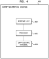
- the cryptographic device 600 comprises an interface unit 602, cryptographic hardware 608 and a processor 606.
- the interface unit 602 is configured to receive input data and is configured to output cipher text.
- the cryptographic hardware 608 comprises a logic core, such as core 102 or 104, which comprises a plurality of cryptographic logic units (e.g., two or more of logic unit A, logic unit B, logic unit C, etc.), as described hereinabove.
- the interface unit 602 and the cryptographic hardware are coupled to the processor 606.
- the processor 606 is a microprocessor or microcontroller that is configured to execute program logic instructions for carrying out various operations and tasks described herein.
- processor 606 may cause hardware 608 to perform the enhanced cryptography techniques described herein.
- the functions of processor 606 may be implemented by logic encoded in one or more tangible computer readable media (e.g., embedded logic such as an application specific integrated circuit, digital signal processor instructions, software that is executed by a processor, etc.)
- a method comprising: in an electronic device configured to perform cryptography, receiving input data; sending the input data to a first logic unit; sending random data to a second logic unit, wherein the second logic unit is identical to the first logic unit; using the first logic unit, performing first cryptographic operations on the input data; using the second logic unit, performing first processing operations on the random data, wherein the first processing operations occur in synchrony with the first cryptographic operations; sending output data generated by the first logic unit to the second logic unit; sending output data generated by the second logic unit to the first logic unit; using the first logic unit, performing second processing operations on the output data generated by the second logic unit; and using the second logic unit, performing second cryptographic operations on the output data generated by the first logic unit, wherein the second cryptographic operations occur in synchrony with the second processing operations.
- These operations may be repeated iteratively as many times as required to give the desired cryptographic result.
- an apparatus comprising: a first logic unit comprising a first flip-flop array and a first combinational logic; and a second logic unit configured identically to the first logic unit and comprising a second flip-flop array and a second combinational logic, wherein an output node of the first logic unit is configured to operate as an input node of the second logic unit such that output from the first logic unit is input to the second logic unit and wherein an output node of the second logic unit is configured to operate as an input node of first logic unit such that output of the second logic unit is input to the first logic unit.
- an apparatus comprising: a first logic unit comprising a first flip-flop array and a first combinational logic; a second logic unit configured identically to the first logic unit and comprising a second flip-flop array and a second combinational logic; and a third logic unit configured identically to the first logic unit and comprising a third flip-flop array and a third combination logic, wherein: an output node of the first logic unit is configured to operate as an input node of the second logic unit such that output from the first logic unit is input to the second logic unit; an output node of the second logic unit is configured to operate as an input node of the third logic unit such that the output from the second logic unit is input to the third logic unit; and an output node of the third logic unit is configured to operate as an input node of the first logic unit such that the output from the third logic unit is input to the first logic unit.
Landscapes
- Engineering & Computer Science (AREA)
- Computer Security & Cryptography (AREA)
- Computer Networks & Wireless Communication (AREA)
- Signal Processing (AREA)
- Storage Device Security (AREA)
- Theoretical Computer Science (AREA)
- Physics & Mathematics (AREA)
- General Engineering & Computer Science (AREA)
- General Physics & Mathematics (AREA)
Claims (14)
- Dispositif cryptographique (600), comprenant :une entrée de dispositif (308), couplée pour recevoir une première valeur d'entrée (308) ;une sortie de dispositif (312) ; etun cœur logique, couplé à l'entrée de dispositif (308) afin de recevoir et de traiter la première valeur d'entrée au moyen d'une valeur secrète stockée dans le cœur logique afin de fournir une valeur de sortie au niveau de la sortie de dispositif (312), le cœur logique comprenant :un générateur d'entrée (310), configuré pour fournir une seconde valeur d'entrée qui n'est pas corrélée à la première valeur d'entrée ; etune pluralité d'unités logiques, comprenant au moins :une première unité logique (302a), comprenant une première entrée logique (304a) qui est couplée pour recevoir, à un cycle initial du dispositif cryptographique, la première valeur d'entrée en provenance de l'entrée de dispositif (308) et pour recevoir, à des cycles postérieurs du dispositif cryptographique, des premières valeurs intermédiaires générées par une autre des unités logiques ; et une première logique de traitement configurée pour opérer sur des premières valeurs fournies par la première entrée logique (304a) au moyen de la valeur secrète, de manière à générer des deuxièmes valeurs intermédiaires ; etune deuxième unité logique (302b), comprenant une deuxième entrée logique (304b) qui est couplée pour recevoir, au cycle initial du dispositif cryptographique, la seconde valeur d'entrée en provenance du générateur d'entrée (310) et pour recevoir, à des cycles postérieurs du dispositif cryptographique, les deuxièmes valeurs intermédiaires ; et une deuxième logique de traitement identique à la première logique de traitement et configurée pour opérer, en synchronisme avec la première logique de traitement, sur des deuxièmes valeurs de données fournies par la deuxième entrée logique (304b), de manière à générer d'autres valeurs intermédiaires destinées à être entrées dans une autre des unités logiques.
- Dispositif cryptographique (600) selon la revendication 1, dans lequel le générateur d'entrée (310) comprend un générateur de données aléatoires, de sorte que la seconde valeur d'entrée soit une valeur aléatoire.
- Dispositif cryptographique (600) selon la revendication 1 ou 2, dans lequel la première entrée logique (304a) est couplée pour recevoir, aux cycles postérieurs du dispositif, les autres valeurs intermédiaires générées par la deuxième logique de traitement, les premières valeurs intermédiaires comprenant les autres valeurs intermédiaires.
- Dispositif cryptographique (600) selon l'une quelconque des revendications 1 à 3, dans lequel la pluralité des unités logiques comprend une troisième unité logique (302c), comprenant une troisième entrée logique, qui est couplée pour recevoir les autres valeurs intermédiaires générées par la deuxième logique de traitement, et une troisième logique de traitement identique aux première et deuxième logiques de traitement et configurée pour opérer, en synchronisme avec les première et deuxième logiques de traitement, sur des troisièmes valeurs de données fournies par la troisième entrée logique.
- Dispositif cryptographique (600) selon la 4, dans lequel la première entrée logique (304a) est couplée pour recevoir, aux cycles postérieurs du dispositif, des troisièmes valeurs intermédiaires générées par la troisième logique de traitement en vue de leur traitement par la première logique de traitement, les premières valeurs intermédiaires comprenant les troisièmes valeurs intermédiaires.
- Dispositif cryptographique (600) selon l'une quelconque des revendications 1 à 5, dans lequel la deuxième logique de traitement est configurée pour opérer sur les deuxièmes valeurs de données au moyen de la même valeur secrète que la première logique de traitement.
- Dispositif cryptographique (600) selon l'une quelconque des revendications 1 à 5, dans lequel la deuxième logique de traitement est configurée pour opérer sur les deuxièmes valeurs de données au moyen d'une autre valeur secrète, différente de la valeur secrète utilisée par la première logique de traitement.
- Procédé comprenant les étapes consistant à :recevoir, au niveau d'une entrée de dispositif (308) d'un dispositif cryptographique comprenant une pluralité d'unités logiques, une première valeur d'entrée ;fournir, dans le dispositif, une seconde valeur d'entrée qui n'est pas corrigée avec la première valeur d'entrée ; ettraiter les première et seconde valeurs d'entrée dans un noyau logique comprenant une pluralité d'unités logiques, au moyen d'une valeur secrète stockée dans le dispositif cryptographique, de manière à fournir une valeur de sortie au niveau d'une sortie de dispositif (312) du dispositif,la pluralité des unités logiques comprenant au moins :une première unité logique, comprenant une première entrée logique (304a) qui reçoit, à un cycle initial du dispositif cryptographique, la première valeur d'entrée en provenance de l'entrée de dispositif (308) et qui reçoit, à des cycles postérieurs du dispositif cryptographique, des premières valeurs intermédiaires générées par une autre des unités logiques ; et une première logique de traitement opérant sur des premières valeurs fournies par la première entrée logique (304a) au moyen de la valeur secrète pour générer une deuxième valeur intermédiaire ; etune deuxième unité logique, comprenant une deuxième entrée logique (304b) qui reçoit, au cycle initial du dispositif cryptographique, la seconde valeur d'entrée et qui reçoit, à des cycles postérieurs du dispositif cryptographique, les deuxièmes valeurs intermédiaires ; et une deuxième logique de traitement identique à la première logique de traitement et opérant, en synchronisme avec la première logique de traitement sur des deuxièmes valeurs de données fournies par la deuxième entrée logique (304b) pour générer d'autres valeurs intermédiaires destinées à être entrées dans une autre des unités logiques.
- Procédé selon la revendication 8, dans lequel la fourniture de la seconde valeur d'entrée consiste à générer une valeur aléatoire.
- Procédé selon la revendication 8 ou 9, dans lequel le traitement des première et seconde valeurs d'entrée consiste à recevoir, au niveau de la première entrée logique (304a), aux cycles postérieurs du dispositif cryptographique, les autres valeurs intermédiaires générées par la deuxième logique de traitement, les premières valeurs intermédiaires comprenant les autres valeurs intermédiaires.
- Procédé selon l'une quelconque des revendications 8 à 10, dans lequel la pluralité des unités logiques comprend une troisième unité logique (302c), comprenant une troisième entrée logique, qui reçoit les autres valeurs intermédiaires générées par la deuxième logique de traitement, et une troisième logique de traitement identique aux première et deuxième logiques de traitement et opérant, en synchronisme avec les première et deuxième logiques de traitement, sur des troisièmes valeurs de données fournies par la troisième entrée logique.
- Procédé selon la revendication 11, dans lequel le traitement des première et seconde valeurs d'entrée consiste à recevoir, au niveau de la première entrée logique (304a), aux cycles postérieurs du dispositif, des troisièmes valeurs intermédiaires générées par la troisième logique de traitement en vue de leur traitement par la première logique de traitement, les premières valeurs intermédiaires comprenant les troisièmes valeurs intermédiaires.
- Procédé selon l'une quelconque des revendications 8 à 12, dans lequel le traitement des première et seconde valeurs d'entrée consiste à opérer sur les deuxièmes valeurs de données dans la deuxième logique de traitement au moyen de la même valeur secrète que la première logique de traitement.
- Procédé selon l'une quelconque des revendications 8 à 12, dans lequel le traitement des première et seconde valeurs d'entrée consiste à opérer sur les deuxièmes valeurs de données dans la deuxième logique de traitement au moyen d'une autre valeur secrète, différente de la valeur secrète utilisée par la première logique de traitement.
Applications Claiming Priority (3)
| Application Number | Priority Date | Filing Date | Title |
|---|---|---|---|
| IL23316414 | 2014-06-16 | ||
| US14/607,137 US9871651B2 (en) | 2014-06-16 | 2015-01-28 | Differential power analysis countermeasures |
| PCT/IB2015/054508 WO2015193789A1 (fr) | 2014-06-16 | 2015-06-15 | Contre-mesures d'analyse de puissance différentielle |
Publications (3)
| Publication Number | Publication Date |
|---|---|
| EP3143720A1 EP3143720A1 (fr) | 2017-03-22 |
| EP3143720A4 EP3143720A4 (fr) | 2018-02-14 |
| EP3143720B1 true EP3143720B1 (fr) | 2020-08-05 |
Family
ID=54837093
Family Applications (1)
| Application Number | Title | Priority Date | Filing Date |
|---|---|---|---|
| EP15809894.7A Active EP3143720B1 (fr) | 2014-06-16 | 2015-06-15 | Contre-mesures d'analyse de puissance différentielle |
Country Status (4)
| Country | Link |
|---|---|
| US (1) | US9871651B2 (fr) |
| EP (1) | EP3143720B1 (fr) |
| CN (1) | CN106664204B (fr) |
| WO (1) | WO2015193789A1 (fr) |
Families Citing this family (15)
| Publication number | Priority date | Publication date | Assignee | Title |
|---|---|---|---|---|
| US10530566B2 (en) * | 2015-04-23 | 2020-01-07 | Cryptography Research, Inc. | Configuring a device based on a DPA countermeasure |
| US20170180131A1 (en) * | 2015-12-16 | 2017-06-22 | Intel Corporation | Secure unlock to access debug hardware |
| US10200192B2 (en) * | 2017-04-19 | 2019-02-05 | Seagate Technology Llc | Secure execution environment clock frequency hopping |
| US10459477B2 (en) | 2017-04-19 | 2019-10-29 | Seagate Technology Llc | Computing system with power variation attack countermeasures |
| US10270586B2 (en) | 2017-04-25 | 2019-04-23 | Seagate Technology Llc | Random time generated interrupts in a cryptographic hardware pipeline circuit |
| US10511433B2 (en) | 2017-05-03 | 2019-12-17 | Seagate Technology Llc | Timing attack protection in a cryptographic processing system |
| US10771236B2 (en) | 2017-05-03 | 2020-09-08 | Seagate Technology Llc | Defending against a side-channel information attack in a data storage device |
| US11308239B2 (en) | 2018-03-30 | 2022-04-19 | Seagate Technology Llc | Jitter attack protection circuit |
| US10979054B1 (en) * | 2020-01-14 | 2021-04-13 | Nuvotonn Technology Corporation | Coupling of combinational logic circuits for protection against side-channel attacks |
| US11741227B2 (en) | 2021-06-22 | 2023-08-29 | Intel Corporation | Platform security mechanism |
| US12015622B2 (en) * | 2021-03-01 | 2024-06-18 | Old Dominion University | Privacy-preserving online botnet classification system utilizing power footprint of IoT connected devices |
| US12174955B2 (en) * | 2021-06-22 | 2024-12-24 | Intel Corporation | Integrated circuit side-channel mitigation mechanism |
| US11995191B2 (en) | 2021-06-25 | 2024-05-28 | FortifyIQ, Inc. | Side-channel attack on HMAC-SHA-2 and associated testing |
| WO2022272289A1 (fr) * | 2021-06-25 | 2022-12-29 | FortifyIQ, Inc. | Noyau semi-conducteur de propriété intellectuelle et procédés d'amélioration de performances de processeur de données et d'attaque de canal latéral sur hmac-sha-2 |
| WO2023164567A2 (fr) | 2022-02-24 | 2023-08-31 | FortifyIQ, Inc. | Analyse de puissance différentielle basée sur un report et son application à un test de vulnérabilité de sha-2 et de hmac-sha-2 à une attaque de canal latéral |
Family Cites Families (13)
| Publication number | Priority date | Publication date | Assignee | Title |
|---|---|---|---|---|
| EP1088295B1 (fr) | 1998-06-03 | 2007-08-15 | Cryptography Research Inc. | Procede de calcul cryptographique equilibre et dispositif de minimisation de fuites dans les cartes a puce et autres cryptosystemes |
| DE10000503A1 (de) * | 2000-01-08 | 2001-07-12 | Philips Corp Intellectual Pty | Datenverarbeitungseinrichtung und Verfahren zu dessen Betrieb |
| US6876746B2 (en) * | 2001-05-15 | 2005-04-05 | Sony Corporation | Encryption/decryption engine for multiple isochronous data streams |
| JP4596686B2 (ja) | 2001-06-13 | 2010-12-08 | 富士通株式会社 | Dpaに対して安全な暗号化 |
| US7899190B2 (en) * | 2004-04-16 | 2011-03-01 | Research In Motion Limited | Security countermeasures for power analysis attacks |
| EP1840732A1 (fr) * | 2006-03-31 | 2007-10-03 | Axalto SA | Protection contre les attaques latérales de la chaîne |
| US8386800B2 (en) | 2009-12-04 | 2013-02-26 | Cryptography Research, Inc. | Verifiable, leak-resistant encryption and decryption |
| JP2011169977A (ja) * | 2010-02-16 | 2011-09-01 | Renesas Electronics Corp | 暗号処理装置 |
| US8522052B1 (en) | 2010-04-07 | 2013-08-27 | Xilinx, Inc. | Method and integrated circuit for secure encryption and decryption |
| CN102752103B (zh) * | 2012-07-26 | 2015-01-28 | 上海爱信诺航芯电子科技有限公司 | 一种抗des功耗攻击的增强型mask掩码方法 |
| US8892903B1 (en) * | 2012-12-06 | 2014-11-18 | Xilinx, Inc. | Detection of power analysis attacks |
| CN103905462B (zh) * | 2014-04-16 | 2017-05-17 | 深圳国微技术有限公司 | 可抵御差分功耗分析攻击的加密处理装置及方法 |
| US9531384B1 (en) * | 2014-12-01 | 2016-12-27 | University Of South Florida | Adiabatic dynamic differential logic for differential power analysis resistant secure integrated circuits |
-
2015
- 2015-01-28 US US14/607,137 patent/US9871651B2/en active Active
- 2015-06-15 CN CN201580032295.3A patent/CN106664204B/zh active Active
- 2015-06-15 EP EP15809894.7A patent/EP3143720B1/fr active Active
- 2015-06-15 WO PCT/IB2015/054508 patent/WO2015193789A1/fr not_active Ceased
Non-Patent Citations (1)
| Title |
|---|
| None * |
Also Published As
| Publication number | Publication date |
|---|---|
| US9871651B2 (en) | 2018-01-16 |
| CN106664204A (zh) | 2017-05-10 |
| US20150365228A1 (en) | 2015-12-17 |
| WO2015193789A1 (fr) | 2015-12-23 |
| EP3143720A1 (fr) | 2017-03-22 |
| CN106664204B (zh) | 2020-04-07 |
| EP3143720A4 (fr) | 2018-02-14 |
Similar Documents
| Publication | Publication Date | Title |
|---|---|---|
| EP3143720B1 (fr) | Contre-mesures d'analyse de puissance différentielle | |
| KR101680918B1 (ko) | 특히 고차의 관측 공격에 대해 보호되는 암호화 회로 | |
| Barenghi et al. | Fault injection attacks on cryptographic devices: Theory, practice, and countermeasures | |
| KR102628466B1 (ko) | 메시지 부호화 및 복호화를 위한 블록 암호화 방법 및 이 방법을 구현하기 위한 암호화 장치 | |
| US10644873B2 (en) | Method for protecting substitution operation against side-channel analysis | |
| Backlund et al. | Secret key recovery attack on masked and shuffled implementations of crystals-kyber and saber | |
| CN112906070B (zh) | 具有块密码侧信道攻击减轻的集成电路和IoT设备及相关方法 | |
| Bellizia et al. | Secure double rate registers as an RTL countermeasure against power analysis attacks | |
| Jati et al. | Threshold Implementations of $\mathtt {GIFT} $: A Trade-Off Analysis | |
| US11431491B2 (en) | Protection of the execution of cipher algorithms | |
| Tsoutsos et al. | Advanced techniques for designing stealthy hardware trojans | |
| Kumari et al. | Lightweight encryption with data and device integrity using NLFSR and PUF for the Internet of Medical Things | |
| Kasper et al. | Side channels as building blocks | |
| Dhanuskodi et al. | Efficient register renaming architectures for 8-bit AES datapath at 0.55 pJ/bit in 16-nm FinFET | |
| CN103636159B (zh) | 用于产生随机的输出位序列的方法 | |
| EP4307155A1 (fr) | Procédé et circuit pour protéger un dispositif électronique contre une attaque par canal latéral | |
| CN101488846A (zh) | 密码保护方法和系统 | |
| Mischke et al. | Fault sensitivity analysis meets zero-value attack | |
| Wang et al. | Mind the Faulty Keccak: A Practical Fault Injection Attack Scheme Apply to All Phases of ML-KEM and ML-DSA | |
| Mazumdar et al. | A compact implementation of Salsa20 and its power analysis vulnerabilities | |
| Lee et al. | Systematization of shuffling countermeasures: With an application to crystals-dilithium | |
| Korkikian | Side-channel and fault analysis in the presence of countermeasures: tools, theory, and practice | |
| Chhabra et al. | Towards the enhancement of AES IP security using hardware obfuscation technique: A practical approach for secure data transmission in IoT | |
| Zadeh et al. | Application of simple power analysis to stream ciphers constructed using feedback shift registers | |
| Repka et al. | Improving CPA attack against DSA and ECDSA |
Legal Events
| Date | Code | Title | Description |
|---|---|---|---|
| STAA | Information on the status of an ep patent application or granted ep patent |
Free format text: STATUS: THE INTERNATIONAL PUBLICATION HAS BEEN MADE |
|
| PUAI | Public reference made under article 153(3) epc to a published international application that has entered the european phase |
Free format text: ORIGINAL CODE: 0009012 |
|
| STAA | Information on the status of an ep patent application or granted ep patent |
Free format text: STATUS: REQUEST FOR EXAMINATION WAS MADE |
|
| 17P | Request for examination filed |
Effective date: 20161212 |
|
| AK | Designated contracting states |
Kind code of ref document: A1 Designated state(s): AL AT BE BG CH CY CZ DE DK EE ES FI FR GB GR HR HU IE IS IT LI LT LU LV MC MK MT NL NO PL PT RO RS SE SI SK SM TR |
|
| AX | Request for extension of the european patent |
Extension state: BA ME |
|
| DAV | Request for validation of the european patent (deleted) | ||
| DAX | Request for extension of the european patent (deleted) | ||
| REG | Reference to a national code |
Ref country code: DE Ref legal event code: R079 Ref document number: 602015057054 Country of ref document: DE Free format text: PREVIOUS MAIN CLASS: H04L0009280000 Ipc: H04L0009000000 |
|
| A4 | Supplementary search report drawn up and despatched |
Effective date: 20180116 |
|
| RIC1 | Information provided on ipc code assigned before grant |
Ipc: H04L 9/00 20060101AFI20180110BHEP |
|
| GRAP | Despatch of communication of intention to grant a patent |
Free format text: ORIGINAL CODE: EPIDOSNIGR1 |
|
| STAA | Information on the status of an ep patent application or granted ep patent |
Free format text: STATUS: GRANT OF PATENT IS INTENDED |
|
| INTG | Intention to grant announced |
Effective date: 20200130 |
|
| GRAS | Grant fee paid |
Free format text: ORIGINAL CODE: EPIDOSNIGR3 |
|
| GRAA | (expected) grant |
Free format text: ORIGINAL CODE: 0009210 |
|
| STAA | Information on the status of an ep patent application or granted ep patent |
Free format text: STATUS: THE PATENT HAS BEEN GRANTED |
|
| AK | Designated contracting states |
Kind code of ref document: B1 Designated state(s): AL AT BE BG CH CY CZ DE DK EE ES FI FR GB GR HR HU IE IS IT LI LT LU LV MC MK MT NL NO PL PT RO RS SE SI SK SM TR |
|
| REG | Reference to a national code |
Ref country code: GB Ref legal event code: FG4D |
|
| REG | Reference to a national code |
Ref country code: CH Ref legal event code: EP |
|
| REG | Reference to a national code |
Ref country code: AT Ref legal event code: REF Ref document number: 1300246 Country of ref document: AT Kind code of ref document: T Effective date: 20200815 |
|
| REG | Reference to a national code |
Ref country code: DE Ref legal event code: R096 Ref document number: 602015057054 Country of ref document: DE |
|
| REG | Reference to a national code |
Ref country code: IE Ref legal event code: FG4D |
|
| REG | Reference to a national code |
Ref country code: LT Ref legal event code: MG4D |
|
| REG | Reference to a national code |
Ref country code: NL Ref legal event code: MP Effective date: 20200805 |
|
| REG | Reference to a national code |
Ref country code: AT Ref legal event code: MK05 Ref document number: 1300246 Country of ref document: AT Kind code of ref document: T Effective date: 20200805 |
|
| PG25 | Lapsed in a contracting state [announced via postgrant information from national office to epo] |
Ref country code: FI Free format text: LAPSE BECAUSE OF FAILURE TO SUBMIT A TRANSLATION OF THE DESCRIPTION OR TO PAY THE FEE WITHIN THE PRESCRIBED TIME-LIMIT Effective date: 20200805 Ref country code: NO Free format text: LAPSE BECAUSE OF FAILURE TO SUBMIT A TRANSLATION OF THE DESCRIPTION OR TO PAY THE FEE WITHIN THE PRESCRIBED TIME-LIMIT Effective date: 20201105 Ref country code: GR Free format text: LAPSE BECAUSE OF FAILURE TO SUBMIT A TRANSLATION OF THE DESCRIPTION OR TO PAY THE FEE WITHIN THE PRESCRIBED TIME-LIMIT Effective date: 20201106 Ref country code: HR Free format text: LAPSE BECAUSE OF FAILURE TO SUBMIT A TRANSLATION OF THE DESCRIPTION OR TO PAY THE FEE WITHIN THE PRESCRIBED TIME-LIMIT Effective date: 20200805 Ref country code: AT Free format text: LAPSE BECAUSE OF FAILURE TO SUBMIT A TRANSLATION OF THE DESCRIPTION OR TO PAY THE FEE WITHIN THE PRESCRIBED TIME-LIMIT Effective date: 20200805 Ref country code: BG Free format text: LAPSE BECAUSE OF FAILURE TO SUBMIT A TRANSLATION OF THE DESCRIPTION OR TO PAY THE FEE WITHIN THE PRESCRIBED TIME-LIMIT Effective date: 20201105 Ref country code: SE Free format text: LAPSE BECAUSE OF FAILURE TO SUBMIT A TRANSLATION OF THE DESCRIPTION OR TO PAY THE FEE WITHIN THE PRESCRIBED TIME-LIMIT Effective date: 20200805 Ref country code: PT Free format text: LAPSE BECAUSE OF FAILURE TO SUBMIT A TRANSLATION OF THE DESCRIPTION OR TO PAY THE FEE WITHIN THE PRESCRIBED TIME-LIMIT Effective date: 20201207 Ref country code: ES Free format text: LAPSE BECAUSE OF FAILURE TO SUBMIT A TRANSLATION OF THE DESCRIPTION OR TO PAY THE FEE WITHIN THE PRESCRIBED TIME-LIMIT Effective date: 20200805 Ref country code: LT Free format text: LAPSE BECAUSE OF FAILURE TO SUBMIT A TRANSLATION OF THE DESCRIPTION OR TO PAY THE FEE WITHIN THE PRESCRIBED TIME-LIMIT Effective date: 20200805 |
|
| PG25 | Lapsed in a contracting state [announced via postgrant information from national office to epo] |
Ref country code: PL Free format text: LAPSE BECAUSE OF FAILURE TO SUBMIT A TRANSLATION OF THE DESCRIPTION OR TO PAY THE FEE WITHIN THE PRESCRIBED TIME-LIMIT Effective date: 20200805 Ref country code: LV Free format text: LAPSE BECAUSE OF FAILURE TO SUBMIT A TRANSLATION OF THE DESCRIPTION OR TO PAY THE FEE WITHIN THE PRESCRIBED TIME-LIMIT Effective date: 20200805 Ref country code: RS Free format text: LAPSE BECAUSE OF FAILURE TO SUBMIT A TRANSLATION OF THE DESCRIPTION OR TO PAY THE FEE WITHIN THE PRESCRIBED TIME-LIMIT Effective date: 20200805 Ref country code: NL Free format text: LAPSE BECAUSE OF FAILURE TO SUBMIT A TRANSLATION OF THE DESCRIPTION OR TO PAY THE FEE WITHIN THE PRESCRIBED TIME-LIMIT Effective date: 20200805 Ref country code: IS Free format text: LAPSE BECAUSE OF FAILURE TO SUBMIT A TRANSLATION OF THE DESCRIPTION OR TO PAY THE FEE WITHIN THE PRESCRIBED TIME-LIMIT Effective date: 20201205 |
|
| PG25 | Lapsed in a contracting state [announced via postgrant information from national office to epo] |
Ref country code: CZ Free format text: LAPSE BECAUSE OF FAILURE TO SUBMIT A TRANSLATION OF THE DESCRIPTION OR TO PAY THE FEE WITHIN THE PRESCRIBED TIME-LIMIT Effective date: 20200805 Ref country code: DK Free format text: LAPSE BECAUSE OF FAILURE TO SUBMIT A TRANSLATION OF THE DESCRIPTION OR TO PAY THE FEE WITHIN THE PRESCRIBED TIME-LIMIT Effective date: 20200805 Ref country code: SM Free format text: LAPSE BECAUSE OF FAILURE TO SUBMIT A TRANSLATION OF THE DESCRIPTION OR TO PAY THE FEE WITHIN THE PRESCRIBED TIME-LIMIT Effective date: 20200805 Ref country code: RO Free format text: LAPSE BECAUSE OF FAILURE TO SUBMIT A TRANSLATION OF THE DESCRIPTION OR TO PAY THE FEE WITHIN THE PRESCRIBED TIME-LIMIT Effective date: 20200805 Ref country code: EE Free format text: LAPSE BECAUSE OF FAILURE TO SUBMIT A TRANSLATION OF THE DESCRIPTION OR TO PAY THE FEE WITHIN THE PRESCRIBED TIME-LIMIT Effective date: 20200805 |
|
| REG | Reference to a national code |
Ref country code: DE Ref legal event code: R097 Ref document number: 602015057054 Country of ref document: DE |
|
| PG25 | Lapsed in a contracting state [announced via postgrant information from national office to epo] |
Ref country code: AL Free format text: LAPSE BECAUSE OF FAILURE TO SUBMIT A TRANSLATION OF THE DESCRIPTION OR TO PAY THE FEE WITHIN THE PRESCRIBED TIME-LIMIT Effective date: 20200805 |
|
| PLBE | No opposition filed within time limit |
Free format text: ORIGINAL CODE: 0009261 |
|
| STAA | Information on the status of an ep patent application or granted ep patent |
Free format text: STATUS: NO OPPOSITION FILED WITHIN TIME LIMIT |
|
| PG25 | Lapsed in a contracting state [announced via postgrant information from national office to epo] |
Ref country code: SK Free format text: LAPSE BECAUSE OF FAILURE TO SUBMIT A TRANSLATION OF THE DESCRIPTION OR TO PAY THE FEE WITHIN THE PRESCRIBED TIME-LIMIT Effective date: 20200805 |
|
| 26N | No opposition filed |
Effective date: 20210507 |
|
| PG25 | Lapsed in a contracting state [announced via postgrant information from national office to epo] |
Ref country code: IT Free format text: LAPSE BECAUSE OF FAILURE TO SUBMIT A TRANSLATION OF THE DESCRIPTION OR TO PAY THE FEE WITHIN THE PRESCRIBED TIME-LIMIT Effective date: 20200805 |
|
| PG25 | Lapsed in a contracting state [announced via postgrant information from national office to epo] |
Ref country code: SI Free format text: LAPSE BECAUSE OF FAILURE TO SUBMIT A TRANSLATION OF THE DESCRIPTION OR TO PAY THE FEE WITHIN THE PRESCRIBED TIME-LIMIT Effective date: 20200805 |
|
| REG | Reference to a national code |
Ref country code: DE Ref legal event code: R119 Ref document number: 602015057054 Country of ref document: DE |
|
| PG25 | Lapsed in a contracting state [announced via postgrant information from national office to epo] |
Ref country code: MC Free format text: LAPSE BECAUSE OF FAILURE TO SUBMIT A TRANSLATION OF THE DESCRIPTION OR TO PAY THE FEE WITHIN THE PRESCRIBED TIME-LIMIT Effective date: 20200805 |
|
| REG | Reference to a national code |
Ref country code: CH Ref legal event code: PL |
|
| REG | Reference to a national code |
Ref country code: BE Ref legal event code: MM Effective date: 20210630 |
|
| PG25 | Lapsed in a contracting state [announced via postgrant information from national office to epo] |
Ref country code: LU Free format text: LAPSE BECAUSE OF NON-PAYMENT OF DUE FEES Effective date: 20210615 |
|
| PG25 | Lapsed in a contracting state [announced via postgrant information from national office to epo] |
Ref country code: LI Free format text: LAPSE BECAUSE OF NON-PAYMENT OF DUE FEES Effective date: 20210630 Ref country code: IE Free format text: LAPSE BECAUSE OF NON-PAYMENT OF DUE FEES Effective date: 20210615 Ref country code: DE Free format text: LAPSE BECAUSE OF NON-PAYMENT OF DUE FEES Effective date: 20220101 Ref country code: CH Free format text: LAPSE BECAUSE OF NON-PAYMENT OF DUE FEES Effective date: 20210630 |
|
| PG25 | Lapsed in a contracting state [announced via postgrant information from national office to epo] |
Ref country code: FR Free format text: LAPSE BECAUSE OF NON-PAYMENT OF DUE FEES Effective date: 20210630 |
|
| PG25 | Lapsed in a contracting state [announced via postgrant information from national office to epo] |
Ref country code: BE Free format text: LAPSE BECAUSE OF NON-PAYMENT OF DUE FEES Effective date: 20210630 |
|
| PG25 | Lapsed in a contracting state [announced via postgrant information from national office to epo] |
Ref country code: HU Free format text: LAPSE BECAUSE OF FAILURE TO SUBMIT A TRANSLATION OF THE DESCRIPTION OR TO PAY THE FEE WITHIN THE PRESCRIBED TIME-LIMIT; INVALID AB INITIO Effective date: 20150615 |
|
| PG25 | Lapsed in a contracting state [announced via postgrant information from national office to epo] |
Ref country code: CY Free format text: LAPSE BECAUSE OF FAILURE TO SUBMIT A TRANSLATION OF THE DESCRIPTION OR TO PAY THE FEE WITHIN THE PRESCRIBED TIME-LIMIT Effective date: 20200805 |
|
| P01 | Opt-out of the competence of the unified patent court (upc) registered |
Effective date: 20230525 |
|
| PG25 | Lapsed in a contracting state [announced via postgrant information from national office to epo] |
Ref country code: MK Free format text: LAPSE BECAUSE OF FAILURE TO SUBMIT A TRANSLATION OF THE DESCRIPTION OR TO PAY THE FEE WITHIN THE PRESCRIBED TIME-LIMIT Effective date: 20200805 |
|
| PG25 | Lapsed in a contracting state [announced via postgrant information from national office to epo] |
Ref country code: TR Free format text: LAPSE BECAUSE OF FAILURE TO SUBMIT A TRANSLATION OF THE DESCRIPTION OR TO PAY THE FEE WITHIN THE PRESCRIBED TIME-LIMIT Effective date: 20200805 |
|
| PG25 | Lapsed in a contracting state [announced via postgrant information from national office to epo] |
Ref country code: MT Free format text: LAPSE BECAUSE OF FAILURE TO SUBMIT A TRANSLATION OF THE DESCRIPTION OR TO PAY THE FEE WITHIN THE PRESCRIBED TIME-LIMIT Effective date: 20200805 |
|
| PGFP | Annual fee paid to national office [announced via postgrant information from national office to epo] |
Ref country code: GB Payment date: 20250604 Year of fee payment: 11 |