EP3144581A1 - Module de rétroéclairage et dispositif d'affichage - Google Patents
Module de rétroéclairage et dispositif d'affichage Download PDFInfo
- Publication number
- EP3144581A1 EP3144581A1 EP14870642.7A EP14870642A EP3144581A1 EP 3144581 A1 EP3144581 A1 EP 3144581A1 EP 14870642 A EP14870642 A EP 14870642A EP 3144581 A1 EP3144581 A1 EP 3144581A1
- Authority
- EP
- European Patent Office
- Prior art keywords
- light source
- light
- source elements
- backlight module
- display device
- Prior art date
- Legal status (The legal status is an assumption and is not a legal conclusion. Google has not performed a legal analysis and makes no representation as to the accuracy of the status listed.)
- Granted
Links
Images
Classifications
-
- F—MECHANICAL ENGINEERING; LIGHTING; HEATING; WEAPONS; BLASTING
- F21—LIGHTING
- F21V—FUNCTIONAL FEATURES OR DETAILS OF LIGHTING DEVICES OR SYSTEMS THEREOF; STRUCTURAL COMBINATIONS OF LIGHTING DEVICES WITH OTHER ARTICLES, NOT OTHERWISE PROVIDED FOR
- F21V5/00—Refractors for light sources
- F21V5/02—Refractors for light sources of prismatic shape
-
- F—MECHANICAL ENGINEERING; LIGHTING; HEATING; WEAPONS; BLASTING
- F21—LIGHTING
- F21V—FUNCTIONAL FEATURES OR DETAILS OF LIGHTING DEVICES OR SYSTEMS THEREOF; STRUCTURAL COMBINATIONS OF LIGHTING DEVICES WITH OTHER ARTICLES, NOT OTHERWISE PROVIDED FOR
- F21V5/00—Refractors for light sources
- F21V5/04—Refractors for light sources of lens shape
-
- F—MECHANICAL ENGINEERING; LIGHTING; HEATING; WEAPONS; BLASTING
- F21—LIGHTING
- F21V—FUNCTIONAL FEATURES OR DETAILS OF LIGHTING DEVICES OR SYSTEMS THEREOF; STRUCTURAL COMBINATIONS OF LIGHTING DEVICES WITH OTHER ARTICLES, NOT OTHERWISE PROVIDED FOR
- F21V7/00—Reflectors for light sources
- F21V7/0025—Combination of two or more reflectors for a single light source
- F21V7/0033—Combination of two or more reflectors for a single light source with successive reflections from one reflector to the next or following
-
- F—MECHANICAL ENGINEERING; LIGHTING; HEATING; WEAPONS; BLASTING
- F21—LIGHTING
- F21V—FUNCTIONAL FEATURES OR DETAILS OF LIGHTING DEVICES OR SYSTEMS THEREOF; STRUCTURAL COMBINATIONS OF LIGHTING DEVICES WITH OTHER ARTICLES, NOT OTHERWISE PROVIDED FOR
- F21V7/00—Reflectors for light sources
- F21V7/04—Optical design
- F21V7/05—Optical design plane
-
- G—PHYSICS
- G02—OPTICS
- G02F—OPTICAL DEVICES OR ARRANGEMENTS FOR THE CONTROL OF LIGHT BY MODIFICATION OF THE OPTICAL PROPERTIES OF THE MEDIA OF THE ELEMENTS INVOLVED THEREIN; NON-LINEAR OPTICS; FREQUENCY-CHANGING OF LIGHT; OPTICAL LOGIC ELEMENTS; OPTICAL ANALOGUE/DIGITAL CONVERTERS
- G02F1/00—Devices or arrangements for the control of the intensity, colour, phase, polarisation or direction of light arriving from an independent light source, e.g. switching, gating or modulating; Non-linear optics
- G02F1/01—Devices or arrangements for the control of the intensity, colour, phase, polarisation or direction of light arriving from an independent light source, e.g. switching, gating or modulating; Non-linear optics for the control of the intensity, phase, polarisation or colour
- G02F1/13—Devices or arrangements for the control of the intensity, colour, phase, polarisation or direction of light arriving from an independent light source, e.g. switching, gating or modulating; Non-linear optics for the control of the intensity, phase, polarisation or colour based on liquid crystals, e.g. single liquid crystal display cells
- G02F1/133—Constructional arrangements; Operation of liquid crystal cells; Circuit arrangements
- G02F1/1333—Constructional arrangements; Manufacturing methods
- G02F1/1335—Structural association of cells with optical devices, e.g. polarisers or reflectors
- G02F1/1336—Illuminating devices
- G02F1/133602—Direct backlight
- G02F1/133603—Direct backlight with LEDs
-
- G—PHYSICS
- G02—OPTICS
- G02F—OPTICAL DEVICES OR ARRANGEMENTS FOR THE CONTROL OF LIGHT BY MODIFICATION OF THE OPTICAL PROPERTIES OF THE MEDIA OF THE ELEMENTS INVOLVED THEREIN; NON-LINEAR OPTICS; FREQUENCY-CHANGING OF LIGHT; OPTICAL LOGIC ELEMENTS; OPTICAL ANALOGUE/DIGITAL CONVERTERS
- G02F1/00—Devices or arrangements for the control of the intensity, colour, phase, polarisation or direction of light arriving from an independent light source, e.g. switching, gating or modulating; Non-linear optics
- G02F1/01—Devices or arrangements for the control of the intensity, colour, phase, polarisation or direction of light arriving from an independent light source, e.g. switching, gating or modulating; Non-linear optics for the control of the intensity, phase, polarisation or colour
- G02F1/13—Devices or arrangements for the control of the intensity, colour, phase, polarisation or direction of light arriving from an independent light source, e.g. switching, gating or modulating; Non-linear optics for the control of the intensity, phase, polarisation or colour based on liquid crystals, e.g. single liquid crystal display cells
- G02F1/133—Constructional arrangements; Operation of liquid crystal cells; Circuit arrangements
- G02F1/1333—Constructional arrangements; Manufacturing methods
- G02F1/1335—Structural association of cells with optical devices, e.g. polarisers or reflectors
- G02F1/1336—Illuminating devices
- G02F1/133602—Direct backlight
- G02F1/133606—Direct backlight including a specially adapted diffusing, scattering or light controlling members
-
- G—PHYSICS
- G02—OPTICS
- G02F—OPTICAL DEVICES OR ARRANGEMENTS FOR THE CONTROL OF LIGHT BY MODIFICATION OF THE OPTICAL PROPERTIES OF THE MEDIA OF THE ELEMENTS INVOLVED THEREIN; NON-LINEAR OPTICS; FREQUENCY-CHANGING OF LIGHT; OPTICAL LOGIC ELEMENTS; OPTICAL ANALOGUE/DIGITAL CONVERTERS
- G02F1/00—Devices or arrangements for the control of the intensity, colour, phase, polarisation or direction of light arriving from an independent light source, e.g. switching, gating or modulating; Non-linear optics
- G02F1/01—Devices or arrangements for the control of the intensity, colour, phase, polarisation or direction of light arriving from an independent light source, e.g. switching, gating or modulating; Non-linear optics for the control of the intensity, phase, polarisation or colour
- G02F1/13—Devices or arrangements for the control of the intensity, colour, phase, polarisation or direction of light arriving from an independent light source, e.g. switching, gating or modulating; Non-linear optics for the control of the intensity, phase, polarisation or colour based on liquid crystals, e.g. single liquid crystal display cells
- G02F1/133—Constructional arrangements; Operation of liquid crystal cells; Circuit arrangements
- G02F1/1333—Constructional arrangements; Manufacturing methods
- G02F1/1335—Structural association of cells with optical devices, e.g. polarisers or reflectors
- G02F1/1336—Illuminating devices
- G02F1/133602—Direct backlight
- G02F1/133606—Direct backlight including a specially adapted diffusing, scattering or light controlling members
- G02F1/133607—Direct backlight including a specially adapted diffusing, scattering or light controlling members the light controlling member including light directing or refracting elements, e.g. prisms or lenses
Definitions
- the present invention relates to the technical field of display, in particular to a backlight module and a display device.
- Backlight sources in the prior art mainly comprises side type backlight source and direct type backlight source; the principle of the backlight source is providing light to a display device, which light is emitted from light source elements set in a backboard of the backlight source.
- Defects of the prior art are that: the brightness adjustment of the display device in the prior art is realized by adjusting the electric current of all the light source elements in the backlight source, the adjustment range is relatively small; moreover, even in a situation that a low brightness is required for the display device, all the light source elements are still in working condition, affecting the service life of the backlight source.
- the present invention provides a backlight module and a display device to improve the adjustment range of the brightness for the display device, improving the display effect of the display device.
- An embodiment of the present invention provides a backlight module; the backlight module comprises:
- light can be provided to the display device by applying one or both of the light source layers, improving the adjustable range of the display brightness for the display device; meanwhile, in a situation that a low brightness is required for the display device, one of the first and the second light source layers can be turned off, reducing the operation time for a part of the light source elements, thereby improving the service life of the light source elements; moreover, when one of the first and the second light source layers fails, another light source layer can still provide light for the display device to ensure the normal operation of the display device, improving the emergency capability of the display device; furthermore, the utilization of light can also be improved by applying the optical components.
- the optical components comprise lenses
- the lenses are arranged one-to-one corresponding to every second light source elements and change propagation path of light from the second light source elements irradiating the first light source elements such that the light is emitted through the intervals.
- the light emitted from the second light source elements can be refracted by the lenses; and propagation path of the light irradiating the first light source elements is changed such that the light irradiates the display panel.
- the lenses are triple prisms or convex lenses. Different lenses can be selected for changing the propagation path of the light.
- the diameter of the convex lens is 1 ⁇ 2 times of the width of the second light source element. In this way it is ensured that the propagation path of the light emitted from the second light source elements can be changed by the convex lenses.
- the diameter of the convex lens is two times of the width of the second light source element. In this way it is further ensured that the propagation path of the light emitted from the second light source elements can be changed by the convex lenses, meanwhile the manufacture of the convex lenses is facilitated.
- the triple prisms are normal triple prisms. In this way it is ensured that the propagation path of the light emitted from the second light source elements can be changed by the normal triple prisms.
- the optical components comprise a first reflective layer arranged on a side of the first light source elements facing the second light source elements, and a second reflective layer arranged between adjacent second light source elements.
- the light irradiating the first light source elements is reflected by the reflective sheet such that the light can irradiate the display panel.
- the width of the second light source element is not greater than the width of the interval between adjacent first light source elements. In this way, it can be avoided that much light is blocked by the first light source elements.
- both the first light source elements and the second light source elements are organic light emitting diode lamp strips. In this way a good light emitting can be ensured.
- the present invention also provides a display device and an electronic equipment comprising the display device; wherein the display device comprises a display panel and above mentioned backlight module, the backlight module is arranged on a light inputting side of the display panel.
- light can be provided to the display device by applying one or both of the light source layers, improving the adjustable range of the display brightness for the display device; meanwhile, in a situation that a low brightness is required for the display device, one of the first and the second light source layers can be turned off, reducing the operation time for a part of the light source elements, thereby improving the service life of the light source elements; moreover, when one of the first and the second light source layers fails, another light source layer can still provide light for the display device to ensure the normal operation of the display device, improving the emergency capability of the display device; furthermore, the utilization of light can also be improved by applying the optical components.
- the present invention provides a backlight module and a display device to improve the adjustment range of the brightness for the display device, improving the display effect of the display device.
- two layers of light source elements are provided, thereby improving the adjustment range of light for the backlight module, and improving the display effect of the display device.
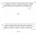
- Fig. 1 shows a structural schematic diagram of a backlight module provided by an embodiment of the present invention
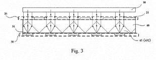
- Fig. 2 shows a structural schematic diagram of a backlight module provided by another embodiment of the present invention.
- An embodiment of the present invention provides a backlight module; the backlight module comprises:
- light can be provided to the display device by the first light source layer 20 or the second light source layer 30 separately.
- a part of the light emitted from the second light source elements 31 of the second light source layer 30 directly irradiates the display panel 10 after passes through the intervals between the first light source elements 21 in the first light source layer 20; the propagation path of another part of the light originally irradiating the first light source elements 21 is changed by the optical components 40, such that the light also irradiates the display panel 10 after passes through the intervals between the first light source elements 21.
- the light originally blocked by the first light source elements 21 can irradiate the display panel 10 after passes through the intervals, thereby improving the utilization of light, providing a brighter image displayed by the display device, and improving the display effect of the display device.
- light can be provided to the display device by separately applying the first light source layer 20, separately applying the second light source layer 30, or simultaneously applying both of the light source layers, improving the adjustable range of the display brightness for the display device; meanwhile, in a situation that a low brightness is required for the display device, one of the first light source layer 20 and the second light source layer 30 can be turned off, reducing the operation time for the turned-off light source elements, thereby improving the service life of the light source elements; moreover, when one of the first light source layer 20 and the second light source layer 30 fails, another light source layer can still provide light for the display device to ensure the normal operation of the display device, improving the emergency capability of the display device; furthermore, the utilization of light can also be improved by applying the optical components.
- the width of the second light source element 31 is not greater than the width of the interval between adjacent first light source elements 21. In this way, it is ensured that more light emitted from the second light source elements 31 can pass through the intervals between the first light source elements 21, improving the situation that the light emitted from the second light source elements 31 is blocked by the first light source elements 21.
- the optical components 40 can be optical components 40 with different structures.
- the structures of the optical components 40 in the display device provided by the embodiments of the present invention are illustrated in detail with Figs. 1-3 .
- Fig. 1 shows a structure of the optical components.
- the optical components 40 can comprise a first reflective layer 42 arranged on a side of the first light source elements 21 facing the second light source elements 31, and a second reflective layer 41 arranged between adjacent second light source elements 31.
- the first reflective layer 42 and the second reflective layer 41 can be metal layers with high reflectance.
- a part of light emitted from the second light source elements 31 irradiates the first light source elements 21.
- the light is reflected by the first reflective layer 42, which is arranged on the first light source elements 21; after being reflected, the light then irradiates the second reflective layer 41 between the second light source elements 31, undergoes reflecting of the second reflective layer 41, and irradiates the display panel 10 through the intervals between the first light source elements 21.
- the light irradiating the first light source elements 21 and originally blocked by the first light source elements 21 can irradiate the display panel 10 after passes through the intervals, thereby improving the utilization of light, providing a brighter image displayed by the display device, and improving the display effect of the display device.
- the first reflective layer 42 and the second reflective layer 41 can be made of metal with high reflectance, improving the reflective effect for light and avoiding the loss of light.
- the optical components 40 comprise lenses 43, the lenses 43 are arranged one-to-one corresponding to every second light source elements 31 and change propagation path of light from the second light source elements 31 irradiating the first light source elements 21 such that the light is emitted through the intervals.
- Different structures can be used as the structure of the lenses 43, as will be illustrated with the following specific embodiment.
- Fig. 2 shows another structure of the optical components.
- the lenses 43 provided in the embodiment are convex lenses 431; each of the convex lenses 431 corresponds to one second light source element 31.
- the light emitted from the second light source elements 31 enters the convex lenses 431.
- the convex lens 431 has a function of converging light: the direction of the light originally irradiating the first light source elements 21 is changed by the refraction of the convex lenses 431, such that the light irradiates the display panel 10 after passes through the intervals between the first light source elements 21, thereby improving the brightness of the display panel 10, and improving the display effect of the display device.
- each of the convex lenses 431 one-to-one corresponds to each of the second light source elements 31; and the second light source element 31 is positioned on a focal plane of the corresponding convex lens 431, such that the light emitted from the second light source element 31 can be converged by the corresponding convex lens 431, ensuring that more light can irradiate the display panel 10.
- the diameter of the convex lens 431 is 1 ⁇ 2 times of the width of the second light source element 31; in this way it is ensured that all of the light emitted from the second light source elements 31 can be converged by the convex lenses 431, improving the utilization of light. More preferably, the diameter of the convex lens 431 is two times of the width of the second light source element 31; in this way the manufacture of the convex lenses 431 and converging of light are facilitated.
- a primary exposure unit can be obtained by way of photolithography on a substrate; a micro rectangular array structure is firstly formed; then the substrate is heated, the hot-melt photoresist forms micro structure of the convex lens 431 due to the effect of surface tension; after heating and curing, the micro lenses structure is then coated with a flat layer.
- the flat layer can be made of organic material, of which the thickness is in millimeter level to ensure the flatness of the surface, facilitating the manufacture of the first light source layer 20.
- the micro structure of the convex lenses 431 can be made of polyester organic material, as long as the refractive index of the polyester organic material (e.g. polycarbonate, with a refractive index of 1.58) is higher than that of the substrate material.
- Fig. 3 shows yet another structure of the optical components.
- the lenses 43 provided in the embodiment are triple prisms 432; each of the triple prisms 432 corresponds to one second light source element 31.
- the light emitted from the second light source elements 31 enters the triple prisms 432.
- the triple prism 432 has a function of converging light: the direction of the light originally irradiating the first light source elements 21 is changed by the refraction of the triple prisms 432, such that the light irradiates the display panel 10 after passes through the intervals between the first light source elements 21, thereby improving the brightness of the display panel 10, and improving the display effect of the display device.
- each of the triple prisms 432 one-to-one corresponds to each of the second light source elements 31; for the positioning of the triple prisms 432, different structures can be applied to refract light to the display panel 10, which light is emitted from the second light source elements 31 and irradiates the first light source elements 21.
- the optical components 40 comprise a substrate material and triple prisms 432 arranged on the substrate material, wherein the refractive index of the triple prisms 432 is higher than that of the substrate material. Referring to Fig. 3 again, the positioning direction shown in Fig.
- a surface of the triple prism 432 is an incident plane, and the other two surfaces are exit surfaces; the incident plane is positioned on and parallel to the second light source elements 31.
- the light emitted from the second light source elements 31 is refracted on the exit surfaces of the triple prisms 432. In this manner, the light can be converged into the intervals between the first light source elements 21, ensuring that the light can irradiate the display panel 10 after passes through the intervals, thereby improving the utilization of light, providing a brighter image displayed by the display device, and improving the display effect of the display device.
- the width of the triple prism 432 is 1 ⁇ 2 times of the width of the second light source element 31; in this way it is ensured that all of the light emitted from the second light source elements 31 can be converged by the triple prisms 432, improving the utilization of light. More preferably, the diameter of the triple prism 432 is two times of the width of the second light source element 31; in this way the manufacture of the triple prisms 432 and converging of light are facilitated.
- a primary exposure unit can be obtained by way of photolithography on a substrate; a micro rectangular array structure is firstly formed; then the substrate is heated, the hot-melt photoresist forms micro structure of the triple prisms 432 due to the effect of surface tension; after heating and curing, the micro lenses structure is then coated with a flat layer.
- the flat layer can be made of organic material, of which the thickness is in millimeter level to ensure the flatness of the surface, facilitating the manufacture of the first light source layer 20.
- the micro structure of the triple prisms 432 can be made of polyester organic material, as long as the refractive index of the polyester organic material (e.g. polycarbonate, with a refractive index of 1.58) is higher than that of the flat layer material.
- optical components 40 can be applied for changing the propagation path of light, improving the display effect of the display device.
- the optical components 40 provided in the embodiments of the present invention are not limited within the specific structures enumerated in the embodiments, other structures of the optical components 40 can also be applied in the embodiments of the present invention, as long as they can change the propagation path of light from the second light source elements 31 irradiating the first light source elements 21 such that the light irradiates the display panel 10 after passes through the intervals
- the first light source elements 21 and the second light source elements 31 can be same or different light source elements.
- both the first light source elements 21 and the second light source elements 31 are organic light emitting diode lamp strips. In this way a good effect of illuminating can be ensured.
- the present invention also provides a display device and an electronic equipment comprising the display device; wherein the display device comprises a display panel 10 and the backlight module mentioned in any one of the above embodiments, the backlight module is arranged on a light inputting side of the display panel.
- the display device provided in the embodiments of the present invention can be any product or component with display function, such as liquid crystal panel, electronic paper, mobile phone, tablet computer, TV, monitor, notebook computer, digital photo frame, and navigator.
- display function such as liquid crystal panel, electronic paper, mobile phone, tablet computer, TV, monitor, notebook computer, digital photo frame, and navigator.
- light can be provided to the display device by applying one or both of the light source layers, improving the adjustable range of the display brightness for the display device; meanwhile, in a situation that a low brightness is required for the display device, one of the first and the second light source layers can be turned off, reducing the operation time for a part of the light source elements, thereby improving the service life of the light source elements; moreover, when one of the first and the second light source layers fails, another light source layer can still provide light for the display device to ensure the normal operation of the display device, improving the emergency capability of the display device; furthermore, the utilization of light can also be improved by applying the optical components.
Landscapes
- Physics & Mathematics (AREA)
- Nonlinear Science (AREA)
- Engineering & Computer Science (AREA)
- General Engineering & Computer Science (AREA)
- Mathematical Physics (AREA)
- Chemical & Material Sciences (AREA)
- Crystallography & Structural Chemistry (AREA)
- General Physics & Mathematics (AREA)
- Optics & Photonics (AREA)
- Planar Illumination Modules (AREA)
- Liquid Crystal (AREA)
Applications Claiming Priority (2)
| Application Number | Priority Date | Filing Date | Title |
|---|---|---|---|
| CN201410207184.9A CN104141909B (zh) | 2014-05-16 | 2014-05-16 | 一种背光模组及显示装置 |
| PCT/CN2014/085534 WO2015172461A1 (fr) | 2014-05-16 | 2014-08-29 | Module de rétroéclairage et dispositif d'affichage |
Publications (3)
| Publication Number | Publication Date |
|---|---|
| EP3144581A1 true EP3144581A1 (fr) | 2017-03-22 |
| EP3144581A4 EP3144581A4 (fr) | 2018-01-03 |
| EP3144581B1 EP3144581B1 (fr) | 2020-12-23 |
Family
ID=51851177
Family Applications (1)
| Application Number | Title | Priority Date | Filing Date |
|---|---|---|---|
| EP14870642.7A Not-in-force EP3144581B1 (fr) | 2014-05-16 | 2014-08-29 | Module de rétroéclairage et dispositif d'affichage |
Country Status (4)
| Country | Link |
|---|---|
| US (1) | US9739445B2 (fr) |
| EP (1) | EP3144581B1 (fr) |
| CN (1) | CN104141909B (fr) |
| WO (1) | WO2015172461A1 (fr) |
Families Citing this family (5)
| Publication number | Priority date | Publication date | Assignee | Title |
|---|---|---|---|---|
| CN109188780B (zh) * | 2018-11-21 | 2022-04-19 | 厦门天马微电子有限公司 | 一种直下式背光模组及显示装置 |
| CN109557720B (zh) * | 2018-12-04 | 2022-07-12 | 厦门天马微电子有限公司 | 一种背光模组及显示装置 |
| CN109799648B (zh) * | 2019-04-10 | 2021-12-24 | 合肥京东方视讯科技有限公司 | 光源组件、背光模组及显示装置 |
| CN115394210A (zh) * | 2022-08-16 | 2022-11-25 | 昆山锦林光电材料有限公司 | 一种提升小型led区域调光效果的反射片封装结构 |
| CN116931324B (zh) * | 2023-08-04 | 2025-07-25 | 维沃移动通信有限公司 | 显示屏及电子设备 |
Family Cites Families (11)
| Publication number | Priority date | Publication date | Assignee | Title |
|---|---|---|---|---|
| US7976176B2 (en) * | 2005-09-28 | 2011-07-12 | Sharp Kabushiki Kaisha | Lighting unit, backlight unit, and liquid crystal display device |
| KR101165731B1 (ko) * | 2006-01-23 | 2012-07-18 | 삼성전자주식회사 | 발광다이오드를 갖는 백라이트 어셈블리 |
| CN101680633B (zh) | 2007-06-06 | 2011-07-27 | 夏普株式会社 | 背光单元和液晶显示装置 |
| JP4474441B2 (ja) | 2007-06-29 | 2010-06-02 | 株式会社沖データ | 発光パネル、表示装置及び光源装置 |
| KR100912426B1 (ko) * | 2008-04-21 | 2009-08-14 | 이상철 | 조명장치, 이를 채용한 백라이트 유니트 및 백라이트유니트를 채용한 디스플레이장치 |
| CN101749666B (zh) | 2008-12-05 | 2012-05-02 | 上海向隆电子科技有限公司 | 背光模块的光源布设结构 |
| CN201318632Y (zh) | 2008-12-05 | 2009-09-30 | 上海向隆电子科技有限公司 | 背光模块的光源布设结构 |
| US8568012B2 (en) * | 2010-01-18 | 2013-10-29 | Lg Innotek Co., Ltd. | Lighting unit and display device having the same |
| TW201232114A (en) | 2011-01-31 | 2012-08-01 | Radiant Opto Electronics Corp | Backlight module |
| CN102644879B (zh) * | 2012-03-30 | 2015-09-09 | 深圳市华星光电技术有限公司 | 发光二极管灯条构造 |
| TWM464691U (zh) * | 2013-06-28 | 2013-11-01 | Unity Opto Technology Co Ltd | 直下擺設而側入光源之背光模組 |
-
2014
- 2014-05-16 CN CN201410207184.9A patent/CN104141909B/zh not_active Expired - Fee Related
- 2014-08-29 EP EP14870642.7A patent/EP3144581B1/fr not_active Not-in-force
- 2014-08-29 US US14/653,952 patent/US9739445B2/en not_active Expired - Fee Related
- 2014-08-29 WO PCT/CN2014/085534 patent/WO2015172461A1/fr not_active Ceased
Also Published As
| Publication number | Publication date |
|---|---|
| CN104141909B (zh) | 2016-05-18 |
| US9739445B2 (en) | 2017-08-22 |
| CN104141909A (zh) | 2014-11-12 |
| WO2015172461A1 (fr) | 2015-11-19 |
| EP3144581B1 (fr) | 2020-12-23 |
| EP3144581A4 (fr) | 2018-01-03 |
| US20160265737A1 (en) | 2016-09-15 |
Similar Documents
| Publication | Publication Date | Title |
|---|---|---|
| US10330844B1 (en) | Backlight unit and display device | |
| US20210072595A1 (en) | Directional illumination apparatus and privacy display | |
| CN104503129B (zh) | 一种光学模组和反射型显示装置 | |
| US10073207B2 (en) | Display device having liquid crystal layer sealed between sealing member, first substrate, and second substrate | |
| US9739445B2 (en) | Backlight module having two light source layers and display device | |
| KR200473436Y1 (ko) | 와이어 그리드 편광자, 편광 빔 스플리터 및 투영 장치 | |
| US10684511B2 (en) | Transparent display panel and transparent display apparatus | |
| US9915771B2 (en) | Backlight system and display device | |
| KR20120029469A (ko) | 정밀하게 제어되는 출력을 가진 평면 광학 디스플레이 시스템 | |
| CN114616498A (zh) | 定向照明设备和防窥显示器 | |
| KR101740194B1 (ko) | 표시 패널 유닛 및 표시 장치 | |
| US20190011789A1 (en) | Liquid crystal display panel and manufacturing method thereof | |
| US9645295B2 (en) | Light guide plate and backlight module with the same | |
| KR20160049587A (ko) | 백라이트 장치 | |
| KR102064751B1 (ko) | 베젤이 최소화된 액정표시소자 | |
| CN108073000A (zh) | 背光模组和液晶显示器 | |
| CN107144916A (zh) | 一种背光模组及其控制方法、显示装置 | |
| JP4125198B2 (ja) | 液晶表示素子 | |
| US10018778B2 (en) | Liquid crystal display device | |
| US20190011737A1 (en) | Display device | |
| CN207895197U (zh) | 背光模组和液晶显示器 | |
| US20140063841A1 (en) | Front light module | |
| TWI494654B (zh) | 背光投影勻光系統 | |
| US9903995B2 (en) | Flat panel illuminator with concentrator | |
| RU2533741C2 (ru) | Система боковой подсветки жидкокристаллических дисплеев (варианты) |
Legal Events
| Date | Code | Title | Description |
|---|---|---|---|
| PUAI | Public reference made under article 153(3) epc to a published international application that has entered the european phase |
Free format text: ORIGINAL CODE: 0009012 |
|
| STAA | Information on the status of an ep patent application or granted ep patent |
Free format text: STATUS: REQUEST FOR EXAMINATION WAS MADE |
|
| 17P | Request for examination filed |
Effective date: 20150619 |
|
| AK | Designated contracting states |
Kind code of ref document: A1 Designated state(s): AL AT BE BG CH CY CZ DE DK EE ES FI FR GB GR HR HU IE IS IT LI LT LU LV MC MK MT NL NO PL PT RO RS SE SI SK SM TR |
|
| AX | Request for extension of the european patent |
Extension state: BA ME |
|
| R17P | Request for examination filed (corrected) |
Effective date: 20150619 |
|
| DAX | Request for extension of the european patent (deleted) | ||
| REG | Reference to a national code |
Ref country code: DE Ref legal event code: R079 Ref document number: 602014073685 Country of ref document: DE Free format text: PREVIOUS MAIN CLASS: F21S0008000000 Ipc: G02F0001133570 |
|
| A4 | Supplementary search report drawn up and despatched |
Effective date: 20171201 |
|
| RIC1 | Information provided on ipc code assigned before grant |
Ipc: G02F 1/13357 20060101AFI20171127BHEP |
|
| STAA | Information on the status of an ep patent application or granted ep patent |
Free format text: STATUS: EXAMINATION IS IN PROGRESS |
|
| 17Q | First examination report despatched |
Effective date: 20200219 |
|
| GRAP | Despatch of communication of intention to grant a patent |
Free format text: ORIGINAL CODE: EPIDOSNIGR1 |
|
| STAA | Information on the status of an ep patent application or granted ep patent |
Free format text: STATUS: GRANT OF PATENT IS INTENDED |
|
| INTG | Intention to grant announced |
Effective date: 20200713 |
|
| GRAS | Grant fee paid |
Free format text: ORIGINAL CODE: EPIDOSNIGR3 |
|
| GRAA | (expected) grant |
Free format text: ORIGINAL CODE: 0009210 |
|
| STAA | Information on the status of an ep patent application or granted ep patent |
Free format text: STATUS: THE PATENT HAS BEEN GRANTED |
|
| AK | Designated contracting states |
Kind code of ref document: B1 Designated state(s): AL AT BE BG CH CY CZ DE DK EE ES FI FR GB GR HR HU IE IS IT LI LT LU LV MC MK MT NL NO PL PT RO RS SE SI SK SM TR |
|
| REG | Reference to a national code |
Ref country code: GB Ref legal event code: FG4D |
|
| REG | Reference to a national code |
Ref country code: DE Ref legal event code: R096 Ref document number: 602014073685 Country of ref document: DE |
|
| REG | Reference to a national code |
Ref country code: AT Ref legal event code: REF Ref document number: 1348303 Country of ref document: AT Kind code of ref document: T Effective date: 20210115 |
|
| REG | Reference to a national code |
Ref country code: IE Ref legal event code: FG4D |
|
| PG25 | Lapsed in a contracting state [announced via postgrant information from national office to epo] |
Ref country code: GR Free format text: LAPSE BECAUSE OF FAILURE TO SUBMIT A TRANSLATION OF THE DESCRIPTION OR TO PAY THE FEE WITHIN THE PRESCRIBED TIME-LIMIT Effective date: 20210324 Ref country code: NO Free format text: LAPSE BECAUSE OF FAILURE TO SUBMIT A TRANSLATION OF THE DESCRIPTION OR TO PAY THE FEE WITHIN THE PRESCRIBED TIME-LIMIT Effective date: 20210323 Ref country code: RS Free format text: LAPSE BECAUSE OF FAILURE TO SUBMIT A TRANSLATION OF THE DESCRIPTION OR TO PAY THE FEE WITHIN THE PRESCRIBED TIME-LIMIT Effective date: 20201223 Ref country code: FI Free format text: LAPSE BECAUSE OF FAILURE TO SUBMIT A TRANSLATION OF THE DESCRIPTION OR TO PAY THE FEE WITHIN THE PRESCRIBED TIME-LIMIT Effective date: 20201223 |
|
| REG | Reference to a national code |
Ref country code: AT Ref legal event code: MK05 Ref document number: 1348303 Country of ref document: AT Kind code of ref document: T Effective date: 20201223 |
|
| REG | Reference to a national code |
Ref country code: NL Ref legal event code: MP Effective date: 20201223 |
|
| PG25 | Lapsed in a contracting state [announced via postgrant information from national office to epo] |
Ref country code: SE Free format text: LAPSE BECAUSE OF FAILURE TO SUBMIT A TRANSLATION OF THE DESCRIPTION OR TO PAY THE FEE WITHIN THE PRESCRIBED TIME-LIMIT Effective date: 20201223 Ref country code: LV Free format text: LAPSE BECAUSE OF FAILURE TO SUBMIT A TRANSLATION OF THE DESCRIPTION OR TO PAY THE FEE WITHIN THE PRESCRIBED TIME-LIMIT Effective date: 20201223 Ref country code: BG Free format text: LAPSE BECAUSE OF FAILURE TO SUBMIT A TRANSLATION OF THE DESCRIPTION OR TO PAY THE FEE WITHIN THE PRESCRIBED TIME-LIMIT Effective date: 20210323 |
|
| PG25 | Lapsed in a contracting state [announced via postgrant information from national office to epo] |
Ref country code: NL Free format text: LAPSE BECAUSE OF FAILURE TO SUBMIT A TRANSLATION OF THE DESCRIPTION OR TO PAY THE FEE WITHIN THE PRESCRIBED TIME-LIMIT Effective date: 20201223 Ref country code: HR Free format text: LAPSE BECAUSE OF FAILURE TO SUBMIT A TRANSLATION OF THE DESCRIPTION OR TO PAY THE FEE WITHIN THE PRESCRIBED TIME-LIMIT Effective date: 20201223 |
|
| REG | Reference to a national code |
Ref country code: LT Ref legal event code: MG9D |
|
| PG25 | Lapsed in a contracting state [announced via postgrant information from national office to epo] |
Ref country code: LT Free format text: LAPSE BECAUSE OF FAILURE TO SUBMIT A TRANSLATION OF THE DESCRIPTION OR TO PAY THE FEE WITHIN THE PRESCRIBED TIME-LIMIT Effective date: 20201223 Ref country code: SK Free format text: LAPSE BECAUSE OF FAILURE TO SUBMIT A TRANSLATION OF THE DESCRIPTION OR TO PAY THE FEE WITHIN THE PRESCRIBED TIME-LIMIT Effective date: 20201223 Ref country code: PT Free format text: LAPSE BECAUSE OF FAILURE TO SUBMIT A TRANSLATION OF THE DESCRIPTION OR TO PAY THE FEE WITHIN THE PRESCRIBED TIME-LIMIT Effective date: 20210423 Ref country code: RO Free format text: LAPSE BECAUSE OF FAILURE TO SUBMIT A TRANSLATION OF THE DESCRIPTION OR TO PAY THE FEE WITHIN THE PRESCRIBED TIME-LIMIT Effective date: 20201223 Ref country code: CZ Free format text: LAPSE BECAUSE OF FAILURE TO SUBMIT A TRANSLATION OF THE DESCRIPTION OR TO PAY THE FEE WITHIN THE PRESCRIBED TIME-LIMIT Effective date: 20201223 Ref country code: EE Free format text: LAPSE BECAUSE OF FAILURE TO SUBMIT A TRANSLATION OF THE DESCRIPTION OR TO PAY THE FEE WITHIN THE PRESCRIBED TIME-LIMIT Effective date: 20201223 Ref country code: SM Free format text: LAPSE BECAUSE OF FAILURE TO SUBMIT A TRANSLATION OF THE DESCRIPTION OR TO PAY THE FEE WITHIN THE PRESCRIBED TIME-LIMIT Effective date: 20201223 |
|
| PG25 | Lapsed in a contracting state [announced via postgrant information from national office to epo] |
Ref country code: AT Free format text: LAPSE BECAUSE OF FAILURE TO SUBMIT A TRANSLATION OF THE DESCRIPTION OR TO PAY THE FEE WITHIN THE PRESCRIBED TIME-LIMIT Effective date: 20201223 Ref country code: PL Free format text: LAPSE BECAUSE OF FAILURE TO SUBMIT A TRANSLATION OF THE DESCRIPTION OR TO PAY THE FEE WITHIN THE PRESCRIBED TIME-LIMIT Effective date: 20201223 |
|
| REG | Reference to a national code |
Ref country code: DE Ref legal event code: R097 Ref document number: 602014073685 Country of ref document: DE |
|
| PG25 | Lapsed in a contracting state [announced via postgrant information from national office to epo] |
Ref country code: IS Free format text: LAPSE BECAUSE OF FAILURE TO SUBMIT A TRANSLATION OF THE DESCRIPTION OR TO PAY THE FEE WITHIN THE PRESCRIBED TIME-LIMIT Effective date: 20210423 |
|
| PG25 | Lapsed in a contracting state [announced via postgrant information from national office to epo] |
Ref country code: AL Free format text: LAPSE BECAUSE OF FAILURE TO SUBMIT A TRANSLATION OF THE DESCRIPTION OR TO PAY THE FEE WITHIN THE PRESCRIBED TIME-LIMIT Effective date: 20201223 Ref country code: IT Free format text: LAPSE BECAUSE OF FAILURE TO SUBMIT A TRANSLATION OF THE DESCRIPTION OR TO PAY THE FEE WITHIN THE PRESCRIBED TIME-LIMIT Effective date: 20201223 |
|
| PLBE | No opposition filed within time limit |
Free format text: ORIGINAL CODE: 0009261 |
|
| STAA | Information on the status of an ep patent application or granted ep patent |
Free format text: STATUS: NO OPPOSITION FILED WITHIN TIME LIMIT |
|
| PG25 | Lapsed in a contracting state [announced via postgrant information from national office to epo] |
Ref country code: DK Free format text: LAPSE BECAUSE OF FAILURE TO SUBMIT A TRANSLATION OF THE DESCRIPTION OR TO PAY THE FEE WITHIN THE PRESCRIBED TIME-LIMIT Effective date: 20201223 Ref country code: ES Free format text: LAPSE BECAUSE OF FAILURE TO SUBMIT A TRANSLATION OF THE DESCRIPTION OR TO PAY THE FEE WITHIN THE PRESCRIBED TIME-LIMIT Effective date: 20201223 |
|
| 26N | No opposition filed |
Effective date: 20210924 |
|
| PG25 | Lapsed in a contracting state [announced via postgrant information from national office to epo] |
Ref country code: SI Free format text: LAPSE BECAUSE OF FAILURE TO SUBMIT A TRANSLATION OF THE DESCRIPTION OR TO PAY THE FEE WITHIN THE PRESCRIBED TIME-LIMIT Effective date: 20201223 |
|
| REG | Reference to a national code |
Ref country code: CH Ref legal event code: PL |
|
| PG25 | Lapsed in a contracting state [announced via postgrant information from national office to epo] |
Ref country code: MC Free format text: LAPSE BECAUSE OF FAILURE TO SUBMIT A TRANSLATION OF THE DESCRIPTION OR TO PAY THE FEE WITHIN THE PRESCRIBED TIME-LIMIT Effective date: 20201223 |
|
| REG | Reference to a national code |
Ref country code: BE Ref legal event code: MM Effective date: 20210831 |
|
| GBPC | Gb: european patent ceased through non-payment of renewal fee |
Effective date: 20210829 |
|
| PG25 | Lapsed in a contracting state [announced via postgrant information from national office to epo] |
Ref country code: LI Free format text: LAPSE BECAUSE OF NON-PAYMENT OF DUE FEES Effective date: 20210831 Ref country code: CH Free format text: LAPSE BECAUSE OF NON-PAYMENT OF DUE FEES Effective date: 20210831 |
|
| PG25 | Lapsed in a contracting state [announced via postgrant information from national office to epo] |
Ref country code: IS Free format text: LAPSE BECAUSE OF FAILURE TO SUBMIT A TRANSLATION OF THE DESCRIPTION OR TO PAY THE FEE WITHIN THE PRESCRIBED TIME-LIMIT Effective date: 20210423 Ref country code: LU Free format text: LAPSE BECAUSE OF NON-PAYMENT OF DUE FEES Effective date: 20210829 |
|
| PG25 | Lapsed in a contracting state [announced via postgrant information from national office to epo] |
Ref country code: IE Free format text: LAPSE BECAUSE OF NON-PAYMENT OF DUE FEES Effective date: 20210829 Ref country code: GB Free format text: LAPSE BECAUSE OF NON-PAYMENT OF DUE FEES Effective date: 20210829 Ref country code: FR Free format text: LAPSE BECAUSE OF NON-PAYMENT OF DUE FEES Effective date: 20210831 Ref country code: BE Free format text: LAPSE BECAUSE OF NON-PAYMENT OF DUE FEES Effective date: 20210831 |
|
| PG25 | Lapsed in a contracting state [announced via postgrant information from national office to epo] |
Ref country code: HU Free format text: LAPSE BECAUSE OF FAILURE TO SUBMIT A TRANSLATION OF THE DESCRIPTION OR TO PAY THE FEE WITHIN THE PRESCRIBED TIME-LIMIT; INVALID AB INITIO Effective date: 20140829 |
|
| PG25 | Lapsed in a contracting state [announced via postgrant information from national office to epo] |
Ref country code: CY Free format text: LAPSE BECAUSE OF FAILURE TO SUBMIT A TRANSLATION OF THE DESCRIPTION OR TO PAY THE FEE WITHIN THE PRESCRIBED TIME-LIMIT Effective date: 20201223 |
|
| PGFP | Annual fee paid to national office [announced via postgrant information from national office to epo] |
Ref country code: DE Payment date: 20230821 Year of fee payment: 10 |
|
| PG25 | Lapsed in a contracting state [announced via postgrant information from national office to epo] |
Ref country code: MK Free format text: LAPSE BECAUSE OF FAILURE TO SUBMIT A TRANSLATION OF THE DESCRIPTION OR TO PAY THE FEE WITHIN THE PRESCRIBED TIME-LIMIT Effective date: 20201223 |
|
| PG25 | Lapsed in a contracting state [announced via postgrant information from national office to epo] |
Ref country code: TR Free format text: LAPSE BECAUSE OF FAILURE TO SUBMIT A TRANSLATION OF THE DESCRIPTION OR TO PAY THE FEE WITHIN THE PRESCRIBED TIME-LIMIT Effective date: 20201223 |
|
| PG25 | Lapsed in a contracting state [announced via postgrant information from national office to epo] |
Ref country code: MT Free format text: LAPSE BECAUSE OF FAILURE TO SUBMIT A TRANSLATION OF THE DESCRIPTION OR TO PAY THE FEE WITHIN THE PRESCRIBED TIME-LIMIT Effective date: 20201223 |
|
| REG | Reference to a national code |
Ref country code: DE Ref legal event code: R119 Ref document number: 602014073685 Country of ref document: DE |
|
| PG25 | Lapsed in a contracting state [announced via postgrant information from national office to epo] |
Ref country code: DE Free format text: LAPSE BECAUSE OF NON-PAYMENT OF DUE FEES Effective date: 20250301 |