EP3144787B1 - Capteur de gaz et procédé de fabrication de celui-ci - Google Patents
Capteur de gaz et procédé de fabrication de celui-ci Download PDFInfo
- Publication number
- EP3144787B1 EP3144787B1 EP16182915.5A EP16182915A EP3144787B1 EP 3144787 B1 EP3144787 B1 EP 3144787B1 EP 16182915 A EP16182915 A EP 16182915A EP 3144787 B1 EP3144787 B1 EP 3144787B1
- Authority
- EP
- European Patent Office
- Prior art keywords
- substrate
- channels
- touch sensor
- wedge
- wedges
- Prior art date
- Legal status (The legal status is an assumption and is not a legal conclusion. Google has not performed a legal analysis and makes no representation as to the accuracy of the status listed.)
- Active
Links
Images



Classifications
-
- G—PHYSICS
- G06—COMPUTING OR CALCULATING; COUNTING
- G06F—ELECTRIC DIGITAL DATA PROCESSING
- G06F3/00—Input arrangements for transferring data to be processed into a form capable of being handled by the computer; Output arrangements for transferring data from processing unit to output unit, e.g. interface arrangements
- G06F3/01—Input arrangements or combined input and output arrangements for interaction between user and computer
- G06F3/03—Arrangements for converting the position or the displacement of a member into a coded form
- G06F3/041—Digitisers, e.g. for touch screens or touch pads, characterised by the transducing means
- G06F3/044—Digitisers, e.g. for touch screens or touch pads, characterised by the transducing means by capacitive means
- G06F3/0448—Details of the electrode shape, e.g. for enhancing the detection of touches, for generating specific electric field shapes, for enhancing display quality
-
- G—PHYSICS
- G06—COMPUTING OR CALCULATING; COUNTING
- G06F—ELECTRIC DIGITAL DATA PROCESSING
- G06F3/00—Input arrangements for transferring data to be processed into a form capable of being handled by the computer; Output arrangements for transferring data from processing unit to output unit, e.g. interface arrangements
- G06F3/01—Input arrangements or combined input and output arrangements for interaction between user and computer
- G06F3/03—Arrangements for converting the position or the displacement of a member into a coded form
- G06F3/041—Digitisers, e.g. for touch screens or touch pads, characterised by the transducing means
- G06F3/044—Digitisers, e.g. for touch screens or touch pads, characterised by the transducing means by capacitive means
- G06F3/0445—Digitisers, e.g. for touch screens or touch pads, characterised by the transducing means by capacitive means using two or more layers of sensing electrodes, e.g. using two layers of electrodes separated by a dielectric layer
-
- G—PHYSICS
- G06—COMPUTING OR CALCULATING; COUNTING
- G06F—ELECTRIC DIGITAL DATA PROCESSING
- G06F3/00—Input arrangements for transferring data to be processed into a form capable of being handled by the computer; Output arrangements for transferring data from processing unit to output unit, e.g. interface arrangements
- G06F3/01—Input arrangements or combined input and output arrangements for interaction between user and computer
- G06F3/03—Arrangements for converting the position or the displacement of a member into a coded form
- G06F3/041—Digitisers, e.g. for touch screens or touch pads, characterised by the transducing means
- G06F3/044—Digitisers, e.g. for touch screens or touch pads, characterised by the transducing means by capacitive means
- G06F3/0446—Digitisers, e.g. for touch screens or touch pads, characterised by the transducing means by capacitive means using a grid-like structure of electrodes in at least two directions, e.g. using row and column electrodes
-
- H—ELECTRICITY
- H05—ELECTRIC TECHNIQUES NOT OTHERWISE PROVIDED FOR
- H05K—PRINTED CIRCUITS; CASINGS OR CONSTRUCTIONAL DETAILS OF ELECTRIC APPARATUS; MANUFACTURE OF ASSEMBLAGES OF ELECTRICAL COMPONENTS
- H05K1/00—Printed circuits
- H05K1/02—Details
- H05K1/0277—Bendability or stretchability details
- H05K1/0283—Stretchable printed circuits
-
- H—ELECTRICITY
- H05—ELECTRIC TECHNIQUES NOT OTHERWISE PROVIDED FOR
- H05K—PRINTED CIRCUITS; CASINGS OR CONSTRUCTIONAL DETAILS OF ELECTRIC APPARATUS; MANUFACTURE OF ASSEMBLAGES OF ELECTRICAL COMPONENTS
- H05K1/00—Printed circuits
- H05K1/02—Details
- H05K1/0296—Conductive pattern lay-out details not covered by sub groups H05K1/02 - H05K1/0295
- H05K1/0298—Multilayer circuits
-
- H—ELECTRICITY
- H05—ELECTRIC TECHNIQUES NOT OTHERWISE PROVIDED FOR
- H05K—PRINTED CIRCUITS; CASINGS OR CONSTRUCTIONAL DETAILS OF ELECTRIC APPARATUS; MANUFACTURE OF ASSEMBLAGES OF ELECTRICAL COMPONENTS
- H05K1/00—Printed circuits
- H05K1/02—Details
- H05K1/03—Use of materials for the substrate
- H05K1/0313—Organic insulating material
- H05K1/032—Organic insulating material consisting of one material
- H05K1/0326—Organic insulating material consisting of one material containing O
-
- H—ELECTRICITY
- H05—ELECTRIC TECHNIQUES NOT OTHERWISE PROVIDED FOR
- H05K—PRINTED CIRCUITS; CASINGS OR CONSTRUCTIONAL DETAILS OF ELECTRIC APPARATUS; MANUFACTURE OF ASSEMBLAGES OF ELECTRICAL COMPONENTS
- H05K1/00—Printed circuits
- H05K1/02—Details
- H05K1/03—Use of materials for the substrate
- H05K1/0313—Organic insulating material
- H05K1/032—Organic insulating material consisting of one material
- H05K1/0346—Organic insulating material consisting of one material containing N
-
- H—ELECTRICITY
- H05—ELECTRIC TECHNIQUES NOT OTHERWISE PROVIDED FOR
- H05K—PRINTED CIRCUITS; CASINGS OR CONSTRUCTIONAL DETAILS OF ELECTRIC APPARATUS; MANUFACTURE OF ASSEMBLAGES OF ELECTRICAL COMPONENTS
- H05K1/00—Printed circuits
- H05K1/02—Details
- H05K1/09—Use of materials for the conductive, e.g. metallic pattern
-
- H—ELECTRICITY
- H05—ELECTRIC TECHNIQUES NOT OTHERWISE PROVIDED FOR
- H05K—PRINTED CIRCUITS; CASINGS OR CONSTRUCTIONAL DETAILS OF ELECTRIC APPARATUS; MANUFACTURE OF ASSEMBLAGES OF ELECTRICAL COMPONENTS
- H05K3/00—Apparatus or processes for manufacturing printed circuits
- H05K3/10—Apparatus or processes for manufacturing printed circuits in which conductive material is applied to the insulating support in such a manner as to form the desired conductive pattern
- H05K3/101—Apparatus or processes for manufacturing printed circuits in which conductive material is applied to the insulating support in such a manner as to form the desired conductive pattern by casting or moulding of conductive material
-
- H—ELECTRICITY
- H05—ELECTRIC TECHNIQUES NOT OTHERWISE PROVIDED FOR
- H05K—PRINTED CIRCUITS; CASINGS OR CONSTRUCTIONAL DETAILS OF ELECTRIC APPARATUS; MANUFACTURE OF ASSEMBLAGES OF ELECTRICAL COMPONENTS
- H05K3/00—Apparatus or processes for manufacturing printed circuits
- H05K3/10—Apparatus or processes for manufacturing printed circuits in which conductive material is applied to the insulating support in such a manner as to form the desired conductive pattern
- H05K3/107—Apparatus or processes for manufacturing printed circuits in which conductive material is applied to the insulating support in such a manner as to form the desired conductive pattern by filling grooves in the support with conductive material
-
- G—PHYSICS
- G06—COMPUTING OR CALCULATING; COUNTING
- G06F—ELECTRIC DIGITAL DATA PROCESSING
- G06F2203/00—Indexing scheme relating to G06F3/00 - G06F3/048
- G06F2203/041—Indexing scheme relating to G06F3/041 - G06F3/045
- G06F2203/04103—Manufacturing, i.e. details related to manufacturing processes specially suited for touch sensitive devices
Definitions
- Exemplary embodiments relate to a touch sensor and a manufacturing method thereof.
- US 2015/130754 A1 describes a touch sensor including a sheet defining a surface and enclosing a set of channels filled with conductive liquid, each channel in the set of channels isolated from other channels in the set of channels and defining a variable width.
- US 2013/271159 A1 describes systems for providing electro-mechanical sensors.
- a touch sensor is an input device which, when touched by a human hand or an object, is capable of recognizing the location of the touch.
- the usage and requirements for touch sensors are on the rise.
- a stretchable touch sensor capable of being used as an interface for a stretchable display has also been under development.
- an element or layer When an element or layer is referred to as being “on,” “connected to,” or “coupled to” another element or layer, it may be directly on, connected to, or coupled to the other element or layer or intervening elements or layers may be present. When, however, an element or layer is referred to as being “directly on,” “directly connected to,” or “directly coupled to” another element or layer, there are no intervening elements or layers present.
- X, Y, and Z and "at least one selected from the group consisting of X, Y, and Z” may be construed as X only, Y only, Z only, or any combination of two or more of X, Y, and Z, such as, for instance, XYZ, XYY, YZ, and ZZ.
- XYZ XYY
- YZ YZ
- ZZ ZZ
- first, second, etc. may be used herein to describe various elements, components, regions, layers, and/or sections, these elements, components, regions, layers, and/or sections should not be limited by these terms. These terms are used to distinguish one element, component, region, layer, and/or section from another element, component, region, layer, and/or section. Thus, a first element, component, region, layer, and/or section discussed below could be termed a second element, component, region, layer, and/or section without departing from the teachings of the present disclosure.
- Spatially relative terms such as “beneath,” “below,” “lower,” “above,” “upper,” and the like, may be used herein for descriptive purposes, and, thereby, to describe one element or feature's relationship to another element(s) or feature(s) as illustrated in the drawings.
- Spatially relative terms are intended to encompass different orientations of an apparatus in use, operation, and/or manufacture in addition to the orientation depicted in the drawings. For example, if the apparatus in the drawings is turned over, elements described as “below” or “beneath” other elements or features would then be oriented “above” the other elements or features.
- the exemplary term “below” can encompass both an orientation of above and below.
- the apparatus may be otherwise oriented (e.g., rotated 90 degrees or at other orientations), and, as such, the spatially relative descriptors used herein interpreted accordingly.
- exemplary embodiments and examples useful for understanding the present invention are described herein with reference to sectional illustrations that are schematic illustrations of idealized exemplary embodiments, examples useful for understanding the present invention and/or intermediate structures. As such, variations from the shapes of the illustrations as a result, for example, of manufacturing techniques and/or tolerances, are to be expected. Thus, exemplary embodiments and examples useful for understanding the present invention disclosed herein should not be construed as limited to the particular illustrated shapes of regions, but are to include deviations in shapes that result from, for instance, manufacturing.
- the regions illustrated in the drawings are schematic in nature and their shapes are not intended to illustrate the actual shape of a region of a device and are not intended to be limiting.
- FIGS. 1 to 3 are an exploded perspective view and two cross-sectional views illustrating a touch sensor in accordance with an exemplary embodiment.
- FIG. 1 is an exploded perspective view illustrating the touch sensor
- FIG. 2 is a cross-sectional view illustrating the touch sensor viewed along section lines A-A' and B-B' of FIG. 1
- FIG. 3 is a cross-sectional view illustrating the touch sensor viewed along section lines C-C' and D-D'.
- the touch sensor includes a first substrate 100, a second substrate 200, and a third substrate 300.
- the first substrate 100, the second substrate 200, and the third substrate 300 has a thickness in the direction of a third direction which crosses both a first direction and a second direction.
- the first substrate 100, the second substrate 200, and the third substrate 300 are separately described for ease of illustration, but in fact, the first substrate 100 and the third substrate 300 are adhered together, and the third substrate 300 and the second substrate 200 are adhered together.
- the first substrate 100 includes first channels LC1 extending in the first direction, and a first conductive liquid is inserted into the first channels LC1.
- the second substrate 200 includes second channels LC2 extending in the second direction crossing the first direction, and second conductive liquid is inserted into the second channels LC2.
- the third substrate 300 is located between the first substrate 100 and the second substrate 200.
- the first substrate 100 and the third substrate 300 are adhered together, and the third substrate 300 and the second substrate 200 are adhered together.
- the first substrate 100, the second substrate 200, and the third substrate 300 are all stretchable, and in accordance with an exemplary embodiment, the elastic modulus of the third substrate 300 is lower than those of the first substrate 100 and the second substrate 200.
- the material making up the first substrate 100, the second substrate 200, and the third substrate 300 is the same, and the elastic moduli of the first substrate 100, the second substrate 200, and the third substrate 300 are all the same.
- the material making up at least one among the first substrate 100 to the third substrate 300 includes at least one of the groups made up of polydimethylsiloxame (PDMS) or polyurethane, so the first substrate 100, the second substrate 200, and the third substrate 300 are all stretchable.
- Material making up at least one of the first conductive liquid or the second conductive liquid includes at least one from the group consisting of gallium (Ga) and indium (In).
- a eutectic gallium-indium alloy (Eutectic Ga-In, EGaIn), which is an alloy of eutectic method of gallium (Ga) and indium (In)
- EGaIn eutectic gallium-indium alloy
- the melting point of the alloy is lower than room temperature, making possible its use as the first conductive liquid or the second conductive liquid.
- the melting point is lower than 16° C, 12° C or 5° C.
- the first substrate 100, the second substrate 200, and the third substrate 300 will be explained in more detail with reference to FIGS. 2 and 3 .
- the first substrate 100 includes a first groove-formed substrate 100-H and a first flat substrate 100-F
- the second substrate 200 includes a second groove-formed substrate 200-H and a second flat substrate 200-F.
- first grooves are formed on the first groove-formed substrate 100-H.
- the first flat substrate 100-F is adhered to the first groove-formed substrate 100-H so that the first grooves are blocked from outside, and first holes are formed on the first flat substrate 100-F.
- First electrodes are inserted into the first holes.
- FIG. 9 it is assumed that the actual locations of A and A' within the device correspond to the locations of B and B', and that only a th (where a is a natural number) first channel LC1-a among all first channels are shown here. Therefore, in FIG.
- a first hole H1-a among all the first holes is shown as a representative of the first holes
- a first electrode EC1-a among all the first electrodes are shown as a representative of the first electrodes.
- the first electrode EC1-a is arranged between the first flat substrate 100-F and the third substrate 300.
- at least one of the first electrodes for example the first electrode EC1-a, is supplied with a pre-set voltage.
- the first channel LC1-a is divided by a greater number, but for ease of illustration, the first channel LC1-a is divided by a smaller number.
- second grooves are formed on the second groove-formed substrate 200-H.
- the second flat substrate 200-F is adhered to the second groove-formed substrate 200-H so that the second grooves are blocked from outside, and second holes are formed on the second flat substrate 200-F.
- Second electrodes are inserted into the second holes.
- the actual locations of C and C' within the device correspond to the locations of D and D', and that only b th (where b is a natural number) second channel LC2-b among all second channels is shown here. Therefore, in FIG.
- a second hole H2-b among all the second holes is shown as a representative of the second holes, and a second electrode EC2-b among all the second electrodes is shown a representative of the second holes.
- the second electrode EC2-b is arranged between the second flat substrate 200-F and the third substrate 300.
- the touch sensor described with reference to FIGS. 1 to 3 detects touch in various ways. For example, when conductive material is touched, capacitance is changed by the touch. Even when the same voltage is supplied by the first electrodes by changes in capacitance, levels of current or voltage measured by the second electrodes is changed. In other words, a touch sensor in accordance with an exemplary embodiment detects changes in current or voltage incurred by touch by conductive material. In addition or as an alternative, when pressure is applied to the touch sensor, the thickness T3 in the third direction of the point on the third substrate 300 on which the pressure is applied is changed, and the gap between the first channels LC1 and the second channels LC2 is changed.
- Capacitance is changed due to changes in the gap, and thus, levels of current or voltage measured by the first electrodes and the second electrodes are changed.
- a touch sensor in accordance with an exemplary embodiment detects changes in current or voltage incurred by pressure.
- a touch sensor in accordance with an exemplary embodiment is used, if it is lightly touched by conductive material and the capacitance is changed, or if, regardless of material, the thickness of the point on the third substrate 300 on which pressure is applied is changed by the pressure, the location of the touch, or the location of the point where the thickness has been changed, is calculated.
- the second substrate 200 shown in FIG. 1 is sectioned along D-D', the second channel LC2-b is divided by a greater number, but for ease of illustration, the second channel LC2-b is divided by a smaller number.
- FIGS. 4A, 4B , and 5 are plan views for describing an exemplary embodiment of a structure of the first channels and the second channels of the touch sensor of FIG. 1 .
- FIGS. 4A and 4B are plan views illustrating an exemplary embodiment of a structure of the first channels of the touch sensor shown in FIG. 1
- FIG. 5 is a plan view for illustrating an exemplary embodiment of a structure of the second channels of the touch sensor of FIG. 1 .
- the first channel LC1-a includes a plurality of straight channels and wedges, and for ease of illustration, only straight channels LC1-a-s-1 and LC1-a-s-2 and a wedge LC1-a-w-1 will be given as examples. Also, regarding the first channel LC1-(a+1), only the wedge LC1-(a+1)-w-2 will be explained.
- the straight channels LC1-a-s-1 and LC1-a-s-2 extend in the second direction.
- the wedge LC1-a-w-1 of the first channel LC1-a and the wedge LC1-(a+1)-w-2 of the first channel LC1-(a+1), which are adjacent to each other, are separated by a distance D.
- the wedge LC1-a-w-1 is a first wedge
- the wedge LC1-a+1-w-2 is a second wedge.
- the distance D is equal to or greater than150 ⁇ m and less than or equal to 200 ⁇ m.
- the distance D is less than 150 ⁇ m, the distance between the side walls between the first channel LC1-a and the second channel LC1-(a+1) becomes undesirably short, increasing the chance for the touch sensor to easily break.
- the distance D is greater than 200 ⁇ m, the accuracy of the touch sensor decreases.
- the wedge LC1-a-w-1 will be explained in more detail with reference to FIG. 6 .
- the second channel LC2-b includes multiple straight channels and wedges, but for ease of illustration, only straight channels LC2-b-s-1 and LC2-b-s-2 and wedges LC2-b-w-1 and LC2-b-w-2 will be given as examples.
- the straight channels LC2-b-s-1 and LC2-b-s-2 extend in the first direction.
- FIG. 6 is a plan view for describing an exemplary embodiment of a structure of a wedge of the first channel shown in FIG. 4 .
- the straight channel LC1-a-s-1 has a width in the first direction, and the width is equal to or greater than 80 ⁇ m and less than or equal to 300 ⁇ m.
- the wedge LC1-a-w-1 includes a round part, and the round part includes an inner round portion R-I and an outer round portion R-O.
- the contact angle is defined as the angle formed between a surface of a solid and a liquid when the liquid is in contact with the surface of the solid, and its value is changed depending on the kind of conductive liquid and material making up the first substrate.
- the inner contour of the wedge respective the wedge-shaped channel, at least at the narrow end, is continuous or steady, i.e. without any peak forming an angle.
- the wedge LC1-a-w-1 has an inner round portion R-I, the interface where the straight channels LC1-a-s-1 and LC1-a-s-2 and the wedge LC1-a-w-1 do not form an angle greater than 0 degrees (for example, 22 to 45 degrees).
- the inner contour of the wedge respective the wedge-shaped channel in the region connecting the straight channels opening out into the wedge is continuous or steady, i.e. without any peak forming an angle. Therefore, all the conductive liquid is injected into the interface, so no bubbles form in the channels.
- All of the conductive liquid is injected into the inner round portion R-I, and it is injected into the outer round portion R-O when certain requirements for the radius of curvature (ROC) of the outer round portion R-O are met.
- ROC radius of curvature
- wedges with round shapes are included, and conductive liquid is injected into that channel, so sensitivity to touch is improved by the wedge, but there is no damage to the substrate as there are no bubbles in the channel.
- the wedge LC1-a-w-1 has a length L in the second direction.
- the length L is less than 150 ⁇ m, channel resistance increases causing RC delay to worsen, and when the length L is greater than 600 ⁇ m, the round part becomes excessively large, causing channel sensitivity to decrease.
- the outer round portion R-O When the ROC is less than half of the width W of the straight channels LC1-a-s-1 and LC1-a-s-2, the outer round portion R-O is excessively bent, which causes all of the conductive liquid not to be injected into the outer round portion R-O, leading to the formation of bubbles. When there are bubbles present, the detecting sensitivity of the entire touch sensor is decreased, and the touch sensor is damaged.
- the ROC of the outer round portion R-O is greater than 63% of the width W of the straight channels LC1-a-s-1 and LC1-a-s-2, the outer round portion R-O becomes too flat, the length of the channels is increased, leading to an increase in resistance. As a result, the sensitivity of the touch sensor is decreased.
- the ROC of the outer round portion R-O is expressed as the equation below: 0.5 ⁇ W ⁇ ROC ⁇ O ⁇ 0.63 ⁇ W (W: width of the straight channel LC1-a-s-1, ROC-O: ROC of the outer round portion R-O)
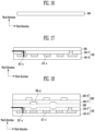
- FIGS. 7 to 17 are cross-sectional views for describing a method of manufacturing the touch sensor shown in FIG.1 .
- FIGS. 7 to 14 are cross-sectional views for describing a method of manufacturing the first substrate
- FIGS. 15 and 16 are cross-sectional views for describing a method of manufacturing the third substrate.
- a method of manufacturing the second substrate may be described with reference to FIGS. 7 to 14 .
- FIG. 7 illustrates steps in forming first protrusions P on a mold M.
- the shape of the first protrusions P may correspond to the shape of the first channels LC1 and the shape of the first grooves of the first groove-formed substrate 100-H, and the material making up the protrusions P may be a material that is photosensitive and stackable to a substantial thickness. For example, SU-8, etc., may be included.
- the mold M may take the shape of a container later in order to hold fluid.
- FIG. 8 illustrates a step in which material making up the first groove-formed substrate 100-H is injected into a mold M with the first protrusions P formed on it, is hardened, and forms the first groove-formed substrate 100-H.
- Material making up the first groove-formed substrate 100-H for example polydimetylsiloxane (PDMS), may flow and be included as a liquid, However, if heat, ultraviolet rays, etc. are applied, material making up the first groove-formed substrate 100-H may be hardened (curing).
- PDMS polydimetylsiloxane
- the first groove-formed substrate 100-H may be formed by putting the material making up the first groove-formed substrate 100-H into a mold M with the shape of a container and with the first protrusions P formed on it and hardening using the eternal environment (heat, ultraviolet rays, etc.). In other words, it may be hardened as the first grooves corresponding to the first protrusions P are formed.
- FIG. 9 illustrates a step in which the first groove-formed substrate 100-H is detached from the mold M. Applying external force onto the first groove-formed substrate 100-H may separate the mold M from the first groove-formed substrate 100-H, and the protrusions from the first groove-formed substrate 100-H.
- the steps shown in FIGS. 7 to 9 may correspond to the steps of forming the first groove-formed substrate 100-H.
- the first grooves H of the first groove-formed substrate 100-H may correspond to the shape of the first protrusions P, and the thickness TH in the third direction of the first grooves H may correspond to the height in the third direction of the first channels LC1.
- FIG. 10 illustrates a step in which liquid material making up the first flat substrate 100-F is poured into the mold M and is hardened.
- Material making up the first flat substrate 100-F may possess the same characteristics as material making up the first groove-formed substrate 100-H. Thus, repeated description may be omitted.
- the first flat substrate 100-F may be formed by pouring the material making up the first flat substrate 100-F into the mold M having the shape of a container and by hardening it by the external environment (heat, ultraviolet rays, etc.) Because the surface of the mold M touching material making up the first groove-formed substrate does not have any protrusions or grooves, the first flat substrate 100-F may have a flat shape.
- FIG. 11 illustrates a step in which the first flat substrate 100-F is detached from the mold M. Just like in the case of the first groove-formed substrate 100-H, application of external force onto the first flat substrate 100-F may separate the mold M and the first flat substrate 100-F.
- the steps shown in FIGS. 10 and 11 may correspond to the step in which the first flat substrate is formed.
- FIG. 12 illustrates a first adherence step in which the first groove-formed substrate 100-H and the first flat substrate 100-F are adhered together to form the first substrate with the first channels formed on it.
- the first groove-formed substrate 100-H and the first flat substrate 100-F may be arranged in such a way that they are touching each other, applied heat to, and adhered together. Or the surface of the first groove-formed substrate 100-H which is to be attached and the surface of the first flat substrate 100-F which is to be attached may be applied with material making up the first groove-formed substrate 100-H before it is hardened.
- the material making up the first groove-formed substrate 100-H may be hardened, and the first groove-formed substrate 100-H and the first flat substrate 100-F may be adhered together.
- the surfaces of the first groove-formed substrate 100-H and the first flat substrate 100-F may be oxygen plasma-treated, and the first groove-formed substrate 100-H and the first flat substrate 100-F may be arranged in such a way that they are touching each other.
- the first channels LC1 may be formed by the first groove-formed substrate 100-H and the first flat substrate 100-F being adhered together.
- FIG. 13 illustrates a step in which first holes and temporary holes are formed in the first channels LC1, and first electrodes are inserted into the first holes.
- the first holes and the temporary holes may be formed in the first channels, and the first electrodes may be inserted into the first holes. Because only the a th first channel LC1-a is shown in FIG. 13 , only a first hole H1-a among all the first holes is shown, only a temporary hole HT-a among all the temporary holes is shown, and only a first electrode EC1-a among all the first electrodes is shown in the figure. Also, in accordance with an exemplary embodiment, the temporary holes may not be formed. In FIG. 13 , the first electrode EC1-a may not be fixed with respect to the first substrate 100. In addition, tubes (not shown) may be inserted into the first and temporary holes to inject the first conductive liquid into or to take air out of the first channels LC1. In this case, the first electrode EC1-a may be provided within one of the tubes.
- FIG. 14 illustrates a step in which the first conductive liquid is injected into the first channels through the first holes and gas is taken out of the first channels through the temporary holes.
- the first conductive liquid from one of the tubes inserted into the first hole H1-a may be injected into the first channel LC1-a.
- the air existent in the first channel LC1-a may be taken out of the first channel LC1-a through one (not shown) of the tubes inserted into the temporary hole HT-a.
- no air may be left in the first channels LC1, making preventing the lowering of the sensitivity of the touch sensor and damage to the touch sensor due to bubbles.
- FIGS. 15 and 16 illustrate a method of manufacturing the third substrate.
- FIG. 15 illustrates a step in which liquefied material making up the third substrate 300 is poured into the mold and hardened. Since this is very similar to the step described with reference to FIG. 10 , in which liquefied material making up the first flat substrate 100-F is poured and hardened is very similar, the description thereof will be omitted.
- Material making up the third substrate 300 and capable of being included in fluid may be put into a mold M with the shape of a container and hardened by the external environment (heat, ultraviolet rays, etc.) to form the third substrate 300.
- the elastic modulus of the third substrate 300 may be lower than those of the first substrate 100 and the second substrate 200.
- the material making up the third substrate 300 for example, PDMS
- the material making up the third substrate 300 may be poured into the mold M and stirred around to form foam.
- other material for example, water
- Hardening material with foam formed may lead to the formation of a porous third substrate 300.
- FIG. 16 illustrates a step in which the third substrate 300 is separated from the mold M.
- the mold M and the third substrate 300 may be separated by applying external force to the third substrate 300.
- FIG. 17 illustrates a third adhesion step in which the first substrate and the third substrate are adhered together.
- the first substrate 100 and the third substrate 300 may be adhered together through the methods described with reference to FIG. 12 .
- the first and the temporary holes may be isolated from outside by the third substrate 300. In other words, the first conductive liquid injected into the first channels LC1 may not come outside.
- the third substrate 300 and the second substrate 200 may be adhered together through the methods described with reference to FIG. 12 .
- the second holes may be isolated from outside by the third substrate 300.
- the second conductive liquid injected into the second channels LC2 may not come outside.
- the touch sensor shown in FIGS. 1 to 3 may be obtained. It may be desirable for the first channels LC1 to extend in the first direction and for the second channels LC2 to extend in the second direction which crosses the first direction. If the third substrate 300 and the second substrate 200 are adhered together, the touch sensor described with reference to FIGS. 1 to 3 may be completed.
- FIG. 18 is a cross-sectional view showing a different example of a touch sensor.
- the touch sensor may include a first substrate 100', a second substrate 200', and a third substrate 300'.
- the third substrate 300' of the touch sensor shown in FIG. 18 may include protrusions 300-p'.
- the degree that the protrusions 300-p' are deformed may be greater than a degree of deformation of the a th first channel LC1-a', in the case a pressure is applied to the touch sensor. Therefore, the risk of a short circuit due to blockage in channels may decrease as the degree to which the first channels LC1-a' are deformed is reduced when the pressure is applied.
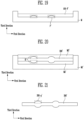
- FIG. 19 is cross-sectional views for describing a method of manufacturing the first flat substrate of the touch sensor of FIG. 18 .
- protrusions P' may be formed on the mold M, and the material making up the first flat substrate 100-F' and which may belong to liquid may be injected and hardened.
- Grooves may be formed on the first flat substrate 100-F', and the shape of the grooves may correspond to the protrusions P' .
- FIG. 20 and FIG. 21 illustrate how to manufacture the third substrate of the touch sensor of FIG. 18 .
- FIG. 20 illustrates a step in which material making up the third substrate 300' is injected between molds M2' and M3' with grooves formed on them and hardened to form the third substrate.
- the material making up the third substrate 300' may be injected among a fixing mold M1' and molds M2' and M3' with grooves H' formed on them. Thereafter, when forming the third substrate 300' by hardening the material, the protrusions corresponding to the grooves H' may be formed on the third substrate 300'.
- FIG. 21 illustrates a step in which the third substrate 300' is separated from the molds M2' and M3'. As described with reference to FIG. 9 , due to applying external force upon the third substrate 300', the third substrate 300' may be separated from the molds M1', M2', and M3'.
- a third substrate with protrusions 300-p' formed on it there are other methods which may be employed to form a third substrate with protrusions 300-p' formed on it.
- grooves may be formed after manufacturing the third substrate.
- FIG. 22 is a cross-sectional view for describing a further example of a touch sensor.
- the first groove-formed substrate 100-H" may include spacers Sp1-a" and Sp2-a". Because the spacers Sp2-a” and Sp2-a” restrict the deformation of the first channels LC1-a", short-circuiting of channels due to excessive applied pressure may be prevented. Also, when pressure is applied to the touch sensor, the amount of change in the thickness of the third substrate 300" may be greater than that of change in the thickness of the first substrate 100" or the second substrate 200". Therefore, the gap between the first channels and the second channels may greatly be changed. Thus the sensitivity to changes in the level of current of voltage incurred by pressure may be increased compared to the touch sensor shown in FIG. 1 .
- FIGS. 23 and 24 are cross-sectional views illustrating some of the methods to manufacture the first groove-formed substrate of the touch sensor of FIG. 22 .
- FIG. 23 illustrates a step in which material making up the first groove-formed substrate 100-H" is injected and hardened to form the first groove-formed substrate 100-H".
- FIG. 23 is mostly identical to FIG. 8 . It is different only in that first protrusions P" are not formed in the part corresponding to the spacers A-sp1" and A-sp2".
- FIG. 24 illustrates a step in which a first groove-formed substrate 100-H" is separated from a mold M".
- FIG. 24 is similar to FIG. 9 , and differs only in that spacers SP1-a" and SP2-a" are formed.
- Exemplary embodiments provide a touch sensor and a method of manufacturing the same which form channels that cross each other on a stretchable substrate, each of the channels including a wedge having a round form. Because a conductive liquid is injected into the channel, touch sensitivity may increase due to the wedge, but because there are no bubbles in the channel, damage to the substrate may be prevented.
Landscapes
- Engineering & Computer Science (AREA)
- General Engineering & Computer Science (AREA)
- Theoretical Computer Science (AREA)
- Microelectronics & Electronic Packaging (AREA)
- Human Computer Interaction (AREA)
- Physics & Mathematics (AREA)
- General Physics & Mathematics (AREA)
- Manufacturing & Machinery (AREA)
- Quality & Reliability (AREA)
- Position Input By Displaying (AREA)
- Manufacture Of Switches (AREA)
Claims (2)
- Capteur tactile comprenant :un premier substrat étirable (100, 100', 100") comprenant des premiers canaux (LC1, LC1-a, LC1-(a+1), LC1-a', LC1-a") étendus dans une première direction ;un premier liquide conducteur injecté dans les premiers canaux (LC1, LC1-a, LC1-(a+1), LC1-a', LC1-a") ;un deuxième substrat étirable (200, 200', 200") comprenant des seconds canaux (LC2, LC2-b) étendus dans une deuxième direction croisant la première direction ; etun second liquide conducteur injecté dans les seconds canaux (LC2, LC2-b)dans lequelle capteur tactile comprend en outre :un troisième substrat étirable (300) agencé entre le premier substrat étirable (100, 100', 100") et le deuxième substrat étirable (200, 200', 200"),dans lequel le module d'élasticité du troisième substrat étirable (300) est inférieur à ceux du premier et du deuxième substrat étirable (100, 100', 100", 200, 200', 200"),le premier substrat étirable (100, 100', 100") inclut un premier substrat formé de rainures (100-H) et un premier substrat plat (100-F), et le deuxième substrat étirable (200, 200', 200") inclut un second substrat formé de rainures (200-H) et un second substrat plat (200-F),chaque premier canal (LC1, LC1-a, LC1-(a+1), LC1-a', LC1-a") comporte une première électrode (EC1-a, EC1-(a+1)) agencée entre le premier substrat plat (100-F) et le troisième substrat étirable (300),chaque second canal (LC2, LC2-b) comporte une seconde électrode (EC2-b) agencée entre le second substrat plat (200-F) et le troisième substrat étirable (300),les premières électrodes (EC1-a, EC1-(a+1)) sont en contact avec le premier liquide conducteur et les secondes électrodes (EC2-b) sont en contact avec le second liquide conducteur ;les premières électrodes (EC1-a, EC1-(a+1)) sont conçues pour fournir une tension ou un courant et les secondes électrodes (EC2-b) sont conçues pour mesurer des changements de niveaux de la tension ou du courant,dans lequel le premier substrat étirable (100, 100', 100"), le deuxième substrat étirable (200, 200', 200") et le troisième substrat étirable (300) ont une épaisseur dans une troisième direction qui croise à la fois la première et la deuxième direction,les premiers canaux (LC1, LC1-a, LC1-(a+1), LC1-a', LC1-a'') et les seconds canaux (LC2, LC2-b) comprennent des canaux droits (LC1-a-s-1, LC1-a-s-2, LC2-b-s-1, LC2-b-s-2) et des coins (LC1-a-w-1, LC2-b-w-1, LC2-b-w-2),dans lequel les canaux droits (LC1-a-s-1, LC1-a-s-2) des premiers canaux (LC1, LC1-a, LC1-(a+1), LC1-a', LC1-a") ont une largeur W dans la première direction et chaque paire de canaux adjacents des canaux droits (LC1-a-s-1, LC1-a-s-2) sont reliés par un des coins (LC1-a-w-1), etchaque coin (LC1-a-w-1) comprend une partie ronde, dans lequel les canaux droits (LC2-b-s-1, LC2-b-s-2) des seconds canaux (LC2, LC2-b) ont une largeur W dans la deuxième direction et chaque paire de canaux adjacents des canaux droits (LC2-a-s-2) sont reliés par un des coins (LC2-b-w-1, LC2-b-w-2), et chaque coin (LC2-b-w-1, LC2-b-w-2) comprend une partie ronde,les canaux droits (LC1-a-s-1, LC1-a-s-2, LC2-b-s-1, LC2-b-s-2) et les coins (LC1-a-w-1, LC2-b-w-1, LC2-b-w-2) sont agencés dans un plan défini par les première et deuxième directions, etchaque partie ronde comprend une portion ronde interne (R-I) disposée au niveau d'un bord intérieur des deux canaux droits adjacents (LC1-a-s-1, LC1-a-s-2) reliés par ledit un coin (LC1-a-w-1) et une portion ronde externe (R-O) formant l'extrémité étroite dudit un coin (LC1-a-w-1) ; etun rayon de courbure (ROC) de la portion ronde externe (R-O) est exprimé dans une équation ci-dessous :
 où W est la largeur des canaux droits (LC1-a-s-1, LC1-a-s-2, LC2-b-s-1, LC2-b-s-2) et ROC-O est le rayon de la courbure (ROC) de la portion ronde externe (R-O),dans lequel le contour interne du coin (LC1-a-w-1) à l'extrémité étroite et dans la région reliant les canaux droits débouchant dans le coin est continu,les coins (LC1-a-w-1) des premiers canaux (LC1, LC1-a, LC1-(a+1), LC1-a', LC1-a") ont une longueur (L) dans la deuxième direction et les coins (LC2-b-w-1, LC2-b-w-2) des seconds canaux (LC2, LC2-b) ont la longueur (L) dans la première direction,dans lequel la longueur (L) des coins des premiers canaux (LC1, LC1-a, LC1-(a+1), LC1-a', LC1-a") est supérieure ou égale à 150 µm et inférieure ou égale à 600 µm, etdans lequel la longueur (L) des coins des seconds canaux (LC2, LC2-b) est supérieure ou égale à 150 µm et inférieure ou égale à 600 pm,dans lequel une distance (D) entre des coins adjacents de canaux adjacents est dans une plage supérieure ou égale à 150 µm et inférieure ou égale à 200 µm.
 - Procédé de fabrication d'un capteur tactile selon la revendication 1.
Priority Applications (1)
| Application Number | Priority Date | Filing Date | Title |
|---|---|---|---|
| EP18170474.3A EP3373121B1 (fr) | 2015-08-28 | 2016-08-05 | Capteur de gaz et son procédé de fabrication |
Applications Claiming Priority (1)
| Application Number | Priority Date | Filing Date | Title |
|---|---|---|---|
| KR1020150121938A KR102420052B1 (ko) | 2015-08-28 | 2015-08-28 | 터치 센서 및 그 제작 방법 |
Related Child Applications (2)
| Application Number | Title | Priority Date | Filing Date |
|---|---|---|---|
| EP18170474.3A Division EP3373121B1 (fr) | 2015-08-28 | 2016-08-05 | Capteur de gaz et son procédé de fabrication |
| EP18170474.3A Division-Into EP3373121B1 (fr) | 2015-08-28 | 2016-08-05 | Capteur de gaz et son procédé de fabrication |
Publications (3)
| Publication Number | Publication Date |
|---|---|
| EP3144787A2 EP3144787A2 (fr) | 2017-03-22 |
| EP3144787A3 EP3144787A3 (fr) | 2017-07-05 |
| EP3144787B1 true EP3144787B1 (fr) | 2023-09-20 |
Family
ID=56737915
Family Applications (2)
| Application Number | Title | Priority Date | Filing Date |
|---|---|---|---|
| EP18170474.3A Active EP3373121B1 (fr) | 2015-08-28 | 2016-08-05 | Capteur de gaz et son procédé de fabrication |
| EP16182915.5A Active EP3144787B1 (fr) | 2015-08-28 | 2016-08-05 | Capteur de gaz et procédé de fabrication de celui-ci |
Family Applications Before (1)
| Application Number | Title | Priority Date | Filing Date |
|---|---|---|---|
| EP18170474.3A Active EP3373121B1 (fr) | 2015-08-28 | 2016-08-05 | Capteur de gaz et son procédé de fabrication |
Country Status (4)
| Country | Link |
|---|---|
| US (2) | US10558303B2 (fr) |
| EP (2) | EP3373121B1 (fr) |
| JP (1) | JP6770327B2 (fr) |
| KR (1) | KR102420052B1 (fr) |
Families Citing this family (5)
| Publication number | Priority date | Publication date | Assignee | Title |
|---|---|---|---|---|
| KR102420052B1 (ko) * | 2015-08-28 | 2022-07-14 | 삼성디스플레이 주식회사 | 터치 센서 및 그 제작 방법 |
| KR102594615B1 (ko) | 2017-12-13 | 2023-10-30 | 삼성디스플레이 주식회사 | 입력감지유닛 및 이를 포함하는 표시장치 |
| CN109326221B (zh) * | 2018-09-25 | 2021-09-28 | 上海天马微电子有限公司 | 显示装置和显示装置的触觉反馈显示方法 |
| CN109638043A (zh) * | 2018-12-03 | 2019-04-16 | 武汉华星光电半导体显示技术有限公司 | 柔性有机发光二极管(oled)显示基板及其制作方法 |
| US11017915B2 (en) * | 2019-01-23 | 2021-05-25 | Carnegie Mellon University | Stretchable electronics and methods of making the same |
Family Cites Families (12)
| Publication number | Priority date | Publication date | Assignee | Title |
|---|---|---|---|---|
| DE202007005237U1 (de) * | 2006-04-25 | 2007-07-05 | Philipp, Harald, Southampton | Hybrides kapazitives Berührungsbildschirmelement |
| US20140152611A1 (en) | 2012-06-01 | 2014-06-05 | Tactus Technology, Inc. | User interface |
| US8970403B2 (en) * | 2008-01-04 | 2015-03-03 | Tactus Technology, Inc. | Method for actuating a tactile interface layer |
| JP5606242B2 (ja) * | 2010-09-24 | 2014-10-15 | 株式会社ジャパンディスプレイ | 表示装置 |
| WO2012103073A2 (fr) * | 2011-01-24 | 2012-08-02 | President And Fellows Of Harvard College | Détecteur de courbure élastomère sans mesure des différences de déformation |
| EP2758760B1 (fr) * | 2011-09-24 | 2021-02-17 | President and Fellows of Harvard College | Capteur de déformation élastique |
| US9239346B2 (en) * | 2012-01-28 | 2016-01-19 | The Regents Of The University Of California | Systems for providing electro-mechanical sensors |
| KR101585934B1 (ko) | 2013-04-03 | 2016-01-15 | 어보브반도체 주식회사 | 정전용량 방식 터치패널 |
| WO2015048530A1 (fr) * | 2013-09-26 | 2015-04-02 | Tactus Technology, Inc. | Capteur tactile |
| KR102199213B1 (ko) | 2014-03-03 | 2021-01-07 | 삼성디스플레이 주식회사 | 터치 패널 및 이를 포함하는 표시 장치 |
| KR102244435B1 (ko) | 2014-09-03 | 2021-04-26 | 삼성디스플레이 주식회사 | 회로판 및 이를 포함하는 전자 장치 |
| KR102420052B1 (ko) * | 2015-08-28 | 2022-07-14 | 삼성디스플레이 주식회사 | 터치 센서 및 그 제작 방법 |
-
2015
- 2015-08-28 KR KR1020150121938A patent/KR102420052B1/ko active Active
-
2016
- 2016-03-17 US US15/072,958 patent/US10558303B2/en active Active
- 2016-04-05 JP JP2016075667A patent/JP6770327B2/ja active Active
- 2016-08-05 EP EP18170474.3A patent/EP3373121B1/fr active Active
- 2016-08-05 EP EP16182915.5A patent/EP3144787B1/fr active Active
-
2020
- 2020-02-10 US US16/785,695 patent/US11086465B2/en active Active
Also Published As
| Publication number | Publication date |
|---|---|
| EP3144787A2 (fr) | 2017-03-22 |
| US20170060299A1 (en) | 2017-03-02 |
| JP2017045439A (ja) | 2017-03-02 |
| EP3373121B1 (fr) | 2023-09-20 |
| EP3144787A3 (fr) | 2017-07-05 |
| US11086465B2 (en) | 2021-08-10 |
| KR102420052B1 (ko) | 2022-07-14 |
| KR20170026820A (ko) | 2017-03-09 |
| JP6770327B2 (ja) | 2020-10-14 |
| US20200174600A1 (en) | 2020-06-04 |
| EP3373121A1 (fr) | 2018-09-12 |
| US10558303B2 (en) | 2020-02-11 |
Similar Documents
| Publication | Publication Date | Title |
|---|---|---|
| EP3144787B1 (fr) | Capteur de gaz et procédé de fabrication de celui-ci | |
| US9228822B2 (en) | Non-differential elastomer curvature sensor | |
| KR102211497B1 (ko) | 촉각 디스플레이 장치 | |
| US10229564B2 (en) | Apparatus and methods for providing tactile stimulus incorporating tri-layer actuators | |
| KR102655316B1 (ko) | 불균일 공간 전하층과 유전성 유체를 이용한 주머니 형태의 유연 구동기 | |
| Tsouti et al. | Modeling and development of a flexible carbon black-based capacitive strain sensor | |
| Majidi et al. | A non-differential elastomer curvature sensor for softer-than-skin electronics | |
| Tabatabai et al. | Liquid-phase gallium–indium alloy electronics with microcontact printing | |
| US9645028B2 (en) | Resistive pressure sensor including piezo-resistive electrode | |
| KR102668666B1 (ko) | 전단력을 산출할 수 있는 정전용량 검출장치 | |
| EP3979487A1 (fr) | Actionneur électrostatique empilé | |
| CN107431059B (zh) | 用于可变形电子装置的阿基米德螺线设计 | |
| TW201917923A (zh) | 彎曲極限薄膜 | |
| Pineda et al. | Using electrofluidic devices as hyper-elastic strain sensors: Experimental and theoretical analysis | |
| EP3004828B1 (fr) | Un capteur de pression amélioré | |
| KR102721873B1 (ko) | 유연 조인트 구조가 도입된 오그제틱 신축성 기판 및 그 제조 방법 | |
| KR20170126302A (ko) | 압력 센서 소자 및 압력 센서 소자 제조 방법 | |
| Balakrisnan et al. | Design of compliant meanders for applications in MEMS, actuators, and flexible electronics | |
| Zhou et al. | A novel liquid metal sensor with three microchannels embedded in elastomer | |
| Zhou et al. | Three-layer-stacked pressure sensor with a liquid metal-embedded elastomer | |
| Jang et al. | Fabrication of highly sensitive piezocapacitive pressure sensors using a simple and inexpensive home milk frother | |
| US20190204943A1 (en) | Protective cover of touch key structure, method of fabrication thereof, and touch panel with covered touch key structure | |
| US20240161862A1 (en) | Smart mechanical metamaterials with tunable stimuli-responsive expansion coefficients | |
| US20250299890A1 (en) | Capacitor element | |
| EP3009822B1 (fr) | Appareil et procédé de déformable |
Legal Events
| Date | Code | Title | Description |
|---|---|---|---|
| PUAI | Public reference made under article 153(3) epc to a published international application that has entered the european phase |
Free format text: ORIGINAL CODE: 0009012 |
|
| STAA | Information on the status of an ep patent application or granted ep patent |
Free format text: STATUS: THE APPLICATION HAS BEEN PUBLISHED |
|
| AK | Designated contracting states |
Kind code of ref document: A2 Designated state(s): AL AT BE BG CH CY CZ DE DK EE ES FI FR GB GR HR HU IE IS IT LI LT LU LV MC MK MT NL NO PL PT RO RS SE SI SK SM TR |
|
| AX | Request for extension of the european patent |
Extension state: BA ME |
|
| PUAL | Search report despatched |
Free format text: ORIGINAL CODE: 0009013 |
|
| AK | Designated contracting states |
Kind code of ref document: A3 Designated state(s): AL AT BE BG CH CY CZ DE DK EE ES FI FR GB GR HR HU IE IS IT LI LT LU LV MC MK MT NL NO PL PT RO RS SE SI SK SM TR |
|
| AX | Request for extension of the european patent |
Extension state: BA ME |
|
| RIC1 | Information provided on ipc code assigned before grant |
Ipc: G06F 3/044 20060101AFI20170530BHEP |
|
| STAA | Information on the status of an ep patent application or granted ep patent |
Free format text: STATUS: REQUEST FOR EXAMINATION WAS MADE |
|
| 17P | Request for examination filed |
Effective date: 20171130 |
|
| RBV | Designated contracting states (corrected) |
Designated state(s): AL AT BE BG CH CY CZ DE DK EE ES FI FR GB GR HR HU IE IS IT LI LT LU LV MC MK MT NL NO PL PT RO RS SE SI SK SM TR |
|
| STAA | Information on the status of an ep patent application or granted ep patent |
Free format text: STATUS: EXAMINATION IS IN PROGRESS |
|
| 17Q | First examination report despatched |
Effective date: 20210304 |
|
| GRAP | Despatch of communication of intention to grant a patent |
Free format text: ORIGINAL CODE: EPIDOSNIGR1 |
|
| STAA | Information on the status of an ep patent application or granted ep patent |
Free format text: STATUS: GRANT OF PATENT IS INTENDED |
|
| INTG | Intention to grant announced |
Effective date: 20230331 |
|
| P01 | Opt-out of the competence of the unified patent court (upc) registered |
Effective date: 20230515 |
|
| GRAS | Grant fee paid |
Free format text: ORIGINAL CODE: EPIDOSNIGR3 |
|
| GRAA | (expected) grant |
Free format text: ORIGINAL CODE: 0009210 |
|
| STAA | Information on the status of an ep patent application or granted ep patent |
Free format text: STATUS: THE PATENT HAS BEEN GRANTED |
|
| AK | Designated contracting states |
Kind code of ref document: B1 Designated state(s): AL AT BE BG CH CY CZ DE DK EE ES FI FR GB GR HR HU IE IS IT LI LT LU LV MC MK MT NL NO PL PT RO RS SE SI SK SM TR |
|
| REG | Reference to a national code |
Ref country code: GB Ref legal event code: FG4D |
|
| REG | Reference to a national code |
Ref country code: CH Ref legal event code: EP |
|
| REG | Reference to a national code |
Ref country code: IE Ref legal event code: FG4D |
|
| REG | Reference to a national code |
Ref country code: DE Ref legal event code: R096 Ref document number: 602016082866 Country of ref document: DE |
|
| REG | Reference to a national code |
Ref country code: LT Ref legal event code: MG9D |
|
| PG25 | Lapsed in a contracting state [announced via postgrant information from national office to epo] |
Ref country code: GR Free format text: LAPSE BECAUSE OF FAILURE TO SUBMIT A TRANSLATION OF THE DESCRIPTION OR TO PAY THE FEE WITHIN THE PRESCRIBED TIME-LIMIT Effective date: 20231221 |
|
| REG | Reference to a national code |
Ref country code: NL Ref legal event code: MP Effective date: 20230920 |
|
| PG25 | Lapsed in a contracting state [announced via postgrant information from national office to epo] |
Ref country code: SE Free format text: LAPSE BECAUSE OF FAILURE TO SUBMIT A TRANSLATION OF THE DESCRIPTION OR TO PAY THE FEE WITHIN THE PRESCRIBED TIME-LIMIT Effective date: 20230920 Ref country code: RS Free format text: LAPSE BECAUSE OF FAILURE TO SUBMIT A TRANSLATION OF THE DESCRIPTION OR TO PAY THE FEE WITHIN THE PRESCRIBED TIME-LIMIT Effective date: 20230920 Ref country code: NO Free format text: LAPSE BECAUSE OF FAILURE TO SUBMIT A TRANSLATION OF THE DESCRIPTION OR TO PAY THE FEE WITHIN THE PRESCRIBED TIME-LIMIT Effective date: 20231220 Ref country code: LV Free format text: LAPSE BECAUSE OF FAILURE TO SUBMIT A TRANSLATION OF THE DESCRIPTION OR TO PAY THE FEE WITHIN THE PRESCRIBED TIME-LIMIT Effective date: 20230920 Ref country code: LT Free format text: LAPSE BECAUSE OF FAILURE TO SUBMIT A TRANSLATION OF THE DESCRIPTION OR TO PAY THE FEE WITHIN THE PRESCRIBED TIME-LIMIT Effective date: 20230920 Ref country code: HR Free format text: LAPSE BECAUSE OF FAILURE TO SUBMIT A TRANSLATION OF THE DESCRIPTION OR TO PAY THE FEE WITHIN THE PRESCRIBED TIME-LIMIT Effective date: 20230920 Ref country code: GR Free format text: LAPSE BECAUSE OF FAILURE TO SUBMIT A TRANSLATION OF THE DESCRIPTION OR TO PAY THE FEE WITHIN THE PRESCRIBED TIME-LIMIT Effective date: 20231221 Ref country code: FI Free format text: LAPSE BECAUSE OF FAILURE TO SUBMIT A TRANSLATION OF THE DESCRIPTION OR TO PAY THE FEE WITHIN THE PRESCRIBED TIME-LIMIT Effective date: 20230920 |
|
| REG | Reference to a national code |
Ref country code: AT Ref legal event code: MK05 Ref document number: 1613907 Country of ref document: AT Kind code of ref document: T Effective date: 20230920 |
|
| PG25 | Lapsed in a contracting state [announced via postgrant information from national office to epo] |
Ref country code: NL Free format text: LAPSE BECAUSE OF FAILURE TO SUBMIT A TRANSLATION OF THE DESCRIPTION OR TO PAY THE FEE WITHIN THE PRESCRIBED TIME-LIMIT Effective date: 20230920 |
|
| PG25 | Lapsed in a contracting state [announced via postgrant information from national office to epo] |
Ref country code: IS Free format text: LAPSE BECAUSE OF FAILURE TO SUBMIT A TRANSLATION OF THE DESCRIPTION OR TO PAY THE FEE WITHIN THE PRESCRIBED TIME-LIMIT Effective date: 20240120 |
|
| PG25 | Lapsed in a contracting state [announced via postgrant information from national office to epo] |
Ref country code: AT Free format text: LAPSE BECAUSE OF FAILURE TO SUBMIT A TRANSLATION OF THE DESCRIPTION OR TO PAY THE FEE WITHIN THE PRESCRIBED TIME-LIMIT Effective date: 20230920 |
|
| PG25 | Lapsed in a contracting state [announced via postgrant information from national office to epo] |
Ref country code: ES Free format text: LAPSE BECAUSE OF FAILURE TO SUBMIT A TRANSLATION OF THE DESCRIPTION OR TO PAY THE FEE WITHIN THE PRESCRIBED TIME-LIMIT Effective date: 20230920 |
|
| PG25 | Lapsed in a contracting state [announced via postgrant information from national office to epo] |
Ref country code: SM Free format text: LAPSE BECAUSE OF FAILURE TO SUBMIT A TRANSLATION OF THE DESCRIPTION OR TO PAY THE FEE WITHIN THE PRESCRIBED TIME-LIMIT Effective date: 20230920 Ref country code: RO Free format text: LAPSE BECAUSE OF FAILURE TO SUBMIT A TRANSLATION OF THE DESCRIPTION OR TO PAY THE FEE WITHIN THE PRESCRIBED TIME-LIMIT Effective date: 20230920 Ref country code: IS Free format text: LAPSE BECAUSE OF FAILURE TO SUBMIT A TRANSLATION OF THE DESCRIPTION OR TO PAY THE FEE WITHIN THE PRESCRIBED TIME-LIMIT Effective date: 20240120 Ref country code: ES Free format text: LAPSE BECAUSE OF FAILURE TO SUBMIT A TRANSLATION OF THE DESCRIPTION OR TO PAY THE FEE WITHIN THE PRESCRIBED TIME-LIMIT Effective date: 20230920 Ref country code: EE Free format text: LAPSE BECAUSE OF FAILURE TO SUBMIT A TRANSLATION OF THE DESCRIPTION OR TO PAY THE FEE WITHIN THE PRESCRIBED TIME-LIMIT Effective date: 20230920 Ref country code: CZ Free format text: LAPSE BECAUSE OF FAILURE TO SUBMIT A TRANSLATION OF THE DESCRIPTION OR TO PAY THE FEE WITHIN THE PRESCRIBED TIME-LIMIT Effective date: 20230920 Ref country code: AT Free format text: LAPSE BECAUSE OF FAILURE TO SUBMIT A TRANSLATION OF THE DESCRIPTION OR TO PAY THE FEE WITHIN THE PRESCRIBED TIME-LIMIT Effective date: 20230920 Ref country code: SK Free format text: LAPSE BECAUSE OF FAILURE TO SUBMIT A TRANSLATION OF THE DESCRIPTION OR TO PAY THE FEE WITHIN THE PRESCRIBED TIME-LIMIT Effective date: 20230920 Ref country code: PT Free format text: LAPSE BECAUSE OF FAILURE TO SUBMIT A TRANSLATION OF THE DESCRIPTION OR TO PAY THE FEE WITHIN THE PRESCRIBED TIME-LIMIT Effective date: 20240122 |
|
| PG25 | Lapsed in a contracting state [announced via postgrant information from national office to epo] |
Ref country code: PL Free format text: LAPSE BECAUSE OF FAILURE TO SUBMIT A TRANSLATION OF THE DESCRIPTION OR TO PAY THE FEE WITHIN THE PRESCRIBED TIME-LIMIT Effective date: 20230920 Ref country code: IT Free format text: LAPSE BECAUSE OF FAILURE TO SUBMIT A TRANSLATION OF THE DESCRIPTION OR TO PAY THE FEE WITHIN THE PRESCRIBED TIME-LIMIT Effective date: 20230920 |
|
| REG | Reference to a national code |
Ref country code: DE Ref legal event code: R097 Ref document number: 602016082866 Country of ref document: DE |
|
| PG25 | Lapsed in a contracting state [announced via postgrant information from national office to epo] |
Ref country code: DK Free format text: LAPSE BECAUSE OF FAILURE TO SUBMIT A TRANSLATION OF THE DESCRIPTION OR TO PAY THE FEE WITHIN THE PRESCRIBED TIME-LIMIT Effective date: 20230920 |
|
| PLBE | No opposition filed within time limit |
Free format text: ORIGINAL CODE: 0009261 |
|
| STAA | Information on the status of an ep patent application or granted ep patent |
Free format text: STATUS: NO OPPOSITION FILED WITHIN TIME LIMIT |
|
| PG25 | Lapsed in a contracting state [announced via postgrant information from national office to epo] |
Ref country code: DK Free format text: LAPSE BECAUSE OF FAILURE TO SUBMIT A TRANSLATION OF THE DESCRIPTION OR TO PAY THE FEE WITHIN THE PRESCRIBED TIME-LIMIT Effective date: 20230920 |
|
| 26N | No opposition filed |
Effective date: 20240621 |
|
| PG25 | Lapsed in a contracting state [announced via postgrant information from national office to epo] |
Ref country code: SI Free format text: LAPSE BECAUSE OF FAILURE TO SUBMIT A TRANSLATION OF THE DESCRIPTION OR TO PAY THE FEE WITHIN THE PRESCRIBED TIME-LIMIT Effective date: 20230920 |
|
| PG25 | Lapsed in a contracting state [announced via postgrant information from national office to epo] |
Ref country code: SI Free format text: LAPSE BECAUSE OF FAILURE TO SUBMIT A TRANSLATION OF THE DESCRIPTION OR TO PAY THE FEE WITHIN THE PRESCRIBED TIME-LIMIT Effective date: 20230920 |
|
| PG25 | Lapsed in a contracting state [announced via postgrant information from national office to epo] |
Ref country code: BG Free format text: LAPSE BECAUSE OF FAILURE TO SUBMIT A TRANSLATION OF THE DESCRIPTION OR TO PAY THE FEE WITHIN THE PRESCRIBED TIME-LIMIT Effective date: 20230920 |
|
| PG25 | Lapsed in a contracting state [announced via postgrant information from national office to epo] |
Ref country code: BG Free format text: LAPSE BECAUSE OF FAILURE TO SUBMIT A TRANSLATION OF THE DESCRIPTION OR TO PAY THE FEE WITHIN THE PRESCRIBED TIME-LIMIT Effective date: 20230920 |
|
| REG | Reference to a national code |
Ref country code: CH Ref legal event code: PL |
|
| PG25 | Lapsed in a contracting state [announced via postgrant information from national office to epo] |
Ref country code: LU Free format text: LAPSE BECAUSE OF NON-PAYMENT OF DUE FEES Effective date: 20240805 |
|
| PG25 | Lapsed in a contracting state [announced via postgrant information from national office to epo] |
Ref country code: CH Free format text: LAPSE BECAUSE OF NON-PAYMENT OF DUE FEES Effective date: 20240831 Ref country code: MC Free format text: LAPSE BECAUSE OF FAILURE TO SUBMIT A TRANSLATION OF THE DESCRIPTION OR TO PAY THE FEE WITHIN THE PRESCRIBED TIME-LIMIT Effective date: 20230920 |
|
| REG | Reference to a national code |
Ref country code: BE Ref legal event code: MM Effective date: 20240831 |
|
| PG25 | Lapsed in a contracting state [announced via postgrant information from national office to epo] |
Ref country code: BE Free format text: LAPSE BECAUSE OF NON-PAYMENT OF DUE FEES Effective date: 20240831 |
|
| PG25 | Lapsed in a contracting state [announced via postgrant information from national office to epo] |
Ref country code: IE Free format text: LAPSE BECAUSE OF NON-PAYMENT OF DUE FEES Effective date: 20240805 |
|
| PGFP | Annual fee paid to national office [announced via postgrant information from national office to epo] |
Ref country code: DE Payment date: 20250721 Year of fee payment: 10 |
|
| PGFP | Annual fee paid to national office [announced via postgrant information from national office to epo] |
Ref country code: GB Payment date: 20250722 Year of fee payment: 10 |
|
| PGFP | Annual fee paid to national office [announced via postgrant information from national office to epo] |
Ref country code: FR Payment date: 20250725 Year of fee payment: 10 |
|
| PG25 | Lapsed in a contracting state [announced via postgrant information from national office to epo] |
Ref country code: CY Free format text: LAPSE BECAUSE OF FAILURE TO SUBMIT A TRANSLATION OF THE DESCRIPTION OR TO PAY THE FEE WITHIN THE PRESCRIBED TIME-LIMIT; INVALID AB INITIO Effective date: 20160805 |
|
| PG25 | Lapsed in a contracting state [announced via postgrant information from national office to epo] |
Ref country code: HU Free format text: LAPSE BECAUSE OF FAILURE TO SUBMIT A TRANSLATION OF THE DESCRIPTION OR TO PAY THE FEE WITHIN THE PRESCRIBED TIME-LIMIT; INVALID AB INITIO Effective date: 20160805 |