EP3144937B1 - Décodeur de rangée pour un dispositif de mémoire non volatile, possédant une zone réduite d'occupation - Google Patents
Décodeur de rangée pour un dispositif de mémoire non volatile, possédant une zone réduite d'occupation Download PDFInfo
- Publication number
- EP3144937B1 EP3144937B1 EP16161883.0A EP16161883A EP3144937B1 EP 3144937 B1 EP3144937 B1 EP 3144937B1 EP 16161883 A EP16161883 A EP 16161883A EP 3144937 B1 EP3144937 B1 EP 3144937B1
- Authority
- EP
- European Patent Office
- Prior art keywords
- address signals
- input
- combined
- sxyhv
- psxhvn
- Prior art date
- Legal status (The legal status is an assumption and is not a legal conclusion. Google has not performed a legal analysis and makes no representation as to the accuracy of the status listed.)
- Active
Links
Images


Classifications
-
- G—PHYSICS
- G11—INFORMATION STORAGE
- G11C—STATIC STORES
- G11C16/00—Erasable programmable read-only memories
- G11C16/02—Erasable programmable read-only memories electrically programmable
- G11C16/06—Auxiliary circuits, e.g. for writing into memory
- G11C16/08—Address circuits; Decoders; Word-line control circuits
-
- G—PHYSICS
- G11—INFORMATION STORAGE
- G11C—STATIC STORES
- G11C16/00—Erasable programmable read-only memories
- G11C16/02—Erasable programmable read-only memories electrically programmable
- G11C16/06—Auxiliary circuits, e.g. for writing into memory
- G11C16/10—Programming or data input circuits
-
- G—PHYSICS
- G11—INFORMATION STORAGE
- G11C—STATIC STORES
- G11C16/00—Erasable programmable read-only memories
- G11C16/02—Erasable programmable read-only memories electrically programmable
- G11C16/06—Auxiliary circuits, e.g. for writing into memory
- G11C16/24—Bit-line control circuits
-
- G—PHYSICS
- G11—INFORMATION STORAGE
- G11C—STATIC STORES
- G11C8/00—Arrangements for selecting an address in a digital store
- G11C8/10—Decoders
Definitions
- the present invention relates to a row decoder, having a reduced area occupation, for a non-volatile memory device, in particular of a flash type, for addressing and biasing rows of the corresponding memory array.
- a non-volatile memory device designated by 1, for example of a NAND or NOR flash type, generally comprises a memory array 2 made up of a plurality of memory cells 3, arranged in rows (wordlines WL) and columns (bitlines BL).
- Each memory cell 3 is constituted by a storage element formed by a floating-gate transistor, with its gate terminal designed to be coupled to a respective wordline WL, a first conduction terminal designed to be coupled to a respective bitline BL, and a second conduction terminal connected to a reference potential (for example, ground GND).
- a reference potential for example, ground GND
- the memory array 2 is generally arranged in a plurality of sectors, each of which comprises a plurality of memory cells 3. Each sector has a plurality of respective wordlines WL, distinct from those of the other sectors and physically connected to the memory cells 3 present in the same sector.
- a column decoder 4 and a row decoder 5 allow selection, on the basis of address signals received at input (generated in a per se known manner and designated as a whole by AS - "Address Signal", AS r for the rows, and AS c for the columns), of the memory cells 3, and in particular of the corresponding wordlines WL and bitlines BL each time addressed in the various sectors, enabling biasing thereof at appropriate voltage and current values during memory operations.
- the column decoder 4 may further be configured to provide internally two paths towards the bitlines BL of the memory array 2 each time selected: a reading path, for defining a conductive path between the selected bitline BL and a sense-amplifier stage 7, designed to compare the current flowing in the addressed memory cell 3 with a reference current in order to determine the datum stored; and a programming path, for creating a conductive path between the selected bitline BL and a driving stage 8, configured to supply the required biasing quantities.
- non-volatile memories of a flash type it is known that memory operations require high values of the biasing voltage applied to the wordlines WL, for example a boosted voltage (high voltage, HV) of 4.5 V, during reading operations.
- HV high voltage
- These values of the biasing voltages are generated within the memory device by charge-pump stages, which generate a boosted voltage starting from a supply voltage Vdd with logic value, for example a low voltage (LV) of 1.2 V.
- the row decoder 5 thus usually has a configuration with a low-voltage portion (i.e., a portion operating with voltages in the region of the supply voltage V dd , for example 1.2 V) and a high-voltage portion (i.e., a portion operating in the high-voltage range, i.e., with voltages in the region of the boosted voltage, for example 4.5 V), which is to be coupled to the wordlines WL of the memory array 2 for supplying the required biasing quantities.
- Level shifters are used for shifting the low-voltage signals (for example, 1.2 V) of the first portion of the row decoder 5 to high-voltage signals (for example, 4.5 V) of the second portion of the row decoder 5.
- the row decoder 5 comprises an input module 10, which receives the row address signals AS r , digital signals having a certain number of bits, from an input-address bus 11, and appropriately groups together the bits of the same row address signals AS r into subsets, in order to generate low-voltage grouped address signals PAS LV .
- the row decoder 5 further comprises a pre-decoding module 12, which receives the grouped address signals PAS LV and combines them logically in an appropriate way, to generate low-voltage pre-decoded address signals PAS LV , on a first transport bus 13, which includes a certain number of lines, each of which corresponding to a respective combination of the grouped address signals PAS LV .
- the low-voltage pre-decoded address signals PAS LV then reach a voltage-booster module 14, which receives at input the low-voltage pre-decoded address signals PAS LV and generates high-voltage pre-decoded address signals PAS HV on a second transport bus 15, which includes a number of lines corresponding to the number of lines of the first transport bus 13.
- the row decoder 5 further comprises: a decoding module 16, which receives the pre-decoded address signals PAS HV and combines them logically in an appropriate way for generating decoded address signals DAS HV , which are also high-voltage signals, on an output bus 17, which includes a number of lines corresponding to the number of wordlines WL of the addressed sector of the memory array 2; and a driving module 18, which receives the decoded address signals DAS HV from the output bus 17 and generates appropriate high-voltage biasing signals S_WL for the respective wordlines WL of the sector of the memory array 2, so as to perform addressing and biasing of the corresponding memory cells 3.
- a decoding module 16 which receives the pre-decoded address signals PAS HV and combines them logically in an appropriate way for generating decoded address signals DAS HV , which are also high-voltage signals, on an output bus 17, which includes a number of lines corresponding to the number of wordlines WL of the addressed sector of the memory array 2;
- Row-decoder architectures 5 substantially similar to what described above are illustrated for example in:
- the row address signals AS r (for example, nine-bit digital signals) are received by the input module 10 of the row decoder 5 and grouped appropriately into subsets in order to generate the grouped address signals PAS LV , here designated by way of example as: px (referred to in what follows “as first address signals”), lx (referred to in what follows as “second address signals”) and ly (referred to in what follows as "third address signals").
- the first address signals px may correspond to the three bits AS r ⁇ 8:10>
- the second address signals ly may correspond to the two bits AS r ⁇ 11:12>
- the third address signals lx may correspond to the remaining four bits AS r ⁇ 13:16>.
- the input stage 10 further generates, based on the row address signals AS r , fourth address signals Is.
- the fourth address signals ls may indicate the sector of the memory array 2 that is to be selected
- the first address signals px may indicate a block (in the example, of eight wordlines WL) to be addressed within the sector
- the second and third address signals lx and ly may indicate the specific wordlines WL to be addressed within the selected block.
- the pre-decoding module 12 comprises a plurality of first logic gates 24, of a two-input, one-output NAND type, each of which receives at the inputs a respective first address signal px and a respective fourth address signal ls and supplies at the output a respective first low-voltage pre-decoded address signal, here designated by psx.
- the first logic gates 24 are eight in number (i.e., in a number equal to the number of combinations that may be obtained starting from the address signals received at the input).
- the pre-decoding module 12 further comprises a plurality of second logic gates 25, of a three-input, one-output NAND type, each of which receives at the inputs a respective second address signal lx, a respective third address signal ly, and a respective fourth address signal Is, and supplies at the output a second low-voltage pre-decoded address signal, here designated by sxy.
- the second logic gates 25 are sixty-four in number (i.e., once again in a number equal to the number of combinations that may be obtained starting from the address signals received at the input).
- the first transport bus 13 comprises in this case eight lines for the first low-voltage pre-decoded address signals psx, and sixty-four lines for the second low-voltage pre-decoded address signals sxy, which are received at the input of the booster module 14.
- the booster module 14 comprises a plurality of first booster stages 26, each having an input that receives a respective first low-voltage pre-decoded address signal psx and an output that supplies a respective first pre-decoded address signal psxhv, having a high voltage; in the example, the first booster stages 26 are in a number equal to eight.
- the booster module 14 further comprises a plurality of second booster stages 27, each having an input that receives a respective second low-voltage pre-decoded address signal sxy and an output that supplies a respective second pre-decoded address signal sxyhv, having a high voltage; in the example, the second booster stages 27 are sixty-four in number.
- the decoding module 16 comprises a plurality of buffer stages 28, operating as inverters, each receiving a first pre-decoded address signal psxhv and supplying at output, on the second transport bus 15, the negated version of the first pre-decoded address signal, designated by psxhvn.
- buffer stages 28 operating as inverters, each receiving a first pre-decoded address signal psxhv and supplying at output, on the second transport bus 15, the negated version of the first pre-decoded address signal, designated by psxhvn.
- a hundred and twenty-eight buffer stages 28 are present (which appropriately enable an increase of the fan-out at output from the first booster stages 26).
- the decoding module 16 further comprises a plurality of logic-combination stages 29, each having: a first input that receives a respective first negated pre-decoded address signal psxhvn from a respective buffer stage 28; a second input that receives a respective second pre-decoded address signal sxyhv from a respective second booster stage 27; and an output that supplies a respective decoded address signal DAS HV .
- Each logic-combination stage 29 implements an OR logic operation between the pre-decoded address signals to be combined received at the input: psxhvn and sxyhv.
- the decoded address signal DAS HV thus has: a high value (high voltage) when any one, or both, of the pre-decoded address signals to be combined, psxhvn and sxyhv, have a high value; and a low value (ground, GND) when both of the pre-decoded address signals to be combined, psxhvn and sxyhv, have a low value.
- the logic-combination stages 29 are five hundred and twelve in number, i.e., equal to the number of wordlines WL to be addressed (and to the total number of combinations between the pre-decoded address signals to be combined psxhvn and sxyhv).
- the driving module 18 of the row decoder 5 comprises in this embodiment a plurality of inverters 30, each having an input that receives a respective decoded address signal DAS HV and an output that supplies the corresponding biasing signal S_WL for the respective wordlines WL of the memory array 2.
- the number of inverters 30 is equal to the number of the wordlines WL to be addressed, in the example, five hundred and twelve.
- each inverter 30 comprises: a first output transistor 31a, of a NMOS type, having its control terminal that receives the respective decoded address signal DAS HV , its drain terminal that is connected to a respective wordline WL and on which the corresponding biasing signal S WL is present, and its source terminal that receives a reference voltage V ref , which may possibly have a negative value (or be equal to the ground reference GND); and a second output transistor 31b, of a PMOS type, having its gate terminal that receives the respective decoded address signal DAS HV , its drain terminal that is connected to the respective wordline WL and on which the corresponding biasing signal S_WL is present, and its source terminal that receives a boosted voltage, here designated by V x , for example equal to the high voltage of 4.5 V.
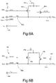
- the logic-combination stage 29 comprises six MOS transistors, namely: a first pair of input transistors, of a NMOS type, connected in parallel, and a second pair of input transistors, of a PMOS type, connected in series, which are designed to jointly implement the operation of OR logic combination of the pre-decoded address signals to be combined psxhvn and sxyhv received at the input; and a pair of output transistors, designed to supply on an output out the decoded address signal DAS HV according to the result of the aforesaid OR logic combination.
- a first NMOS transistor 32a is connected between a first reference line 33, set at a first reference potential, for example equal to the reference voltage V ref , and an internal node 34, and receives on a respective control terminal a respective first negated pre-decoded address signal psxhvn
- a second NMOS transistor 32b is connected between the first reference line 33 and the internal node 34, and receives on the respective control terminal a respective second pre-decoded address signal sxyhv.
- a first PMOS transistor 32c and a second PMOS transistor 32d are connected in series between the internal node 34 and a second reference line 35, set at a second reference potential, for example equal to the boosted voltage V x , and receive on a respective control terminal the second pre-decoded address signal sxyhv and the first negated pre-decoded address signal psxhvn, respectively.
- a pull-up PMOS transistor 32e is connected between the second reference line 35 and the output out, and has its control terminal connected to the internal node 34
- a pull-down PMOS transistor 32f is connected between the first reference line 33 and the same output out, and has its control terminal that is also connected to the internal node 34.
- logic-combination stage 29 implements the following truth table in the OR logic combination of the pre-decoded address signals to be combined sxyhv and psxhvn: sxyhv psxhvn DAS HV 1 1 1 1 0 1 0 1 1 1 0 0 0 0
- the internal node 34 is set at the reference potential (given the closed state of one or both of the NMOS transistors 32a, 32b of the first pair). Consequently, the pull-up PMOS transistor 32e is closed, and the output out goes to the high value (boosted voltage V x ).
- the internal node 34 is set at the high value (boosted voltage V x ), given the closed state of both of the PMOS transistors 32c, 32d of the second pair. Consequently, the pull-down PMOS transistor 32f is closed and the output out goes to the low value (reference voltage V ref ).
- the present Applicant has realized that the row-decoding solution described previously has some limitations, in particular associated to a high occupation of area, which may prove important in applications where size reduction is required (for example, in portable applications).
- US 6,111,792 A discloses a non-volatile semiconductor memory device comprising a mode signal output means for outputting a mode signal for conducting flash programming or flash erasing, a group selection signal output means for outputting a group selection signal for selecting a row decoding group, a first selection means for selecting the row decoding group controlling the word line in accordance with the group selection signal, and a second selection means selecting the word line corresponding to the memory cell from a plurality of the word lines controlled by the row decoding group selected by the first selection means.
- the time required for the flash programming and the flash erasing can be reduced without the addition of a further element and the chip areas can be reduced.
- the aim of the present invention is to overcome, at least in part, the problem highlighted previously in order to provide a row-decoding solution that will be more compact and will have a smaller area occupation.
- a row decoder and a corresponding non-volatile memory device are provided, as defined in the annexed claims.
- the present Applicant has realized that the decoding module and the corresponding plurality of logic-combination stages, one for each wordline WL to be addressed (see the foregoing discussion and Figures 3 and 4 ) represent an important contribution to the total area occupation of the row decoder.
- One aspect of the present solution thus envisages a dedicated implementation (a so-called "custom" implementation) for the logic-combination stages of the decoding module, aimed at reducing area occupation of the row decoder.
- Each logic-combination stage thus implements the truth table referred to above: sxyhv psxhvn DAS HV 1 1 1 1 0 1 0 1 1 1 0 0 0 0
- each of the logic-combination stages has three signal inputs, which are designed to receive: one between a first and a second predecoded address signal to be combined psxhvn, sxyhv, and its negated version; and the other between a first and a second predecoded address signal to be combined psxhvn, sxyhv, or its negated version.
- the logic-combination stages are configured to have an occupation of area halved as compared to traditional solutions, comprising in fact three MOS transistors (as opposed to six of the traditional solutions), of which:
- the row decoder here designated by 38, comprises, in a way substantially similar to what has been discussed previously:
- the decoding module designated herein by 40, arranged between the booster module 14 and the driving module 18, comprises a plurality of logic-combination stages 42, each having: a first input 42a that receives a respective first pre-decoded address signal psxhv from the first booster stages 26; a second input 42b that receives a respective second pre-decoded address signal sxyhv from the second booster stages 27; a third input 42c that receives the second negated pre-decoded address signal sxyhvn (generated as discussed hereinafter); and an output out that supplies a respective decoded address signal DAS HV .
- the negated version (psxhvn) of the first pre-decoded address signal psxhv constitutes the first predecoded address signal to be combined
- the second pre-decoded address signal sxyhv constitutes the second predecoded address signal to be combined by the logic-combination stage 42.
- Each logic-combination stage 42 further has a fourth input 42d, designed to receive the reference voltage V ref , and a fifth input 42e designed to receive the boosted voltage V x .
- the decoding module 40 comprises in this case a plurality of first buffer stages 44 (in the example, sixty-four in number) operating as inverters, each receiving a second pre-decoded address signal sxyhv from the second booster stages 27, and supplying at output the negated version of the same second pre-decoded address signal: sxyhvn. Instead, in this case no buffer stages at output from the first booster stages 26 are present.
- the bulk terminal of the pass transistor 45a is biased at the reference voltage V ref (being coupled to the fourth input 42d), whereas the bulk terminal of the pull-up transistors 46a, 46b is biased at the boosted voltage V x (being coupled to the fifth input 42e).
- circuit embodiment described is such as not to enable setting-up of a direct conduction path (which is potentially destructive) between the line set at the boosted voltage V x and the line set at the reference potential V ref .
- the decoding module 40 further comprises a plurality of second buffer stages 46 (in the example, a hundred and twenty-eight), each receiving a first pre-decoded address signal psxhv from the first booster stages 26, and supplying at the output the negated version of the same first pre-decoded address signal, psxhvn.
- Each logic-combination stage 42 has in this case: a first input 42a that receives a respective second negated pre-decoded address signal sxyhvn from the first buffer stages 44; a second input 42b that receives a respective first negated pre-decoded address signal psxhvn from the second buffer stages 46; and a third input 42c that receives the respective first pre-decoded address signal psxhv from the first booster stages 26.
- a corresponding second embodiment for the logic-combination stage 42 envisages in this case that:
- this circuit configuration enables implementation of the desired truth table for the OR logic combination of the high predecoded address signals to be combined psxhvn, sxyhv, and in particular that:
- the decoding module 40 again comprises both the first and the second buffer stages 44, 46.
- Each logic-combination stage 42 has in this case: a first input 42a that receives a respective second negated pre-decoded address signal sxyhvn from the first buffer stages 44; a second input 42b that receives a first negated pre-decoded address signal psxhvn from the second buffer stages 46; and a third input 42c that receives the respective second pre-decoded address signal sxyhv from the second booster stages 27.
- the logic-combination stage 42 in a corresponding third embodiment comprises:
- the decoding module 40 only comprises the second buffer stages 46 (the first buffer stages 44 in this case are not present) .
- Each logic-combination stage 42 has in this case: a first input 42a that receives a respective first pre-decoded address signal psxhv from the first booster stages 26; a second input 42b that receives a respective second pre-decoded address signal sxyhv from the second booster stages 27; and a third input 42c that receives the respective first negated pre-decoded address signal psxhvn from the second buffer stages 46.
- a corresponding fourth embodiment of the logic-combination stage 42 is substantially similar to the third embodiment illustrated with reference to Figure 6c , and thus comprises:
- the solution proposed enables reduction of the occupation of area of the row decoder 38 in a non-volatile memory device, in particular of a flash type.
- the present Applicant has realized that, given the same performance as compared to known solutions (for example, the solution described with reference to Figures 2 and 3 ), it is possible to obtain a reduction of area of around 20% for the entire row decoder 38.
- removal of the first buffer stage 44 or the second buffer stage 46 may contribute to the total reduction of area, at least in some embodiments; this removal may be accompanied, however, by an increase in the area of the first or second booster stages 26, 27 (in particular, of the corresponding output portion, principally for reasons of fan-out, as will be evident to a person skilled in the field).
- the present Applicant further has realized that, given the same area as compared to traditional embodiments, the present solution alternatively enables an increase to be obtained in the speed of the decoding operations performed by the row decoder 38 of around 30% of the total decoding time.
- the aforesaid increase in speed may be achieved principally via increase of the area of the transistors of the inverters 30 in the driving module 18 of the row decoder 38 (this increase in turn being allowed by the aforementioned reduction of the area of the logic-combination stages 42).
- non-volatile memory devices for example, embedded or stand-alone flash devices
- a reduced occupation of area is required.
Landscapes
- Engineering & Computer Science (AREA)
- Microelectronics & Electronic Packaging (AREA)
- Read Only Memory (AREA)
- Dram (AREA)
Claims (8)
- Décodeur de ligne (38), pour un dispositif de mémoire non volatile (1) pourvu d'une matrice mémoire (2) comportant des cellules de mémoire (3) disposées en une pluralité de lignes de mots (WL), comprenant :un module d'entrée et de prédécodage (10, 12, 14), configuré pour recevoir des signaux d'adresse (ASr) et pour générer des signaux d'adresse prédécodés (PASHV) ;un module de décodage (40), configuré pour recevoir lesdits signaux d'adresse prédécodés (PASHV), pour générer des signaux d'adresse décodés (DASHV), ayant une valeur haute ou basse selon l'opération de décodage ; etun module de pilotage (18), configuré pour générer des signaux de polarisation (S_WL) pour la polarisation des lignes de mots (WL) de ladite matrice mémoire (2) à partir desdits signaux d'adresse décodés (DASHV),caractérisé en ce que ledit module de décodage (40) comporte une pluralité d'étages de décodage (42), chacun d'entre eux étant conçu pour réaliser une opération de combinaison logique OU entre un premier signal d'adresse prédécodé (psxhvn) et un deuxième signal d'adresse prédécodé (sxyhv) à combiner pour générer un signal d'adresse décodé respectif (DASHV)sur une sortie respective (out), et chacun d'entre eux ne comprenant que trois transistors, qui comprennent :- au moins un premier transistor de passage (45a), conçu pour transférer sélectivement sur la sortie (out) la valeur d'un signal parmi les premier et deuxième signaux d'adresse prédécodés à combiner (psxhvn, sxyhv), dans au moins une première condition de fonctionnement ;- au moins un premier transistor de rappel vers le niveau haut (46a), conçu pour amener sélectivement la sortie (out) à l'état haut, dans au moins une deuxième condition de fonctionnement ; et- un deuxième transistor de rappel vers le niveau haut (46b) couplé fonctionnellement au premier transistor de rappel vers le niveau haut (46a),dans lequel chaque étage de décodage (42) a une première entrée (42a) conçue pour recevoir ladite version inversée de l'autre signal parmi les premier et deuxième signaux d'adresse prédécodés à combiner (psxhvn, sxyhv), et une deuxième entrée (42b), conçue pour recevoir ledit un signal parmi les premier et deuxième signaux d'adresse prédécodés à combiner (psxhvn, sxyhv) ;dans lequel ledit premier transistor de passage (45a) est connecté entre la deuxième entrée (45b) et la sortie (out) et a sa borne de commande couplée à ladite première entrée (42a) ; ledit premier transistor de rappel vers le niveau haut (46a) est connecté entre ladite sortie (out) et une autre entrée (42e) mise à une tension augmentée (Vx) et a sa borne de commande couplée à ladite première entrée (42a), ledit premier transistor de passage (45a) et ledit premier transistor de rappel vers le niveau haut (46a) étant commandés par la version inversée de l'autre signal parmi les premier et deuxième signaux d'adresse prédécodés à combiner (psxhvn, sxyhv) ; et ledit deuxième transistor de rappel vers le niveau haut (46b) est connecté en parallèle audit premier transistor de rappel vers le niveau haut (46a) entre ladite sortie (out) et ladite autre entrée (42e) et a sa borne de commande couplée à une troisième entrée (42c) dudit étage de décodage (42) conçue pour recevoir la version inversée dudit un signal parmi les premier et deuxième signaux d'adresse prédécodés à combiner (psxhvn, sxyhv).
- Décodeur de ligne (38), pour un dispositif de mémoire non volatile (1) pourvu d'une matrice mémoire (2) comportant des cellules de mémoire (3) disposées en une pluralité de lignes de mots (WL), comprenant :un module d'entrée et de prédécodage (10, 12, 14), configuré pour recevoir des signaux d'adresse (ASr) et pour générer des signaux d'adresse prédécodés (PASHV) ;un module de décodage (40), configuré pour recevoir lesdits signaux d'adresse prédécodés (PASHV), pour générer des signaux d'adresse décodés (DASHV), ayant une valeur haute ou basse selon l'opération de décodage ; etun module de pilotage (18), configuré pour générer des signaux de polarisation (S_WL) pour la polarisation des lignes de mots (WL) de ladite matrice mémoire (2) à partir desdits signaux d'adresse décodés (DASHV),caractérisé en ce que ledit module de décodage (40) comporte une pluralité d'étages de décodage (42), chacun d'entre eux étant conçu pour réaliser une opération de combinaison logique OU entre un premier signal d'adresse prédécodé (psxhvn) et un deuxième signal d'adresse prédécodé (sxyhv) à combiner pour générer un signal d'adresse décodé respectif (DASHV) sur une sortie respective (out), et chacun d'entre eux ne comprenant que trois transistors, qui comprennent :- au moins un premier transistor de passage (45a), conçu pour transférer sélectivement sur la sortie (out) la valeur d'un signal parmi les premier et deuxième signaux d'adresse prédécodés à combiner (psxhvn, sxyhv), dans au moins une première condition de fonctionnement ;- au moins un premier transistor de rappel vers le niveau haut (46a), conçu pour amener sélectivement la sortie (out) à l'état haut, dans au moins une deuxième condition de fonctionnement ; et- un deuxième transistor de passage (45b) couplé au premier transistor de passage (45a),dans lequel chaque étage de décodage (42) a une première entrée (42a) conçue pour recevoir ladite version inversée de l'autre signal parmi les premier et deuxième signaux d'adresse prédécodés à combiner (psxhvn, sxyhv), et une deuxième entrée (42b), conçue pour recevoir ledit un signal parmi les premier et deuxième signaux d'adresse prédécodés à combiner (psxhvn, sxyhv) ;dans lequel ledit premier transistor de passage (45a) est connecté entre la deuxième entrée (45b) et la sortie (out) et a sa borne de commande couplée à ladite première entrée (42a) ; ledit premier transistor de rappel vers le niveau haut (46a) est connecté entre ladite sortie (out) et une autre entrée (42e) mise à une tension augmentée (Vx) et a sa borne de commande couplée à ladite première entrée (42a), ledit premier transistor de passage (45a) et ledit premier transistor de rappel vers le niveau haut (46a) étant commandés par la version inversée de l'autre signal parmi les premier et deuxième signaux d'adresse prédécodés à combiner (psxhvn, sxyhv) ; et ledit deuxième transistor de passage (45b) est connecté en parallèle audit premier transistor de passage (45a) entre ladite deuxième entrée (45b) et ladite sortie (out) et a sa borne de commande couplée à une troisième entrée (42c) dudit étage de décodage (42) conçue pour recevoir l'autre signal parmi les premier et deuxième signaux d'adresse prédécodés à combiner (psxhvn, sxyhv).
- Décodeur selon la revendication 1 ou 2, dans lequel ledit premier transistor de passage (45a) est de type NMOS, et ledit premier transistor de rappel vers le niveau haut (46a) est de type PMOS.
- Décodeur selon l'une quelconque des revendications précédentes, dans lequel ledit module de décodage (40) est configuré pour recevoir dudit module d'entrée et de prédécodage (10, 12, 14) la version inversée des premiers signaux d'adresse prédécodés à combiner (psxhv), et les deuxièmes signaux d'adresse prédécodés à combiner (sxyhv), et comprend en outre des premiers étages séparateurs (44) et/ou des deuxièmes étages séparateurs (46), qui sont conçus pour inverser lesdits deuxièmes signaux d'adresse prédécodés à combiner (sxyhv) et/ou ladite version inversée des premiers signaux d'adresse prédécodés à combiner (psxhv) et qui ont des sorties couplées auxdits étages de décodage (42).
- Décodeur selon l'une quelconque des revendications précédentes, dans lequel ledit module d'entrée et de prédécodage (10, 12, 14) comprend :un module d'entrée (10), configuré pour recevoir les signaux d'adresse (ASr) et pour regrouper lesdits signaux d'adresse (ASr) en sous-ensembles pour générer des signaux d'adresse groupés (PASLV) ;un module de prédécodage (12), configuré pour recevoir les signaux d'adresse groupés (PASLV) et pour combiner logiquement lesdits signaux d'adresse groupés (PASLV) pour générer des signaux d'adresse prédécodés à basse tension (
PAS LV) ; etun module d'augmentation (14), configuré pour recevoir lesdits signaux d'adresse prédécodés à basse tension (PAS LV) et pour réaliser une opération d'augmentation de tension pour la génération desdits signaux d'adresse prédécodés (PASHV). - Décodeur selon l'une quelconque des revendications précédentes, dans lequel ledit module de pilotage (18) comprend une pluralité d'unités d'inversion (30), une pour chacune desdites lignes de mots (WL) ; dans lequel chacune desdites unités d'inversion (30) est configurée pour recevoir un signal d'adresse décodé respectif (DASHV) et pour fournir un signal de polarisation respectif (S_WL) pour la ligne de mot respective (WL) de la matrice mémoire (2).
- Dispositif de mémoire non volatile (1) comprenant une matrice mémoire (2) et un décodeur de ligne (20) selon l'une quelconque des revendications précédentes, couplé à la matrice mémoire (2) et conçu pour accéder à et polariser les lignes de mot (WL) de ladite matrice mémoire.
- Dispositif selon la revendication 7, dans lequel ladite matrice mémoire (2) est de type flash NON-ET ou NON-OU.
Applications Claiming Priority (1)
| Application Number | Priority Date | Filing Date | Title |
|---|---|---|---|
| ITUB2015A003728A ITUB20153728A1 (it) | 2015-09-18 | 2015-09-18 | Decodificatore di riga per un dispositivo di memoria non volatile, avente ridotta occupazione di area |
Publications (2)
| Publication Number | Publication Date |
|---|---|
| EP3144937A1 EP3144937A1 (fr) | 2017-03-22 |
| EP3144937B1 true EP3144937B1 (fr) | 2022-05-04 |
Family
ID=55588163
Family Applications (1)
| Application Number | Title | Priority Date | Filing Date |
|---|---|---|---|
| EP16161883.0A Active EP3144937B1 (fr) | 2015-09-18 | 2016-03-23 | Décodeur de rangée pour un dispositif de mémoire non volatile, possédant une zone réduite d'occupation |
Country Status (3)
| Country | Link |
|---|---|
| US (1) | US9767907B2 (fr) |
| EP (1) | EP3144937B1 (fr) |
| IT (1) | ITUB20153728A1 (fr) |
Families Citing this family (3)
| Publication number | Priority date | Publication date | Assignee | Title |
|---|---|---|---|---|
| IT201600098496A1 (it) | 2016-09-30 | 2018-03-30 | St Microelectronics Srl | Decodificatore di indirizzo per una matrice di memoria non volatile utilizzante transistori mos di selezione |
| KR20190070158A (ko) * | 2017-12-12 | 2019-06-20 | 에스케이하이닉스 주식회사 | 어드레스 디코더 및 이를 포함하는 반도체 메모리 장치 |
| KR102526256B1 (ko) * | 2018-03-06 | 2023-04-28 | 에스케이하이닉스 주식회사 | 데이터 출력 버퍼 |
Family Cites Families (7)
| Publication number | Priority date | Publication date | Assignee | Title |
|---|---|---|---|---|
| US5410508A (en) * | 1993-05-14 | 1995-04-25 | Micron Semiconductor, Inc. | Pumped wordlines |
| JP3227698B2 (ja) * | 1998-03-16 | 2001-11-12 | 日本電気株式会社 | 不揮発性半導体記憶装置 |
| US7286439B2 (en) * | 2004-12-30 | 2007-10-23 | Sandisk 3D Llc | Apparatus and method for hierarchical decoding of dense memory arrays using multiple levels of multiple-headed decoders |
| JP5100035B2 (ja) * | 2005-08-02 | 2012-12-19 | ルネサスエレクトロニクス株式会社 | 半導体記憶装置 |
| ITTO20080645A1 (it) * | 2008-08-29 | 2010-02-28 | St Microelectronics Srl | Decodificatore di riga per dispositivi di memoria non volatili, in particolare del tipo a cambiamento di fase |
| US8351264B2 (en) * | 2008-12-19 | 2013-01-08 | Unity Semiconductor Corporation | High voltage switching circuitry for a cross-point array |
| ITTO20120412A1 (it) * | 2012-05-08 | 2013-11-09 | St Microelectronics Srl | Circuito decodificatore di riga per un dispositivo di memoria non volatile a cambiamento di fase |
-
2015
- 2015-09-18 IT ITUB2015A003728A patent/ITUB20153728A1/it unknown
-
2016
- 2016-03-23 EP EP16161883.0A patent/EP3144937B1/fr active Active
- 2016-03-28 US US15/083,056 patent/US9767907B2/en active Active
Also Published As
| Publication number | Publication date |
|---|---|
| EP3144937A1 (fr) | 2017-03-22 |
| US9767907B2 (en) | 2017-09-19 |
| US20170084334A1 (en) | 2017-03-23 |
| ITUB20153728A1 (it) | 2017-03-18 |
Similar Documents
| Publication | Publication Date | Title |
|---|---|---|
| US6560144B2 (en) | Nonvolatile semiconductor memory device | |
| US6535430B2 (en) | Wordline decoder for flash memory | |
| US9966145B2 (en) | Row decoder for a non-volatile memory device, and non-volatile memory device | |
| JP5059199B2 (ja) | Cmosデコーディング回路 | |
| CN108352179B (zh) | 用于减少泄漏的sram架构 | |
| US20020196695A1 (en) | Column multiplexer for semiconductor memories | |
| US6069838A (en) | Semiconductor memory device having sub-word line driving circuit | |
| CN105845178A (zh) | 半导体器件 | |
| KR100274923B1 (ko) | 디램 내장 논리 반도체 집적 회로 장치 | |
| EP3144937B1 (fr) | Décodeur de rangée pour un dispositif de mémoire non volatile, possédant une zone réduite d'occupation | |
| JP3223877B2 (ja) | 半導体記憶装置 | |
| US6111792A (en) | Non-volatile semiconductor memory device for selective cell flash erasing/programming | |
| US20190287610A1 (en) | Memory circuit and electronic device | |
| US7965561B2 (en) | Row selector occupying a reduced device area for semiconductor memory devices | |
| US7639557B1 (en) | Configurable random-access-memory circuitry | |
| US10360333B1 (en) | Configuration memory circuit | |
| EP4339953B1 (fr) | Dispositif de mémoire non volatile et procédé de fonctionnement correspondant | |
| KR20180012910A (ko) | Otp 메모리 장치 | |
| CN107086052B (zh) | 闪速存储器 | |
| US5491658A (en) | Column decoder for virtual ground memory array | |
| KR100399975B1 (ko) | 포지티브 챠지 펌핑 전압 스위칭 회로 및 그를 이용한플래쉬 메모리의 로우 디코더 회로 | |
| KR102365003B1 (ko) | Otp 메모리 장치 | |
| CN117711462A (zh) | 非易失性存储器设备以及对应的操作方法 | |
| US6847579B2 (en) | Semiconductor memory device | |
| US20170179948A1 (en) | Signal transfer circuit and circuit for generating hit signal including the same |
Legal Events
| Date | Code | Title | Description |
|---|---|---|---|
| PUAI | Public reference made under article 153(3) epc to a published international application that has entered the european phase |
Free format text: ORIGINAL CODE: 0009012 |
|
| STAA | Information on the status of an ep patent application or granted ep patent |
Free format text: STATUS: THE APPLICATION HAS BEEN PUBLISHED |
|
| AK | Designated contracting states |
Kind code of ref document: A1 Designated state(s): AL AT BE BG CH CY CZ DE DK EE ES FI FR GB GR HR HU IE IS IT LI LT LU LV MC MK MT NL NO PL PT RO RS SE SI SK SM TR |
|
| AX | Request for extension of the european patent |
Extension state: BA ME |
|
| STAA | Information on the status of an ep patent application or granted ep patent |
Free format text: STATUS: REQUEST FOR EXAMINATION WAS MADE |
|
| 17P | Request for examination filed |
Effective date: 20170920 |
|
| RBV | Designated contracting states (corrected) |
Designated state(s): AL AT BE BG CH CY CZ DE DK EE ES FI FR GB GR HR HU IE IS IT LI LT LU LV MC MK MT NL NO PL PT RO RS SE SI SK SM TR |
|
| STAA | Information on the status of an ep patent application or granted ep patent |
Free format text: STATUS: EXAMINATION IS IN PROGRESS |
|
| 17Q | First examination report despatched |
Effective date: 20200814 |
|
| GRAP | Despatch of communication of intention to grant a patent |
Free format text: ORIGINAL CODE: EPIDOSNIGR1 |
|
| STAA | Information on the status of an ep patent application or granted ep patent |
Free format text: STATUS: GRANT OF PATENT IS INTENDED |
|
| GRAJ | Information related to disapproval of communication of intention to grant by the applicant or resumption of examination proceedings by the epo deleted |
Free format text: ORIGINAL CODE: EPIDOSDIGR1 |
|
| GRAP | Despatch of communication of intention to grant a patent |
Free format text: ORIGINAL CODE: EPIDOSNIGR1 |
|
| INTG | Intention to grant announced |
Effective date: 20211012 |
|
| INTG | Intention to grant announced |
Effective date: 20211027 |
|
| GRAS | Grant fee paid |
Free format text: ORIGINAL CODE: EPIDOSNIGR3 |
|
| GRAA | (expected) grant |
Free format text: ORIGINAL CODE: 0009210 |
|
| STAA | Information on the status of an ep patent application or granted ep patent |
Free format text: STATUS: THE PATENT HAS BEEN GRANTED |
|
| RAP3 | Party data changed (applicant data changed or rights of an application transferred) |
Owner name: STMICROELECTRONICS S.R.L. |
|
| AK | Designated contracting states |
Kind code of ref document: B1 Designated state(s): AL AT BE BG CH CY CZ DE DK EE ES FI FR GB GR HR HU IE IS IT LI LT LU LV MC MK MT NL NO PL PT RO RS SE SI SK SM TR |
|
| REG | Reference to a national code |
Ref country code: GB Ref legal event code: FG4D |
|
| REG | Reference to a national code |
Ref country code: CH Ref legal event code: EP |
|
| REG | Reference to a national code |
Ref country code: AT Ref legal event code: REF Ref document number: 1489977 Country of ref document: AT Kind code of ref document: T Effective date: 20220515 |
|
| REG | Reference to a national code |
Ref country code: DE Ref legal event code: R096 Ref document number: 602016071666 Country of ref document: DE |
|
| REG | Reference to a national code |
Ref country code: IE Ref legal event code: FG4D |
|
| REG | Reference to a national code |
Ref country code: LT Ref legal event code: MG9D |
|
| REG | Reference to a national code |
Ref country code: NL Ref legal event code: MP Effective date: 20220504 |
|
| REG | Reference to a national code |
Ref country code: AT Ref legal event code: MK05 Ref document number: 1489977 Country of ref document: AT Kind code of ref document: T Effective date: 20220504 |
|
| PG25 | Lapsed in a contracting state [announced via postgrant information from national office to epo] |
Ref country code: SE Free format text: LAPSE BECAUSE OF FAILURE TO SUBMIT A TRANSLATION OF THE DESCRIPTION OR TO PAY THE FEE WITHIN THE PRESCRIBED TIME-LIMIT Effective date: 20220504 Ref country code: PT Free format text: LAPSE BECAUSE OF FAILURE TO SUBMIT A TRANSLATION OF THE DESCRIPTION OR TO PAY THE FEE WITHIN THE PRESCRIBED TIME-LIMIT Effective date: 20220905 Ref country code: NO Free format text: LAPSE BECAUSE OF FAILURE TO SUBMIT A TRANSLATION OF THE DESCRIPTION OR TO PAY THE FEE WITHIN THE PRESCRIBED TIME-LIMIT Effective date: 20220804 Ref country code: NL Free format text: LAPSE BECAUSE OF FAILURE TO SUBMIT A TRANSLATION OF THE DESCRIPTION OR TO PAY THE FEE WITHIN THE PRESCRIBED TIME-LIMIT Effective date: 20220504 Ref country code: LT Free format text: LAPSE BECAUSE OF FAILURE TO SUBMIT A TRANSLATION OF THE DESCRIPTION OR TO PAY THE FEE WITHIN THE PRESCRIBED TIME-LIMIT Effective date: 20220504 Ref country code: HR Free format text: LAPSE BECAUSE OF FAILURE TO SUBMIT A TRANSLATION OF THE DESCRIPTION OR TO PAY THE FEE WITHIN THE PRESCRIBED TIME-LIMIT Effective date: 20220504 Ref country code: GR Free format text: LAPSE BECAUSE OF FAILURE TO SUBMIT A TRANSLATION OF THE DESCRIPTION OR TO PAY THE FEE WITHIN THE PRESCRIBED TIME-LIMIT Effective date: 20220805 Ref country code: FI Free format text: LAPSE BECAUSE OF FAILURE TO SUBMIT A TRANSLATION OF THE DESCRIPTION OR TO PAY THE FEE WITHIN THE PRESCRIBED TIME-LIMIT Effective date: 20220504 Ref country code: ES Free format text: LAPSE BECAUSE OF FAILURE TO SUBMIT A TRANSLATION OF THE DESCRIPTION OR TO PAY THE FEE WITHIN THE PRESCRIBED TIME-LIMIT Effective date: 20220504 Ref country code: BG Free format text: LAPSE BECAUSE OF FAILURE TO SUBMIT A TRANSLATION OF THE DESCRIPTION OR TO PAY THE FEE WITHIN THE PRESCRIBED TIME-LIMIT Effective date: 20220804 Ref country code: AT Free format text: LAPSE BECAUSE OF FAILURE TO SUBMIT A TRANSLATION OF THE DESCRIPTION OR TO PAY THE FEE WITHIN THE PRESCRIBED TIME-LIMIT Effective date: 20220504 |
|
| PG25 | Lapsed in a contracting state [announced via postgrant information from national office to epo] |
Ref country code: RS Free format text: LAPSE BECAUSE OF FAILURE TO SUBMIT A TRANSLATION OF THE DESCRIPTION OR TO PAY THE FEE WITHIN THE PRESCRIBED TIME-LIMIT Effective date: 20220504 Ref country code: PL Free format text: LAPSE BECAUSE OF FAILURE TO SUBMIT A TRANSLATION OF THE DESCRIPTION OR TO PAY THE FEE WITHIN THE PRESCRIBED TIME-LIMIT Effective date: 20220504 Ref country code: LV Free format text: LAPSE BECAUSE OF FAILURE TO SUBMIT A TRANSLATION OF THE DESCRIPTION OR TO PAY THE FEE WITHIN THE PRESCRIBED TIME-LIMIT Effective date: 20220504 Ref country code: IS Free format text: LAPSE BECAUSE OF FAILURE TO SUBMIT A TRANSLATION OF THE DESCRIPTION OR TO PAY THE FEE WITHIN THE PRESCRIBED TIME-LIMIT Effective date: 20220904 |
|
| PG25 | Lapsed in a contracting state [announced via postgrant information from national office to epo] |
Ref country code: SM Free format text: LAPSE BECAUSE OF FAILURE TO SUBMIT A TRANSLATION OF THE DESCRIPTION OR TO PAY THE FEE WITHIN THE PRESCRIBED TIME-LIMIT Effective date: 20220504 Ref country code: SK Free format text: LAPSE BECAUSE OF FAILURE TO SUBMIT A TRANSLATION OF THE DESCRIPTION OR TO PAY THE FEE WITHIN THE PRESCRIBED TIME-LIMIT Effective date: 20220504 Ref country code: RO Free format text: LAPSE BECAUSE OF FAILURE TO SUBMIT A TRANSLATION OF THE DESCRIPTION OR TO PAY THE FEE WITHIN THE PRESCRIBED TIME-LIMIT Effective date: 20220504 Ref country code: EE Free format text: LAPSE BECAUSE OF FAILURE TO SUBMIT A TRANSLATION OF THE DESCRIPTION OR TO PAY THE FEE WITHIN THE PRESCRIBED TIME-LIMIT Effective date: 20220504 Ref country code: DK Free format text: LAPSE BECAUSE OF FAILURE TO SUBMIT A TRANSLATION OF THE DESCRIPTION OR TO PAY THE FEE WITHIN THE PRESCRIBED TIME-LIMIT Effective date: 20220504 Ref country code: CZ Free format text: LAPSE BECAUSE OF FAILURE TO SUBMIT A TRANSLATION OF THE DESCRIPTION OR TO PAY THE FEE WITHIN THE PRESCRIBED TIME-LIMIT Effective date: 20220504 |
|
| REG | Reference to a national code |
Ref country code: DE Ref legal event code: R097 Ref document number: 602016071666 Country of ref document: DE |
|
| PLBE | No opposition filed within time limit |
Free format text: ORIGINAL CODE: 0009261 |
|
| STAA | Information on the status of an ep patent application or granted ep patent |
Free format text: STATUS: NO OPPOSITION FILED WITHIN TIME LIMIT |
|
| PG25 | Lapsed in a contracting state [announced via postgrant information from national office to epo] |
Ref country code: AL Free format text: LAPSE BECAUSE OF FAILURE TO SUBMIT A TRANSLATION OF THE DESCRIPTION OR TO PAY THE FEE WITHIN THE PRESCRIBED TIME-LIMIT Effective date: 20220504 |
|
| 26N | No opposition filed |
Effective date: 20230207 |
|
| PG25 | Lapsed in a contracting state [announced via postgrant information from national office to epo] |
Ref country code: SI Free format text: LAPSE BECAUSE OF FAILURE TO SUBMIT A TRANSLATION OF THE DESCRIPTION OR TO PAY THE FEE WITHIN THE PRESCRIBED TIME-LIMIT Effective date: 20220504 |
|
| PG25 | Lapsed in a contracting state [announced via postgrant information from national office to epo] |
Ref country code: MC Free format text: LAPSE BECAUSE OF FAILURE TO SUBMIT A TRANSLATION OF THE DESCRIPTION OR TO PAY THE FEE WITHIN THE PRESCRIBED TIME-LIMIT Effective date: 20220504 |
|
| REG | Reference to a national code |
Ref country code: CH Ref legal event code: PL |
|
| GBPC | Gb: european patent ceased through non-payment of renewal fee |
Effective date: 20230323 |
|
| REG | Reference to a national code |
Ref country code: BE Ref legal event code: MM Effective date: 20230331 |
|
| PG25 | Lapsed in a contracting state [announced via postgrant information from national office to epo] |
Ref country code: LU Free format text: LAPSE BECAUSE OF NON-PAYMENT OF DUE FEES Effective date: 20230323 |
|
| REG | Reference to a national code |
Ref country code: IE Ref legal event code: MM4A |
|
| PG25 | Lapsed in a contracting state [announced via postgrant information from national office to epo] |
Ref country code: GB Free format text: LAPSE BECAUSE OF NON-PAYMENT OF DUE FEES Effective date: 20230323 |
|
| PG25 | Lapsed in a contracting state [announced via postgrant information from national office to epo] |
Ref country code: LI Free format text: LAPSE BECAUSE OF NON-PAYMENT OF DUE FEES Effective date: 20230331 Ref country code: IT Free format text: LAPSE BECAUSE OF FAILURE TO SUBMIT A TRANSLATION OF THE DESCRIPTION OR TO PAY THE FEE WITHIN THE PRESCRIBED TIME-LIMIT Effective date: 20220504 Ref country code: IE Free format text: LAPSE BECAUSE OF NON-PAYMENT OF DUE FEES Effective date: 20230323 Ref country code: GB Free format text: LAPSE BECAUSE OF NON-PAYMENT OF DUE FEES Effective date: 20230323 Ref country code: FR Free format text: LAPSE BECAUSE OF NON-PAYMENT OF DUE FEES Effective date: 20230331 Ref country code: CH Free format text: LAPSE BECAUSE OF NON-PAYMENT OF DUE FEES Effective date: 20230331 |
|
| PG25 | Lapsed in a contracting state [announced via postgrant information from national office to epo] |
Ref country code: BE Free format text: LAPSE BECAUSE OF NON-PAYMENT OF DUE FEES Effective date: 20230331 |
|
| PG25 | Lapsed in a contracting state [announced via postgrant information from national office to epo] |
Ref country code: BG Free format text: LAPSE BECAUSE OF FAILURE TO SUBMIT A TRANSLATION OF THE DESCRIPTION OR TO PAY THE FEE WITHIN THE PRESCRIBED TIME-LIMIT Effective date: 20220504 |
|
| PG25 | Lapsed in a contracting state [announced via postgrant information from national office to epo] |
Ref country code: BG Free format text: LAPSE BECAUSE OF FAILURE TO SUBMIT A TRANSLATION OF THE DESCRIPTION OR TO PAY THE FEE WITHIN THE PRESCRIBED TIME-LIMIT Effective date: 20220504 |
|
| PGFP | Annual fee paid to national office [announced via postgrant information from national office to epo] |
Ref country code: DE Payment date: 20250218 Year of fee payment: 10 |
|
| PG25 | Lapsed in a contracting state [announced via postgrant information from national office to epo] |
Ref country code: CY Free format text: LAPSE BECAUSE OF FAILURE TO SUBMIT A TRANSLATION OF THE DESCRIPTION OR TO PAY THE FEE WITHIN THE PRESCRIBED TIME-LIMIT; INVALID AB INITIO Effective date: 20160323 |
|
| PG25 | Lapsed in a contracting state [announced via postgrant information from national office to epo] |
Ref country code: HU Free format text: LAPSE BECAUSE OF FAILURE TO SUBMIT A TRANSLATION OF THE DESCRIPTION OR TO PAY THE FEE WITHIN THE PRESCRIBED TIME-LIMIT; INVALID AB INITIO Effective date: 20160323 |
|
| PG25 | Lapsed in a contracting state [announced via postgrant information from national office to epo] |
Ref country code: TR Free format text: LAPSE BECAUSE OF FAILURE TO SUBMIT A TRANSLATION OF THE DESCRIPTION OR TO PAY THE FEE WITHIN THE PRESCRIBED TIME-LIMIT Effective date: 20220504 |