EP3144961A1 - Procédé de traitement laser pour découpe de plaquette de semi-conducteur ayant une couche métallique formée sur celle-ci et dispositif de traitement laser - Google Patents
Procédé de traitement laser pour découpe de plaquette de semi-conducteur ayant une couche métallique formée sur celle-ci et dispositif de traitement laser Download PDFInfo
- Publication number
- EP3144961A1 EP3144961A1 EP15793230.2A EP15793230A EP3144961A1 EP 3144961 A1 EP3144961 A1 EP 3144961A1 EP 15793230 A EP15793230 A EP 15793230A EP 3144961 A1 EP3144961 A1 EP 3144961A1
- Authority
- EP
- European Patent Office
- Prior art keywords
- laser
- semiconductor wafer
- metal layer
- laser beam
- laser processing
- Prior art date
- Legal status (The legal status is an assumption and is not a legal conclusion. Google has not performed a legal analysis and makes no representation as to the accuracy of the status listed.)
- Withdrawn
Links
Images



Classifications
-
- H—ELECTRICITY
- H10—SEMICONDUCTOR DEVICES; ELECTRIC SOLID-STATE DEVICES NOT OTHERWISE PROVIDED FOR
- H10P—GENERIC PROCESSES OR APPARATUS FOR THE MANUFACTURE OR TREATMENT OF DEVICES COVERED BY CLASS H10
- H10P52/00—Grinding, lapping or polishing of wafers, substrates or parts of devices
-
- H—ELECTRICITY
- H10—SEMICONDUCTOR DEVICES; ELECTRIC SOLID-STATE DEVICES NOT OTHERWISE PROVIDED FOR
- H10W—GENERIC PACKAGES, INTERCONNECTIONS, CONNECTORS OR OTHER CONSTRUCTIONAL DETAILS OF DEVICES COVERED BY CLASS H10
- H10W46/00—Marks applied to devices, e.g. for alignment or identification
-
- B—PERFORMING OPERATIONS; TRANSPORTING
- B23—MACHINE TOOLS; METAL-WORKING NOT OTHERWISE PROVIDED FOR
- B23K—SOLDERING OR UNSOLDERING; WELDING; CLADDING OR PLATING BY SOLDERING OR WELDING; CUTTING BY APPLYING HEAT LOCALLY, e.g. FLAME CUTTING; WORKING BY LASER BEAM
- B23K26/00—Working by laser beam, e.g. welding, cutting or boring
- B23K26/02—Positioning or observing the workpiece, e.g. with respect to the point of impact; Aligning, aiming or focusing the laser beam
- B23K26/06—Shaping the laser beam, e.g. by masks or multi-focusing
- B23K26/0604—Shaping the laser beam, e.g. by masks or multi-focusing by a combination of beams
- B23K26/0613—Shaping the laser beam, e.g. by masks or multi-focusing by a combination of beams having a common axis
- B23K26/0617—Shaping the laser beam, e.g. by masks or multi-focusing by a combination of beams having a common axis and with spots spaced along the common axis
-
- B—PERFORMING OPERATIONS; TRANSPORTING
- B23—MACHINE TOOLS; METAL-WORKING NOT OTHERWISE PROVIDED FOR
- B23K—SOLDERING OR UNSOLDERING; WELDING; CLADDING OR PLATING BY SOLDERING OR WELDING; CUTTING BY APPLYING HEAT LOCALLY, e.g. FLAME CUTTING; WORKING BY LASER BEAM
- B23K26/00—Working by laser beam, e.g. welding, cutting or boring
- B23K26/50—Working by transmitting the laser beam through or within the workpiece
- B23K26/53—Working by transmitting the laser beam through or within the workpiece for modifying or reforming the material inside the workpiece, e.g. for producing break initiation cracks
-
- H—ELECTRICITY
- H01—ELECTRIC ELEMENTS
- H01S—DEVICES USING THE PROCESS OF LIGHT AMPLIFICATION BY STIMULATED EMISSION OF RADIATION [LASER] TO AMPLIFY OR GENERATE LIGHT; DEVICES USING STIMULATED EMISSION OF ELECTROMAGNETIC RADIATION IN WAVE RANGES OTHER THAN OPTICAL
- H01S3/00—Lasers, i.e. devices using stimulated emission of electromagnetic radiation in the infrared, visible or ultraviolet wave range
- H01S3/10—Controlling the intensity, frequency, phase, polarisation or direction of the emitted radiation, e.g. switching, gating, modulating or demodulating
-
- H—ELECTRICITY
- H10—SEMICONDUCTOR DEVICES; ELECTRIC SOLID-STATE DEVICES NOT OTHERWISE PROVIDED FOR
- H10P—GENERIC PROCESSES OR APPARATUS FOR THE MANUFACTURE OR TREATMENT OF DEVICES COVERED BY CLASS H10
- H10P14/00—Formation of materials, e.g. in the shape of layers or pillars
- H10P14/20—Formation of materials, e.g. in the shape of layers or pillars of semiconductor materials
- H10P14/29—Formation of materials, e.g. in the shape of layers or pillars of semiconductor materials characterised by the substrates
- H10P14/2901—Materials
- H10P14/2902—Materials being Group IVA materials
- H10P14/2904—Silicon carbide
-
- H—ELECTRICITY
- H10—SEMICONDUCTOR DEVICES; ELECTRIC SOLID-STATE DEVICES NOT OTHERWISE PROVIDED FOR
- H10P—GENERIC PROCESSES OR APPARATUS FOR THE MANUFACTURE OR TREATMENT OF DEVICES COVERED BY CLASS H10
- H10P14/00—Formation of materials, e.g. in the shape of layers or pillars
- H10P14/20—Formation of materials, e.g. in the shape of layers or pillars of semiconductor materials
- H10P14/29—Formation of materials, e.g. in the shape of layers or pillars of semiconductor materials characterised by the substrates
- H10P14/2901—Materials
- H10P14/2902—Materials being Group IVA materials
- H10P14/2905—Silicon, silicon germanium or germanium
-
- H—ELECTRICITY
- H10—SEMICONDUCTOR DEVICES; ELECTRIC SOLID-STATE DEVICES NOT OTHERWISE PROVIDED FOR
- H10P—GENERIC PROCESSES OR APPARATUS FOR THE MANUFACTURE OR TREATMENT OF DEVICES COVERED BY CLASS H10
- H10P14/00—Formation of materials, e.g. in the shape of layers or pillars
- H10P14/20—Formation of materials, e.g. in the shape of layers or pillars of semiconductor materials
- H10P14/29—Formation of materials, e.g. in the shape of layers or pillars of semiconductor materials characterised by the substrates
- H10P14/2901—Materials
- H10P14/2907—Materials being Group IIIA-VA materials
- H10P14/2911—Arsenides
-
- H—ELECTRICITY
- H10—SEMICONDUCTOR DEVICES; ELECTRIC SOLID-STATE DEVICES NOT OTHERWISE PROVIDED FOR
- H10P—GENERIC PROCESSES OR APPARATUS FOR THE MANUFACTURE OR TREATMENT OF DEVICES COVERED BY CLASS H10
- H10P14/00—Formation of materials, e.g. in the shape of layers or pillars
- H10P14/20—Formation of materials, e.g. in the shape of layers or pillars of semiconductor materials
- H10P14/29—Formation of materials, e.g. in the shape of layers or pillars of semiconductor materials characterised by the substrates
- H10P14/2901—Materials
- H10P14/2921—Materials being crystalline insulating materials
-
- H—ELECTRICITY
- H10—SEMICONDUCTOR DEVICES; ELECTRIC SOLID-STATE DEVICES NOT OTHERWISE PROVIDED FOR
- H10P—GENERIC PROCESSES OR APPARATUS FOR THE MANUFACTURE OR TREATMENT OF DEVICES COVERED BY CLASS H10
- H10P34/00—Irradiation with electromagnetic or particle radiation of wafers, substrates or parts of devices
- H10P34/40—Irradiation with electromagnetic or particle radiation of wafers, substrates or parts of devices with high-energy radiation
- H10P34/42—Irradiation with electromagnetic or particle radiation of wafers, substrates or parts of devices with high-energy radiation with electromagnetic radiation, e.g. laser annealing
-
- H—ELECTRICITY
- H10—SEMICONDUCTOR DEVICES; ELECTRIC SOLID-STATE DEVICES NOT OTHERWISE PROVIDED FOR
- H10P—GENERIC PROCESSES OR APPARATUS FOR THE MANUFACTURE OR TREATMENT OF DEVICES COVERED BY CLASS H10
- H10P54/00—Cutting or separating of wafers, substrates or parts of devices
-
- H—ELECTRICITY
- H10—SEMICONDUCTOR DEVICES; ELECTRIC SOLID-STATE DEVICES NOT OTHERWISE PROVIDED FOR
- H10P—GENERIC PROCESSES OR APPARATUS FOR THE MANUFACTURE OR TREATMENT OF DEVICES COVERED BY CLASS H10
- H10P72/00—Handling or holding of wafers, substrates or devices during manufacture or treatment thereof
- H10P72/06—Apparatus for monitoring, sorting, marking, testing or measuring
- H10P72/0614—Marking devices
-
- B—PERFORMING OPERATIONS; TRANSPORTING
- B23—MACHINE TOOLS; METAL-WORKING NOT OTHERWISE PROVIDED FOR
- B23K—SOLDERING OR UNSOLDERING; WELDING; CLADDING OR PLATING BY SOLDERING OR WELDING; CUTTING BY APPLYING HEAT LOCALLY, e.g. FLAME CUTTING; WORKING BY LASER BEAM
- B23K2103/00—Materials to be soldered, welded or cut
- B23K2103/16—Composite materials
- B23K2103/166—Multilayered materials
- B23K2103/172—Multilayered materials wherein at least one of the layers is non-metallic
-
- B—PERFORMING OPERATIONS; TRANSPORTING
- B23—MACHINE TOOLS; METAL-WORKING NOT OTHERWISE PROVIDED FOR
- B23K—SOLDERING OR UNSOLDERING; WELDING; CLADDING OR PLATING BY SOLDERING OR WELDING; CUTTING BY APPLYING HEAT LOCALLY, e.g. FLAME CUTTING; WORKING BY LASER BEAM
- B23K2103/00—Materials to be soldered, welded or cut
- B23K2103/50—Inorganic materials other than metals or composite materials
- B23K2103/56—Inorganic materials other than metals or composite materials being semiconducting
-
- H—ELECTRICITY
- H10—SEMICONDUCTOR DEVICES; ELECTRIC SOLID-STATE DEVICES NOT OTHERWISE PROVIDED FOR
- H10P—GENERIC PROCESSES OR APPARATUS FOR THE MANUFACTURE OR TREATMENT OF DEVICES COVERED BY CLASS H10
- H10P72/00—Handling or holding of wafers, substrates or devices during manufacture or treatment thereof
- H10P72/04—Apparatus for manufacture or treatment
- H10P72/0428—Apparatus for mechanical treatment or grinding or cutting
-
- H—ELECTRICITY
- H10—SEMICONDUCTOR DEVICES; ELECTRIC SOLID-STATE DEVICES NOT OTHERWISE PROVIDED FOR
- H10W—GENERIC PACKAGES, INTERCONNECTIONS, CONNECTORS OR OTHER CONSTRUCTIONAL DETAILS OF DEVICES COVERED BY CLASS H10
- H10W46/00—Marks applied to devices, e.g. for alignment or identification
- H10W46/501—Marks applied to devices, e.g. for alignment or identification for use before dicing
- H10W46/503—Located in scribe lines
Definitions
- the present invention relates to a laser processing method and a laser processing apparatus, and more particularly, to a laser processing method of cutting a semiconductor wafer formed with a metal layer using laser, and a laser processing apparatus therefor.
- a laser processing apparatus irradiates a laser beam, which is emitted from a laser oscillator, on an object to be processed using an optical system to perform a laser processing operation, such as marking, exposure, etching, punching, scribing, dicing, etc., on the object by the irradiated laser beam.
- a laser processing operation such as marking, exposure, etching, punching, scribing, dicing, etc.
- a method of forming a focusing point inside the object with a transmittance with respect to the laser beam and generating a crack to process the object is highlighted. For example, when a laser beam with a high output power is focused to form a focusing point inside a semiconductor wafer, a modified area is formed around the focusing point so that the crack is generated from the modified area. In addition, a laser beam is moved along a predetermined processing line of the semiconductor wafer to generate a crack row inside the object, and then the crack is extended to an external surface of the semiconductor wafer naturally or by using an external force so that the semiconductor wafer can be cut.
- One or more exemplary embodiments provide a laser processing apparatus and a laser processing method of cutting a semiconductor wafer formed with a metal layer using a laser beam.
- an object may be easily cut by transmitting plural laser beams proceeding along a coaxial path to cut the object having a metal layer formed on a surface of a semiconductor wafer, focusing the laser beams at a surface of the metal layer that is a boundary with the semiconductor wafer and a position adjacent to the surface of the semiconductor wafer that is a boundary with the metal layer, and forming focusing points respectively.
- the laser processing method can be simpler since it is not necessary to perform a pre-process of coating a protective layer to protect chips and to perform a cleaning process to remove contamination material after the cutting process.
- FIGS. 1 through 4 are diagrams illustrating a general laser processing method of processing a semiconductor wafer 10 formed with a metal layer 20.
- an object 30 to be processed is made of a semiconductor wafer 10 and a metal layer 20 formed on top surface of the semiconductor 10.
- the semiconductor wafer 10 may be a substrate usable in a general semiconductor process and may include Silicon (Si), Silicon Carbide (Sic), Gallium Arsenide (GaAs) or Sappire, for example.
- the semiconductor wafer 10 may include one of various semiconductor materials.
- the metal layer 20 may be a conductive material usable in a general semiconductor process and may include Copper (Cu), Molybdenum (Mo), or Gold (Au), for example.
- the metal layer 20 may include one of various metal components having a high conductivity.
- a laser beam L is focused on the surface of the metal layer 20 to form a focusing point P using laser processing apparatus (not illustrated). Thus, a groove may be formed around the focusing point P of the surface of the metal layer 20 due to laser ablation.
- a blade 70 is located on the groove line 50 and then is moved along the groove line 50 to perform a sawing operation such that the object 30 splits into a plurality of chips 30' and 30" as illustrated in FIG. 4 .
- the above-described laser processing method forms the groove line 50 using the laser beam L and then cuts the object 30 using a mechanical apparatus, such as the blade 70.
- this laser processing method needs a pre-coating process on a protection layer (not illustrated) to protect the chips 30' and 30".
- an additional cleaning process is required to remove contamination materials after the cutting operation. Therefore, it has a problem that the laser processing method becomes complicated.
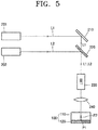
- FIG. 5 is a block diagram illustrating a laser processing apparatus according to an example embodiment of the present invention.
- a laser processing apparatus may include a plurality of laser light sources 201 and 202 to emit a plurality of laser beams L1 and L2, and an optical system to control the plurality of laser beams L1 and L2 to pass through a coaxial path to be incident on an object to be processed, more specifically, a semiconductor wafer 110.
- the object 100 includes the semiconductor wafer 110 and a metal layer 120 formed on one surface of the semiconductor wafer 110 (that is, a lower surface of the semiconductor wafer 110 in FIG. 5 ).
- the semiconductor wafer 110 may be a substrate usable in a general semiconductor process and may include Silicon (Si), Silicon Carbide (Sic), Gallium Arsenide (GaAs) or Sappire, for example.
- the semiconductor wafer 10 may include one of various semiconductor materials.
- the metal layer 20 may be a conductive material usable in a general semiconductor process and may include Copper (Cu), Molybdenum (Mo), or Gold (Au), for example.
- the metal layer 20 may include one of various metal components having a high conductivity.
- the plurality of laser light sources 201 and 202 may include a first laser light source 201 to emit a first laser beam L1 of a pulse type and a second laser light source 202 to emit a second laser beam L2 of a pulse type.
- the first and second laser beams L1 and L2 may have a wavelength between about 900 nm to about 1700 nm, however, the present invention is not limited thereto.
- the first laser beam L1 forms a first focusing point P1 on the surface of the metal layer 120 that is a boundary with the semiconductor wafer 110, as described later.
- the second laser beam L2 forms a second focusing point P2 at a position disposed adjacent to the surface of the semiconductor wafer 110 (the lower surface of the semiconductor in FIG.
- the first laser beam L1 may have a pulse width smaller than the second laser beam L2.
- the first laser beam L1 may have a pulse width of a range of femto seconds (fs)
- the second laser beam L2 may have a pulse width of a range of nano seconds (ns).
- the first laser beam L1 may have a pulse width in a range between about 50 to 200 fs
- the second laser beam L2 may have a pulse width in a range between about 300 to 800 ns.
- the present invention is not limited thereto.
- the first and second laser beams L1 and L2 may have different pulse widths.
- the first laser beam L1 emitted from the first laser light source 201 may proceed along a predetermined path, be reflected by a mirror 210, transmit a beam splitter 220, and then be incident on a beam expansion unit 230.
- an additional optical unit for example, a half-wave plate, a polarization beam splitter (PBS), etc., may be provided on an optical path between the first laser light source 201 and the mirror 210 if necessary.
- the second laser beam L2 emitted from the second laser light source 202 may proceed along a predetermined path, be reflected by the beam splitter 220, and then be incident on the beam expansion unit 230.
- an additional optical unit may be provided on an optical path between the second laser light source 202 and the beam splitter 220 if necessary.
- the first and second laser beams L1 and L2 emitted from the beam splitter 220 pass through the beam expansion unit 230 and a condenser lens 240, transmit the semiconductor wafer 110, and then are focused to form first and second focusing points P1 and P2, respectively.
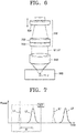
- FIG. 6 illustrates details of the beam expansion unit 230 and the condenser lens 240 of FIG. 5 .
- the beam expansion unit 230 may include a plurality of lenses 231, 232, and 233, and locations of the focusing points P1 and P2 may be changed according to distances among the lenses 231, 232, and 233. Accordingly, the first and second laser beams L1 and L2 incident on the beam expansion unit 230 may be controlled by the beam expansion unit 230 to adjust the locations of the first and second focusing points P1 and P2 formed inside the object 100.
- the first laser beam L1 emitted from the first laser light source 201 is reflected by the mirror 210 to be transmitted to the beam splitter 220, and the second laser beam L2 emitted from the second laser light source 202 is reflected by the beam splitter 220.
- the first and second laser beams L1 and L2 having passed through the beam splitter 220 proceed along a coaxial path.
- the first and second laser beams L1 and L2 having passed along the coaxial path pass through the beam expansion unit 230 and the condenser lens 240 to be focused at predetermined locations in the object 100 to form the first and second focusing points P1 and P2, respectively.
- the locations of the focusing points P1 and P2 may be controlled according to distances among the lenses 231, 232, and 233 of the beam expansion unit 230.
- FIG. 7 is a view illustrating waveforms of the first laser beam L1 and the second laser beam L2, which are emitted from the laser processing apparatus of FIG. 5 , incident on the object 10 with respect to a time axis.
- a set of the first and second laser beams L1 and L2 having a predetermined time difference ⁇ t may be focused inside the object 100 so that the first and second focusing points P1 and P2 can be formed, and then after the object 100 moves by a predetermined distance, a next set of the first and second laser beams L1 and L2 are incident inside the object 100 so that the first and second focusing points P1 and P2 can be moved.
- FIG. 8A illustrates a case in which the first and second focusing points P1 and P2 are formed inside the object 100 by the first and second laser beams L1 and L2 emitted from the laser processing apparatus
- FIG. 8B is a side view of FIG. 8A .
- the object 100 is prepared.
- the object 100 is made of the semiconductor wafer 110 and the metal layer 120 formed on a lower surface of the semiconductor wafer 110.
- the semiconductor wafer 110 and the metal layer 120 may include material usable in the semiconductor manufacturing process as described above.
- the first and second laser beams L1 and L2 of a pulse type having passed the condenser lens 240 of the laser processing apparatus of FIG. 5 are transmitted to an inside of the semiconductor wafer 110 to form the first and second focusing points P1 and P2, respectively.
- the first and second laser beams L1 and L2 are incident on an upper surface of the semiconductor wafer 110 where the metal layer 120 is not formed and transmit the semiconductor wafer 110.
- the first and second laser beams L1 and L2 emitted from the laser processing apparatus proceed along the coaxial path to be incident on the semiconductor wafer 110 as stated above.
- the first and second laser beams L1 and L2 may have a wavelength in a range, for example, about 900 nm to about 1700 nm, however, the present invention is not limited thereto.
- the first laser beam L1 may have a pulse width smaller than the second laser beam L2.
- the first laser beam L1 may have a pulse width of a femto second range (for example, about 50 to 200 fs), and the second laser beam L2 may have a pulse width of a nano second range (for example, about 300 to 800 ns).
- the present invention is not limited thereto, and thus the first and second laser beams L1 and L2 may have different pulse widths than the above-described pulse widths.
- the first and second laser beams L1 and L2 are incident on the transmittable semiconductor wafer 110 with a time difference to form the first and second focusing points P1 and P2, respectively.
- a predetermined time ⁇ t is passed after the first laser beam L1 is incident on the semiconductor wafer 110 to form the first focusing point P1
- the second laser beam L2 is incident on the semiconductor wafer 110 to form the second focusing point P2. Therefore, a set of the first and second laser beams L1 and L2 are incident on the semiconductor wafer 110 with a time difference such that the first and second focusing points P1 and P2 are respectively formed at predetermined positions inside the object 100.
- the first focusing point P1 is formed when the first laser beam L1 transmits the semiconductor wafer 110 and then is focused at a surface of the metal layer 120 which forms a boundary with the semiconductor wafer 110. Therefore, when the first focusing point P1 is formed on the surface of the metal layer 120, a groove can be formed on the surface of the metal layer 120 due to laser ablation. And, the second focusing point P2 is formed when the second laser beam L2 proceeding along the coaxial path with the first laser beam L2 transmits the semiconductor wafer 110 and is focused at a portion disposed adjacent to the lower surface of the semiconductor wafer 110 which forms the boundary with the metal layer 120.
- the second focusing point P2 when the second focusing point P2 is formed at the position adjacent to the lower surface of the semiconductor wafer 110, a modified area is formed around the second focusing point P2 such that a crack can be formed and expanded from the modified area to a surface of the semiconductor wafer 110.
- the second focusing point P2 may be formed at a higher position than the first focusing point P1, and thus the second focusing point P2 may be formed without interference with the groove generated due to the formation of the first focusing point P1.
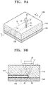
- FIG. 9A illustrates a moving state of the first and second focusing points P1 and P2 after the first and second focusing points P1 and P2 are formed inside the object 100.
- FIG. 9B is a cross-sectional view of a line I-I' of FIG. 9A .
- the object 100 is moved along a predetermined processing line S, and then another set of the first and second laser beams L1 and L2 are incident on the object 100 with the time difference ⁇ t. Accordingly, the first and second focusing points P1 and P2 are formed whiling moving along a predetermined direction (that is, an opposition direction to the movement of the object 100). Meanwhile, the movements of the first and second focusing points P1 and P2 may be performed by movement of the laser processing apparatus instead of the object 100.
- the first and second laser beams L1 and L2 are repeatedly incident inside the object 100 while the object 100 is moved as described above, the first and second focusing points P1 and P2 are moved along the predetermined processing line S inside the object 100.
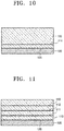
- the internal groove line 125 and the crack row 111 are formed in the object 100, and then, the second laser beam L2 is focused inside the semiconductor wafer 110 to form another focusing point such that at least one internal crack row 112 and 113 is formed additionally by moving the object 100.
- the internal crack rows 112 and 113 can be simultaneously formed by using one or more additional laser beams (not illustrated) when the internal groove line 125 and the crack row are formed.
- the object 100 can be more easily cut according to the one or more internal crack rows 112 and 113.
- the internal groove line 125 can be formed deeper than a single process.
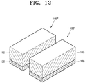
- the object 100 in a state in which the internal groove line 125 and the crack row 111 (and internal crack rows 112 and 113) are formed along the predetermined processing line S inside the object 100 as illustrated in FIG. 11 , the object 100 can be split into a plurality of chips 100' and 100" by breaking naturally or according to an external impact on the object 100.
- an object 100 may be easily cut by transmitting the plural laser beams L1 and L2 proceeding along the coaxial path to cut the object 100 having the metal layer 120 formed on the surface of the semiconductor wafer 110, focusing the laser beams L1 and L2 at the surface of the metal layer 120 that is the boundary with the semiconductor wafer 110 and the position adjacent to the surface of the semiconductor wafer 110 that is the boundary with the metal layer 120, and forming the first and second focusing points P1 and P2, respectively.
- the laser processing method can be simpler since it is not necessary to perform a pre-process of coating a protective layer to protect the chips 100' and 100" and to perform a cleaning process to remove contamination material after the cutting process.
- a laser processing method of processing an object including a semiconductor wafer and a metal layer formed on one surface of the semiconductor wafer by using laser includes passing a plurality of laser beams proceeding along a coaxial path through the semiconductor wafer, and forming focusing points at a surface of the metal layer which forms a boundary with the semiconductor wafer, and at a position disposed adjacent to the surface of the semiconductor wafer, respectively.
- the plurality of laser beams may include first and second laser beams of a pulse type, and the method may further include forming a first focusing point on the surface of the metal layer which forms the boundary with the semiconductor layer, by the first laser beam and forming a second focusing point at the position disposed adjacent to the surface of the semiconductor wafer which forms a boundary with the metal layer, by the second laser beam.
- the second laser beam may be incident on the semiconductor wafer according to a predetermined time lag from the first laser beam.
- the first laser beam and the second laser beam may interfere each other or may not interfere each other.
- the first laser beam may have a smaller pulse width than the second laser beam.
- the first laser beam may have a pulse width of a femto second range
- the second laser beam may have a pulse width of a nano second range.
- the method may further include moving the first focusing point and the second focusing point along predetermined processing line of the object.
- An internal groove line may be formed on the surface of the metal layer according to a movement of the first focusing point, and a crack row may be formed on the position disposed adjacent to the surface of the semiconductor according to a movement of the second focusing point.
- the plurality of laser beams may be incident on the other surface of the semiconductor which is not formed with the metal layer.
- the plurality of laser beams may have wavelengths in a range between 900 nm to about 1700 nm.
- the semiconductor wafer may include Si, Sic, GaAs, or sapphire; and the metal layer may include Cu, Mo, or Au.
- the plurality of laser sources may include a first laser source to emit a first laser beam of a pulse type to form a first focusing point on the surface of the metal layer, and a second laser source to emit a second laser beam of the pulse type to form a second focusing point on the position disposed adjacent to the surface of the semiconductor wafer.
Landscapes
- Physics & Mathematics (AREA)
- Optics & Photonics (AREA)
- Engineering & Computer Science (AREA)
- Plasma & Fusion (AREA)
- Electromagnetism (AREA)
- Mechanical Engineering (AREA)
- Chemical & Material Sciences (AREA)
- Chemical Kinetics & Catalysis (AREA)
- General Chemical & Material Sciences (AREA)
- Oil, Petroleum & Natural Gas (AREA)
- Laser Beam Processing (AREA)
- Dicing (AREA)
- Crystallography & Structural Chemistry (AREA)
Applications Claiming Priority (2)
| Application Number | Priority Date | Filing Date | Title |
|---|---|---|---|
| KR1020140057964A KR20150130835A (ko) | 2014-05-14 | 2014-05-14 | 금속층이 형성된 반도체 웨이퍼를 절단하는 레이저 가공 방법 및 레이저 가공 장치 |
| PCT/KR2015/003696 WO2015174642A1 (fr) | 2014-05-14 | 2015-04-14 | Procédé de traitement laser pour découpe de plaquette de semi-conducteur ayant une couche métallique formée sur celle-ci et dispositif de traitement laser |
Publications (2)
| Publication Number | Publication Date |
|---|---|
| EP3144961A1 true EP3144961A1 (fr) | 2017-03-22 |
| EP3144961A4 EP3144961A4 (fr) | 2018-02-28 |
Family
ID=54480148
Family Applications (1)
| Application Number | Title | Priority Date | Filing Date |
|---|---|---|---|
| EP15793230.2A Withdrawn EP3144961A4 (fr) | 2014-05-14 | 2015-04-14 | Procédé de traitement laser pour découpe de plaquette de semi-conducteur ayant une couche métallique formée sur celle-ci et dispositif de traitement laser |
Country Status (6)
| Country | Link |
|---|---|
| US (1) | US10134681B2 (fr) |
| EP (1) | EP3144961A4 (fr) |
| KR (1) | KR20150130835A (fr) |
| CN (1) | CN106463372B (fr) |
| TW (1) | TWI625777B (fr) |
| WO (1) | WO2015174642A1 (fr) |
Families Citing this family (8)
| Publication number | Priority date | Publication date | Assignee | Title |
|---|---|---|---|---|
| JP6625928B2 (ja) * | 2016-04-27 | 2019-12-25 | 株式会社ディスコ | レーザー加工装置 |
| CN106964894A (zh) * | 2016-11-03 | 2017-07-21 | 苏州镭明激光科技有限公司 | 一种可变双焦点激光微加工装置 |
| WO2020090893A1 (fr) * | 2018-10-30 | 2020-05-07 | 浜松ホトニクス株式会社 | Procédé de traitement par laser |
| US11289378B2 (en) * | 2019-06-13 | 2022-03-29 | Wolfspeed, Inc. | Methods for dicing semiconductor wafers and semiconductor devices made by the methods |
| JP7326053B2 (ja) * | 2019-07-11 | 2023-08-15 | 株式会社ディスコ | 被加工物の加工方法 |
| CN112935528B (zh) * | 2021-01-29 | 2023-05-23 | 西安工业大学 | 一种针对厚度较大晶圆进行高质量切割的方法和装置 |
| TWI890156B (zh) * | 2023-10-03 | 2025-07-11 | 信咚企業股份有限公司 | 雷射多鏡片組合自動定位結構及其實施方法 |
| CN117340450A (zh) * | 2023-12-06 | 2024-01-05 | 国科大杭州高等研究院 | 晶圆切割系统和方法 |
Family Cites Families (16)
| Publication number | Priority date | Publication date | Assignee | Title |
|---|---|---|---|---|
| AU2003211581A1 (en) * | 2002-03-12 | 2003-09-22 | Hamamatsu Photonics K.K. | Method of cutting processed object |
| JP3825753B2 (ja) | 2003-01-14 | 2006-09-27 | 株式会社東芝 | 半導体装置の製造方法 |
| JP2005138143A (ja) * | 2003-11-06 | 2005-06-02 | Disco Abrasive Syst Ltd | レーザ光線を利用する加工装置 |
| US8093530B2 (en) * | 2004-11-19 | 2012-01-10 | Canon Kabushiki Kaisha | Laser cutting apparatus and laser cutting method |
| JP2007142001A (ja) | 2005-11-16 | 2007-06-07 | Denso Corp | レーザ加工装置およびレーザ加工方法 |
| JP2009200140A (ja) | 2008-02-20 | 2009-09-03 | Disco Abrasive Syst Ltd | 半導体チップの製造方法 |
| JP5340806B2 (ja) * | 2009-05-21 | 2013-11-13 | 株式会社ディスコ | 半導体ウエーハのレーザ加工方法 |
| KR101770836B1 (ko) * | 2009-08-11 | 2017-08-23 | 하마마츠 포토닉스 가부시키가이샤 | 레이저 가공장치 및 레이저 가공방법 |
| JP5860217B2 (ja) * | 2011-03-04 | 2016-02-16 | 株式会社ディスコ | レーザー加工装置 |
| US8673741B2 (en) * | 2011-06-24 | 2014-03-18 | Electro Scientific Industries, Inc | Etching a laser-cut semiconductor before dicing a die attach film (DAF) or other material layer |
| JP2013126682A (ja) * | 2011-11-18 | 2013-06-27 | Hamamatsu Photonics Kk | レーザ加工方法 |
| JP6012186B2 (ja) | 2012-01-31 | 2016-10-25 | 浜松ホトニクス株式会社 | 加工対象物切断方法 |
| JP5946308B2 (ja) | 2012-03-28 | 2016-07-06 | 株式会社ディスコ | ウエーハの分割方法 |
| US9040389B2 (en) * | 2012-10-09 | 2015-05-26 | Infineon Technologies Ag | Singulation processes |
| JP2014082317A (ja) * | 2012-10-16 | 2014-05-08 | Disco Abrasive Syst Ltd | ウエーハの加工方法 |
| US8785234B2 (en) * | 2012-10-31 | 2014-07-22 | Infineon Technologies Ag | Method for manufacturing a plurality of chips |
-
2014
- 2014-05-14 KR KR1020140057964A patent/KR20150130835A/ko not_active Ceased
-
2015
- 2015-04-14 EP EP15793230.2A patent/EP3144961A4/fr not_active Withdrawn
- 2015-04-14 CN CN201580025129.0A patent/CN106463372B/zh active Active
- 2015-04-14 WO PCT/KR2015/003696 patent/WO2015174642A1/fr not_active Ceased
- 2015-04-14 US US15/311,038 patent/US10134681B2/en active Active
- 2015-05-13 TW TW104115139A patent/TWI625777B/zh active
Also Published As
| Publication number | Publication date |
|---|---|
| US20170084546A1 (en) | 2017-03-23 |
| WO2015174642A1 (fr) | 2015-11-19 |
| EP3144961A4 (fr) | 2018-02-28 |
| CN106463372A (zh) | 2017-02-22 |
| US10134681B2 (en) | 2018-11-20 |
| TWI625777B (zh) | 2018-06-01 |
| KR20150130835A (ko) | 2015-11-24 |
| TW201606866A (zh) | 2016-02-16 |
| CN106463372B (zh) | 2020-09-08 |
Similar Documents
| Publication | Publication Date | Title |
|---|---|---|
| US10134681B2 (en) | Laser processing method for cutting semiconductor wafer having metal layer formed thereon and laser processing device | |
| KR102024364B1 (ko) | 플라즈마 에칭을 갖는 하이브리드 멀티-스텝 레이저 스크라이빙 프로세스를 이용한 웨이퍼 다이싱 | |
| KR102316372B1 (ko) | 레이저 가공 방법 | |
| JP6081993B2 (ja) | プラズマエッチングを伴うハイブリッドガルバニックレーザスクライビングプロセスを用いたウェハダイシング | |
| US8609512B2 (en) | Method for laser singulation of chip scale packages on glass substrates | |
| KR101754186B1 (ko) | 취성 재료의 레이저 싱귤레이션을 위한 개선된 방법 및 장치 | |
| TWI605508B (zh) | 用於切割具有厚鈍化聚合物層之晶圓的方法以及設備 | |
| TW525240B (en) | Ultraviolet laser ablative patterning of microstructures in semiconductors | |
| JP6605278B2 (ja) | レーザ加工方法 | |
| JP4354376B2 (ja) | レーザ加工装置 | |
| JP2017056469A (ja) | レーザ加工方法及びレーザ加工装置 | |
| JPWO2012063348A1 (ja) | レーザ加工方法及び装置 | |
| US20190217419A1 (en) | Method of processing workpiece with laser beam | |
| WO2017056769A1 (fr) | Procédé de traitement au laser et dispositif de traitement au laser | |
| EP3908423B1 (fr) | Système et procédé de découpage au laser de structures reliées | |
| US20140106543A1 (en) | Laser processing method for wafer | |
| JP2015207721A (ja) | 半導体デバイスの製造方法および半導体デバイスの製造装置 | |
| US20140014631A1 (en) | Laser processing method | |
| KR102060436B1 (ko) | 금속층이 형성된 반도체 웨이퍼를 절단하는 레이저 가공 방법 및 레이저 가공 장치 | |
| TW201402257A (zh) | 鐳射處理的方法和裝置 |
Legal Events
| Date | Code | Title | Description |
|---|---|---|---|
| STAA | Information on the status of an ep patent application or granted ep patent |
Free format text: STATUS: THE INTERNATIONAL PUBLICATION HAS BEEN MADE |
|
| PUAI | Public reference made under article 153(3) epc to a published international application that has entered the european phase |
Free format text: ORIGINAL CODE: 0009012 |
|
| STAA | Information on the status of an ep patent application or granted ep patent |
Free format text: STATUS: REQUEST FOR EXAMINATION WAS MADE |
|
| 17P | Request for examination filed |
Effective date: 20161101 |
|
| AK | Designated contracting states |
Kind code of ref document: A1 Designated state(s): AL AT BE BG CH CY CZ DE DK EE ES FI FR GB GR HR HU IE IS IT LI LT LU LV MC MK MT NL NO PL PT RO RS SE SI SK SM TR |
|
| AX | Request for extension of the european patent |
Extension state: BA ME |
|
| RIN1 | Information on inventor provided before grant (corrected) |
Inventor name: CHEONG, HOE MIN Inventor name: PARK, SANG YOUNG |
|
| DAV | Request for validation of the european patent (deleted) | ||
| DAX | Request for extension of the european patent (deleted) | ||
| A4 | Supplementary search report drawn up and despatched |
Effective date: 20180131 |
|
| RIC1 | Information provided on ipc code assigned before grant |
Ipc: H01L 21/78 20060101AFI20180125BHEP Ipc: B23K 26/00 20140101ALN20180125BHEP |
|
| STAA | Information on the status of an ep patent application or granted ep patent |
Free format text: STATUS: EXAMINATION IS IN PROGRESS |
|
| 17Q | First examination report despatched |
Effective date: 20180808 |
|
| STAA | Information on the status of an ep patent application or granted ep patent |
Free format text: STATUS: THE APPLICATION HAS BEEN WITHDRAWN |
|
| 18W | Application withdrawn |
Effective date: 20190315 |