EP3144965A1 - Verfahren zur beurteilung eines soi-substrats - Google Patents
Verfahren zur beurteilung eines soi-substrats Download PDFInfo
- Publication number
- EP3144965A1 EP3144965A1 EP15793091.8A EP15793091A EP3144965A1 EP 3144965 A1 EP3144965 A1 EP 3144965A1 EP 15793091 A EP15793091 A EP 15793091A EP 3144965 A1 EP3144965 A1 EP 3144965A1
- Authority
- EP
- European Patent Office
- Prior art keywords
- soi substrate
- interface state
- state density
- resistance
- leakage power
- Prior art date
- Legal status (The legal status is an assumption and is not a legal conclusion. Google has not performed a legal analysis and makes no representation as to the accuracy of the status listed.)
- Granted
Links
Images

Classifications
-
- H—ELECTRICITY
- H10—SEMICONDUCTOR DEVICES; ELECTRIC SOLID-STATE DEVICES NOT OTHERWISE PROVIDED FOR
- H10P—GENERIC PROCESSES OR APPARATUS FOR THE MANUFACTURE OR TREATMENT OF DEVICES COVERED BY CLASS H10
- H10P74/00—Testing or measuring during manufacture or treatment of wafers, substrates or devices
- H10P74/20—Testing or measuring during manufacture or treatment of wafers, substrates or devices characterised by the properties tested or measured, e.g. structural or electrical properties
- H10P74/207—Electrical properties, e.g. testing or measuring of resistance, deep levels or capacitance-voltage characteristics
-
- H—ELECTRICITY
- H10—SEMICONDUCTOR DEVICES; ELECTRIC SOLID-STATE DEVICES NOT OTHERWISE PROVIDED FOR
- H10D—INORGANIC ELECTRIC SEMICONDUCTOR DEVICES
- H10D86/00—Integrated devices formed in or on insulating or conducting substrates, e.g. formed in silicon-on-insulator [SOI] substrates or on stainless steel or glass substrates
-
- H—ELECTRICITY
- H10—SEMICONDUCTOR DEVICES; ELECTRIC SOLID-STATE DEVICES NOT OTHERWISE PROVIDED FOR
- H10D—INORGANIC ELECTRIC SEMICONDUCTOR DEVICES
- H10D86/00—Integrated devices formed in or on insulating or conducting substrates, e.g. formed in silicon-on-insulator [SOI] substrates or on stainless steel or glass substrates
- H10D86/201—Integrated devices formed in or on insulating or conducting substrates, e.g. formed in silicon-on-insulator [SOI] substrates or on stainless steel or glass substrates the substrates comprising an insulating layer on a semiconductor body, e.g. SOI
-
- H—ELECTRICITY
- H10—SEMICONDUCTOR DEVICES; ELECTRIC SOLID-STATE DEVICES NOT OTHERWISE PROVIDED FOR
- H10P—GENERIC PROCESSES OR APPARATUS FOR THE MANUFACTURE OR TREATMENT OF DEVICES COVERED BY CLASS H10
- H10P74/00—Testing or measuring during manufacture or treatment of wafers, substrates or devices
- H10P74/20—Testing or measuring during manufacture or treatment of wafers, substrates or devices characterised by the properties tested or measured, e.g. structural or electrical properties
- H10P74/203—Structural properties, e.g. testing or measuring thicknesses, line widths, warpage, bond strengths or physical defects
-
- H—ELECTRICITY
- H10—SEMICONDUCTOR DEVICES; ELECTRIC SOLID-STATE DEVICES NOT OTHERWISE PROVIDED FOR
- H10P—GENERIC PROCESSES OR APPARATUS FOR THE MANUFACTURE OR TREATMENT OF DEVICES COVERED BY CLASS H10
- H10P90/00—Preparation of wafers not covered by a single main group of this subclass, e.g. wafer reinforcement
- H10P90/19—Preparing inhomogeneous wafers
- H10P90/1904—Preparing vertically inhomogeneous wafers
- H10P90/1906—Preparing SOI wafers
-
- H—ELECTRICITY
- H10—SEMICONDUCTOR DEVICES; ELECTRIC SOLID-STATE DEVICES NOT OTHERWISE PROVIDED FOR
- H10P—GENERIC PROCESSES OR APPARATUS FOR THE MANUFACTURE OR TREATMENT OF DEVICES COVERED BY CLASS H10
- H10P95/00—Generic processes or apparatus for manufacture or treatments not covered by the other groups of this subclass
-
- H—ELECTRICITY
- H10—SEMICONDUCTOR DEVICES; ELECTRIC SOLID-STATE DEVICES NOT OTHERWISE PROVIDED FOR
- H10W—GENERIC PACKAGES, INTERCONNECTIONS, CONNECTORS OR OTHER CONSTRUCTIONAL DETAILS OF DEVICES COVERED BY CLASS H10
- H10W44/00—Electrical arrangements for controlling or matching impedance
- H10W44/20—Electrical arrangements for controlling or matching impedance at high-frequency [HF] or radio frequency [RF]
Definitions
- the present invention relates to an SOI (Silicon On Insulator) substrate that is manufactured by bonding silicon single crystal wafers to each other, and more particularly to an evaluation of an SOI substrate used for producing a radio-frequency device, etc.
- SOI Silicon On Insulator
- an RF (Radio-frequency) device primarily intended for a communication interface has attracted attention and it is considered to rapidly evolve in the future.
- devices with low power consumption have been increasingly adopted.
- using an SOI substrate provides a merit of a reduction in power consumption due to a decrease in leak current.
- SoC System on a Chip
- using an SOI wafer can provide a merit of reducing crosstalk between devices in terms of characteristics of an RF transistor.
- the crosstalk means propagation of an undesired electrical signal between devices, and the signal is propagated through a capacitor between wiring lines of devices or through a wafer, for example.
- the crosstalk is reduced as a resistivity of the wafer is increased, a wafer resistivity of a device forming portion cannot be actually extremely increased.
- a buried oxide film layer (a BOX layer) is present between the SOI layer and the base wafer, the crosstalk can be reduced. Furthermore, since a device is not formed on the base wafer serving as an underlying layer of the BOX layer, a high-resistance base wafer can be used without being subject to limitation of device formation, thereby improving RF characteristics.
- a technology that introduces an intermediate layer (a trap layer) such as a polysilicon layer or a nitride oxide to an interface between a BOX layer and a base wafer, and can obtain an SOI wafer with good radio-frequency characteristics thereby so as not to form a inversion layer (see, e.g., Patent Documents 1 and 2, Non-Patent Document 1).
- an intermediate layer such as a polysilicon layer or a nitride oxide
- substrate resistance can be measured by a method such as a spreading resistance measurement and so on, for example.
- a method such as a spreading resistance measurement and so on, for example.
- the present invention was accomplished in view of the above-described problems. It is an object of the present invention to provide a method for evaluating an SOI substrate suited for a radio-frequency device in a simpler manner as possible without forming a device actually for measuring radio-frequency characteristics.
- the present invention provides a method for evaluating a radio-frequency characteristic of an evaluation target SOI substrate upon application of radio-frequency, comprising the steps of:
- the present invention makes it possible to simply evaluate an SOI substrate whether it is suitable for a radio-frequency device or not without producing an actual device.
- This can be converted to a resistance, which is common as a specification of a wafer, and can be defined by a simple value in terms of the resistance as an indicator.
- the first embodiment involves the first step of previously determining a relationship between an interface state density and a leakage power upon application of radio-frequency by using a measuring SOI substrate.
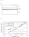
- the measuring SOI substrate to be prepared includes the one same with an evaluation target SOI substrate 5 having an SOI layer 1, a BOX layer 2 of a silicon oxide film, a base wafer 4, and a trap layer 3, which suppresses generation of a carrier at the interface of the BOX layer 2 and the base wafer 4, as shown in FIG. 1 .
- an interface state density of the measuring SOI substrate 5 is measured to determine the interface state density.
- the measurement of the interface state density can be performed by a pseudo MOSFET method using a mercury electrode described in Non-Patent Documents 2 and 3.
- the interface state density can be measured by a CV method described in Non-Patent Document 2 after removing the SOI layer with an alkaline solution.
- radio-frequency is also applied after forming a device, and a leakage power at that time is measured.
- the next step is performed to measure an interface state density of an evaluation target SOI substrate to determine the interface state density.
- the evaluation target SOI substrate is prepared.
- the evaluation target SOI substrate is the SOI substrate 5 having an SOI layer 1, a BOX layer 2, a trap layer 3, and a base wafer 4 as shown in FIG. 1 .
- An interface state density of this evaluation target SOI substrate 5 is measured to determine the interface state density. It is to be noted that the interface state density can be measured by a pseudo MOSFET method using a mercury electrode or a CV method as described above.
- the leakage power of the evaluation target SOI substrate can be estimated and evaluated from the measured interface state density of the evaluation target SOI substrate on the basis of the previously determined relationship between the interface state density and the leakage power on the measuring SOI substrate.
- the present invention makes it possible to evaluate the leakage power, that is radio-frequency characteristics, of an SOI substrate without producing a device actually onto the evaluation target SOI substrate.
- the second embodiment involves the first step of previously determining a relationship between a converted resistance, which is based on a measurement result of an interface state density of a measuring SOI substrate, and a leakage power.
- the interface state density can be converted to the resistance by the following method.
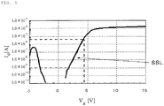
- the value of SSL (Subthreshold Slope) can be determined from the interface state density.
- SSL is defined as voltage (Vg) change when the current (I d ) increases one order of magnitude as shown in FIG. 5 .
- C OX represents a BOX layer capacity
- C Si represents an SOI layer capacity.
- This SSL is defined as a resistance RD (which corresponds to V/I of a resistance component in Equation 2) determined from the interface state density. Then, this resistance RD is converted to an ordinal resistance. The scaling factor in this conversion can be determined previously from the results of radio-frequency measurement (Equations 2 and 3). Incidentally, p represents a resistivity, and R SP represents a spreading resistance.
- radio-frequency is also applied after forming a device, and a leakage power at that time is measured.
- a leakage power of the evaluation target SOI substrate is evaluated on the basis of the previously determined relationship between the resistance and the leakage power.
- the interface state density of the evaluation target SOI substrate is measured, and the obtained interface state density is converted to a resistance in the same manner as described above.
- the leakage power of the evaluation target SOI substrate can be estimated and evaluated from the resistance converted from the interface state density of the evaluation target SOI substrate on the basis of the previously determined relationship between the resistance and the leakage power on the measuring SOI substrate.
- the present invention makes it possible to evaluate the leakage power of an SOI substrate without producing a device actually onto the evaluation target SOI substrate. It is also possible to indicate the substrate characteristics by one criterion of a resistance since the interface state density is converted to the resistance.
- a silicon single crystal wafer doped with boron having a diameter of 200 mm and a resistivity of 1000 ⁇ cm was used as a base wafer.
- 3 ⁇ m of a polycrystalline layer was grown by using trichlorosilane as a raw material gas at 1150°C for a growth time of 3 minutes.
- 0.5 ⁇ m of a polycrystalline layer was grown by using monosilane as a raw material at 570°C for a growth time of 90 minutes to form a trap layer.
- This wafer was bonded with a bond wafer, in which a silicon wafer doped with boron having a diameter of 200 mm and a resistivity of 1000 ⁇ cm had been treated at 1150°C in a Pyro atmosphere for 6 hours to form 1000 nm of an oxide film as a BOX layer, and was subjected to bonding heat treatment. Then, this was reduced the film thickness by polishing to produce an SOI substrate so as to have a 160 nm SOI layer. In the same manner, plural SOI substrates were produced.
- SOI substrates were treated at 450°C in a nitrogen atmosphere containing 1% of hydrogen with varying the annealing time from 5 minutes to 30 minutes to produce plural SOI substrates with the interface state density between the BOX layer and the base wafer being varied.
- each interface state density was measured by a pseudo MOSFET method using a mercury electrode described in Non-Patent Documents 2 and 3.
- each SOI substrate was removed by alkaline etching, and then Al was deposited thereto with a thickness of 2 ⁇ m in order to measure the leakage power. Further, photolithography was performed to form a CPW (Coplanar Waveguides).
- Al electrodes of 150 ⁇ m ⁇ 50 ⁇ m were formed on the measuring SOI substrate so as to have distance of 100 ⁇ m between the electrodes.
- radio-frequency was applied to the measuring SOI substrate with the device formed thereon, and the leakage power between the Al electrodes to the input power was measured.
- the measurement was performed by applying each radio-frequency with a frequency in a range of 1 ⁇ 10 8 to 1 ⁇ 10 11 Hz. From the data of frequency-dependence of the leakage power, values at 1 GHz (1 ⁇ 10 9 Hz), which appeared to clearly reflect the difference of substrates, were adopted as representatives of the leakage power to determine a relationship in FIG. 3 .
- the capacity Csi of the SOI layer with a thickness of 160 nm comes to be 6.53 ⁇ 10 -8 F
- the capacity Cox of the BOX layer with a thickness of 1000 nm comes to be 7.195 ⁇ 10 -8 F. From Equation 1, it was determined that SSL is 0.15 when the interface state density is 1 ⁇ 10 12 cm -2 eV -1 , SSL is 0.015 when the interface state density is 1 ⁇ 10 11 cm -2 eV -1 , and SSL is 0.0015 when the interface state density is 1 ⁇ 10 10 cm -2 eV -1 .
- the SSL was converted to a resistance with the coefficient to convert the SSL into the resistance being set to 10000 in this case on the basis of the relationship with radio-frequency characteristics.
- each converted resistance was determined. Then, the relationship between the converted resistance and the leakage power was determined and shown in FIG. 4 .
- an evaluation target SOI substrate was prepared in the same manner as described above.
- the interface state density was measured by a pseudo MOSFET method. From the measured interface state density, the leakage power of the evaluation target SOI substrate upon application of radio-frequency could be evaluated on the basis of the previously determined relationship between the interface state density and the leakage power in FIG. 3 .
- the converted resistance was determined in the same manner as described above. From the converted resistance, the leakage power of the evaluation target SOI substrate upon application of radio-frequency could be evaluated on the basis of the previously determined relationship between the resistance and the leakage power in FIG. 4 .
Landscapes
- Testing Or Measuring Of Semiconductors Or The Like (AREA)
- Testing Of Individual Semiconductor Devices (AREA)
Applications Claiming Priority (2)
| Application Number | Priority Date | Filing Date | Title |
|---|---|---|---|
| JP2014100758A JP6102823B2 (ja) | 2014-05-14 | 2014-05-14 | Soi基板の評価方法 |
| PCT/JP2015/000943 WO2015173995A1 (ja) | 2014-05-14 | 2015-02-25 | Soi基板の評価方法 |
Publications (3)
| Publication Number | Publication Date |
|---|---|
| EP3144965A1 true EP3144965A1 (de) | 2017-03-22 |
| EP3144965A4 EP3144965A4 (de) | 2018-01-10 |
| EP3144965B1 EP3144965B1 (de) | 2020-11-25 |
Family
ID=54479553
Family Applications (1)
| Application Number | Title | Priority Date | Filing Date |
|---|---|---|---|
| EP15793091.8A Active EP3144965B1 (de) | 2014-05-14 | 2015-02-25 | Verfahren zur beurteilung eines soi-substrats |
Country Status (8)
| Country | Link |
|---|---|
| US (1) | US9780006B2 (de) |
| EP (1) | EP3144965B1 (de) |
| JP (1) | JP6102823B2 (de) |
| KR (1) | KR102185647B1 (de) |
| CN (1) | CN106415806B (de) |
| SG (1) | SG11201608834SA (de) |
| TW (1) | TWI609189B (de) |
| WO (1) | WO2015173995A1 (de) |
Families Citing this family (1)
| Publication number | Priority date | Publication date | Assignee | Title |
|---|---|---|---|---|
| JP6931708B2 (ja) * | 2017-02-10 | 2021-09-08 | グローバルウェーハズ カンパニー リミテッドGlobalWafers Co.,Ltd. | 半導体構造を評価する方法 |
Family Cites Families (13)
| Publication number | Priority date | Publication date | Assignee | Title |
|---|---|---|---|---|
| JPH0233946A (ja) * | 1988-07-23 | 1990-02-05 | Nec Corp | 半導体装置 |
| JP2001060676A (ja) * | 1999-08-20 | 2001-03-06 | Mitsubishi Materials Silicon Corp | 界面準位密度の算出方法 |
| JP4492783B2 (ja) * | 2001-09-12 | 2010-06-30 | 日本電気株式会社 | 半導体装置及びその製造方法 |
| FR2860341B1 (fr) | 2003-09-26 | 2005-12-30 | Soitec Silicon On Insulator | Procede de fabrication de structure multicouche a pertes diminuees |
| WO2005031842A2 (en) | 2003-09-26 | 2005-04-07 | Universite Catholique De Louvain | Method of manufacturing a multilayer semiconductor structure with reduced ohmic losses |
| EP1768173A1 (de) * | 2004-06-25 | 2007-03-28 | Shin-Etsu Handotai Company Limited | Verfahren zum bewerten eines soi-wafers |
| JP4419710B2 (ja) * | 2004-06-25 | 2010-02-24 | 信越半導体株式会社 | Soiウエーハの評価方法 |
| US8225248B2 (en) * | 2005-10-24 | 2012-07-17 | Cadence Design Systems, Inc. | Timing, noise, and power analysis of integrated circuits |
| JP2007324194A (ja) * | 2006-05-30 | 2007-12-13 | Shin Etsu Handotai Co Ltd | Soiウエーハの評価方法 |
| JP4776598B2 (ja) * | 2007-08-23 | 2011-09-21 | 株式会社アドバンテスト | 管理方法、管理装置、及びデバイス製造方法 |
| JP2009231376A (ja) | 2008-03-19 | 2009-10-08 | Shin Etsu Handotai Co Ltd | Soiウェーハ及び半導体デバイスならびにsoiウェーハの製造方法 |
| JP5532680B2 (ja) * | 2009-05-27 | 2014-06-25 | 信越半導体株式会社 | Soiウェーハの製造方法およびsoiウェーハ |
| CN101702627B (zh) * | 2009-10-29 | 2012-10-03 | 华东师范大学 | 一种基于绝缘体上硅工艺的cmos射频开关 |
-
2014
- 2014-05-14 JP JP2014100758A patent/JP6102823B2/ja active Active
-
2015
- 2015-02-25 KR KR1020167030635A patent/KR102185647B1/ko active Active
- 2015-02-25 SG SG11201608834SA patent/SG11201608834SA/en unknown
- 2015-02-25 EP EP15793091.8A patent/EP3144965B1/de active Active
- 2015-02-25 WO PCT/JP2015/000943 patent/WO2015173995A1/ja not_active Ceased
- 2015-02-25 CN CN201580024451.1A patent/CN106415806B/zh active Active
- 2015-02-25 US US15/305,989 patent/US9780006B2/en active Active
- 2015-03-02 TW TW104106446A patent/TWI609189B/zh active
Also Published As
| Publication number | Publication date |
|---|---|
| SG11201608834SA (en) | 2016-11-29 |
| US20170047258A1 (en) | 2017-02-16 |
| WO2015173995A1 (ja) | 2015-11-19 |
| CN106415806A (zh) | 2017-02-15 |
| EP3144965B1 (de) | 2020-11-25 |
| TW201543049A (zh) | 2015-11-16 |
| CN106415806B (zh) | 2019-06-04 |
| JP6102823B2 (ja) | 2017-03-29 |
| EP3144965A4 (de) | 2018-01-10 |
| US9780006B2 (en) | 2017-10-03 |
| JP2015220257A (ja) | 2015-12-07 |
| TWI609189B (zh) | 2017-12-21 |
| KR102185647B1 (ko) | 2020-12-02 |
| KR20170003554A (ko) | 2017-01-09 |
Similar Documents
| Publication | Publication Date | Title |
|---|---|---|
| Dumka et al. | Electrical and thermal performance of AlGaN/GaN HEMTs on diamond substrate for RF applications | |
| EP2075839B1 (de) | Verfahren zum evaluieren eines soi-wafers | |
| JP7209776B2 (ja) | 半導体構造を評価する方法 | |
| US5786231A (en) | Screening method for selecting semiconductor substrates having defects below a predetermined level in an oxide layer | |
| CN102364682B (zh) | 垂直双扩散mos晶体管测试结构及形成方法、测试方法 | |
| Lotfi et al. | LDMOS-transistors on semi-insulating silicon-on-polycrystalline-silicon carbide substrates for improved RF and thermal properties | |
| EP3144965B1 (de) | Verfahren zur beurteilung eines soi-substrats | |
| KR101205115B1 (ko) | 반도체 디바이스 및 그 제조 방법 | |
| US8089274B2 (en) | Method for evaluating SOI wafer | |
| CN109085486A (zh) | 一种半导体-绝缘体界面态密度和俘获截面的测试方法 | |
| Schwarzenbach et al. | Systematic evaluation of SOI buried oxide reliability for partially depleted and fully depleted applications | |
| Lotfi et al. | Fabrication and characterization of 150-mm silicon-on-polycrystalline silicon carbide substrates | |
| JP6031971B2 (ja) | 半導体試料の電気的評価方法および評価装置 | |
| JP5018053B2 (ja) | 半導体ウエーハの評価方法 | |
| Ardaravičius et al. | Estimation of the charged defect density from hot-electron transport studies in epitaxial ZnO | |
| EP1610373A2 (de) | Methode und Vorrichtung zur Bestimmung der Generations-Lebensdauer | |
| Minami et al. | Electrical characterization of wafer-bonded Ge (111)-on-insulator substrates using four-point-probe pseudo-metal-oxide-semiconductor field-effect transistor method | |
| Wang et al. | Investigation of Bending-Induced Degradation of Flexible AlGaN/GaN HEMTs | |
| Karsenty et al. | A comparative study of electrical transport phenomena in ultrathin vs. nanoscale SOI MOSFETs devices | |
| Lin et al. | Electrical characterisation of ion-implanted silicon-on-sapphire | |
| George | MOSCAP Oxide Charges | |
| Karsenty et al. | Research Article Influence of Series Massive Resistance on Capacitance and Conductance Characteristics in Gate-Recessed Nanoscale SOI MOSFETs |
Legal Events
| Date | Code | Title | Description |
|---|---|---|---|
| STAA | Information on the status of an ep patent application or granted ep patent |
Free format text: STATUS: THE INTERNATIONAL PUBLICATION HAS BEEN MADE |
|
| PUAI | Public reference made under article 153(3) epc to a published international application that has entered the european phase |
Free format text: ORIGINAL CODE: 0009012 |
|
| STAA | Information on the status of an ep patent application or granted ep patent |
Free format text: STATUS: REQUEST FOR EXAMINATION WAS MADE |
|
| 17P | Request for examination filed |
Effective date: 20161108 |
|
| AK | Designated contracting states |
Kind code of ref document: A1 Designated state(s): AL AT BE BG CH CY CZ DE DK EE ES FI FR GB GR HR HU IE IS IT LI LT LU LV MC MK MT NL NO PL PT RO RS SE SI SK SM TR |
|
| AX | Request for extension of the european patent |
Extension state: BA ME |
|
| DAX | Request for extension of the european patent (deleted) | ||
| A4 | Supplementary search report drawn up and despatched |
Effective date: 20171212 |
|
| RIC1 | Information provided on ipc code assigned before grant |
Ipc: H01L 27/12 20060101ALI20171206BHEP Ipc: H01L 21/02 20060101ALI20171206BHEP Ipc: H01L 21/66 20060101AFI20171206BHEP |
|
| GRAP | Despatch of communication of intention to grant a patent |
Free format text: ORIGINAL CODE: EPIDOSNIGR1 |
|
| STAA | Information on the status of an ep patent application or granted ep patent |
Free format text: STATUS: GRANT OF PATENT IS INTENDED |
|
| INTG | Intention to grant announced |
Effective date: 20200619 |
|
| RIN1 | Information on inventor provided before grant (corrected) |
Inventor name: OHTSUKI, TSUYOSHI |
|
| GRAS | Grant fee paid |
Free format text: ORIGINAL CODE: EPIDOSNIGR3 |
|
| GRAA | (expected) grant |
Free format text: ORIGINAL CODE: 0009210 |
|
| STAA | Information on the status of an ep patent application or granted ep patent |
Free format text: STATUS: THE PATENT HAS BEEN GRANTED |
|
| AK | Designated contracting states |
Kind code of ref document: B1 Designated state(s): AL AT BE BG CH CY CZ DE DK EE ES FI FR GB GR HR HU IE IS IT LI LT LU LV MC MK MT NL NO PL PT RO RS SE SI SK SM TR |
|
| REG | Reference to a national code |
Ref country code: GB Ref legal event code: FG4D |
|
| REG | Reference to a national code |
Ref country code: CH Ref legal event code: EP |
|
| REG | Reference to a national code |
Ref country code: DE Ref legal event code: R096 Ref document number: 602015062613 Country of ref document: DE |
|
| REG | Reference to a national code |
Ref country code: AT Ref legal event code: REF Ref document number: 1339259 Country of ref document: AT Kind code of ref document: T Effective date: 20201215 |
|
| REG | Reference to a national code |
Ref country code: IE Ref legal event code: FG4D |
|
| REG | Reference to a national code |
Ref country code: AT Ref legal event code: MK05 Ref document number: 1339259 Country of ref document: AT Kind code of ref document: T Effective date: 20201125 |
|
| REG | Reference to a national code |
Ref country code: NL Ref legal event code: MP Effective date: 20201125 |
|
| PG25 | Lapsed in a contracting state [announced via postgrant information from national office to epo] |
Ref country code: FI Free format text: LAPSE BECAUSE OF FAILURE TO SUBMIT A TRANSLATION OF THE DESCRIPTION OR TO PAY THE FEE WITHIN THE PRESCRIBED TIME-LIMIT Effective date: 20201125 Ref country code: PT Free format text: LAPSE BECAUSE OF FAILURE TO SUBMIT A TRANSLATION OF THE DESCRIPTION OR TO PAY THE FEE WITHIN THE PRESCRIBED TIME-LIMIT Effective date: 20210325 Ref country code: RS Free format text: LAPSE BECAUSE OF FAILURE TO SUBMIT A TRANSLATION OF THE DESCRIPTION OR TO PAY THE FEE WITHIN THE PRESCRIBED TIME-LIMIT Effective date: 20201125 Ref country code: NO Free format text: LAPSE BECAUSE OF FAILURE TO SUBMIT A TRANSLATION OF THE DESCRIPTION OR TO PAY THE FEE WITHIN THE PRESCRIBED TIME-LIMIT Effective date: 20210225 Ref country code: GR Free format text: LAPSE BECAUSE OF FAILURE TO SUBMIT A TRANSLATION OF THE DESCRIPTION OR TO PAY THE FEE WITHIN THE PRESCRIBED TIME-LIMIT Effective date: 20210226 |
|
| PG25 | Lapsed in a contracting state [announced via postgrant information from national office to epo] |
Ref country code: BG Free format text: LAPSE BECAUSE OF FAILURE TO SUBMIT A TRANSLATION OF THE DESCRIPTION OR TO PAY THE FEE WITHIN THE PRESCRIBED TIME-LIMIT Effective date: 20210225 Ref country code: AT Free format text: LAPSE BECAUSE OF FAILURE TO SUBMIT A TRANSLATION OF THE DESCRIPTION OR TO PAY THE FEE WITHIN THE PRESCRIBED TIME-LIMIT Effective date: 20201125 Ref country code: LV Free format text: LAPSE BECAUSE OF FAILURE TO SUBMIT A TRANSLATION OF THE DESCRIPTION OR TO PAY THE FEE WITHIN THE PRESCRIBED TIME-LIMIT Effective date: 20201125 Ref country code: IS Free format text: LAPSE BECAUSE OF FAILURE TO SUBMIT A TRANSLATION OF THE DESCRIPTION OR TO PAY THE FEE WITHIN THE PRESCRIBED TIME-LIMIT Effective date: 20210325 Ref country code: PL Free format text: LAPSE BECAUSE OF FAILURE TO SUBMIT A TRANSLATION OF THE DESCRIPTION OR TO PAY THE FEE WITHIN THE PRESCRIBED TIME-LIMIT Effective date: 20201125 Ref country code: SE Free format text: LAPSE BECAUSE OF FAILURE TO SUBMIT A TRANSLATION OF THE DESCRIPTION OR TO PAY THE FEE WITHIN THE PRESCRIBED TIME-LIMIT Effective date: 20201125 |
|
| REG | Reference to a national code |
Ref country code: LT Ref legal event code: MG9D |
|
| PG25 | Lapsed in a contracting state [announced via postgrant information from national office to epo] |
Ref country code: HR Free format text: LAPSE BECAUSE OF FAILURE TO SUBMIT A TRANSLATION OF THE DESCRIPTION OR TO PAY THE FEE WITHIN THE PRESCRIBED TIME-LIMIT Effective date: 20201125 |
|
| PG25 | Lapsed in a contracting state [announced via postgrant information from national office to epo] |
Ref country code: LT Free format text: LAPSE BECAUSE OF FAILURE TO SUBMIT A TRANSLATION OF THE DESCRIPTION OR TO PAY THE FEE WITHIN THE PRESCRIBED TIME-LIMIT Effective date: 20201125 Ref country code: SK Free format text: LAPSE BECAUSE OF FAILURE TO SUBMIT A TRANSLATION OF THE DESCRIPTION OR TO PAY THE FEE WITHIN THE PRESCRIBED TIME-LIMIT Effective date: 20201125 Ref country code: RO Free format text: LAPSE BECAUSE OF FAILURE TO SUBMIT A TRANSLATION OF THE DESCRIPTION OR TO PAY THE FEE WITHIN THE PRESCRIBED TIME-LIMIT Effective date: 20201125 Ref country code: CZ Free format text: LAPSE BECAUSE OF FAILURE TO SUBMIT A TRANSLATION OF THE DESCRIPTION OR TO PAY THE FEE WITHIN THE PRESCRIBED TIME-LIMIT Effective date: 20201125 Ref country code: EE Free format text: LAPSE BECAUSE OF FAILURE TO SUBMIT A TRANSLATION OF THE DESCRIPTION OR TO PAY THE FEE WITHIN THE PRESCRIBED TIME-LIMIT Effective date: 20201125 Ref country code: SM Free format text: LAPSE BECAUSE OF FAILURE TO SUBMIT A TRANSLATION OF THE DESCRIPTION OR TO PAY THE FEE WITHIN THE PRESCRIBED TIME-LIMIT Effective date: 20201125 |
|
| REG | Reference to a national code |
Ref country code: DE Ref legal event code: R097 Ref document number: 602015062613 Country of ref document: DE |
|
| PG25 | Lapsed in a contracting state [announced via postgrant information from national office to epo] |
Ref country code: DK Free format text: LAPSE BECAUSE OF FAILURE TO SUBMIT A TRANSLATION OF THE DESCRIPTION OR TO PAY THE FEE WITHIN THE PRESCRIBED TIME-LIMIT Effective date: 20201125 |
|
| PG25 | Lapsed in a contracting state [announced via postgrant information from national office to epo] |
Ref country code: MC Free format text: LAPSE BECAUSE OF FAILURE TO SUBMIT A TRANSLATION OF THE DESCRIPTION OR TO PAY THE FEE WITHIN THE PRESCRIBED TIME-LIMIT Effective date: 20201125 |
|
| PLBE | No opposition filed within time limit |
Free format text: ORIGINAL CODE: 0009261 |
|
| STAA | Information on the status of an ep patent application or granted ep patent |
Free format text: STATUS: NO OPPOSITION FILED WITHIN TIME LIMIT |
|
| GBPC | Gb: european patent ceased through non-payment of renewal fee |
Effective date: 20210225 |
|
| REG | Reference to a national code |
Ref country code: BE Ref legal event code: MM Effective date: 20210228 |
|
| PG25 | Lapsed in a contracting state [announced via postgrant information from national office to epo] |
Ref country code: AL Free format text: LAPSE BECAUSE OF FAILURE TO SUBMIT A TRANSLATION OF THE DESCRIPTION OR TO PAY THE FEE WITHIN THE PRESCRIBED TIME-LIMIT Effective date: 20201125 Ref country code: CH Free format text: LAPSE BECAUSE OF NON-PAYMENT OF DUE FEES Effective date: 20210228 Ref country code: IT Free format text: LAPSE BECAUSE OF FAILURE TO SUBMIT A TRANSLATION OF THE DESCRIPTION OR TO PAY THE FEE WITHIN THE PRESCRIBED TIME-LIMIT Effective date: 20201125 Ref country code: NL Free format text: LAPSE BECAUSE OF FAILURE TO SUBMIT A TRANSLATION OF THE DESCRIPTION OR TO PAY THE FEE WITHIN THE PRESCRIBED TIME-LIMIT Effective date: 20201125 Ref country code: LI Free format text: LAPSE BECAUSE OF NON-PAYMENT OF DUE FEES Effective date: 20210228 Ref country code: LU Free format text: LAPSE BECAUSE OF NON-PAYMENT OF DUE FEES Effective date: 20210225 |
|
| 26N | No opposition filed |
Effective date: 20210826 |
|
| PG25 | Lapsed in a contracting state [announced via postgrant information from national office to epo] |
Ref country code: SI Free format text: LAPSE BECAUSE OF FAILURE TO SUBMIT A TRANSLATION OF THE DESCRIPTION OR TO PAY THE FEE WITHIN THE PRESCRIBED TIME-LIMIT Effective date: 20201125 Ref country code: ES Free format text: LAPSE BECAUSE OF FAILURE TO SUBMIT A TRANSLATION OF THE DESCRIPTION OR TO PAY THE FEE WITHIN THE PRESCRIBED TIME-LIMIT Effective date: 20201125 |
|
| PG25 | Lapsed in a contracting state [announced via postgrant information from national office to epo] |
Ref country code: GB Free format text: LAPSE BECAUSE OF NON-PAYMENT OF DUE FEES Effective date: 20210225 Ref country code: IE Free format text: LAPSE BECAUSE OF NON-PAYMENT OF DUE FEES Effective date: 20210225 |
|
| PG25 | Lapsed in a contracting state [announced via postgrant information from national office to epo] |
Ref country code: IS Free format text: LAPSE BECAUSE OF FAILURE TO SUBMIT A TRANSLATION OF THE DESCRIPTION OR TO PAY THE FEE WITHIN THE PRESCRIBED TIME-LIMIT Effective date: 20210325 |
|
| PG25 | Lapsed in a contracting state [announced via postgrant information from national office to epo] |
Ref country code: BE Free format text: LAPSE BECAUSE OF NON-PAYMENT OF DUE FEES Effective date: 20210228 |
|
| PG25 | Lapsed in a contracting state [announced via postgrant information from national office to epo] |
Ref country code: HU Free format text: LAPSE BECAUSE OF FAILURE TO SUBMIT A TRANSLATION OF THE DESCRIPTION OR TO PAY THE FEE WITHIN THE PRESCRIBED TIME-LIMIT; INVALID AB INITIO Effective date: 20150225 |
|
| PG25 | Lapsed in a contracting state [announced via postgrant information from national office to epo] |
Ref country code: CY Free format text: LAPSE BECAUSE OF FAILURE TO SUBMIT A TRANSLATION OF THE DESCRIPTION OR TO PAY THE FEE WITHIN THE PRESCRIBED TIME-LIMIT Effective date: 20201125 |
|
| PG25 | Lapsed in a contracting state [announced via postgrant information from national office to epo] |
Ref country code: MK Free format text: LAPSE BECAUSE OF FAILURE TO SUBMIT A TRANSLATION OF THE DESCRIPTION OR TO PAY THE FEE WITHIN THE PRESCRIBED TIME-LIMIT Effective date: 20201125 |
|
| PG25 | Lapsed in a contracting state [announced via postgrant information from national office to epo] |
Ref country code: MT Free format text: LAPSE BECAUSE OF FAILURE TO SUBMIT A TRANSLATION OF THE DESCRIPTION OR TO PAY THE FEE WITHIN THE PRESCRIBED TIME-LIMIT Effective date: 20201125 |
|
| REG | Reference to a national code |
Ref country code: DE Ref legal event code: R079 Ref document number: 602015062613 Country of ref document: DE Free format text: PREVIOUS MAIN CLASS: H01L0021660000 Ipc: H10P0074000000 |
|
| PG25 | Lapsed in a contracting state [announced via postgrant information from national office to epo] |
Ref country code: TR Free format text: LAPSE BECAUSE OF FAILURE TO SUBMIT A TRANSLATION OF THE DESCRIPTION OR TO PAY THE FEE WITHIN THE PRESCRIBED TIME-LIMIT Effective date: 20201125 |
|
| PGFP | Annual fee paid to national office [announced via postgrant information from national office to epo] |
Ref country code: DE Payment date: 20260218 Year of fee payment: 12 |
|
| PGFP | Annual fee paid to national office [announced via postgrant information from national office to epo] |
Ref country code: FR Payment date: 20260218 Year of fee payment: 12 |