EP3144995B1 - Dispositif organique électroluminescent et son procédé de fabrication - Google Patents
Dispositif organique électroluminescent et son procédé de fabrication Download PDFInfo
- Publication number
- EP3144995B1 EP3144995B1 EP15793385.4A EP15793385A EP3144995B1 EP 3144995 B1 EP3144995 B1 EP 3144995B1 EP 15793385 A EP15793385 A EP 15793385A EP 3144995 B1 EP3144995 B1 EP 3144995B1
- Authority
- EP
- European Patent Office
- Prior art keywords
- electrode
- light emitting
- organic light
- emitting device
- auxiliary electrode
- Prior art date
- Legal status (The legal status is an assumption and is not a legal conclusion. Google has not performed a legal analysis and makes no representation as to the accuracy of the status listed.)
- Active
Links
Images



Classifications
-
- H—ELECTRICITY
- H10—SEMICONDUCTOR DEVICES; ELECTRIC SOLID-STATE DEVICES NOT OTHERWISE PROVIDED FOR
- H10K—ORGANIC ELECTRIC SOLID-STATE DEVICES
- H10K50/00—Organic light-emitting devices
- H10K50/80—Constructional details
- H10K50/805—Electrodes
-
- H—ELECTRICITY
- H10—SEMICONDUCTOR DEVICES; ELECTRIC SOLID-STATE DEVICES NOT OTHERWISE PROVIDED FOR
- H10K—ORGANIC ELECTRIC SOLID-STATE DEVICES
- H10K50/00—Organic light-emitting devices
- H10K50/80—Constructional details
- H10K50/805—Electrodes
- H10K50/81—Anodes
- H10K50/814—Anodes combined with auxiliary electrodes, e.g. ITO layer combined with metal lines
-
- H—ELECTRICITY
- H10—SEMICONDUCTOR DEVICES; ELECTRIC SOLID-STATE DEVICES NOT OTHERWISE PROVIDED FOR
- H10K—ORGANIC ELECTRIC SOLID-STATE DEVICES
- H10K50/00—Organic light-emitting devices
- H10K50/80—Constructional details
- H10K50/805—Electrodes
- H10K50/81—Anodes
- H10K50/813—Anodes characterised by their shape
-
- H—ELECTRICITY
- H10—SEMICONDUCTOR DEVICES; ELECTRIC SOLID-STATE DEVICES NOT OTHERWISE PROVIDED FOR
- H10K—ORGANIC ELECTRIC SOLID-STATE DEVICES
- H10K50/00—Organic light-emitting devices
- H10K50/80—Constructional details
- H10K50/805—Electrodes
- H10K50/82—Cathodes
- H10K50/822—Cathodes characterised by their shape
-
- H—ELECTRICITY
- H10—SEMICONDUCTOR DEVICES; ELECTRIC SOLID-STATE DEVICES NOT OTHERWISE PROVIDED FOR
- H10K—ORGANIC ELECTRIC SOLID-STATE DEVICES
- H10K50/00—Organic light-emitting devices
- H10K50/80—Constructional details
- H10K50/805—Electrodes
- H10K50/82—Cathodes
- H10K50/824—Cathodes combined with auxiliary electrodes
-
- H—ELECTRICITY
- H10—SEMICONDUCTOR DEVICES; ELECTRIC SOLID-STATE DEVICES NOT OTHERWISE PROVIDED FOR
- H10K—ORGANIC ELECTRIC SOLID-STATE DEVICES
- H10K59/00—Integrated devices, or assemblies of multiple devices, comprising at least one organic light-emitting element covered by group H10K50/00
- H10K59/10—OLED displays
- H10K59/12—Active-matrix OLED [AMOLED] displays
- H10K59/131—Interconnections, e.g. wiring lines or terminals
-
- H—ELECTRICITY
- H10—SEMICONDUCTOR DEVICES; ELECTRIC SOLID-STATE DEVICES NOT OTHERWISE PROVIDED FOR
- H10K—ORGANIC ELECTRIC SOLID-STATE DEVICES
- H10K2102/00—Constructional details relating to the organic devices covered by this subclass
- H10K2102/301—Details of OLEDs
- H10K2102/341—Short-circuit prevention
Definitions
- the present specification relates to an organic light emitting device and a method for manufacturing the same.
- An organic light emission phenomenon refers to a phenomenon converting electrical energy to light energy using an organic material.
- a proper organic material layer is placed between an anode and a cathode and a voltage is applied between the two electrodes, holes and electrons are injected to the organic material layer from the anode and the cathode, respectively. These injected holes and electrons meet to form excitons, and light emits when these excitons fall back to the ground state.
- An organic light emitting device is likely to have short defects since space between an anode and a cathode is small.
- an anode and a cathode may be in direct contact with each other, or an organic layer thickness may be made to be thinner in these defect regions.
- These defect regions provide a low-resistance path that allows a current flow, and make the flow hardly flowing or not flowing at all in extreme cases through an organic light emitting device. As a result, the organic light emitting device has reduced or no light emission output.
- short defects may decline display qualities by producing dead pixels that do not emit light or emit light having intensity less than average light intensity.
- US 2012/0038847 A1 describes an organic light emitting device having light emitting units on a substrate is provided.
- Each light emitting unit includes a first electrode layer, an organic light emitting layer, a second electrode layer, a power line, a resistor line, an insulating layer.
- the first electrode layer is disposed on the substrate.
- the organic light emitting layer is disposed on the first electrode layer.
- the second electrode layer is disposed on the organic light emitting layer.
- the power line is disposed on the substrate.
- the resistor line is electrically connected to the first electrode layer, wherein the resistor line partially overlaps with the power line, and an overlapping area occupies 60 ⁇ 100% of a total area of the resistor line.;
- the insulating layer is disposed between the power line and the resistor line, and a contact hole is disposed in the insulating layer to electrically connect the power line and the resistor line.
- EP 1 003 229 A1 describes an organic light emitting device having a process compatible current self-limiting (CSL) structure applied in the vicinity of an electrode of the device prevents the occurrence of high current flow in the vicinity of a short within the device. Should a short occur, the CSL structure becomes resistive, or non-conducting in the vicinity of the short, thus preventing the occurrence of "runaway" current in the vicinity of the short. By limiting the current flow between conductors in the device, the non-emissive areas of the device can be minimized, thus improving the overall reliability of the device.
- CSL current self-limiting
- JP 2001 196191 A describes an organic thin film luminous display.
- a current-limiting connection unit electrically connects a transparent electrode unit and a power supply unit in a pixel.
- An object of the present invention is to provide an organic light emitting device in which, even when short defects occur in one region of an organic light emitting device, a region having no short circuit is capable of normal operation, and a method for manufacturing the same.
- One embodiment of the present specification provides a display device including the organic light emitting device.
- One embodiment of the present specification provides an illumination device including the organic light emitting device.
- An organic light emitting device does not lose its function even when a short circuit occurs due to defects of one region of a substrate.
- an organic light emitting device can stably operate without increasing a leakage current quantity even when an area size of a short circuit occurring location increases.
- a description of one member being placed "on" another member includes not only a case of the one member adjoining the another member but a case of still another member being present between the two members.
- an organic light emitting device including a substrate; a first electrode provided on the substrate, and including two or more conductive units provided to be separated from each other and a conductive connection connected to the conductive units; an auxiliary electrode provided on the substrate, and disposed to be separated from the conductive units; an insulation layer provided on the conductive connection or the auxiliary electrode, and including one or more contact holes exposing one region of the conductive connection or the auxiliary electrode; a second electrode provided opposite to the first electrode; and one or more organic material layers provided between the first electrode and the second electrode, wherein the conductive connection is electrically connected to the auxiliary electrode through the contact holes, and the conductive connection includes one or more high resistance regions in which a length of a current flowing direction is longer than a width of a direction vertical thereto.
- the provided to be separated from each other means the conductive units being spatially separated from each other. In addition, it means the conductive units not physically adjoining to each other.
- the conductive unit of the present specification means a region excluding the conductive connection in the constitution forming the first electrode.
- the conductive units may be a region of the first electrode provided in a light emitting region of the organic light emitting device.
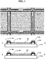
- FIG. 1 shows a plane diagram and a sectional diagram disposing main constitutions of the organic light emitting device according to one embodiment of the present specification. Specifically, FIG. 1 illustrates one example of the constitutions of a substrate, a first electrode, an auxiliary electrode and an insulation layer.
- FIG. 1 Dark regions of FIG. 1 are regions in which a first electrode (201, 501) is not formed, and represent an insulation layer (401).
- an auxiliary electrode (301) is provided on a substrate (101), and the insulation layer (401) covers the auxiliary electrode (301).
- contact holes (601) are formed in some regions of the insulation layer (401), and provide a path capable of connecting the auxiliary electrode (301) and the conductive connection (501).
- an insulation layer is formed on the conductive connection, and an auxiliary electrode may be provided on the insulation layer.
- FIG. 2 illustrates one example of the organic light emitting device further including, in the constitution of the sectional diagram of FIG. 1 , an organic material layer (801) and a second electrode (901) consecutively provided on the conductive unit (201).
- the organic light emitting device may be sealed with an encapsulation layer in the constitution of FIG. 2 .
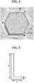
- FIG. 3 and FIG. 4 show any one conductive unit of a first electrode of the organic light emitting device according to one embodiment of the present specification.
- a conductive unit (201) is formed adjoining a conductive connection (501), the conductive connection (501) includes two high resistance regions (511), and the conductive connection (501) may be electrically connected to an auxiliary electrode through contact holes (601).
- the conductive unit may be included in a light emitting region of the organic light emitting device.
- the light emitting region may include each pixel region of the organic light emitting device, and at least one region of each of the conductive units may be located in the light emitting region of the organic light emitting device.
- a light emission phenomenon occurs in an organic material layer including a light emitting layer formed on a region forming the conductive unit, and light may emit through the conductive unit.
- the light emitting region in the present specification means a region in which light emitting at a light emitting layer of an organic material layer emits through a first electrode and/or a second electrode.
- the light emitting region may be formed in at least some of the first electrode region in which an auxiliary electrode is not formed among the regions in which the first electrode is formed on a substrate.
- a non-light emitting region in the present specification may mean the remaining regions excluding the light emitting region.
- the non-light emitting region of the organic light emitting device may mean a region in which an auxiliary electrode is formed.
- Short defects may occur when a second electrode is directly in contact with a first electrode.
- short defects may also occur when an organic material layer loses the function due to a thickness decrease, deformation or the like of the organic material layer located between a first electrode and a second electrode, and the first electrode is in contact with the second electrode.
- a low path is provided to the current of an organic light emitting device, and the organic light emitting device may not normally operate. Due to a leakage current in which a current directly flows from a first electrode to a second electrode due to short defects, the current of an organic light emitting device may flow avoiding a defectless area. This may decrease light emission output of the organic light emitting device, and in many cases, the organic light emitting device may not operate.
- a current used to dispersively flow to a large area of organic materials flows intensively to a short circuit occurring location, high heat is generated locally causing a risk of device breakage or fire.
- the conductive connection includes a high resistance region, thereby is capable of controlling the quantity of a leakage current so that it does not increase infinitely. Accordingly, in the organic light emitting device of the present specification, the remaining conductive units having no short defects may normally operate even when short defects occur in some of the conductive units.
- the conductive connection performs a role of preventing a current escaping through a short defect region by applying moderate resistance when short defects occur by a high resistance region that has a high resistance value.
- the resistance value of the high resistance region may be determined considering leakage current control due to short defects, and a driving voltage increase generated due to the high resistance region when no short defects occur.
- the conductive units may be electrically parallel connected.
- the conductive connection may electrically connect the auxiliary electrode and the conductive unit.
- the conductive connection may physically connect the conductive units to each other.
- a current may flow from the auxiliary electrode to the conductive unit through the conductive connection including a high resistance region. More specifically, when a voltage is applied to the organic light emitting device through external power, a current flow of any one conductive unit may be in a direction of an auxiliary electrode ⁇ a conductive connection ⁇ a conductive unit ⁇ an organic material layer ⁇ a second electrode, or a direction reverse thereto.
- Each of the conductive units of the present specification is separated from each other, and a current may be supplied to each of the conductive units from the auxiliary electrode through the conductive connection. This is for preventing the whole organic light emitting device not operating, when a short circuit occurs in any one conductive unit, by a current having to flow to another unit not experiencing a short circuit flows to the conductive unit experiencing a short circuit.
- the any one or more conductive units may be included in one pixel of the organic light emitting device.
- the conductive unit may perform a role of a transparent electrode of each pixel.
- the conductive connection includes two or more high resistance regions.
- each of the conductive connections has two or more high resistance regions, and therefore, there is an advantage in that, even when any one high resistance region of the conductive connection connected to each conductive unit is disconnected, the conductive unit may normally operate by the remaining high resistance regions.
- each of the conductive units is electrically connected to an auxiliary electrode by a high resistance region having the lowest resistance value among the two or more high resistance regions that are not disconnected.
- the conductive connection may be provided on a non-light emitting region provided with the auxiliary electrode.
- the high resistance region may be provided on a non-light emitting region provided with the auxiliary electrode. Accordingly, in the plane diagram of the organic light emitting device, a decrease in an aperture ratio due to the high resistance region may be minimized by the high resistance region being located on a region in which the auxiliary electrode is formed.
- the conductive connection of the present specification may be an end portion of the conductive unit, and the shape or the location is not particularly limited.
- the conductive connection may have a form projected in the middle of one vertex, one edge or one side of a conductive unit having a polygonal shape including a quadrangle.
- the conductive connection includes a high resistance region in which a length of a current flowing direction is longer than a width of a direction vertical thereto.
- the high resistance region includes a region in which a ratio of the length and the width is 10:1 or greater.
- the conductive connection of the present specification may have relatively higher resistance compared to the conductive unit. Moreover, the conductive connection of the present specification may perform a short circuit preventing function in the organic light emitting device. In other words, when short defects occur in an organic light emitting device, the conductive connection of the present specification performs a role of enabling the operation of the device despite the short defects.
- a material of the conductive connection may be the same as a material of the conductive unit.
- the conductive connection and the conductive unit are included in the first electrode, and may be formed with the same material.
- the length and the width of the present specification is a relative concept, and the length may mean a spatial distance from one end to the other end of the conductive connection when seen from the top. In other words, even when the conductive connection is a combination of straight lines or includes curves, the length may mean a value measuring the length assuming a straight line.
- the width in the present specification may mean a distance from the center of the length direction to both ends of the vertical direction of the conductive connection when seen from the top.
- One example of the length and the width is illustrated in FIG. 5 .
- the length of the present specification may mean a measurement of a current flowing direction.
- the width of the present specification may mean a measurement of a direction vertical to the current flowing direction.
- the length of the present specification may mean a distance that a current migrates from the auxiliary electrode to the conductive unit, and the width may mean a distance vertical to the length direction.
- the distance may be a sum of a and b, and the width may be c.
- the conductive connection may physically adjoin the auxiliary electrode through the contact holes.
- the contact holes (601) area in FIG. 3 and FIG. 4 is filled with a conductive connection (501), and adjoins a lower auxiliary electrode and the conductive connection (501).
- the insulation layer may insulate a surface excluding a surface of the auxiliary electrode or the first electrode adjoining the substrate, or a region in which the auxiliary electrode or the first electrode adjoins the contact holes.
- the insulation layer is provided covering an exposed surface of the conductive connection or the auxiliary electrode provided on a substrate, and may provide contact holes through which the conductive connection and the auxiliary electrode are exposed to the outside by removing at least one region of the insulation layer.
- the contact holes may become a path electrically connecting the conductive connection and the auxiliary electrode.
- the contact holes may be a region capable of physically connecting the auxiliary electrode to the first electrode.
- the contact holes of the present specification may become means for preventing a decrease in the aperture ratio of the organic light emitting device by the conductive connection, and the contact holes may be provided on an upper surface or lower surface of the auxiliary electrode. Specifically, the contact holes may be located in a non-light emitting region in which the auxiliary electrode is formed. Moreover, in order to prevent a decrease in the aperture ratio of the organic light emitting device due to the contact holes, a maximum diameter of the contact holes may not be greater than a line width of the auxiliary electrode.
- an additional insulation layer insulating the conductive connection and the organic material layer may be further provided in the organic light emitting device. Specifically, after forming the auxiliary electrode and the first electrode, an additional insulation layer may be provided on the first electrode and/or the auxiliary electrode excluding a region provided with the conductive unit. This is for insulating the organic material layer provided on the first electrode and/or the auxiliary electrode, and the conductive connection.
- the insulation layer and the additional insulation layer may each be an organic insulation layer or an inorganic insulation layer.
- Materials of the insulation layer and the additional insulation layer are not limited as along as the materials are generally used in the art.
- resistance from the auxiliary electrode to the conductive unit may be greater than or equal to 1 k ⁇ and less than or equal to 1 M ⁇ .
- the any one conductive unit and adjacent another conductive unit may mean any one conductive unit and physically closest another conductive unit.
- the first electrode may include 1,000 or more of the conductive units separated from each other. Specifically, the first electrode may include greater than or equal to 1,000 and less than or equal to 1,000,000 of the conductive units separated from each other.
- the first electrode may be formed with patterns of two or more of the conductive units.
- the conductive unit may be formed with patterns in which regions excluding the conductive connection are separated from each other.
- the pattern of the present specification may have the shape of a closed figure.
- the pattern may be a polygon such as a triangle, a quadrangle and a hexagon, or may be an amorphous form.
- FIG. 6 to FIG. 11 show the shapes of a first electrode in the organic light emitting device according to one embodiment of the present specification.
- FIG. 6 and FIG. 7 show cases of the conductive unit (201) forming a triangular pattern.
- FIG. 8 and FIG. 9 show cases of the conductive unit (201) forming a quadrangular pattern.
- FIG. 10 and FIG. 11 show cases of the conductive unit (201) forming a hexagonal pattern.
- those represented as circles or ellipses mean contact holes (601) being provided, and those represented as arrows show a conductive connection (501), and the direction of the arrows shows a direction of a current flowing to the conductive unit (201) through the conductive connection (501).
- the shape of the first electrode of the organic light emitting device is not limited to those in FIG. 6 to FIG. 11 , and various shapes may be provided.
- the number of the contact holes of the organic light emitting device and the disposition of the conductive connection and the like are not limited to those in FIG. 6 to FIG. 11 , and various shapes may be provided.
- the number of the conductive units of the present specification is 1,000 or greater, an effect of the organic light emitting device minimizing a leakage current quantity during the occurrence of a short circuit while minimizing a voltage increase during normal operation may be obtained.
- the effect may be maintained while maintaining an aperture ratio. In other words, when the number of the conductive units is greater than 1,000,000, a decrease in the aperture ratio may occur due to the increase in the number of auxiliary electrodes.
- the area the conductive units occupy in the organic light emitting device may be greater than or equal to 50% and less than or equal to 90% based on the plane diagram of the whole organic light emitting device.
- the conductive unit is included in a light emitting region, and the area the conductive units occupy may be the same as or similar to an aperture ratio of the organic light emitting device based on the light emitting surface of the whole organic light emitting device.
- each of the conductive units is electrically connected by the conductive connection, and therefore, a driving voltage of a device increases. Therefore, according to one embodiment of the present specification, the first electrode may have a short circuit preventing function by the conductive connection while lowering a driving voltage of the device by including 1,000 or more of the conductive units in order to complement a driving voltage increase by the conductive connection.
- an area of each of the conductive units may be greater than or equal to 0.01 mm 2 and less than or equal to 25 mm 2 .
- the conductive connection, the conductive unit, and an organic material layer including a light emitting layer may be electrically series connected to each other.
- the light emitting layer of the present specification is located between the first electrode and the second clcctrodc, and the two or more light emitting layers may be electrically parallel connected to each other.
- the light emitting layer is located between the conductive unit and the second electrode, and each of the light emitting layers may be electrically parallel connected to each other.
- the light emitting layer of the present specification may be located corresponding to a region corresponding to the conductive unit.
- the light emitting layer of the present specification operates at the same current density, a resistance value increases as the area of the light emitting layer decreases.
- the area of each of the conductive units becomes smaller and the number increases, the area of each of the light emitting layers also becomes smaller.
- the ratio of the voltage of the conductive connection series connected to the organic material layer decreases compared to the voltage applied to the organic material layer including the light emitting layer when the organic light emitting device operates.
- the leakage current quantity may be determined by a resistance value and an operating voltage from the auxiliary electrode to the conductive unit regardless of the number of the conductive units. Accordingly, a voltage increase phenomenon by the conductive connection during normal operation may be minimized when increasing the number of the conductive units, and the leakage current quantity may also be minimized when a short circuit occurs.
- the auxiliary electrode may have sheet resistance of 3 ⁇ / ⁇ or less. Specifically, the auxiliary electrode may have sheet resistance of 1 ⁇ / ⁇ or less.
- an auxiliary electrode may be used.
- the sheet resistance of the auxiliary electrode of the present specification may be 3 ⁇ / ⁇ or less, and specifically 1 ⁇ / ⁇ or less, and in the above-mentioned range, the organic light emitting device may maintain high brightness uniformity.
- the first electrode may be formed as a transparent electrode.
- sheet resistance of the first electrode may be higher than sheet resistance required for the operation of the organic light emitting device. Accordingly, in order to lower the sheet resistance of the first electrode, the sheet resistance of the first electrode may be lowered to the sheet resistance level of the auxiliary electrode by electrically connecting the auxiliary electrode to the first electrode.
- the auxiliary electrode may be formed with conductive lines electrically connected to each other.
- the conductive lines may be formed with conductive patterns.
- the whole auxiliary electrode may be driven by applying a voltage to at least one region of the auxiliary electrode of the present specification.
- the organic light emitting device may be used as being included in OLED illumination.
- OLED illumination light emission with uniform brightness in the whole light emitting region, that is, in all the organic light emitting devices, is important.
- voltages formed between the first electrode and the second electrode of all the organic light emitting devices included in the OLED illumination are preferably maintained to be the same.
- the second electrode of each organic light emitting device when the first electrode is a transparent electrode, and the second electrode is a metal electrode, the second electrode of each organic light emitting device has sufficiently low sheet resistance, and there is almost no voltage difference in the second electrode of each of the organic light emitting devices, however, in the case of the first electrode, a voltage difference may exist in each of the organic light emitting devices.
- the auxiliary electrode and specifically, a metal auxiliary electrode, may be used in order to complement the first electrode voltage difference of each of the organic light emitting devices.
- the metal auxiliary electrode may be formed with conductive lines electrically connected to each other.
- the auxiliary electrode is capable of allowing almost no voltage difference in the first electrode of each organic light emitting device by forming conductive lines.
- the conductive unit may have sheet resistance of 1 ⁇ / ⁇ or greater, or 3 ⁇ / ⁇ or greater, and specifically, may be 10 ⁇ / ⁇ or greater.
- the conductive unit may have sheet resistance of 1,000 ⁇ / ⁇ or less, or 500 ⁇ / ⁇ or less.
- the conductive unit may have sheet resistance of greater than or equal to 1 ⁇ / ⁇ and less than or equal to 1,000 ⁇ / ⁇ , or greater than or equal to 10 ⁇ / ⁇ and less than or equal to 500 ⁇ / ⁇ .
- the sheet resistance level required for the conductive unit may be controlled so as to be inversely proportional to an area of the conductive unit corresponding to a light emitting area.
- the sheet resistance required for the conductive unit may be approximately 1 ⁇ / ⁇ .
- the sheet resistance required for the conductive unit may be 1 ⁇ / ⁇ or greater.
- an auxiliary electrode may be used so that the sheet resistance of the conductive unit satisfies 1 ⁇ / ⁇ or greater.
- the auxiliary electrode may be a metal auxiliary electrode.
- the sheet resistance of the conductive unit of the present specification may be determined by materials forming the conductive unit, and may also be lowered to a sheet resistance level of an auxiliary electrode by being electrically connected to the auxiliary electrode. Accordingly, the sheet resistance value of the conductive unit required in the organic light emitting device of the present specification may be adjusted by the materials of the auxiliary electrode and the conductive unit.
- the auxiliary electrode may be formed as a stripe structure or mesh structure.
- the conductive unit may be provided in empty space of the mesh.
- the auxiliary electrode may have a line width of greater or equal to 1 ⁇ m and less than or equal to 100 ⁇ m.
- the line width of the auxiliary electrode may mean a line thickness of the auxiliary electrode based on the parallel section of a substrate surface provided with the auxiliary electrode.
- the line width of the auxiliary electrode may mean the thickest line thickness of the auxiliary electrode based on the parallel section of a substrate surface provided with the auxiliary electrode.
- auxiliary electrode When the auxiliary electrode is formed to have the line width in the above-mentioned range, efficiency of the organic light emitting device may increase by securing an aperture ratio.
- the auxiliary electrode may be provided as a mesh structure surrounding one or more of the conductive units.
- the auxiliary electrode may be provided as a mesh structure forming repeated pattern units of a triangle, a quadrangle or a hexagon.
- the mesh structure may form an aperture region having a repeated shape of a triangle, a quadrangle, a hexagon or the like.
- the pattern unit may mean a repeated closed region formed by the auxiliary electrode.
- the auxiliary electrode may have an aperture ratio of 60% or greater. Specifically, the auxiliary electrode may have an aperture ratio of 70%, or 80% or greater.
- the organic light emitting device may have an aperture ratio of 60% or greater based on the light emitting surface.
- the high resistance region may have a line width of greater than or equal to 0.5 ⁇ m and less than or equal to 100 ⁇ m.
- the high resistance region may be located on a region provided with the auxiliary electrode in order to secure an aperture ratio. Accordingly, the high resistance region may have the same as or smaller than a line width of the auxiliary electrode.
- the first electrode may be a transparent electrode.
- the first electrode When the first electrode is a transparent electrode, the first electrode may be a conductive oxide such as indium tin oxide (ITO) or indium zinc oxide (IZO). Moreover, the first electrode may be a semi-transparent electrode. When the first electrode is a semi-transparent electrode, the first electrode may be prepared with a semi-transparent metal such as Ag, Au, Mg, Ca or alloys thereof. When a semi-transparent metal is used as the first electrode, the organic light emitting device may have a microcavity structure.
- ITO indium tin oxide
- IZO indium zinc oxide
- the first electrode may be a semi-transparent electrode.
- the first electrode When the first electrode is a semi-transparent electrode, the first electrode may be prepared with a semi-transparent metal such as Ag, Au, Mg, Ca or alloys thereof.
- the organic light emitting device When a semi-transparent metal is used as the first electrode, the organic light emitting device may have a microcavity structure.
- the auxiliary electrode may be formed with metal materials.
- the auxiliary electrode may be a metal electrode.
- the auxiliary electrode may generally use all metals. Specifically, aluminum, copper and/or silver having favorable conductivity may be included. When the auxiliary electrode uses aluminum for adhesion with a transparent electrode or stability in a photo process, a molybdenum/aluminum/molybdenum layer may also be used.
- the organic material layer includes at least one or more light emitting layers, and may further include one, two or more types selected from the group consisting of a hole injection layer; a hole transfer layer; a hole blocking layer; a charge generating layer; an electron blocking layer; an electron transfer layer; and an electron injection layer.
- the charge generating layer means a layer generating holes and electrons when a voltage is applied.
- a substrate having excellent transparency, surface smoothness, handling easiness and water resistance may be used.
- a glass substrate, a thin glass substrate or a transparent plastic substrate may be used.
- the plastic substrate may include a film such as polyethylene terephthalate (PET), polyethylene naphthalate (PEN), polyether ether ketone (PEEK) and polyimide (PI) in the form of a single layer or multilayer.
- the substrate may include a light scattering function in the substrate itself.
- the substrate is not limited thereto, and substrates commonly used in organic light emitting devices may be used.
- the first electrode may be an anode, and the second electrode may be a cathode.
- the first electrode may be a cathode, and the second electrode may be an anode.
- anode a material having large work function is normally preferable so that hole injection to the organic material layer is smooth.
- the anode material capable of being used in the present invention include metals such as vanadium, chromium, copper, zinc and gold, or alloys thereof; metal oxides such as zinc oxides, indium oxides, indium tin oxides (ITO) and indium zinc oxide (IZO); combinations of metals and oxides such as ZnO:Al or SnO 2 :Sb; conductive polymers such as poly(3-methylthiophene), poly[3,4-(ethylen-1,2-dioxy)thiophene] (PEDOT), polypyrrole and polyaniline, and the like, but are not limited thereto.
- the materials of the anode are not limited to the anode, and may be used as a material of the cathode.
- the cathode a material having small work function is normally preferable so that electron injection to the organic material layer is smooth.
- the cathode material include metals such as magnesium, calcium, sodium, potassium, titanium, indium, yttrium, lithium, gadolinium, aluminum, silver, tin and lead, or alloys thereof; multilayer structure materials such as LiF/Al or LiO 2 /Al, and the like, but are not limited thereto.
- the materials of the cathode are not limited to the cathode, and may be used as a material of the anode.
- the hole transfer layer material As the hole transfer layer material according to the present specification, a material capable of receiving the holes from the anode or the hole injection layer, moving the holes to the light emitting layer, and having high mobility for the holes, is suitable. Specific examples thereof include an arylamin-based organic material, a conductive polymer, a block copolymer having conjugated parts and non-conjugated parts together, and the like, but are not limited thereto.
- a material capable of emitting light in a visible region by receiving holes and electrons from the hole transfer layer and the electron transfer layer, respectively, and binding the holes and the electrons and is preferably a material having favorable quantum efficiency for fluorescence or phosphorescence.
- Specific examples thereof include a 8-hydroxy-quinoline aluminum complex (Alq 3 ); a carbazolc-bascd compound; a dimcrizcd styryl compound; BAlq; a 10-hydroxybenzo quinolin-metal compound; a benzoxazole-, a benzthiazole- and a benzimidazole-based compound; a poly(p-phenylenevinylene) (PPV)-based polymer; a spiro compound; polyfluorene, rubrene, and the like, but are not limited thereto.
- Alq 3 8-hydroxy-quinoline aluminum complex
- a carbazolc-bascd compound a dimcrizcd styryl compound
- BAlq a 10-hydroxybenzo quinolin-metal compound
- a benzoxazole-, a benzthiazole- and a benzimidazole-based compound a poly(p-phenylenevinylene) (PPV)-based poly
- the electron transfer layer material As the electron transfer layer material according to the present specification, a material capable of favorably receiving electrons from the cathode, moving the electrons to the light emitting layer, and having high mobility for the electrons, is suitable. Specific examples thereof include an Al complex of 8-hydroxyquinoline; a complex including Alq 3 ; an organic radical compound; a hydroxyflavon-metal complex and the like, but are not limited thereto.
- the auxiliary electrode may be located in a non-light emitting region of the organic light emitting device.
- the organic light emitting device may be sealed with an encapsulation layer.
- the encapsulation layer may be formed with a transparent resin layer.
- the encapsulation layer performs a role of preventing the organic light emitting device from oxygen and contaminants, and may be a transparent material so as not to inhibit light emission of the organic light emitting device.
- the transparency may mean transmitting 60% or more of light, and specifically, transmitting 75% or more of light.
- the organic light emitting device may emit white light having a color temperature of greater than or equal to 2,000 K and less than or equal to 12,000 K.
- a light scattering layer may be further included between the substrate and the first electrode.
- a substrate provided on a surface opposite to the surface provided with the organic material layer of the first electrode may be further included, and a light scattering layer provided between the substrate and the first electrode may be further included.
- the light scattering layer may include a planarization layer.
- the planarization layer may be provided between the first electrode and the light scattering layer.
- a light scattering layer may be further included on a surface opposite to the surface provided with the first electrode of the substrate.
- the light scattering layer induces light scattering
- the structure is not particularly limited as long as it has a structure capable of enhancing light scattering efficiency of the organic light emitting dcvicc.
- the light scattering layer may have a structure in which scattered particles are dispersed into a binder, a film having unevenness, and/or a film having hazeness.
- the light scattering layer may be directly formed on the substrate using a method such as spin coating, bar coating and slit coating, or may be formed using a method of being prepared in a film form and attached.
- the organic light emitting device may be a flexible organic light emitting device.
- the substrate may include a flexible material.
- the substrate may be bendable thin-film-type glass, a plastic substrate or film-type substrate.
- a material of the plastic substrate is not particularly limited, however, a film such as polyethylene terephthalate (PET), polyethylene naphthalate (PEN), polyether ether ketone (PEEK) and polyimide (PI) may be generally included in the form of a single layer or multilayer.
- PET polyethylene terephthalate
- PEN polyethylene naphthalate
- PEEK polyether ether ketone
- PI polyimide
- the present specification provides a display device including the organic light emitting device.
- the organic light emitting device may perform a role of a pixel or back light in the display device.
- constitutions known in the art may be used.
- the present specification provides an illumination device including the organic light emitting device.
- the organic light emitting device may perform a role of a light emitting unit in the illumination device.
- constitutions known in the art may be used.
- One embodiment of the present specification provides a method for manufacturing the organic light emitting device including preparing a substrate; forming an auxiliary electrode on the substrate; forming a first electrode including two or more conductive units provided to be separated from each other and a conductive connection connected to the conductive units on the substrate; forming an insulation layer including one or more contact holes on the conductive connection or the auxiliary electrode; forming one or more organic material layers on the first electrode; and forming a second electrode on the organic material layers, wherein the conductive connection is electrically connected to the auxiliary electrode through the contact holes, and the conductive connection includes one or more high resistance regions in which a length of a current flowing direction is longer than a width of a direction vertical thereto.
- the forming of an auxiliary electrode may use photo etching; deposition; or printing.
- the forming of an auxiliary electrode may use a method for forming the auxiliary electrode as a stripe structure or mesh structure.
- the photo etching, deposition and printing methods generally used in the art may be used without limits.
- the forming of an insulation layer may be forming an insulation layer so as to cover the conductive connection or the auxiliary electrode, and then forming the contact holes by removing one region of the insulation layer.
- the forming of a first electrode may be forming a first electrode material layer on the substrate, and patterning the layer into the first electrode. Specifically, a first electrode material layer is formed on the substrate, and the first electrode material layer may be formed into the first electrode through photo etching, laser etching or the like. Moreover, after forming the first electrode on the substrate, an insulation layer may be formed the conductive connection, and an auxiliary electrode may be formed on the insulation layer.
- the forming of a first electrode may be forming, after the forming of an insulation layer, a first electrode material layer on the substrate on which the auxiliary electrode and the insulation layer are formed, and patterning the layer into the first electrode.
- the forming of a first electrode may be forming, after the forming of an insulation layer, a first electrode material layer using a deposition process, and forming the first electrode material layer into the first electrode through photo etching, laser etching or the like.
Landscapes
- Physics & Mathematics (AREA)
- Optics & Photonics (AREA)
- Engineering & Computer Science (AREA)
- Microelectronics & Electronic Packaging (AREA)
- Electroluminescent Light Sources (AREA)
Claims (15)
- Dispositif électroluminescent organique comportant :un substrat (101) ;une première électrode (201, 501) agencée sur le substrat (101), et incluant deux unités conductrices (201) ou plus agencées de manière à être séparées les unes des autres et une connexion conductrice (501) connectée aux unités conductrices (201) ;une électrode auxiliaire (301) agencée sur le substrat (101), et disposée de manière à être séparée des unités conductrices (201) ;une couche d'isolation (401) agencée sur la connexion conductrice (501) ou l'électrode auxiliaire (301), et incluant un ou plusieurs trous de contact (601) exposant une zone de la connexion conductrice (501) ou de l'électrode auxiliaire (301) ;une seconde électrode (901) agencée opposée à la première électrode (201, 205) ; etune ou plusieurs couches de matériau organique (801) agencées entre la première électrode (201, 501) et la seconde électrode (901),dans lequel la connexion conductrice (501) est électriquement connectée à l'électrode auxiliaire (301) à travers les trous de contact (601) ;caractérisé en ce quela connexion conductrice (501) inclut deux zones à résistance élevée (511) ou plus dans lesquelles une longueur d'une direction de circulation de courant est plus longue qu'une largeur d'une direction verticale à celle-ci, de telle sorte que lorsqu'une zone à résistance élevée quelconque de la connexion conductrice (501) connectée à une unité conductrice (201) est déconnectée, l'unité conductrice (201) fonctionne normalement par l'intermédiaire des zones à résistance élevée (511) restantes,dans lequel chacune des unités conductrices (201) est électriquement connectée à l'électrode auxiliaire (301) par une zone à résistance élevée ayant la plus faible valeur de résistance parmi les deux zones à résistance élevée ou plus,dans lequel les deux zones à résistance élevée (511) ou plus de la connexion conductrice (501) suivent un contour de l'électrode auxiliaire (301), etdans lequel la zone à résistance élevée inclut une zone dans laquelle un rapport de la longueur et de la largeur est de 10:1 ou plus.
- Dispositif électroluminescent organique selon la revendication 1, dans lequel au moins une partie de la connexion conductrice est agencée sur une zone non électroluminescente pourvue de l'électrode auxiliaire.
- Dispositif électroluminescent organique selon la revendication 1, dans lequel la connexion conductrice (501) connecte électriquement l'électrode auxiliaire (301) et l'unité conductrice (201).
- Dispositif électroluminescent organique selon la revendication 1, dans lequel la connexion conductrice (501) jouxte physiquement l'électrode auxiliaire (301) à travers les trous de contact (601).
- Dispositif électroluminescent organique selon la revendication 1, dans lequel la couche d'isolation (401) isole une surface excluant une surface de l'électrode auxiliaire (301) ou de la première électrode (201, 501) jouxtant le substrat (101), ou une zone dans laquelle l'électrode auxiliaire (301) ou la première électrode (201, 501) jouxte les trous de contact (601).
- Dispositif électroluminescent organique selon la revendication 1, comportant en outre une couche d'isolation supplémentaire (701) isolant la connexion conductrice (501) et la couche de matériau organique (801).
- Dispositif électroluminescent organique selon la revendication 1, dans lequel l'électrode auxiliaire est fournie sous la forme d'une structure en treillis entourant une ou plusieurs des unités conductrices.
- Dispositif électroluminescent organique selon la revendication 1, dans lequel l'électrode auxiliaire (301) est fournie sous la forme d'une structure en treillis formant des unités à motif répété d'un triangle, d'un quadrangle ou d'un hexagone.
- Dispositif électroluminescent organique selon la revendication 1, qui est un dispositif électroluminescent organique souple.
- Dispositif d'affichage comportant le dispositif électroluminescent organique selon l'une quelconque des revendications 1 à 9.
- Dispositif d'éclairage comportant le dispositif électroluminescent organique selon l'une quelconque des revendications 1 à 9.
- Procédé pour fabriquer le dispositif électroluminescent organique selon l'une quelconque des revendications 1 à 9 comportant les étapes consistant à :préparer un substrat (101) ;former une électrode auxiliaire (301) sur le substrat (101) ;former une couche d'isolation (401) incluant un ou plusieurs trous de contact (601) sur l'électrode auxiliaire (301) ;former une première électrode (201, 501) incluant deux unités conductrices (201) ou plus agencées de manière à être séparées les unes des autres et une connexion conductrice (501) connectée aux unités conductrices (201) ;former une ou plusieurs couches de matériau organique (801) sur la première électrode (201, 501) ; etformer une seconde électrode (901) sur les couches de matériau organique (801),dans lequel la connexion conductrice (501) est électriquement connectée à l'électrode auxiliaire (301) à travers les trous de contact (601) ;caractérisé en ce quela connexion conductrice (501) inclut deux zones à résistance élevée (511) ou plus dans lesquelles une longueur d'une direction de circulation de courant est plus longue qu'une largeur d'une direction verticale à celle-ci, de telle sorte que lorsqu'une zone à résistance élevée quelconque de la connexion conductrice (501) connectée à une unité conductrice (201) est déconnectée, l'unité conductrice (201) est configurée pour fonctionner normalement par l'intermédiaire des zones à résistance élevée (511) restantes,dans lequel les unités conductrices (201) sont électriquement connectées à une électrode auxiliaire (301) par une zone à résistance élevée ayant la plus faible valeur de résistance parmi les deux zones à résistance élevée ou plus,dans lequel les deux zones à résistance élevée (511) ou plus de la connexion conductrice (501) suivent un contour de l'électrode auxiliaire (301), etdans lequel la zone à résistance élevée inclut une zone dans laquelle un rapport de la longueur et de la largeur est de 10:1 ou plus.
- Procédé pour fabriquer le dispositif électroluminescent organique selon la revendication 12, dans lequel la formation d'une couche d'isolation (401) consiste à former une couche d'isolation de manière à recouvrir l'électrode auxiliaire (301), et à ensuite former les trous de contact (601) en retirant une zone de la couche d'isolation (401).
- Procédé pour fabriquer le dispositif électroluminescent organique selon la revendication 12, dans lequel la formation d'une première électrode (201, 501) consiste à former une première couche de matériau d'électrode sur le substrat (101), et former un motif sur la couche dans la première électrode (201, 501).
- Procédé pour fabriquer le dispositif électroluminescent organique selon la revendication 12, dans lequel la formation d'une première électrode (201, 501) consiste à former, après la formation d'une couche d'isolation (401), une première couche de matériau d'électrode sur le substrat (101) sur lequel l'électrode auxiliaire (301) et la couche d'isolation (401) sont formées, et former un motif sur la couche dans la première électrode (201, 501).
Applications Claiming Priority (2)
| Application Number | Priority Date | Filing Date | Title |
|---|---|---|---|
| KR1020140056776A KR102101644B1 (ko) | 2014-05-12 | 2014-05-12 | 유기발광소자 및 이의 제조방법 |
| PCT/KR2015/004480 WO2015174672A1 (fr) | 2014-05-12 | 2015-05-04 | Dispositif organique électroluminescent et son procédé de fabrication |
Publications (3)
| Publication Number | Publication Date |
|---|---|
| EP3144995A1 EP3144995A1 (fr) | 2017-03-22 |
| EP3144995A4 EP3144995A4 (fr) | 2017-11-01 |
| EP3144995B1 true EP3144995B1 (fr) | 2021-09-08 |
Family
ID=54480168
Family Applications (1)
| Application Number | Title | Priority Date | Filing Date |
|---|---|---|---|
| EP15793385.4A Active EP3144995B1 (fr) | 2014-05-12 | 2015-05-04 | Dispositif organique électroluminescent et son procédé de fabrication |
Country Status (7)
| Country | Link |
|---|---|
| US (1) | US10325975B2 (fr) |
| EP (1) | EP3144995B1 (fr) |
| JP (1) | JP6559708B2 (fr) |
| KR (1) | KR102101644B1 (fr) |
| CN (1) | CN106463645B (fr) |
| TW (1) | TWI590508B (fr) |
| WO (1) | WO2015174672A1 (fr) |
Families Citing this family (11)
| Publication number | Priority date | Publication date | Assignee | Title |
|---|---|---|---|---|
| CN109148509B (zh) * | 2017-06-27 | 2020-09-22 | 固安翌光科技有限公司 | 一种有机电致发光器件 |
| KR102413156B1 (ko) * | 2017-11-28 | 2022-06-24 | 엘지디스플레이 주식회사 | Oled 조명 장치 |
| CN109065750B (zh) * | 2018-07-25 | 2020-04-21 | 固安翌光科技有限公司 | 一种有机电致发光器件及其加工方法 |
| CN109449179A (zh) * | 2018-10-22 | 2019-03-08 | 固安翌光科技有限公司 | 一种无源有机电致发光器件 |
| TWI677123B (zh) * | 2018-11-29 | 2019-11-11 | 機光科技股份有限公司 | 去定位器及使用該去定位器的發光裝置 |
| CN111244299A (zh) * | 2018-11-29 | 2020-06-05 | 机光科技股份有限公司 | 去定位器及使用该去定位器的发光装置 |
| KR102740796B1 (ko) * | 2018-12-24 | 2024-12-09 | 엘지디스플레이 주식회사 | 전계 발광 조명장치 |
| KR102544067B1 (ko) * | 2018-12-31 | 2023-06-16 | 엘지디스플레이 주식회사 | 유기 조명 장치 |
| KR102427008B1 (ko) | 2019-12-02 | 2022-08-01 | 도레이 카부시키가이샤 | 감광성 조성물, 네거티브형 감광성 조성물, 화소 분할층 및 유기 el 표시 장치 |
| CN113346032B (zh) * | 2021-06-01 | 2023-04-07 | 固安翌光科技有限公司 | 一种有机电致发光器件 |
| CN216389372U (zh) * | 2021-09-30 | 2022-04-26 | 武汉华美晨曦光电有限责任公司 | 抗穿击oled电致发光器件 |
Family Cites Families (30)
| Publication number | Priority date | Publication date | Assignee | Title |
|---|---|---|---|---|
| TW364275B (en) * | 1996-03-12 | 1999-07-11 | Idemitsu Kosan Co | Organic electroluminescent element and organic electroluminescent display device |
| JPH10294491A (ja) * | 1997-04-22 | 1998-11-04 | Toshiba Corp | 半導体発光素子およびその製造方法ならびに発光装置 |
| US6713955B1 (en) * | 1998-11-20 | 2004-03-30 | Agilent Technologies, Inc. | Organic light emitting device having a current self-limiting structure |
| JP4608105B2 (ja) * | 1999-04-02 | 2011-01-05 | 出光興産株式会社 | 有機エレクトロルミネッセンス表示装置およびその製造方法 |
| JP3878365B2 (ja) * | 1999-09-09 | 2007-02-07 | 株式会社日立製作所 | 画像表示装置および画像表示装置の製造方法 |
| JP2001196191A (ja) * | 2000-01-14 | 2001-07-19 | Fuji Electric Co Ltd | 有機薄膜発光ディスプレイおよびその製造方法 |
| US20030000669A1 (en) * | 2001-05-11 | 2003-01-02 | Invensys Systems, Inc. | Methods and systems for controlling paper quality by adjusting fiber filter parameters |
| US6664730B2 (en) * | 2001-07-09 | 2003-12-16 | Universal Display Corporation | Electrode structure of el device |
| JP4270891B2 (ja) | 2003-01-21 | 2009-06-03 | 三洋電機株式会社 | El表示装置のレーザーリペア方法 |
| TWI223569B (en) | 2002-03-20 | 2004-11-01 | Sanyo Electric Co | Method for reducing light quantity of organic EL panel and organic EL panel |
| KR100711161B1 (ko) * | 2002-09-12 | 2007-04-24 | 도시바 마쯔시따 디스플레이 테크놀로지 컴퍼니, 리미티드 | 유기 el 디스플레이 |
| US7183707B2 (en) | 2004-04-12 | 2007-02-27 | Eastman Kodak Company | OLED device with short reduction |
| US7586171B2 (en) * | 2004-04-14 | 2009-09-08 | Yong Cao | Organic electronic device comprising conductive members and processes for forming and using the organic electronic device |
| JP4706287B2 (ja) * | 2005-03-11 | 2011-06-22 | セイコーエプソン株式会社 | 有機el装置および電子機器 |
| DE102008013031B4 (de) * | 2008-03-07 | 2019-07-25 | Osram Oled Gmbh | Optoelektronisches Bauelement |
| JP5882738B2 (ja) | 2008-11-25 | 2016-03-09 | コーニンクレッカ フィリップス エヌ ヴェKoninklijke Philips N.V. | 有機発光ダイオードの短絡防止 |
| DE102009001573B3 (de) * | 2009-03-16 | 2010-08-05 | Tyco Electronics Amp Gmbh | Elektrisch leitendes Federelement, Kontaktelement und Steckverbinder |
| KR101254748B1 (ko) | 2009-05-06 | 2013-04-15 | 엘지디스플레이 주식회사 | 유기전계발광표시장치 및 이의 제조방법 |
| US20110193066A1 (en) | 2009-08-13 | 2011-08-11 | E. I. Du Pont De Nemours And Company | Current limiting element for pixels in electronic devices |
| KR101113451B1 (ko) | 2009-12-01 | 2012-02-29 | 삼성모바일디스플레이주식회사 | 유기 전계발광 표시장치 |
| TWI425858B (zh) * | 2010-08-13 | 2014-02-01 | Au Optronics Corp | 有機發光裝置、照明裝置以及液晶顯示器 |
| JP5707928B2 (ja) | 2010-12-21 | 2015-04-30 | セイコーエプソン株式会社 | 照明装置、その製造方法、及び電子機器 |
| US8552440B2 (en) | 2010-12-24 | 2013-10-08 | Semiconductor Energy Laboratory Co., Ltd. | Lighting device |
| JP6057143B2 (ja) | 2012-03-19 | 2017-01-11 | 株式会社Joled | 有機エレクトロルミネッセンス素子 |
| KR101582719B1 (ko) * | 2012-05-31 | 2016-01-05 | 주식회사 엘지화학 | 유기 발광 소자 및 이의 제조방법 |
| JP2014053120A (ja) | 2012-09-06 | 2014-03-20 | Seiko Epson Corp | 有機el装置の製造方法、有機el装置、電子機器 |
| KR101965256B1 (ko) | 2012-10-17 | 2019-04-04 | 삼성디스플레이 주식회사 | 유기 발광 표시 장치 |
| WO2014140672A1 (fr) * | 2013-03-15 | 2014-09-18 | L'air Liquide, Societe Anonyme Pour I'etude Et I'exploitation Des Procedes Georges Claude | Molécules de bis(alkylimido)-bis-(alkylamido) molybdène pour le dépôt de films contenant du molybdène |
| CN105164829B (zh) * | 2013-04-29 | 2016-10-05 | 乐金显示有限公司 | 有机发光器件及其制造方法 |
| CN105210206B (zh) * | 2013-05-16 | 2017-04-05 | 乐金显示有限公司 | 有机发光器件及其制造方法 |
-
2014
- 2014-05-12 KR KR1020140056776A patent/KR102101644B1/ko active Active
-
2015
- 2015-05-04 US US15/310,699 patent/US10325975B2/en active Active
- 2015-05-04 CN CN201580026358.4A patent/CN106463645B/zh active Active
- 2015-05-04 WO PCT/KR2015/004480 patent/WO2015174672A1/fr not_active Ceased
- 2015-05-04 JP JP2016567623A patent/JP6559708B2/ja active Active
- 2015-05-04 EP EP15793385.4A patent/EP3144995B1/fr active Active
- 2015-05-08 TW TW104114645A patent/TWI590508B/zh active
Also Published As
| Publication number | Publication date |
|---|---|
| TWI590508B (zh) | 2017-07-01 |
| TW201607096A (zh) | 2016-02-16 |
| EP3144995A4 (fr) | 2017-11-01 |
| US10325975B2 (en) | 2019-06-18 |
| EP3144995A1 (fr) | 2017-03-22 |
| CN106463645B (zh) | 2020-09-18 |
| US20170077210A1 (en) | 2017-03-16 |
| KR102101644B1 (ko) | 2020-04-17 |
| CN106463645A (zh) | 2017-02-22 |
| JP2017516271A (ja) | 2017-06-15 |
| WO2015174672A1 (fr) | 2015-11-19 |
| JP6559708B2 (ja) | 2019-08-14 |
| KR20150129564A (ko) | 2015-11-20 |
Similar Documents
| Publication | Publication Date | Title |
|---|---|---|
| EP3144995B1 (fr) | Dispositif organique électroluminescent et son procédé de fabrication | |
| EP3144994B1 (fr) | Dispositif organique électroluminescent et son procédé de fabrication | |
| EP3144993B1 (fr) | Élément électroluminescent organique | |
| KR101477929B1 (ko) | 유기발광소자 및 이의 제조방법 | |
| KR101477955B1 (ko) | 유기발광소자 및 이의 제조방법 | |
| KR101469413B1 (ko) | 유기발광소자 및 이의 제조방법 | |
| KR101477953B1 (ko) | 유기발광소자 및 이의 제조방법 | |
| EP3144992B1 (fr) | Dispositif électroluminescent organique | |
| KR20150123599A (ko) | 유기발광소자 | |
| TWI590353B (zh) | 偵測有機發光裝置之短路缺陷區域的方法 |
Legal Events
| Date | Code | Title | Description |
|---|---|---|---|
| STAA | Information on the status of an ep patent application or granted ep patent |
Free format text: STATUS: THE INTERNATIONAL PUBLICATION HAS BEEN MADE |
|
| PUAI | Public reference made under article 153(3) epc to a published international application that has entered the european phase |
Free format text: ORIGINAL CODE: 0009012 |
|
| STAA | Information on the status of an ep patent application or granted ep patent |
Free format text: STATUS: REQUEST FOR EXAMINATION WAS MADE |
|
| 17P | Request for examination filed |
Effective date: 20161110 |
|
| AK | Designated contracting states |
Kind code of ref document: A1 Designated state(s): AL AT BE BG CH CY CZ DE DK EE ES FI FR GB GR HR HU IE IS IT LI LT LU LV MC MK MT NL NO PL PT RO RS SE SI SK SM TR |
|
| AX | Request for extension of the european patent |
Extension state: BA ME |
|
| DAV | Request for validation of the european patent (deleted) | ||
| DAX | Request for extension of the european patent (deleted) | ||
| A4 | Supplementary search report drawn up and despatched |
Effective date: 20170929 |
|
| RIC1 | Information provided on ipc code assigned before grant |
Ipc: H01L 51/52 20060101AFI20170925BHEP Ipc: H01L 51/56 20060101ALI20170925BHEP |
|
| STAA | Information on the status of an ep patent application or granted ep patent |
Free format text: STATUS: EXAMINATION IS IN PROGRESS |
|
| 17Q | First examination report despatched |
Effective date: 20200102 |
|
| GRAJ | Information related to disapproval of communication of intention to grant by the applicant or resumption of examination proceedings by the epo deleted |
Free format text: ORIGINAL CODE: EPIDOSDIGR1 |
|
| STAA | Information on the status of an ep patent application or granted ep patent |
Free format text: STATUS: GRANT OF PATENT IS INTENDED |
|
| GRAP | Despatch of communication of intention to grant a patent |
Free format text: ORIGINAL CODE: EPIDOSNIGR1 |
|
| INTG | Intention to grant announced |
Effective date: 20210517 |
|
| GRAS | Grant fee paid |
Free format text: ORIGINAL CODE: EPIDOSNIGR3 |
|
| GRAA | (expected) grant |
Free format text: ORIGINAL CODE: 0009210 |
|
| STAA | Information on the status of an ep patent application or granted ep patent |
Free format text: STATUS: THE PATENT HAS BEEN GRANTED |
|
| AK | Designated contracting states |
Kind code of ref document: B1 Designated state(s): AL AT BE BG CH CY CZ DE DK EE ES FI FR GB GR HR HU IE IS IT LI LT LU LV MC MK MT NL NO PL PT RO RS SE SI SK SM TR |
|
| REG | Reference to a national code |
Ref country code: GB Ref legal event code: FG4D |
|
| REG | Reference to a national code |
Ref country code: AT Ref legal event code: REF Ref document number: 1429369 Country of ref document: AT Kind code of ref document: T Effective date: 20210915 Ref country code: CH Ref legal event code: EP |
|
| REG | Reference to a national code |
Ref country code: IE Ref legal event code: FG4D |
|
| REG | Reference to a national code |
Ref country code: DE Ref legal event code: R096 Ref document number: 602015073130 Country of ref document: DE |
|
| REG | Reference to a national code |
Ref country code: LT Ref legal event code: MG9D |
|
| REG | Reference to a national code |
Ref country code: NL Ref legal event code: MP Effective date: 20210908 |
|
| PG25 | Lapsed in a contracting state [announced via postgrant information from national office to epo] |
Ref country code: HR Free format text: LAPSE BECAUSE OF FAILURE TO SUBMIT A TRANSLATION OF THE DESCRIPTION OR TO PAY THE FEE WITHIN THE PRESCRIBED TIME-LIMIT Effective date: 20210908 Ref country code: RS Free format text: LAPSE BECAUSE OF FAILURE TO SUBMIT A TRANSLATION OF THE DESCRIPTION OR TO PAY THE FEE WITHIN THE PRESCRIBED TIME-LIMIT Effective date: 20210908 Ref country code: SE Free format text: LAPSE BECAUSE OF FAILURE TO SUBMIT A TRANSLATION OF THE DESCRIPTION OR TO PAY THE FEE WITHIN THE PRESCRIBED TIME-LIMIT Effective date: 20210908 Ref country code: NO Free format text: LAPSE BECAUSE OF FAILURE TO SUBMIT A TRANSLATION OF THE DESCRIPTION OR TO PAY THE FEE WITHIN THE PRESCRIBED TIME-LIMIT Effective date: 20211208 Ref country code: FI Free format text: LAPSE BECAUSE OF FAILURE TO SUBMIT A TRANSLATION OF THE DESCRIPTION OR TO PAY THE FEE WITHIN THE PRESCRIBED TIME-LIMIT Effective date: 20210908 Ref country code: ES Free format text: LAPSE BECAUSE OF FAILURE TO SUBMIT A TRANSLATION OF THE DESCRIPTION OR TO PAY THE FEE WITHIN THE PRESCRIBED TIME-LIMIT Effective date: 20210908 Ref country code: LT Free format text: LAPSE BECAUSE OF FAILURE TO SUBMIT A TRANSLATION OF THE DESCRIPTION OR TO PAY THE FEE WITHIN THE PRESCRIBED TIME-LIMIT Effective date: 20210908 Ref country code: BG Free format text: LAPSE BECAUSE OF FAILURE TO SUBMIT A TRANSLATION OF THE DESCRIPTION OR TO PAY THE FEE WITHIN THE PRESCRIBED TIME-LIMIT Effective date: 20211208 |
|
| REG | Reference to a national code |
Ref country code: AT Ref legal event code: MK05 Ref document number: 1429369 Country of ref document: AT Kind code of ref document: T Effective date: 20210908 |
|
| PG25 | Lapsed in a contracting state [announced via postgrant information from national office to epo] |
Ref country code: LV Free format text: LAPSE BECAUSE OF FAILURE TO SUBMIT A TRANSLATION OF THE DESCRIPTION OR TO PAY THE FEE WITHIN THE PRESCRIBED TIME-LIMIT Effective date: 20210908 Ref country code: GR Free format text: LAPSE BECAUSE OF FAILURE TO SUBMIT A TRANSLATION OF THE DESCRIPTION OR TO PAY THE FEE WITHIN THE PRESCRIBED TIME-LIMIT Effective date: 20211209 |
|
| PG25 | Lapsed in a contracting state [announced via postgrant information from national office to epo] |
Ref country code: AT Free format text: LAPSE BECAUSE OF FAILURE TO SUBMIT A TRANSLATION OF THE DESCRIPTION OR TO PAY THE FEE WITHIN THE PRESCRIBED TIME-LIMIT Effective date: 20210908 |
|
| PG25 | Lapsed in a contracting state [announced via postgrant information from national office to epo] |
Ref country code: IS Free format text: LAPSE BECAUSE OF FAILURE TO SUBMIT A TRANSLATION OF THE DESCRIPTION OR TO PAY THE FEE WITHIN THE PRESCRIBED TIME-LIMIT Effective date: 20220108 Ref country code: SM Free format text: LAPSE BECAUSE OF FAILURE TO SUBMIT A TRANSLATION OF THE DESCRIPTION OR TO PAY THE FEE WITHIN THE PRESCRIBED TIME-LIMIT Effective date: 20210908 Ref country code: SK Free format text: LAPSE BECAUSE OF FAILURE TO SUBMIT A TRANSLATION OF THE DESCRIPTION OR TO PAY THE FEE WITHIN THE PRESCRIBED TIME-LIMIT Effective date: 20210908 Ref country code: RO Free format text: LAPSE BECAUSE OF FAILURE TO SUBMIT A TRANSLATION OF THE DESCRIPTION OR TO PAY THE FEE WITHIN THE PRESCRIBED TIME-LIMIT Effective date: 20210908 Ref country code: PT Free format text: LAPSE BECAUSE OF FAILURE TO SUBMIT A TRANSLATION OF THE DESCRIPTION OR TO PAY THE FEE WITHIN THE PRESCRIBED TIME-LIMIT Effective date: 20220110 Ref country code: PL Free format text: LAPSE BECAUSE OF FAILURE TO SUBMIT A TRANSLATION OF THE DESCRIPTION OR TO PAY THE FEE WITHIN THE PRESCRIBED TIME-LIMIT Effective date: 20210908 Ref country code: NL Free format text: LAPSE BECAUSE OF FAILURE TO SUBMIT A TRANSLATION OF THE DESCRIPTION OR TO PAY THE FEE WITHIN THE PRESCRIBED TIME-LIMIT Effective date: 20210908 Ref country code: EE Free format text: LAPSE BECAUSE OF FAILURE TO SUBMIT A TRANSLATION OF THE DESCRIPTION OR TO PAY THE FEE WITHIN THE PRESCRIBED TIME-LIMIT Effective date: 20210908 Ref country code: CZ Free format text: LAPSE BECAUSE OF FAILURE TO SUBMIT A TRANSLATION OF THE DESCRIPTION OR TO PAY THE FEE WITHIN THE PRESCRIBED TIME-LIMIT Effective date: 20210908 Ref country code: AL Free format text: LAPSE BECAUSE OF FAILURE TO SUBMIT A TRANSLATION OF THE DESCRIPTION OR TO PAY THE FEE WITHIN THE PRESCRIBED TIME-LIMIT Effective date: 20210908 |
|
| REG | Reference to a national code |
Ref country code: DE Ref legal event code: R097 Ref document number: 602015073130 Country of ref document: DE |
|
| PLBE | No opposition filed within time limit |
Free format text: ORIGINAL CODE: 0009261 |
|
| STAA | Information on the status of an ep patent application or granted ep patent |
Free format text: STATUS: NO OPPOSITION FILED WITHIN TIME LIMIT |
|
| PG25 | Lapsed in a contracting state [announced via postgrant information from national office to epo] |
Ref country code: DK Free format text: LAPSE BECAUSE OF FAILURE TO SUBMIT A TRANSLATION OF THE DESCRIPTION OR TO PAY THE FEE WITHIN THE PRESCRIBED TIME-LIMIT Effective date: 20210908 |
|
| 26N | No opposition filed |
Effective date: 20220609 |
|
| PG25 | Lapsed in a contracting state [announced via postgrant information from national office to epo] |
Ref country code: SI Free format text: LAPSE BECAUSE OF FAILURE TO SUBMIT A TRANSLATION OF THE DESCRIPTION OR TO PAY THE FEE WITHIN THE PRESCRIBED TIME-LIMIT Effective date: 20210908 |
|
| REG | Reference to a national code |
Ref country code: DE Ref legal event code: R079 Ref document number: 602015073130 Country of ref document: DE Free format text: PREVIOUS MAIN CLASS: H01L0051520000 Ipc: H10K0050800000 |
|
| REG | Reference to a national code |
Ref country code: CH Ref legal event code: PL |
|
| REG | Reference to a national code |
Ref country code: BE Ref legal event code: MM Effective date: 20220531 |
|
| PG25 | Lapsed in a contracting state [announced via postgrant information from national office to epo] |
Ref country code: MC Free format text: LAPSE BECAUSE OF FAILURE TO SUBMIT A TRANSLATION OF THE DESCRIPTION OR TO PAY THE FEE WITHIN THE PRESCRIBED TIME-LIMIT Effective date: 20210908 Ref country code: LU Free format text: LAPSE BECAUSE OF NON-PAYMENT OF DUE FEES Effective date: 20220504 Ref country code: LI Free format text: LAPSE BECAUSE OF NON-PAYMENT OF DUE FEES Effective date: 20220531 Ref country code: IT Free format text: LAPSE BECAUSE OF FAILURE TO SUBMIT A TRANSLATION OF THE DESCRIPTION OR TO PAY THE FEE WITHIN THE PRESCRIBED TIME-LIMIT Effective date: 20210908 Ref country code: CH Free format text: LAPSE BECAUSE OF NON-PAYMENT OF DUE FEES Effective date: 20220531 |
|
| PG25 | Lapsed in a contracting state [announced via postgrant information from national office to epo] |
Ref country code: IE Free format text: LAPSE BECAUSE OF NON-PAYMENT OF DUE FEES Effective date: 20220504 Ref country code: FR Free format text: LAPSE BECAUSE OF NON-PAYMENT OF DUE FEES Effective date: 20220531 |
|
| PG25 | Lapsed in a contracting state [announced via postgrant information from national office to epo] |
Ref country code: BE Free format text: LAPSE BECAUSE OF NON-PAYMENT OF DUE FEES Effective date: 20220531 |
|
| PG25 | Lapsed in a contracting state [announced via postgrant information from national office to epo] |
Ref country code: HU Free format text: LAPSE BECAUSE OF FAILURE TO SUBMIT A TRANSLATION OF THE DESCRIPTION OR TO PAY THE FEE WITHIN THE PRESCRIBED TIME-LIMIT; INVALID AB INITIO Effective date: 20150504 |
|
| PG25 | Lapsed in a contracting state [announced via postgrant information from national office to epo] |
Ref country code: MK Free format text: LAPSE BECAUSE OF FAILURE TO SUBMIT A TRANSLATION OF THE DESCRIPTION OR TO PAY THE FEE WITHIN THE PRESCRIBED TIME-LIMIT Effective date: 20210908 Ref country code: CY Free format text: LAPSE BECAUSE OF FAILURE TO SUBMIT A TRANSLATION OF THE DESCRIPTION OR TO PAY THE FEE WITHIN THE PRESCRIBED TIME-LIMIT Effective date: 20210908 |
|
| PG25 | Lapsed in a contracting state [announced via postgrant information from national office to epo] |
Ref country code: TR Free format text: LAPSE BECAUSE OF FAILURE TO SUBMIT A TRANSLATION OF THE DESCRIPTION OR TO PAY THE FEE WITHIN THE PRESCRIBED TIME-LIMIT Effective date: 20210908 |
|
| PG25 | Lapsed in a contracting state [announced via postgrant information from national office to epo] |
Ref country code: MT Free format text: LAPSE BECAUSE OF FAILURE TO SUBMIT A TRANSLATION OF THE DESCRIPTION OR TO PAY THE FEE WITHIN THE PRESCRIBED TIME-LIMIT Effective date: 20210908 |
|
| PGFP | Annual fee paid to national office [announced via postgrant information from national office to epo] |
Ref country code: DE Payment date: 20250320 Year of fee payment: 11 |
|
| PGFP | Annual fee paid to national office [announced via postgrant information from national office to epo] |
Ref country code: GB Payment date: 20260324 Year of fee payment: 12 |