EP3145077B1 - Cellule d'amplificateur de puissance - Google Patents
Cellule d'amplificateur de puissance Download PDFInfo
- Publication number
- EP3145077B1 EP3145077B1 EP15185534.3A EP15185534A EP3145077B1 EP 3145077 B1 EP3145077 B1 EP 3145077B1 EP 15185534 A EP15185534 A EP 15185534A EP 3145077 B1 EP3145077 B1 EP 3145077B1
- Authority
- EP
- European Patent Office
- Prior art keywords
- terminal
- output
- power amplifier
- input
- transmission line
- Prior art date
- Legal status (The legal status is an assumption and is not a legal conclusion. Google has not performed a legal analysis and makes no representation as to the accuracy of the status listed.)
- Active
Links
Images


Classifications
-
- H—ELECTRICITY
- H03—ELECTRONIC CIRCUITRY
- H03F—AMPLIFIERS
- H03F1/00—Details of amplifiers with only discharge tubes, only semiconductor devices or only unspecified devices as amplifying elements
- H03F1/02—Modifications of amplifiers to raise the efficiency, e.g. gliding Class A stages, use of an auxiliary oscillation
- H03F1/0205—Modifications of amplifiers to raise the efficiency, e.g. gliding Class A stages, use of an auxiliary oscillation in transistor amplifiers
- H03F1/0288—Modifications of amplifiers to raise the efficiency, e.g. gliding Class A stages, use of an auxiliary oscillation in transistor amplifiers using a main and one or several auxiliary peaking amplifiers whereby the load is connected to the main amplifier using an impedance inverter, e.g. Doherty amplifiers
-
- H—ELECTRICITY
- H03—ELECTRONIC CIRCUITRY
- H03F—AMPLIFIERS
- H03F3/00—Amplifiers with only discharge tubes or only semiconductor devices as amplifying elements
- H03F3/20—Power amplifiers, e.g. Class B amplifiers, Class C amplifiers
- H03F3/21—Power amplifiers, e.g. Class B amplifiers, Class C amplifiers with semiconductor devices only
- H03F3/217—Class D power amplifiers; Switching amplifiers
- H03F3/2178—Class D power amplifiers; Switching amplifiers using more than one switch or switching amplifier in parallel or in series
-
- H—ELECTRICITY
- H03—ELECTRONIC CIRCUITRY
- H03F—AMPLIFIERS
- H03F1/00—Details of amplifiers with only discharge tubes, only semiconductor devices or only unspecified devices as amplifying elements
- H03F1/42—Modifications of amplifiers to extend the bandwidth
-
- H—ELECTRICITY
- H03—ELECTRONIC CIRCUITRY
- H03F—AMPLIFIERS
- H03F1/00—Details of amplifiers with only discharge tubes, only semiconductor devices or only unspecified devices as amplifying elements
- H03F1/56—Modifications of input or output impedances, not otherwise provided for
-
- H—ELECTRICITY
- H03—ELECTRONIC CIRCUITRY
- H03F—AMPLIFIERS
- H03F3/00—Amplifiers with only discharge tubes or only semiconductor devices as amplifying elements
- H03F3/189—High-frequency amplifiers, e.g. radio frequency amplifiers
- H03F3/19—High-frequency amplifiers, e.g. radio frequency amplifiers with semiconductor devices only
- H03F3/195—High-frequency amplifiers, e.g. radio frequency amplifiers with semiconductor devices only in integrated circuits
-
- H—ELECTRICITY
- H03—ELECTRONIC CIRCUITRY
- H03F—AMPLIFIERS
- H03F3/00—Amplifiers with only discharge tubes or only semiconductor devices as amplifying elements
- H03F3/20—Power amplifiers, e.g. Class B amplifiers, Class C amplifiers
- H03F3/21—Power amplifiers, e.g. Class B amplifiers, Class C amplifiers with semiconductor devices only
- H03F3/213—Power amplifiers, e.g. Class B amplifiers, Class C amplifiers with semiconductor devices only in integrated circuits
-
- H—ELECTRICITY
- H03—ELECTRONIC CIRCUITRY
- H03F—AMPLIFIERS
- H03F3/00—Amplifiers with only discharge tubes or only semiconductor devices as amplifying elements
- H03F3/26—Push-pull amplifiers; Phase-splitters therefor
- H03F3/265—Push-pull amplifiers; Phase-splitters therefor with field-effect transistors only
-
- H—ELECTRICITY
- H03—ELECTRONIC CIRCUITRY
- H03F—AMPLIFIERS
- H03F3/00—Amplifiers with only discharge tubes or only semiconductor devices as amplifying elements
- H03F3/60—Amplifiers in which coupling networks have distributed constants, e.g. with waveguide resonators
- H03F3/602—Combinations of several amplifiers
- H03F3/604—Combinations of several amplifiers using FET's
-
- H—ELECTRICITY
- H03—ELECTRONIC CIRCUITRY
- H03H—IMPEDANCE NETWORKS, e.g. RESONANT CIRCUITS; RESONATORS
- H03H7/00—Multiple-port networks comprising only passive electrical elements as network components
- H03H7/38—Impedance-matching networks
- H03H7/383—Impedance-matching networks comprising distributed impedance elements together with lumped impedance elements
-
- H—ELECTRICITY
- H03—ELECTRONIC CIRCUITRY
- H03H—IMPEDANCE NETWORKS, e.g. RESONANT CIRCUITS; RESONATORS
- H03H7/00—Multiple-port networks comprising only passive electrical elements as network components
- H03H7/42—Networks for transforming balanced signals into unbalanced signals and vice versa, e.g. baluns
- H03H7/422—Networks for transforming balanced signals into unbalanced signals and vice versa, e.g. baluns comprising distributed impedance elements together with lumped impedance elements
-
- H—ELECTRICITY
- H03—ELECTRONIC CIRCUITRY
- H03F—AMPLIFIERS
- H03F2200/00—Indexing scheme relating to amplifiers
- H03F2200/06—A balun, i.e. balanced to or from unbalanced converter, being present at the input of an amplifier
-
- H—ELECTRICITY
- H03—ELECTRONIC CIRCUITRY
- H03F—AMPLIFIERS
- H03F2200/00—Indexing scheme relating to amplifiers
- H03F2200/09—A balun, i.e. balanced to or from unbalanced converter, being present at the output of an amplifier
-
- H—ELECTRICITY
- H03—ELECTRONIC CIRCUITRY
- H03F—AMPLIFIERS
- H03F2200/00—Indexing scheme relating to amplifiers
- H03F2200/423—Amplifier output adaptation especially for transmission line coupling purposes, e.g. impedance adaptation
-
- H—ELECTRICITY
- H03—ELECTRONIC CIRCUITRY
- H03F—AMPLIFIERS
- H03F2200/00—Indexing scheme relating to amplifiers
- H03F2200/451—Indexing scheme relating to amplifiers the amplifier being a radio frequency amplifier
-
- H—ELECTRICITY
- H03—ELECTRONIC CIRCUITRY
- H03F—AMPLIFIERS
- H03F2200/00—Indexing scheme relating to amplifiers
- H03F2200/541—Transformer coupled at the output of an amplifier
Definitions
- the present disclosure relates to power amplifier cells, and Doherty amplifiers including power amplifier cells.
- An object of the present invention is provided by a power amplifier cell as defined by independent claim 1.
- a power amplifier cell comprising:
- the balun further comprises a tuning component connected between the first balanced node and the second balanced node;
- Each of the first power amplifier and the second power amplifier have an optimum load parameter (Ropt); and (a) the impedance between the first balanced node and the second balanced node of the balun (Zdiff), equals (b) the impedance between the unbalanced node of the balun and the reference terminal (Zsingle), and also equals (c) two times the optimum load parameter (Ropt).
- the biasing circuit comprises a bias-voltage-source.
- the biasing circuit may comprise the bias-voltage-source and a bias-capacitor connected in parallel with each other between: (i) the reference terminal, and (ii) the second end of the second transmission line and the second end of the fourth transmission line.
- the second end of the second transmission line is connected to the reference terminal via a first RF decoupling capacitor.
- the second end of the fourth transmission line is connected to the reference terminal via a second RF decoupling capacitor.
- the first power amplifier and the second power amplifier comprise field effect transistors, and in some embodiments comprise laterally diffused metal oxide semiconductor field effect transistors.
- the power amplifier cell comprises:
- the balun comprises a planar balun or a Marchand balun.
- a power amplifier circuit comprising:
- the power amplifier circuit further comprises:
- the balanced-first-output-terminal is connected to an input terminal of the first-wideband-input-matching-circuit, and an output terminal of the first-wideband-input-matching-circuit is connected to the first input terminal of the power amplifier cell.
- the balanced-second-output-terminal may be connected to an input terminal of the second-wideband-input-matching-circuit, and an output terminal of the second-wideband-input-matching-circuit may be connected to the second input terminal of the power amplifier cell.
- Doherty amplifier comprising:
- an integrated circuit comprising any power amplifier cell, power amplifier circuit, or Doherty amplifier disclosed herein.
- Future mobile communication systems can require very wide radio frequency (RF) bandwidth as well as very wide video bandwidth, whilst retaining high efficiency.
- RF radio frequency
- PA power amplifier
- Figure 1 illustrates a power amplifier (PA) circuit 100 that includes a PA 102.
- Figure 1 will be used to describe the influence of RF and video impedances on the wideband performance of the PA 102.
- the PA 102 has an input terminal 104 and an output terminal 106.
- the input terminal 104 receives a modulated input signal.
- the output terminal 106 is connected to an RF load 114 through an RF matching circuit 112.
- the RF impedance is denoted by Z RF (w), which corresponds to the series impedance of the RF load 114 and the RF matching circuit 112.
- the RF bandwidth can be defined by the way the PA 102 works over the desired frequency band in terms of output power, gain and efficiency.
- the output terminal 106 is also connected to a bias-voltage-source 108 through biasing circuitry 110.
- the current drawn from the bias-voltage-source 108 through the biasing circuitry 110 will vary with the magnitude of a modulated output signal at the output terminal of the PA 102.
- the impedance of the biasing circuitry 110 is denoted by Z video (w).
- the biasing circuitry and biasing signals can also be referred to as video circuitry and video signals.
- the video bandwidth can be defined by resonances in the video band of signals, the magnitude of the impedance of the biasing circuitry (which can also be referred to as video leads or a biasing inductor Z video (w), and a frequency response of the phase of baseband impedance.
- the RF signals (flowing through the RF matching circuit 112 and the RF load 114) and the video signals (flowing through the biasing circuitry 110) share the same circuitry and therefore interact with each other heavily.
- the impedance of the biasing circuitry 110 (which is also referred to as lead impedance), Z video (w), has conflicting requirements in relation to the RF bandwidth and the video bandwidth.
- Z video ( ⁇ ) the biasing path impedance
- the impedance seen by the transistors at video frequencies Z trans ( ⁇ )@ video frequencies
- transistor impedance seen at video frequencies should be imaginary. This means that Z RF ( ⁇ ) should be high as compared to Z video ( ⁇ ) at video frequencies.
- the biasing circuitry 110 (also referred to as biasing leads) should present low impedance from 0 to 900Mhz signals and high impedance to 1.4-2.2GHz signals. This can be difficult to implement / realize.
- One or more of the following problems can arise when power amplifiers are designed for very wideband (both in terms of video & RF) bandwidth.
- the RF signal is the actual signal at the output terminal of the PA, while the video signal is the signal that is a result current drawn by the class-B PA from the video leads (biasing circuitry).
- the level of the current in the video leads is dependent on the amplitude of the RF power.
- FIG. 2 illustrates a power amplifier (PA) circuit 200 that includes a balun 220 for separating the video and RF signals.
- PA power amplifier
- the PA circuit 200 has an input balun 228 that receives an unbalanced input signal, and provides two unbalanced signals that are provided as inputs to a first PA 230 and a second PA 236.
- the first PA 230 has a first-PA-input-terminal 234 that receives a first-balanced-input-signal from the input balun 228.
- the first PA 230 also has a first-PA-output-terminal 224.
- the second PA 232 has a second-PA-input-terminal 236 that receives a second-balanced-input-signal from the input balun 228.
- the second PA 230 also has a second-PA-output-terminal 226.
- the balun 220 in this example includes a transformer that has a four windings: a second winding 250 and a fourth winding 254 on a primary side of the transformer 246, and a first winding 248 and a third winding 252 on the secondary side of the transformer 246.
- the second winding 250 and the fourth winding 254 are connected in series with each other between the first-PA-output-terminal 224 and the second-PA-output-terminal 226.
- a bias-node 258 is defined as the node between the series connection of the second winding 250 and the fourth winding 254.
- the second winding 250 is magnetically coupled to the first winding 248.
- the fourth winding 254 is magnetically coupled to the third winding 252.
- the first winding 248 and the third winding 252 are connected in series between a reference terminal 244 (such as ground) and an unbalanced output terminal / node 256 of the balun 220.
- the unbalanced output terminal / node 256 of the balun 220 is connected to an RF load 214.
- the balun 220 also includes a biasing circuit 222 connected between the reference terminal 244 and the bias-node 258.
- the biasing circuit 222 provides a biasing current I bias to the balun 220.
- the biasing circuit 222 includes a bias-inductor 240 a bias-capacitor 242 and a bias-voltage-source 238.
- the bias-voltage-source 238 and the bias-inductor 240 are connected in series between the bias-node 258 and the reference terminal 244.
- the bias-capacitor 242 is also connected between the bias-node 258 and the reference terminal 244, such that it is in parallel with the bias-voltage-source 238 and the bias-inductor 240.
- the RF circuit is invisible to the video path and therefore any phase change of the video impedance at higher video frequencies, and any related problems for a digital pre-distortor, can be reduced. Furthermore, if the coupling of the transformer 246 can be increased, then the video inductance for each path can be reduced / minimised.
- the circuit of the figure 2 uses a transformer, which can be difficult to implement in planar PCB technology. Also, the transformer may not provide a convenient way of compensating the output capacitance of the first and second PA devices 230, 232.
- the wideband (RF) operation of the first and second PA devices 230, 232 can be improved if the output capacitance is compensated in a wideband fashion before combining the signals in the balun 220.
- the PA devices 230, 232 are to be used in an advanced PA architecture such as wideband Doherty circuits, then it can be important to compensate that capacitance with a minimum delay such that total delay after the balun does not exceed 90 degrees.
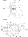
- FIG 3 shows a wideband planar balun 320, which has been found to be suitable for output capacitance compensation of PA devices.
- the planar balun 320 in this example is derived from a Marchand balun. This type of balun can be operated at 50 ohm impedance level, and can also be designed with some impedance transformation, for example 12.5 ohm differential to 50 ohm single ended, and can show a fractional bandwidth between 30-40%.
- the balun 320 shown in figure 3 has a first differential / unbalanced node 324, a second differential / unbalanced node 326, a single-ended / balanced node 328 and a reference terminal 309 such as ground.
- the balun also has two broadside-coupled lines, along with a tuning capacitor 340 at the differential end.
- a first set of broadside-coupled lines includes a first transmission line 330 and a second transmission line 332.
- the first transmission line 330 has a first end and a second end.
- the second end of the first transmission line is 330 connected to the unbalanced node 328.
- the second transmission line 332 also has a first end and a second end.
- the second transmission line 332 is capacitively and/or inductively coupled to the first transmission line 330.
- the first end of the second transmission line 332 is connected to the first balanced node 324.
- the second end of the second transmission line 332 is connected to the reference terminal 309.
- a second set of broadside-coupled lines includes a third transmission line 334 and a fourth transmission line 336.
- the third transmission line 334 has a first end and a second end. The first end of the third transmission line 334 is connected to the first end of the first transmission line 330. The second end of the third transmission line 334 is connected to the reference terminal 309.
- the fourth transmission line 336 also has a first end and a second end. The first end of the fourth transmission line 336 is connected to the second balanced node 326.
- the fourth transmission line 336 is capacitively and/or inductively coupled to the third transmission line 334.
- the second end of the fourth transmission line 336 is connected to the reference terminal 309.
- the balun 320 does not provide any impedance transformation and is equivalent to a 50 ohm transmission line in the pass band.
- this balun can be designed at any impedance level by appropriately choosing the odd-mode impedances of the broadside-coupled lines.
- Figure 4 shows an example embodiment of a wideband power amplifier cell 402.
- the power amplifier cell 402 includes a first input terminal 404 that can receive a first-balanced-input-signal, a second input terminal 406 that can receive a second-balanced-input-signal, an output terminal 408, and a reference terminal 409.
- the output terminal 408 of the power amplifier cell 402 is connected to a wideband-output-matching-circuit 478, which in turn is connected to an RF load 480.
- figure 4 also shows an input balun 450.
- the input balun 450 has an unbalanced-input-terminal, a balanced-first-output-terminal, and a balanced-second-output-terminal.
- the first-input-balun-input-terminal receives an unbalanced input signal.
- the balanced-first-output-terminal provides a signal for the first input terminal 404 of the power amplifier cell 402
- the balanced-second-output-terminal provides a signal for the second input terminal 406 of the power amplifier cell 402.
- the balanced-first-output-terminal of the input balun 450 is connected to an input terminal of a first-wideband-input-matching-circuit 452.
- An output terminal of the first-wideband-input-matching-circuit 452 is connected to the first input terminal 404 of the power amplifier cell 402 to provide the first-balanced-input-signal.
- the balanced-second-output-terminal of the input balun 450 is connected to an input terminal of a second-wideband-input-matching-circuit 454.
- An output terminal of the second-wideband-input-matching-circuit 454 is connected to the second input terminal 406 of the power amplifier cell 402 to provide the second-balanced-input-signal.
- the power amplifier cell 402 includes a first power amplifier 410 and a second power amplifier 416.
- the first power amplifier 410 has a first-PA-input-terminal 412 and a first-PA-output-terminal 414.
- the first-PA-input-terminal 412 is connected to the first input terminal 404.
- the first power amplifier 410 also has a first-PA-reference-terminal that is connected to the reference terminal 409.
- the second power amplifier 416 has a second-PA-input-terminal 418 and a second-PA-output-terminal 420.
- the second-PA-input-terminal 418 is connected to the second input terminal 406.
- the second power amplifier 416 also has a second-PA-reference-terminal that is connected to the reference terminal 409.
- each of the first power amplifier 410 and the second power amplifier 416 is implemented as a laterally diffused metal oxide semiconductor (LDMOS) field effect transistor (FET).
- LDMOS laterally diffused metal oxide semiconductor
- FET field effect transistor
- the first power amplifier 410 and the second power amplifier 416 can be any type of transistor.
- the power amplifier cell 402 also includes a balun 422 that comprises a first balanced node 424, a second balanced node 426, and an unbalanced node 428.
- the first balanced node 424 is connected to the first-PA-output-terminal 414.
- the second balanced node 426 is connected to the second-PA-output-terminal 420.
- the unbalanced node 428 is connected to the output terminal 408.
- the balun 422 also includes a first transmission line 430 and a second transmission line 432 that are capacitively and/or inductively coupled to each other.
- the first transmission line 430 has a first end and a second end. The second end of the first transmission line 430 is connected to the unbalanced node 428.
- the second transmission line 432 has a first end and a second end. The first end of the second transmission line is connected to the first balanced node 424.
- the second end of the second transmission line 432 is connected to the reference 409 terminal, in this example through an optional first-RF-decoupling-capacitor 456.
- the balun 422 also includes a third transmission line 434 and a fourth transmission line 436 that are capacitively and/or inductively coupled to each other.
- the third transmission line 434 has a first end and a second end. The first end of the third transmission line 434 is connected to the first end of the first transmission line 430. The second end of the third transmission line 434 is connected to the reference terminal 409.
- the fourth transmission line 436 has a first end and a second end. The first end of the fourth transmission line 436 is connected to the second balanced node 426. The second end of the fourth transmission line 436 is connected to the reference terminal 409, in this example through an optional second-RF-decoupling-capacitor 458.
- first transmission line 430 and the third transmission line 434 are connected in series between the unbalanced node 428 (for connecting to the RF load) and the reference terminal 409.
- a bias-node 460 is defined as the node between the series connection of the first transmission line 430 and the third transmission line 434.
- the bias-node is connected to the second end of the second transmission line 432 and the second end of the fourth transmission line 436.
- the balun also includes a biasing circuit 438 connected between (i) the reference terminal 409, and (ii) the bias-node 460.
- the biasing circuit 438 comprises a bias-voltage-source 462 and a bias-capacitor 464 connected in parallel with each other between the reference terminal 409 and the bias-node 460.
- the balun 422 also includes a tuning component 440 connected between the first balanced node 424 and the second balanced node 426.
- the tuning component 440 which may also be referred to as a shunt component, may be a capacitor or an inductor (depending on the technology of the PA devices 410, 416 and the frequency of operation).
- the tuning component 440 is used to tune the power amplifier cell 402 for adequate operation at a desired RF frequency.
- the first power amplifier 410 has an associated first-PA-output-capacitance (Cdev) 442 and the second power amplifier 416 has an associated second-PA-output-capacitance (Cdev) 444.
- the inclusion of the output capacitances represents a realistic / practical structure of an LDMOS device.
- the value of the impedance of the tuning component 440 can be selected for operation at a desired frequency band. That is, the impedance value of the tuning component 440 can be selected / designed based on the impedance values of the first-PA-output-capacitance 442 and the second-PA-output-capacitance 444.
- the balun 422 can be designed at 2 times the base-impedance of the PA devices 410, 416, which is defined by the following equation.
- R opt 0.5 V drain ⁇ V knee 2 P max
- the impedance (R opt ) represented in equation (1) is the load required by the PA devices 410, 416 to deliver maximum power, assuming that the output capacitances (the first-PA-output-capacitance 442 and the second-PA-output-capacitance 444) of the PA devices 410, 416 is not present.
- some or all of the required tuning capacitance can be replaced by the output capacitances (the first-PA-output-capacitance 442 and the second-PA-output-capacitance 444) of the PA devices 410, 416.
- the output capacitances of the PA devices 410, 416 can be compensated in a very wideband fashion, whilst retaining wideband balun operation.
- the PA devices 410, 416 can present a substantially real impedance, or at least with a smaller imaginary component than would be present if the value of the combined impedance of (i) the first-PA-output-capacitance 442, (ii) the second-PA-output-capacitance 444, and (iii) the tuning component 440 were not used. This can also provide a good Q factor.
- each of the first power amplifier 410 and the second power amplifier 416 have an optimum load parameter (R opt );
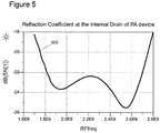
- Figure 5 illustrates an input reflection (dB) against frequency profile 500 for the power amplifier cell of figure 4 .
- the reflection coefficient at the internal drain of the PA device for optimum load (R opt ) is shown.
- the profile 500 is shown over the frequency range of 1.6 to 2.8 GHz.
- an input reflection of less than -20 dB may be required.
- the input reflection profile 500 is less than -20 dB between about 1.75 GHz and about 2.75 GHz, which can be considered as representing a device with acceptable performance across a very wide bandwidth.
- the power amplifier cell 402 in this example also shows a first-bondwire-inductance (Lb) 466 connected in series between the first-PA-output-terminal 414 and the first balanced node 424, and also a second-bondwire-inductance (Lb) 468 connected in series between the second-PA-output-terminal 420 and the second balanced node 426.
- the first-bondwire-inductance 466 and the second-bondwire-inductance 468 are used to connect the power amplifiers to the balun 422.
- balun 422 acts very much like a transmission line in the RF pass-band, and can therefore easily and conveniently be used to replace transmission line components in advanced wideband PA architectures such as ultra-wideband (UWB) Doherty amplifiers, thereby resulting in compact and wideband circuits.
- UWB Doherty made with this coupler is shown in figure 6 .
- Figure 6 shows an ultra-wideband Doherty PA 600 that uses two wideband PA cells 602a, 602b such as the one illustrated in figure 4 .
- the Doherty amplifier has a Doherty-amplifier-output-terminal 686.
- the Doherty PA 600 includes a main-PA-cell 602a, and a peak-PA-cell 602b.
- the main-wideband-PA-cell 602a includes a main-PA-first-input-terminal 604a, a main-PA-second-input-terminal 606a, and a main-PA-output-terminal 608a.
- the peak-wideband-PA-cell 602b includes a peak-PA-first-input-terminal 604b, a peak-PA-second-input-terminal 606b, and a peak-PA-output-terminal 608b.
- the Doherty PA 600 also includes an input splitter 670 having a splitter-input-terminal, a splitter-main-output-terminal 682 and a splitter-peak-output-terminal 684.
- the input splitter 670 receives an input signal.
- the splitter-main-output-terminal 682 provides a main-split-signal.
- the splitter-peak-output-terminal 684 provides a peak-split-signal.
- a phase shifter (not shown) is placed separately in front of the main-PA-cell 602a in this example such that the main-split-signal is 90° out of phase with respect to the peak-split-signal.
- the splitter-main-output-terminal 682 is connected to a main-unbalanced-input-terminal of a main-input-balun 650a.
- a main-balanced-first-output-terminal of the main-input-balun 650a is connected to an input terminal of a main-first-wideband-input-matching-circuit 652a.
- An output terminal of the main-first-wideband-input-matching-circuit 652a provides a main-first-balanced-input-signal to the main-PA-first-input-terminal 604a.
- a main-balanced-second-output-terminal of the main-input-balun 650a is connected to an input terminal of a main-second-wideband-input-matching-circuit 654a.
- An output terminal of the main-second-wideband-input-matching-circuit 654a provides a main-second-balanced-input-signal to the main-PA-second-input-terminal 606a.
- the splitter-peak-output-terminal 684 is connected to a peak-unbalanced-input-terminal of a peak-input-balun 650b.
- a peak-balanced-first-output-terminal of the peak-input-balun 650b is connected to an input terminal of a peak-first-wideband-input-matching-circuit 652b.
- An output terminal of the peak-first-wideband-input-matching-circuit 652b provides a peak-first-balanced-input-signal to the peak-PA-first-input-terminal 604b.
- a peak-balanced-second-output-terminal of the peak-input-balun 650b is connected to an input terminal of a peak-second-wideband-input-matching-circuit 654b.
- An output terminal of the peak-second-wideband-input-matching-circuit 654b provides a peak-second-balanced-input-signal to the peak-PA-second-input-terminal 606b.
- the main-PA-output-terminal 608a is connected to a first end of a main-transmission-line 676.
- a second end of the main-transmission-line 676 is connected to the Doherty-amplifier-output-terminal 686.
- the main-transmission-line 676 has an electrical length of ⁇ main such that total electrical length ( ⁇ main +phase delay of balun) equals 90° at the center frequency of the band, and has an impedance of 2xR opt(main) , (R opt(main) is the optimum impedance of the entire main-PA-cell 602a).
- the peak-PA-output-terminal 608b is connected to a first end of a peak-transmission-line 672.
- a second end of the peak-transmission-line 672 is connected to a first end of a compensating-transmission-line 674.
- a second end of the compensating-transmission-line 674 is connected to the Doherty-amplifier-output-terminal 686.
- the peak-transmission-line 672 has an electrical length of ⁇ peak such that the total phase delay in-front of the peaking device ( ⁇ peak + phase delay of balun) equals 90°, and has an impedance of 2xR opt(peak) (R opt(peak) is the optimum impedance of the entire peak-PA-cell 602b).
- the compensating-transmission-line 674 has an electrical length that provides a further 90° phase shift such that the output signal of the peak-PA-cell 602b is brought into phase with the output signal of the main-PA-cell 602a.
- the compensating-transmission-line 674 also has an impedance of 2xR opt(peak) .
- the Doherty-amplifier-output-terminal 686 is connected to an input terminal of a wideband-output-matching-circuit 678, which in turn is connected to an RF load 680.
- wideband PA cells 602a, 602b in the Doherty amplifier of figure 6 can advantageously provide a very wideband Doherty amplifier.
- the wideband cells can be used in numerous applications, including wideband PA class-B amplifiers, out-phasing amplifiers, wideband Doherty amplifiers for all frequency bands, and 3-way and 4-way Doherty amplifiers.
- the wideband PA cells of figures 4 and 6 can enable a balun to be designed with a structure that has little or no impedance transformation, with an impedance that is approximately equal to two time the base-impedance of the PA device. Also, the output capacitance of the PA devices can be used to contribute to the tuning capacitance for the balun structure. Furthermore, the transmission line-type properties of the wideband PA cells can be beneficially used to form wideband Doherty Amplifiers.
- the set of instructions/method steps described above are implemented as functional and software instructions embodied as a set of executable instructions which are effected on a computer or machine which is programmed with and controlled by said executable instructions. Such instructions are loaded for execution on a processor (such as one or more CPUs).
- processor includes microprocessors, microcontrollers, processor modules or subsystems (including one or more microprocessors or microcontrollers), or other control or computing devices.
- a processor can refer to a single component or to plural components.
- the set of instructions/methods illustrated herein and data and instructions associated therewith are stored in respective storage devices, which are implemented as one or more non-transient machine or computer-readable or computer-usable storage media or mediums.
- Such computer-readable or computer usable storage medium or media is (are) considered to be part of an article (or article of manufacture).
- An article or article of manufacture can refer to any manufactured single component or multiple components.
- the non-transient machine or computer usable media or mediums as defined herein excludes signals, but such media or mediums may be capable of receiving and processing information from signals and/or other transient mediums.
- Example embodiments of the material discussed in this specification can be implemented in whole or in part through network, computer, or data based devices and/or services. These may include cloud, internet, intranet, mobile, desktop, processor, look-up table, microcontroller, consumer equipment, infrastructure, or other enabling devices and services. As may be used herein and in the claims, the following non-exclusive definitions are provided.
- one or more instructions or steps discussed herein are automated.
- the terms automated or automatically mean controlled operation of an apparatus, system, and/or process using computers and/or mechanical/electrical devices without the necessity of human intervention, observation, effort and/or decision.
- any components said to be coupled or connected may be coupled or connected either directly or indirectly.
- additional components may be located between the two components that are said to be coupled or connected whilst still enabling the required functionality to be achieved.
Landscapes
- Engineering & Computer Science (AREA)
- Power Engineering (AREA)
- Microelectronics & Electronic Packaging (AREA)
- Amplifiers (AREA)
Claims (14)
- Cellule d'amplificateur de puissance comprenant :une première borne d'entrée configurée pour recevoir un premier signal d'entrée équilibrée ;une deuxième borne d'entrée configurée pour recevoir un deuxième signal d'entrée équilibrée ;une borne de sortie ;une borne de référence ;un premier amplificateur de puissance, PA, ayant :une première borne d'entrée PA reliée à la première borne d'entrée ; etune première borne de sortie PA ;le premier amplificateur de puissance ayant une première capacité de sortie PA associée ;un deuxième amplificateur de puissance ayant :une deuxième borne d'entrée PA reliée à la deuxième borne d'entrée ; etune deuxième borne de sortie PA ;le deuxième amplificateur de puissance ayant une deuxième capacité de sortie PA associée ;un balun comprenant :un premier nœud équilibré relié à la première borne de sortie PA ;un deuxième nœud équilibré relié à la deuxième borne de sortie PA ;un nœud déséquilibré relié à la borne de sortie ;une première ligne de transmission avec une première extrémité et une deuxième extrémité, la deuxième extrémité de la première ligne de transmission étant reliée au nœud déséquilibré ;une deuxième ligne de transmission avec une première extrémité et une deuxième extrémité, dans laquelle la deuxième ligne de transmission est couplée de manière capacitive et/ou inductive à la première ligne de transmission, la première extrémité de la deuxième ligne de transmission est reliée au premier nœud équilibré, et la deuxième extrémité de la deuxième ligne de transmission est reliée à la borne de référence ;une troisième ligne de transmission avec une première extrémité et une deuxième extrémité, dans laquelle la première extrémité de la troisième ligne de transmission est reliée à la première extrémité de la première ligne de transmission, et la deuxième extrémité de la troisième ligne de transmission est reliée à la borne de référence ;une quatrième ligne de transmission avec une première extrémité et une deuxième extrémité, dans laquelle la première extrémité de la quatrième ligne de transmission est reliée au deuxième nœud équilibré, la quatrième ligne de transmission est couplée de manière capacitive et/ou inductive à la troisième ligne de transmission, et la deuxième extrémité de la quatrième ligne de transmission est reliée à la borne de référence ; etun composant de réglage relié entre le premier nœud équilibré et le deuxième nœud équilibré ; dans laquelle une impédance combinée formée par la première capacité de sortie PA, la deuxième capacité de sortie PA et le composant de réglage étant conçue avec une valeur pour un fonctionnement à une bande de fréquences souhaitée, de sorte que les premier et deuxième amplificateurs de puissance présentent une impédance sensiblement réelle ; et dans laquelle chacun du premier amplificateur de puissance et du deuxième amplificateur de puissance a un paramètre de charge optimale (Ropt) correspondant à une charge requise par les premier et deuxième amplificateurs de puissance pour livrer une puissance maximale, en supposant que la première capacité de sortie PA et la deuxième capacité de sortie PA ne sont pas présentes ;le balun étant conçu de sorte que :
une impédance entre le premier nœud équilibré et le deuxième nœud équilibré du balun (Zdiff) est égale à une impédance (Zsingle) entre le nœud déséquilibré et la borne de référence, et est également égale à deux fois le paramètre de charge optimale (Ropt) ; l'amplificateur de puissance comprenant en outre un circuit de polarisation relié entre la borne de référence et la deuxième extrémité de la deuxième ligne de transmission et la deuxième extrémité de la quatrième ligne de transmission. - Cellule d'amplificateur de puissance selon la revendication 1, dans laquelle la deuxième extrémité de la deuxième ligne de transmission est reliée à la borne de référence par l'intermédiaire d'un premier condensateur de découplage RF, et dans laquelle la deuxième extrémité de la quatrième ligne de transmission est reliée à la borne de référence par l'intermédiaire d'un deuxième condensateur de découplage RF.
- Cellule d'amplificateur de puissance selon l'une quelconque des revendications précédentes, dans laquelle le circuit de polarisation comprend une source de tension de polarisation.
- Cellule d'amplificateur de puissance selon la revendication 3, dans laquelle le circuit de polarisation comprend la source de tension de polarisation et un condensateur de polarisation reliés l'un à l'autre en parallèle entre : (i) la borne de référence, et (ii) la deuxième extrémité de la deuxième ligne de transmission et la deuxième extrémité de la quatrième ligne de transmission.
- Cellule d'amplificateur de puissance selon l'une quelconque des revendications précédentes, dans laquelle le premier amplificateur de puissance et le deuxième amplificateur de puissance comprennent des transistors à effet de champ.
- Cellule d'amplificateur de puissance selon l'une quelconque des revendications précédentes, comprenant en outre :une première inductance de fil de liaison reliée en série entre la première borne de sortie PA et le premier nœud équilibré ; etune deuxième inductance de fil de liaison reliée en série entre la deuxième borne de sortie PA et le deuxième nœud équilibré.
- Cellule d'amplificateur de puissance selon l'une quelconque des revendications précédentes, dans laquelle le balun comprend un balun plan.
- Cellule d'amplificateur de puissance selon l'une quelconque des revendications précédentes, dans laquelle le balun comprend un balun de Marchand.
- Circuit d'amplificateur de puissance comprenant :la cellule d'amplificateur de puissance selon l'une quelconque des revendications précédentes ;un balun d'entrée ayant une borne d'entrée déséquilibrée, une première borne de sortie équilibrée, et une deuxième borne de sortie équilibrée ;dans lequel la borne d'entrée déséquilibrée est configurée pour recevoir un signal d'entrée déséquilibrée, la première borne de sortie équilibrée est configurée pour délivrer un signal pour la première borne d'entrée de la cellule d'amplificateur de puissance, et la deuxième borne de sortie équilibrée est configurée pour délivrer un signal pour la deuxième borne d'entrée de la cellule d'amplificateur de puissance.
- Circuit d'amplificateur de puissance selon la revendication 9, comprenant en outre :un premier circuit d'adaptation d'entrée de bande large ; etun deuxième circuit d'adaptation d'entrée de bande large ;dans lequel :la première borne de sortie équilibrée est reliée à une borne d'entrée du premier circuit d'adaptation d'entrée de bande large, et une borne de sortie du premier circuit d'adaptation d'entrée de bande large est reliée à la première borne d'entrée de la cellule d'amplificateur de puissance, etla deuxième borne de sortie équilibrée est reliée à une borne d'entrée du deuxième circuit d'adaptation d'entrée de bande large, et une borne de sortie du deuxième circuit d'adaptation d'entrée de bande large est reliée à la deuxième borne d'entrée de la cellule d'amplificateur de puissance.
- Amplificateur Doherty comprenant :une borne de sortie d'amplificateur Doherty ;une cellule d'amplificateur de puissance principale comprenant la cellule d'amplificateur de puissance selon l'une quelconque des revendications précédentes, la cellule d'amplificateur de puissance principale comprenant : une première borne d'entrée PA principale, une deuxième borne d'entrée PA principale, et une borne de sortie PA principale correspondant respectivement à la première borne d'entrée, la deuxième borne d'entrée et la borne de sortie de la cellule d'amplificateur de puissance ;dans lequel la borne de sortie PA principale est reliée à la borne de sortie d'amplificateur Doherty par l'intermédiaire d'une ligne de transmission principale ;une cellule d'amplificateur de puissance de pointe comprenant la cellule d'amplificateur de puissance selon l'une quelconque des revendications précédentes, la cellule de l'amplificateur de puissance de pointe comprenant : une première borne d'entrée PA de pointe, une deuxième borne d'entrée PA de pointe, et une borne de sortie PA de pointe, correspondant respectivement à la première borne d'entrée, la deuxième borne d'entrée et la borne de sortie de la cellule d'amplificateur de puissance ;dans lequel la borne de sortie PA de pointe est reliée à la borne de sortie d'amplificateur Doherty par l'intermédiaire de la liaison en série (i) d'une ligne de transmission de pointe et (ii) d'une ligne de transmission de compensation.
- Amplificateur Doherty selon la revendication 11, dans lequel une impédance caractéristique de la ligne de transmission principale, de la ligne de transmission de pointe et de la ligne de transmission de compensation est égale à deux fois le paramètre de charge optimale de la cellule d'amplificateur de puissance correspondante.
- Amplificateur Doherty selon la revendication 11 ou 12, dans lequel :la ligne de transmission principale a une longueur électrique à la fréquence centrale de la bande de fréquences souhaitée de sorte qu'une somme d'un retard de phase du balun et du déphasage introduit par la ligne de transmission principale soit égale à 90 degrés ;la ligne de transmission de pointe a une longueur électrique à la fréquence centrale de la bande de fréquences souhaitée de sorte qu'une somme d'un retard de phase du balun et du déphasage introduit par la ligne de transmission de pointe soit égale à 90 degrés ;la ligne de transmission de compensation a une longueur électrique à la fréquence centrale de la bande de fréquences souhaitée qui est égale à 90 degrés.
- Circuit intégré comprenant la cellule d'amplificateur de puissance selon l'une quelconque des revendications 1 à 8, ou le circuit d'amplificateur de puissance selon la revendication 9 ou 10, ou l'amplificateur Doherty selon la revendication 11, 12 ou 13.
Priority Applications (3)
| Application Number | Priority Date | Filing Date | Title |
|---|---|---|---|
| EP15185534.3A EP3145077B1 (fr) | 2015-09-16 | 2015-09-16 | Cellule d'amplificateur de puissance |
| US15/267,904 US9768736B2 (en) | 2015-09-16 | 2016-09-16 | Power amplifier cell |
| CN201610833675.3A CN106992758B (zh) | 2015-09-16 | 2016-09-19 | 功率放大器单元 |
Applications Claiming Priority (1)
| Application Number | Priority Date | Filing Date | Title |
|---|---|---|---|
| EP15185534.3A EP3145077B1 (fr) | 2015-09-16 | 2015-09-16 | Cellule d'amplificateur de puissance |
Publications (2)
| Publication Number | Publication Date |
|---|---|
| EP3145077A1 EP3145077A1 (fr) | 2017-03-22 |
| EP3145077B1 true EP3145077B1 (fr) | 2019-11-13 |
Family
ID=54148398
Family Applications (1)
| Application Number | Title | Priority Date | Filing Date |
|---|---|---|---|
| EP15185534.3A Active EP3145077B1 (fr) | 2015-09-16 | 2015-09-16 | Cellule d'amplificateur de puissance |
Country Status (3)
| Country | Link |
|---|---|
| US (1) | US9768736B2 (fr) |
| EP (1) | EP3145077B1 (fr) |
| CN (1) | CN106992758B (fr) |
Families Citing this family (17)
| Publication number | Priority date | Publication date | Assignee | Title |
|---|---|---|---|---|
| CN107046408B (zh) * | 2017-04-14 | 2020-09-18 | 上海华虹宏力半导体制造有限公司 | 一种低成本射频差分放大器 |
| EP3477859B1 (fr) * | 2017-10-31 | 2020-09-30 | Nxp B.V. | Cellule d'amplificateur de puissance |
| US10826457B2 (en) * | 2018-02-07 | 2020-11-03 | Swiftlink Technologies Inc. | Broadband power amplifier and matching network for multi-band millimeter-wave 5G communication |
| CN110417356B (zh) * | 2018-04-26 | 2023-07-21 | 苏州远创达科技有限公司 | 一种宽带高效率多赫蒂放大器 |
| EP3855619B1 (fr) | 2018-11-30 | 2024-07-31 | Huawei Technologies Co., Ltd. | Circuit amplificateur de puissance |
| US10911016B2 (en) | 2019-01-08 | 2021-02-02 | Analog Devices, Inc. | Wideband balun |
| US11101227B2 (en) | 2019-07-17 | 2021-08-24 | Analog Devices International Unlimited Company | Coupled line structures for wideband applications |
| SE2050563A1 (en) | 2020-05-13 | 2021-07-13 | Syntronic Ab | A bias circuit for a Doherty amplifier, and a wireless communication system |
| US12199585B2 (en) | 2020-12-10 | 2025-01-14 | Skyworks Solutions, Inc. | Baluns with integrated matching networks |
| JP2022112751A (ja) * | 2021-01-22 | 2022-08-03 | 株式会社村田製作所 | 合成バラン及び差動増幅装置 |
| CN115622518B (zh) * | 2021-06-30 | 2024-08-23 | 锐石创芯(深圳)科技股份有限公司 | 一种推挽功率放大电路及射频前端模组 |
| JP7651996B2 (ja) * | 2021-07-20 | 2025-03-27 | 住友電気工業株式会社 | アウトフェージング増幅器 |
| US20240048107A1 (en) * | 2022-08-05 | 2024-02-08 | Samsung Electronics Co., Ltd. | Output matching network with improved wide band characteristics and power amplifier network including the same |
| CN115940839A (zh) * | 2022-12-08 | 2023-04-07 | 康希通信科技(上海)有限公司 | 放大电路、无线通信模块和电子设备 |
| CN117353694B (zh) * | 2023-12-04 | 2024-03-08 | 宜确半导体(苏州)有限公司 | 一种差分阻抗变换器及电子设备 |
| US20250379548A1 (en) * | 2024-06-05 | 2025-12-11 | Qualcomm Incorporated | Coupler-based mm-wave doherty power amplifier |
| CN119154809A (zh) * | 2024-09-04 | 2024-12-17 | 北京昂瑞微电子技术股份有限公司 | 基于多赫蒂放大器的射频功率放大电路 |
Family Cites Families (11)
| Publication number | Priority date | Publication date | Assignee | Title |
|---|---|---|---|---|
| FR2696887B1 (fr) * | 1992-10-09 | 1994-11-18 | Thomson Lgt | Amplificateur de puissance large bande haute fréquence. |
| US6133788A (en) * | 1998-04-02 | 2000-10-17 | Ericsson Inc. | Hybrid Chireix/Doherty amplifiers and methods |
| US6311046B1 (en) * | 1998-04-02 | 2001-10-30 | Ericsson Inc. | Linear amplification systems and methods using more than two constant length vectors |
| US20060284698A1 (en) * | 2005-06-15 | 2006-12-21 | Nokia Corporation | Low-loss microstrip transmission line structure and a method for its implementation |
| US7961048B2 (en) * | 2008-12-12 | 2011-06-14 | Samsung Electro-Mechanics Company | Integrated power amplifiers for use in wireless communication devices |
| EP2339745A1 (fr) * | 2009-12-15 | 2011-06-29 | Nxp B.V. | Amplificateur de Doherty |
| US8410853B2 (en) * | 2010-06-01 | 2013-04-02 | Nxp B.V. | Inductive circuit arrangement |
| US8576010B2 (en) * | 2010-10-19 | 2013-11-05 | Samsung Electronics Co., Ltd. | Apparatus and method for a switched capacitor architecture for multi-band doherty power amplifiers |
| EP2621084A1 (fr) * | 2012-01-24 | 2013-07-31 | System Engineering Solutions S.r.l. | Amplificateur de puissance à topologie Doherty modifiée |
| CN104218897A (zh) * | 2013-05-31 | 2014-12-17 | 诺基亚公司 | 高效紧凑Doherty功率放大器装置和方法 |
| EP2899803B1 (fr) * | 2014-01-24 | 2020-06-24 | Ampleon Netherlands B.V. | Circuit comprenant un symétriseur et des éléments de transformation d'impédance |
-
2015
- 2015-09-16 EP EP15185534.3A patent/EP3145077B1/fr active Active
-
2016
- 2016-09-16 US US15/267,904 patent/US9768736B2/en active Active
- 2016-09-19 CN CN201610833675.3A patent/CN106992758B/zh active Active
Non-Patent Citations (1)
| Title |
|---|
| None * |
Also Published As
| Publication number | Publication date |
|---|---|
| US9768736B2 (en) | 2017-09-19 |
| CN106992758A (zh) | 2017-07-28 |
| EP3145077A1 (fr) | 2017-03-22 |
| CN106992758B (zh) | 2022-01-07 |
| US20170077873A1 (en) | 2017-03-16 |
Similar Documents
| Publication | Publication Date | Title |
|---|---|---|
| EP3145077B1 (fr) | Cellule d'amplificateur de puissance | |
| US10594274B2 (en) | Power amplifier cell | |
| EP3093987B1 (fr) | Correction de phase dans un amplificateur de puissance de type doherty | |
| US10218313B2 (en) | Amplifier assembly | |
| US10050588B2 (en) | Doherty amplifier circuits | |
| CN108462477B (zh) | 功率放大电路 | |
| US12155352B2 (en) | Power amplifier arrangement | |
| US8368465B2 (en) | Power amplification apparatus | |
| CN106656069A (zh) | 一种应用于gsm射频功率放大器的多频输出匹配网络 | |
| EP2883306B1 (fr) | Dispositif pour temps de propagation de groupe négatif | |
| US10090810B2 (en) | Doherty amplifiers | |
| Kaymaksut et al. | E-band transformer-based Doherty power amplifier in 40 nm CMOS | |
| CN104218897A (zh) | 高效紧凑Doherty功率放大器装置和方法 | |
| EP2879291A1 (fr) | Amplificateur de puissance à large bande avec modulation de charge active | |
| JP2018074320A (ja) | ドハティ型増幅器 | |
| JP2008125044A (ja) | 増幅器 | |
| Wang et al. | A compact SiGe amplifier-frequency-doubler chain with 7.1-dBm p sat and 98-GHz bandwidth for sub-THz applications | |
| EP3570433B1 (fr) | Amplificateur de doherty | |
| EP2928074B1 (fr) | Amplificateur à large bande | |
| EP3771096A1 (fr) | Amplificateur | |
| CN109687828B (zh) | 一种射频功率放大器及基站 | |
| US8749311B2 (en) | Active antenna arrangement with Doherty amplifier | |
| CN219041744U (zh) | 放大电路、无线通信模块和电子设备 | |
| Wu et al. | A 87.5–104.4 GHz Broadband Power amplifier with RF switch using Transmission line connected in parallel with MCR Transformer in 130 nm SiGe BiCMOS | |
| CN108736122B (zh) | 一种合路装置、Doherty放大器及基站 |
Legal Events
| Date | Code | Title | Description |
|---|---|---|---|
| PUAI | Public reference made under article 153(3) epc to a published international application that has entered the european phase |
Free format text: ORIGINAL CODE: 0009012 |
|
| STAA | Information on the status of an ep patent application or granted ep patent |
Free format text: STATUS: THE APPLICATION HAS BEEN PUBLISHED |
|
| AK | Designated contracting states |
Kind code of ref document: A1 Designated state(s): AL AT BE BG CH CY CZ DE DK EE ES FI FR GB GR HR HU IE IS IT LI LT LU LV MC MK MT NL NO PL PT RO RS SE SI SK SM TR |
|
| AX | Request for extension of the european patent |
Extension state: BA ME |
|
| STAA | Information on the status of an ep patent application or granted ep patent |
Free format text: STATUS: REQUEST FOR EXAMINATION WAS MADE |
|
| 17P | Request for examination filed |
Effective date: 20170920 |
|
| RBV | Designated contracting states (corrected) |
Designated state(s): AL AT BE BG CH CY CZ DE DK EE ES FI FR GB GR HR HU IE IS IT LI LT LU LV MC MK MT NL NO PL PT RO RS SE SI SK SM TR |
|
| GRAP | Despatch of communication of intention to grant a patent |
Free format text: ORIGINAL CODE: EPIDOSNIGR1 |
|
| STAA | Information on the status of an ep patent application or granted ep patent |
Free format text: STATUS: GRANT OF PATENT IS INTENDED |
|
| RIC1 | Information provided on ipc code assigned before grant |
Ipc: H03F 3/195 20060101ALI20190517BHEP Ipc: H03F 3/26 20060101ALI20190517BHEP Ipc: H03F 3/213 20060101ALI20190517BHEP Ipc: H03F 1/02 20060101AFI20190517BHEP Ipc: H03F 1/56 20060101ALI20190517BHEP Ipc: H01P 5/10 20060101ALI20190517BHEP Ipc: H03F 3/60 20060101ALI20190517BHEP Ipc: H03H 7/38 20060101ALI20190517BHEP Ipc: H03H 7/42 20060101ALI20190517BHEP |
|
| INTG | Intention to grant announced |
Effective date: 20190614 |
|
| GRAS | Grant fee paid |
Free format text: ORIGINAL CODE: EPIDOSNIGR3 |
|
| GRAA | (expected) grant |
Free format text: ORIGINAL CODE: 0009210 |
|
| STAA | Information on the status of an ep patent application or granted ep patent |
Free format text: STATUS: THE PATENT HAS BEEN GRANTED |
|
| AK | Designated contracting states |
Kind code of ref document: B1 Designated state(s): AL AT BE BG CH CY CZ DE DK EE ES FI FR GB GR HR HU IE IS IT LI LT LU LV MC MK MT NL NO PL PT RO RS SE SI SK SM TR |
|
| REG | Reference to a national code |
Ref country code: CH Ref legal event code: EP Ref country code: AT Ref legal event code: REF Ref document number: 1202729 Country of ref document: AT Kind code of ref document: T Effective date: 20191115 |
|
| REG | Reference to a national code |
Ref country code: DE Ref legal event code: R096 Ref document number: 602015041530 Country of ref document: DE |
|
| REG | Reference to a national code |
Ref country code: IE Ref legal event code: FG4D |
|
| REG | Reference to a national code |
Ref country code: NL Ref legal event code: FP |
|
| REG | Reference to a national code |
Ref country code: LT Ref legal event code: MG4D |
|
| PG25 | Lapsed in a contracting state [announced via postgrant information from national office to epo] |
Ref country code: PT Free format text: LAPSE BECAUSE OF FAILURE TO SUBMIT A TRANSLATION OF THE DESCRIPTION OR TO PAY THE FEE WITHIN THE PRESCRIBED TIME-LIMIT Effective date: 20200313 Ref country code: NO Free format text: LAPSE BECAUSE OF FAILURE TO SUBMIT A TRANSLATION OF THE DESCRIPTION OR TO PAY THE FEE WITHIN THE PRESCRIBED TIME-LIMIT Effective date: 20200213 Ref country code: BG Free format text: LAPSE BECAUSE OF FAILURE TO SUBMIT A TRANSLATION OF THE DESCRIPTION OR TO PAY THE FEE WITHIN THE PRESCRIBED TIME-LIMIT Effective date: 20200213 Ref country code: FI Free format text: LAPSE BECAUSE OF FAILURE TO SUBMIT A TRANSLATION OF THE DESCRIPTION OR TO PAY THE FEE WITHIN THE PRESCRIBED TIME-LIMIT Effective date: 20191113 Ref country code: LT Free format text: LAPSE BECAUSE OF FAILURE TO SUBMIT A TRANSLATION OF THE DESCRIPTION OR TO PAY THE FEE WITHIN THE PRESCRIBED TIME-LIMIT Effective date: 20191113 Ref country code: PL Free format text: LAPSE BECAUSE OF FAILURE TO SUBMIT A TRANSLATION OF THE DESCRIPTION OR TO PAY THE FEE WITHIN THE PRESCRIBED TIME-LIMIT Effective date: 20191113 Ref country code: GR Free format text: LAPSE BECAUSE OF FAILURE TO SUBMIT A TRANSLATION OF THE DESCRIPTION OR TO PAY THE FEE WITHIN THE PRESCRIBED TIME-LIMIT Effective date: 20200214 Ref country code: SE Free format text: LAPSE BECAUSE OF FAILURE TO SUBMIT A TRANSLATION OF THE DESCRIPTION OR TO PAY THE FEE WITHIN THE PRESCRIBED TIME-LIMIT Effective date: 20191113 Ref country code: LV Free format text: LAPSE BECAUSE OF FAILURE TO SUBMIT A TRANSLATION OF THE DESCRIPTION OR TO PAY THE FEE WITHIN THE PRESCRIBED TIME-LIMIT Effective date: 20191113 |
|
| PG25 | Lapsed in a contracting state [announced via postgrant information from national office to epo] |
Ref country code: RS Free format text: LAPSE BECAUSE OF FAILURE TO SUBMIT A TRANSLATION OF THE DESCRIPTION OR TO PAY THE FEE WITHIN THE PRESCRIBED TIME-LIMIT Effective date: 20191113 Ref country code: IS Free format text: LAPSE BECAUSE OF FAILURE TO SUBMIT A TRANSLATION OF THE DESCRIPTION OR TO PAY THE FEE WITHIN THE PRESCRIBED TIME-LIMIT Effective date: 20200313 Ref country code: HR Free format text: LAPSE BECAUSE OF FAILURE TO SUBMIT A TRANSLATION OF THE DESCRIPTION OR TO PAY THE FEE WITHIN THE PRESCRIBED TIME-LIMIT Effective date: 20191113 |
|
| PG25 | Lapsed in a contracting state [announced via postgrant information from national office to epo] |
Ref country code: AL Free format text: LAPSE BECAUSE OF FAILURE TO SUBMIT A TRANSLATION OF THE DESCRIPTION OR TO PAY THE FEE WITHIN THE PRESCRIBED TIME-LIMIT Effective date: 20191113 |
|
| PG25 | Lapsed in a contracting state [announced via postgrant information from national office to epo] |
Ref country code: ES Free format text: LAPSE BECAUSE OF FAILURE TO SUBMIT A TRANSLATION OF THE DESCRIPTION OR TO PAY THE FEE WITHIN THE PRESCRIBED TIME-LIMIT Effective date: 20191113 Ref country code: CZ Free format text: LAPSE BECAUSE OF FAILURE TO SUBMIT A TRANSLATION OF THE DESCRIPTION OR TO PAY THE FEE WITHIN THE PRESCRIBED TIME-LIMIT Effective date: 20191113 Ref country code: DK Free format text: LAPSE BECAUSE OF FAILURE TO SUBMIT A TRANSLATION OF THE DESCRIPTION OR TO PAY THE FEE WITHIN THE PRESCRIBED TIME-LIMIT Effective date: 20191113 Ref country code: RO Free format text: LAPSE BECAUSE OF FAILURE TO SUBMIT A TRANSLATION OF THE DESCRIPTION OR TO PAY THE FEE WITHIN THE PRESCRIBED TIME-LIMIT Effective date: 20191113 Ref country code: EE Free format text: LAPSE BECAUSE OF FAILURE TO SUBMIT A TRANSLATION OF THE DESCRIPTION OR TO PAY THE FEE WITHIN THE PRESCRIBED TIME-LIMIT Effective date: 20191113 |
|
| REG | Reference to a national code |
Ref country code: DE Ref legal event code: R097 Ref document number: 602015041530 Country of ref document: DE |
|
| REG | Reference to a national code |
Ref country code: AT Ref legal event code: MK05 Ref document number: 1202729 Country of ref document: AT Kind code of ref document: T Effective date: 20191113 |
|
| PG25 | Lapsed in a contracting state [announced via postgrant information from national office to epo] |
Ref country code: SM Free format text: LAPSE BECAUSE OF FAILURE TO SUBMIT A TRANSLATION OF THE DESCRIPTION OR TO PAY THE FEE WITHIN THE PRESCRIBED TIME-LIMIT Effective date: 20191113 Ref country code: SK Free format text: LAPSE BECAUSE OF FAILURE TO SUBMIT A TRANSLATION OF THE DESCRIPTION OR TO PAY THE FEE WITHIN THE PRESCRIBED TIME-LIMIT Effective date: 20191113 |
|
| PLBE | No opposition filed within time limit |
Free format text: ORIGINAL CODE: 0009261 |
|
| STAA | Information on the status of an ep patent application or granted ep patent |
Free format text: STATUS: NO OPPOSITION FILED WITHIN TIME LIMIT |
|
| 26N | No opposition filed |
Effective date: 20200814 |
|
| PG25 | Lapsed in a contracting state [announced via postgrant information from national office to epo] |
Ref country code: SI Free format text: LAPSE BECAUSE OF FAILURE TO SUBMIT A TRANSLATION OF THE DESCRIPTION OR TO PAY THE FEE WITHIN THE PRESCRIBED TIME-LIMIT Effective date: 20191113 Ref country code: AT Free format text: LAPSE BECAUSE OF FAILURE TO SUBMIT A TRANSLATION OF THE DESCRIPTION OR TO PAY THE FEE WITHIN THE PRESCRIBED TIME-LIMIT Effective date: 20191113 |
|
| PG25 | Lapsed in a contracting state [announced via postgrant information from national office to epo] |
Ref country code: IT Free format text: LAPSE BECAUSE OF FAILURE TO SUBMIT A TRANSLATION OF THE DESCRIPTION OR TO PAY THE FEE WITHIN THE PRESCRIBED TIME-LIMIT Effective date: 20191113 |
|
| PG25 | Lapsed in a contracting state [announced via postgrant information from national office to epo] |
Ref country code: MC Free format text: LAPSE BECAUSE OF FAILURE TO SUBMIT A TRANSLATION OF THE DESCRIPTION OR TO PAY THE FEE WITHIN THE PRESCRIBED TIME-LIMIT Effective date: 20191113 |
|
| REG | Reference to a national code |
Ref country code: CH Ref legal event code: PL |
|
| REG | Reference to a national code |
Ref country code: BE Ref legal event code: MM Effective date: 20200930 |
|
| PG25 | Lapsed in a contracting state [announced via postgrant information from national office to epo] |
Ref country code: LU Free format text: LAPSE BECAUSE OF NON-PAYMENT OF DUE FEES Effective date: 20200916 |
|
| PG25 | Lapsed in a contracting state [announced via postgrant information from national office to epo] |
Ref country code: LI Free format text: LAPSE BECAUSE OF NON-PAYMENT OF DUE FEES Effective date: 20200930 Ref country code: BE Free format text: LAPSE BECAUSE OF NON-PAYMENT OF DUE FEES Effective date: 20200930 Ref country code: CH Free format text: LAPSE BECAUSE OF NON-PAYMENT OF DUE FEES Effective date: 20200930 |
|
| PG25 | Lapsed in a contracting state [announced via postgrant information from national office to epo] |
Ref country code: TR Free format text: LAPSE BECAUSE OF FAILURE TO SUBMIT A TRANSLATION OF THE DESCRIPTION OR TO PAY THE FEE WITHIN THE PRESCRIBED TIME-LIMIT Effective date: 20191113 Ref country code: MT Free format text: LAPSE BECAUSE OF FAILURE TO SUBMIT A TRANSLATION OF THE DESCRIPTION OR TO PAY THE FEE WITHIN THE PRESCRIBED TIME-LIMIT Effective date: 20191113 Ref country code: CY Free format text: LAPSE BECAUSE OF FAILURE TO SUBMIT A TRANSLATION OF THE DESCRIPTION OR TO PAY THE FEE WITHIN THE PRESCRIBED TIME-LIMIT Effective date: 20191113 |
|
| PG25 | Lapsed in a contracting state [announced via postgrant information from national office to epo] |
Ref country code: MK Free format text: LAPSE BECAUSE OF FAILURE TO SUBMIT A TRANSLATION OF THE DESCRIPTION OR TO PAY THE FEE WITHIN THE PRESCRIBED TIME-LIMIT Effective date: 20191113 |
|
| P01 | Opt-out of the competence of the unified patent court (upc) registered |
Effective date: 20230526 |
|
| PGFP | Annual fee paid to national office [announced via postgrant information from national office to epo] |
Ref country code: NL Payment date: 20230926 Year of fee payment: 9 Ref country code: IE Payment date: 20230927 Year of fee payment: 9 Ref country code: GB Payment date: 20230927 Year of fee payment: 9 |
|
| PGFP | Annual fee paid to national office [announced via postgrant information from national office to epo] |
Ref country code: FR Payment date: 20230925 Year of fee payment: 9 |
|
| REG | Reference to a national code |
Ref country code: NL Ref legal event code: MM Effective date: 20241001 |
|
| GBPC | Gb: european patent ceased through non-payment of renewal fee |
Effective date: 20240916 |
|
| PG25 | Lapsed in a contracting state [announced via postgrant information from national office to epo] |
Ref country code: NL Free format text: LAPSE BECAUSE OF NON-PAYMENT OF DUE FEES Effective date: 20241001 |
|
| PG25 | Lapsed in a contracting state [announced via postgrant information from national office to epo] |
Ref country code: GB Free format text: LAPSE BECAUSE OF NON-PAYMENT OF DUE FEES Effective date: 20240916 |
|
| PG25 | Lapsed in a contracting state [announced via postgrant information from national office to epo] |
Ref country code: FR Free format text: LAPSE BECAUSE OF NON-PAYMENT OF DUE FEES Effective date: 20240930 |
|
| PG25 | Lapsed in a contracting state [announced via postgrant information from national office to epo] |
Ref country code: IE Free format text: LAPSE BECAUSE OF NON-PAYMENT OF DUE FEES Effective date: 20240916 |
|
| PGFP | Annual fee paid to national office [announced via postgrant information from national office to epo] |
Ref country code: DE Payment date: 20250919 Year of fee payment: 11 |