EP3146632B1 - Digitale phasenregelschleifenschaltung mit filterung mit endlicher impulsantwort zur reduzierung von aliasing von quantisierungsrauschen - Google Patents
Digitale phasenregelschleifenschaltung mit filterung mit endlicher impulsantwort zur reduzierung von aliasing von quantisierungsrauschen Download PDFInfo
- Publication number
- EP3146632B1 EP3146632B1 EP15724255.3A EP15724255A EP3146632B1 EP 3146632 B1 EP3146632 B1 EP 3146632B1 EP 15724255 A EP15724255 A EP 15724255A EP 3146632 B1 EP3146632 B1 EP 3146632B1
- Authority
- EP
- European Patent Office
- Prior art keywords
- frequency
- signal
- output
- digital
- control signal
- Prior art date
- Legal status (The legal status is an assumption and is not a legal conclusion. Google has not performed a legal analysis and makes no representation as to the accuracy of the status listed.)
- Active
Links
Images



Classifications
-
- H—ELECTRICITY
- H03—ELECTRONIC CIRCUITRY
- H03L—AUTOMATIC CONTROL, STARTING, SYNCHRONISATION OR STABILISATION OF GENERATORS OF ELECTRONIC OSCILLATIONS OR PULSES
- H03L7/00—Automatic control of frequency or phase; Synchronisation
- H03L7/06—Automatic control of frequency or phase; Synchronisation using a reference signal applied to a frequency- or phase-locked loop
- H03L7/08—Details of the phase-locked loop
- H03L7/085—Details of the phase-locked loop concerning mainly the frequency- or phase-detection arrangement including the filtering or amplification of its output signal
- H03L7/093—Details of the phase-locked loop concerning mainly the frequency- or phase-detection arrangement including the filtering or amplification of its output signal using special filtering or amplification characteristics in the loop
-
- H—ELECTRICITY
- H03—ELECTRONIC CIRCUITRY
- H03L—AUTOMATIC CONTROL, STARTING, SYNCHRONISATION OR STABILISATION OF GENERATORS OF ELECTRONIC OSCILLATIONS OR PULSES
- H03L7/00—Automatic control of frequency or phase; Synchronisation
- H03L7/06—Automatic control of frequency or phase; Synchronisation using a reference signal applied to a frequency- or phase-locked loop
- H03L7/08—Details of the phase-locked loop
- H03L7/099—Details of the phase-locked loop concerning mainly the controlled oscillator of the loop
-
- H—ELECTRICITY
- H03—ELECTRONIC CIRCUITRY
- H03L—AUTOMATIC CONTROL, STARTING, SYNCHRONISATION OR STABILISATION OF GENERATORS OF ELECTRONIC OSCILLATIONS OR PULSES
- H03L7/00—Automatic control of frequency or phase; Synchronisation
- H03L7/06—Automatic control of frequency or phase; Synchronisation using a reference signal applied to a frequency- or phase-locked loop
- H03L7/16—Indirect frequency synthesis, i.e. generating a desired one of a number of predetermined frequencies using a frequency- or phase-locked loop
- H03L7/18—Indirect frequency synthesis, i.e. generating a desired one of a number of predetermined frequencies using a frequency- or phase-locked loop using a frequency divider or counter in the loop
- H03L7/197—Indirect frequency synthesis, i.e. generating a desired one of a number of predetermined frequencies using a frequency- or phase-locked loop using a frequency divider or counter in the loop a time difference being used for locking the loop, the counter counting between numbers which are variable in time or the frequency divider dividing by a factor variable in time, e.g. for obtaining fractional frequency division
- H03L7/1974—Indirect frequency synthesis, i.e. generating a desired one of a number of predetermined frequencies using a frequency- or phase-locked loop using a frequency divider or counter in the loop a time difference being used for locking the loop, the counter counting between numbers which are variable in time or the frequency divider dividing by a factor variable in time, e.g. for obtaining fractional frequency division for fractional frequency division
- H03L7/1976—Indirect frequency synthesis, i.e. generating a desired one of a number of predetermined frequencies using a frequency- or phase-locked loop using a frequency divider or counter in the loop a time difference being used for locking the loop, the counter counting between numbers which are variable in time or the frequency divider dividing by a factor variable in time, e.g. for obtaining fractional frequency division for fractional frequency division using a phase accumulator for controlling the counter or frequency divider
Definitions
- This disclosure relates generally to the field of electronic circuits, and, more particularly, to phase lock loop circuits.
- Phase lock loop circuits are electronic control circuits that are widely employed in radio, telecommunications, computers and other electronic applications.
- a few common applications of PLLs include signal demodulation, signal recovery from a noisy channel, generation of a stable frequency at multiples of an input frequency (frequency synthesis), and distribution of precisely timed clock pulses in digital logic circuits such as microprocessors. Since a single integrated circuit can provide a complete phase-locked-loop building block, the technique is widely used in modern electronic devices. These circuits can produce output frequencies from a fraction of a hertz up to many gigahertz.
- FIG. 6 depicts an arrangement of functional units in a prior art digital PLL 600 that is configured to generate a higher frequency output signal with reference to a lower frequency input signal.
- the PLL 600 includes phase detector/phase frequency detector 608, a low-pass loop filter 612, voltage controlled oscillator (VCO) 616 and a frequency divider 620.
- An external frequency generator produces a reference input signal 604 that is applied to an input of the phase detector 608.
- the output of the phase detector passes through a loop filter 612 and the filtered output operates the VCO 616.
- the VCO 616 accepts an analog control signal in the PLL circuit 600.
- a digital to analog converter (DAC) 614 generates an analog signal corresponding to a digital output signal from the loop filter 612.
- DAC digital to analog converter
- a sigma-delta modulator 613 receives the filtered digital control signal from the loop filter 612 and generates a high frequency dithered control signal output for the input of the DAC 614.
- the VCO 616 generates an output signal 640, which is passed to a frequency divider 620 and the output of the frequency divider 620 provides feedback to the phase detector 608.
- the phase detector 608 is a multiplier that produces a product of two signals to downconvert an input signal to another signal with low frequency that is close to DC.
- the VCO 616 is tuned to a range of frequencies corresponding to the higher frequency harmonic so the output of the PLL 640 is a higher frequency multiple of the input reference signal 604.
- the phase detector 608 identifies differences in phase between the input reference signal 604 and the output of the PLL 600. In situations where the PLL 600 is generating a multiplied frequency output, the higher frequency output signal 640 would not correspond to the lower-frequency input signal 604.
- the frequency divider 620 receives the higher frequency output 640 and generates a lower frequency output at the same frequency as the input reference signal 604 for the phase detector 608.
- the phase detector 608 identifies deviations between the phase of the output signal from the frequency divider 620 and the input reference signal 604. If the input reference signal and feedback signal are locked in phase, then the two signals are orthogonal to one another (separated by 90°).
- the phase detector 608 generates a corrected output signal in response to any errors between the phases of the input and output signals.
- the PLL circuit uses a negative feedback loop to correct phase differences between the input reference signal and an output signal.
- the DAC 614 In the PLL circuit 600, the DAC 614 generates an analog output that controls the VCO 616 to generate a signal for the feedback divider 620.
- the DAC 614 is a sigma-delta modulator that generates an analog version of the digital control signal from the loop filter 612.
- the DAC 614 can generate a comparatively limited number of distinct output levels, which is typically expressed as 2 M levels for a DAC with M bits of resolution. For example, a 4-bit DAC generates 16 distinct output levels.
- control of the VCO 616 requires greater precision than 16 control levels, so the DAC 614 receives a digital control signal that switches between different digital values at a high frequency to enable the DAC 614 to generate the analog control signal at average levels that are between the limited number of discrete output levels for the DAC 614.
- This high frequency operation of the DAC 614 in response to the dither signal from the sigma-delta modulator 613 is known as dithered operation.
- the output from DAC 614 changes between distinct output levels in response to the dithered digital control signal from the from the sigma-delta modulator 613.
- the sigma-delta modulator 612 dithers the digital control signal from the loop filter 612 at a high frequency, such as 1/4 th the frequency of the output signal from the VCO 616, and the DAC 614 switches output levels rapidly with reference to the dithered control signal.
- the rapid switching between output levels for the output of the DAC 614 produces a range of control signals that include intermediate values between the comparatively limited number of discrete output levels for the DAC 614, and enables detailed control of the VCO 616.
- the dithering process generates quantization noise in the control signal that is applied to the VCO 616. Since the dithering of the output from the DAC 614 occurs at a high frequency, the dithering noise has minimal negative impact on the control signal for the VCO 616, which typically has a low frequency band that includes 0 Hz (DC).
- the feedback divider 620 shifts the quantization noise from the DAC 614 down to lower frequencies that potentially interfere with the operation of the PLL because the feedback divider 620 suffers from aliasing while sampling the output signal from the VCO 616.
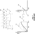
- FIG. 7 depicts the low frequency noise in more detail.
- the timing diagram 704 depicts an ideal high-frequency output signal from the VCO 616 that is provided as input to the divider 620.
- the timing diagram 708 depicts an actual output from the VCO 616 that includes quantization noise components from the DAC 614.
- the quantization noise manifests as jitter in the periods and phase of the high-frequency output signal 708.
- the divider 620 usually samples the noisy output signal 708 at a frequency lower than the DAC frequency to generate a lower-frequency divider output signal 712. For example, in FIG. 7 the divider 620 samples the noisy signal 712 at 1/4 th the frequency of the output signal from the VCO 616 in the PLL circuit. Due to aliasing that occurs when sampling at 1/4 th of the frequency of the output signal from the VCO 616, the divider 620 aliases the quantization noise in the high-frequency signal 708 in the lower-frequency feedback signal 712.
- the quantization phase noise at the high-frequency output of the VCO 616 mostly occurs at high-frequencies with low quantization noise levels near 0 Hz (DC).
- the operation of the divider 620 shifts or "folds back" the quantization noise to lower-frequencies.
- the graph 728 depicts large portions of the quantization noise around 1 ⁇ 4 and 1 ⁇ 2 of the frequency f clk from the VCO 616 are shifted down to the f clk /8 frequency to increase the DC quantization noise level 732 at that range.
- one method to reduce the effects of the quantization noise in the divider is to reduce the gain of the VCO 616.
- reducing the gain of the VCO 616 also makes the PLL circuit 600 less effective at maintaining a lock on the reference signal in the presence of drift and other variations in the reference signal. Consequently, improvements to PLL circuits that reduce low-frequency quantization noise would be beneficial.
- Document US 2012/280731 A1 discloses a phase-locked-loop that includes a phase/frequency detector, a digital filter, a digital low-pass filter, a digitally controlled oscillator and a frequency divider.
- Document "A latency-proof quantization noise reduction method for digitally-controlled ring oscillators” by Chengwen Liu discloses a quantization noise reduction method for ⁇ based digitally-controlled ring oscillators (DCRO).
- Document "A low-cost, leakage-insensitive semi-digital PLL with linear phase detection and FIR-embedded digital frequency acquisition” by Rui He discloses semi-digital PLL utilizing a hybrid DCO.
- Document WO 2008/2008/05853 A2 discloses a digital audio system including a digital phase-locked-loop circuit for generating a pulse- width-modulation clock signal.
- the present invention provides a phase-locked loop circuit with the features of claim 1.
- FIG. 1 depicts a digital PLL circuit 100.
- the digital PLL 100 includes a phase detector 108, loop filter 112, a sigma-delta modulator 114, a multi-tap finite impulse response (FIR) filter 116, an array of digital to analog converters (DACs) 118, a voltage controlled oscillator (VCO) 120, a DAC divider 124, and a feedback divider 122.
- the PLL 100 receives an input reference signal from a reference signal generator 104.
- the phase detector 108 includes two inputs that receive the reference signal and an output of the divider 122 for negative feedback. If the phases from the reference signal and the feedback signal from the divider 122 are not orthogonal to one another (e.g. separated by 90°), then the phase detector 108 generates a digital control signal to adjust the operation of the VCO 120 to correct the phase error.
- the loop filter 112 filters the digital control signal from the phase detector 108 to generate a digital filtered control signal.
- the multi-tap FIR filter 116 receives the dithered digital control signal from an output of the sigma-delta modulator 114.
- the sigma-delta modulator 114 generates the dithered control signal with reference to the control signal from the output of the loop filter 112 and with reference to a randomized high frequency signal (e.g. 1/4 th the frequency of the VCO output signal 120). While the embodiment of the PLL circuit 100 includes the sigma-delta modulator 114 to generate the dithered digital control signal, alternative embodiments include any suitable modulator embodiment that dithers the digital control signal at high frequencies.
- the dither signal enables the DAC array 118 to switch between discrete output levels to provide an average control signal to the VCO 120 that more closely approximates an analog control signal.
- the digital filtered control signal includes artifacts of the quantization error from the digital reference signal.
- the FIR filter 116 includes two or more taps that each correspond to two or more notches in the frequency band for the digital filtered signal that the DAC array 118 receives. As described in more detail below, the notches are centered on the frequencies that are "folded back" during operation of the feedback divider 122 to reduce DC quantization error in the PLL circuit 100.
- the VCO 120 receives the analog representation of the output signal and generates a modified output signal with a different phase based on the output from the phase detector 108.
- the negative feedback loop in the PLL 100 continues as the phase of the output signal converges with the phase of the reference signal to correct the error.
- FIG. 2 depicts the FIR filter and DAC array in one embodiment of the PLL circuit 100 in more detail.
- the FIR filter 116 includes a series of K taps 213A - 213K and a series of K-1 filter elements 214A - 214J.
- the filter elements 214A - 214J generate weighted outputs of a history of an input signal to the FIR filter through the K taps 213A - 213K.
- the taps 213A - 213K include an output corresponding to each of the filter elements in the FIR filter 116 and to the present-time input, which is the tap 213A in FIG. 1 .
- the output from the each of the taps 213A - 213K is connected to an input of a series of K DACs 214A - 214K in the DAC array 118.
- the DACs 214A - 214K are each simpler in design or smaller in size than a single DAC that would otherwise convert the digital filtered control signal to the analog filtered control signal.
- each of the DACs 214A - 214K is a 3-bit DAC.
- the outputs of the DACs 214A - 214K are connected to inputs of a summation circuit 215 that provides the combined analog control signals from the DACs 214A - 214 K to the VCO 120.
- the number of taps K in the FIR filter 116 and number of K DACs in the DAC array 118 corresponds to a ratio of the sampling frequency of the DACs in the DAC array 118 to the sampling frequency of the feedback divider 122
- the DACs in the DAC array 118 receive a clock signal directly from the output of the VCO 120 or a lower-frequency clock from the DAC divider 124, which is an optional frequency divider that receives the output signal from the VCO 120 and generates a frequency-divided clock.
- the DACs sample digital input signals at the clock frequency, so the sampling frequency of the DAC is the same as the clock frequency from the DAC divider 124 or VCO 120.
- the ratio between the sampling frequency of the DACs in the DAC array 118 and the sampling frequency of the feedback divider 122 enables different configurations of the PLL circuit 100 for a tradeoff between sampling frequency in the DACs and the number of DACs and FIR filter elements that are used in the PLL circuit 100.
- different configurations of the PLL circuit 100 are configured with the appropriate number of K FIR filter taps and DACs based on the ratio of the sampling frequency for the DACs to the sampling frequency in the feedback divider for selected levels of component complexity and performance in the PLL circuit 100.
- FIG. 3 depicts an example of a PLL circuit 300, not covered by the invention but useful for understanding the invention, that includes an FIR filter to reduce quantization noise that is aliased in a feedback divider.
- the PLL circuit 300 includes the phase detector 108, loop filter 112, sigma-delta modulator 114, and feedback divider 122 of the PLL circuit 100 and the PLL circuit operates as a digital PLL in a similar manner to the PLL circuit 100.
- the sigma-delta modulator 114 includes an input that is connected to an output of the loop filter 112 to generate a dithered control signal with reference to the digital control signal from the loop filter 112.
- the PLL circuit 300 includes an FIR filter 313 having an input that is connected to the output of the sigma-delta modulator 114 to receive the dithered digital control signal from the sigma-delta modulator 114.
- the FIR filter 313 includes two stages and three taps, although alternative examples include two taps or more than three taps.
- the filter taps 314A, 314B, and 314C generate FIR digital filtered output signals that are directly connected to tunable elements 332A, 332B, and 332C, respectively, in another embodiment of a VCO 316.
- tunable element refers to any circuit element in a VCO that adjusts the output signal generated by the VCO in response to a digital filtered control signal, such as the control signals from one or more taps in the FIR 313 of FIG. 3 .
- the VCO 316 includes the tunable elements 332A - 332C to enable direct control of the VCO 316 from digital control signals instead of using the DAC array of the PLL circuit 100 to generate analog control signals.
- each tunable element includes an array of six varactor diodes that are arranged in three anti-series pairs.
- the varactor diodes enable the tunable elements 332A - 332C to act either as capacitors with varying capacitance levels based on the input signal or operate in an open-circuit cutoff mode in response to different digital control signals from the FIR filter 313.
- the high-frequency dithering in the portions of the digital filtered control signal that pass through the FIR 313 enable the tunable elements 332A - 332C to generate intermediate capacitance values in a similar manner to how the dithered digital signal enables a DAC to generate voltage output values that have an average value between the discrete output levels for the DAC. As depicted in FIG.
- the tunable elements 332A - 332C are connected in parallel and the sum of the capacitances from the tunable elements 332A - 332C generates a total capacitance for the inductor-capacitor (LC) circuit in the VCO 316, which enables the VCO to output different signal frequencies and to correct phase errors during operation of the PLL circuit 300.
- LC inductor-capacitor
- the FIR filter 313 operates in a similar manner to the FIR filter 116 of the PLL circuit 100.
- the FIR filter 313 is configured with a transfer function that places notches at the sampling frequency f DIV of the feedback divider 122 and at one or more multiples of the feedback divider, such as at 2 f DIV and 3 f DIV in the three tap configuration of FIG. 3 .
- the number K of filter taps and the corresponding number of tunable elements in the VCO 316 is based on the ratio between the frequency of the dither signal from the sigma-delta modulator 114 to the sampling frequency of the feedback divider 122. In the example of FIG.
- the transfer function graph 400 includes three notches 404, 408, 412 at frequencies where the FIR filter attenuates the digital control signal from the loop filter 112.
- the notch 404 is centered on the frequency f DIV , which is the sampling frequency of the feedback divider 122 in the PLL circuit 100.
- the notches 408 and 412 correspond to higher frequency multiples of 2 f DIV and 3 f DIV , respectively.
- the FIR filter 116 attenuates quantization noise at the notch frequencies 404 - 412.
- the frequencies 404, 408, and 412 that experience the greatest degree of fold back have little to no noise because the FIR filter 116 has notches that attenuate that noise.
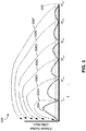
- FIG. 5 depicts a graph 500 of phase noise, which includes the quantization noise, over a frequency range in for a configuration of the PLL circuit 100 or 200 that includes an FIR filter with seven taps to operate with a transfer function that includes six notches.
- the plot 504 depicts quantization noise and other phase noise that is present in the digital filtered control signal in the output from the FIR filter.
- the lower amplitude broadband quantization noise spectrum 540 depicts noise that comes from the jitter of the output signal from the VCO 120. Since the output signal from the VCO 120 serves as the clock signal that controls the operations of the DAC array, the jitter in the output clock also affects the quantization noise of the DACs in the DAC array 118.
- the quantization noise as each of the frequencies f DIV to 6 f DIV in the plot 504 is near zero because the FIR filter includes notches centered at those frequencies.
- the FIR filters in the digital PLL circuits of 100 and 300 reduce or eliminate quantization noise at DC (0 Hz) caused by the "folding back" of high-frequency dither quantization noise to DC from aliasing in the feedback divider. Reducing the DC noise enables more efficient operation of the digital PLL circuit, which enables more power-efficient operation because the digital PLL circuit does not need to consume extra power to generate corrected output signals to overcome the effects of the DC quantization noise.
- the reductions in power consumption are beneficial to many electronic systems, and particularly to battery operated systems or other limited power source systems.
- the digital PLL circuits of FIG. 1 and FIG. 3 may be used in a wide variety of systems including, but not limited to, communication systems, sensor systems, clock and data recovery systems, microprocessors, and the like.
Landscapes
- Stabilization Of Oscillater, Synchronisation, Frequency Synthesizers (AREA)
Claims (4)
- Phasenregelschleifenschaltung, die Folgendes umfasst:a) einen Phasendetektor (108), der einen ersten Eingang, der konfiguriert ist, ein Referenzsignal mit einer vorgegebenen Wellenform mit einer vorgegebenen Frequenz zu empfangen, und einen zweiten Eingang, der konfiguriert ist, ein Rückkopplungssignal zu empfangen, aufweist, wobei der Phasendetektor (108) konfiguriert ist, auf der Grundlage des Referenzsignals und des Rückkopplungssignals ein digitales Steuersignal zu erzeugen;b) ein Schleifenfilter (112), das einen Eingang aufweist, der konfiguriert ist, das digitale Steuersignal von einem Ausgang des Phasendetektors (108) zu empfangen, wobei das Schleifenfilter (112) konfiguriert ist, ein gefiltertes, digitales Steuersignal zu erzeugen;c) einen Modulator (114), der einen Eingang aufweist, der konfiguriert ist, das gefilterte digitale Steuersignal von einem Ausgang des Schleifenfilters (112) zu empfangen, wobei der Modulator (114) konfiguriert ist, auf der Grundlage des gefilterten digitalen Steuersignals ein mit einer Schwingung überlagertes, digitales Steuersignal zu erzeugen;d) ein Filter (116) mit begrenzter Impulsantwort, FIR-Filter, das eine vorgegebene Anzahl von in Reihe geschalteten Abgriffen aufweist, wobei ein Ausgang des Modulators (114) mit einem ersten der vorgegebenen Anzahl von Abgriffen verbunden ist und das FIR-Filter (116) konfiguriert ist, ein Quantisierungsrauschen in dem mit einer Schwingung überlagerten digitalen Steuersignal zu verringern;e) mehrere DAC (214A-214K), wobei jeder DAC der mehreren DAC einen Eingang, der mit einem jeweiligen unterschiedlichen der vorgegebenen Anzahl von Abgriffen in dem FIR-Filter (116) verbunden ist, und einen Ausgang, der konfiguriert ist, ein jeweiliges analoges Steuersignal bereitzustellen, aufweist, wobei die Ausgänge der mehreren DAC (214A-214K) mit Eingängen einer Summierungsschaltung (215) verbunden sind, die konfiguriert ist, auf der Grundlage der Ausgänge der mehreren DAC (214A-214K) ein kombiniertes, analoges Steuersignal zu erzeugen;f) einen spannungsgesteuerten Oszillator, VCO, (120), der einen Eingang aufweist, der mit einem Ausgang der Summierungsschaltung (215) verbunden und konfiguriert ist, das kombinierte, analoge Steuersignal von der Summierungsschaltung (215) zu empfangen, wobei der VCO (120) konfiguriert ist, auf der Grundlage des kombinierten, analogen Steuersignals ein Ausgangssignal zu erzeugen, das eine Frequenz aufweist, die einem Vielfachen der vorgegebenen Frequenz des Referenzsignals entspricht; undg) einen ersten Frequenzteiler (122), der einen Eingang, der konfiguriert ist, das Ausgangssignal vom VCO (120) zu empfangen, und einen Ausgang, der konfiguriert ist, auf der Grundlage des Ausgangssignals das Rückkopplungssignal mit der vorgegebenen Frequenz des Referenzsignals für den zweiten Eingang des Phasendetektors (108) zu erzeugen, aufweist;h) einen zweiten Digital/Analog-Umsetzer-Frequenzteiler (124), der einen Eingang, der mit dem Ausgang des VCO (120) verbunden ist, und einen Ausgang, der mit jedem DAC der mehreren DAC (118) verbunden ist, aufweist;i) wobei der zweite Digital/Analog-Umsetzer-Frequenzteiler (124) konfiguriert ist, ein Taktsignal zu erzeugen, das eine Frequenz aufweist, die niedriger als die Frequenz des Ausgangssignal und mindestens das Zweifache der Frequenz des Referenzsignals ist, wobei jeder DAC der mehreren DAC konfiguriert ist, das Taktsignal zu empfangen, um sein jeweiliges digitales Eingangssignal mit einer Abtastfrequenz abzutasten, die die Taktsignalfrequenz ist;j) wobei die vorgegebene Anzahl von Abgriffen im FIR-Filter (116) einem Verhältnis der Abtastfrequenz zu der vorgegebenen Frequenz entspricht, wobei die Abtastfrequenz größer als die vorgegebene Frequenz ist.
- Phasenregelschleifenschaltung nach Anspruch 1, wobei die vorgegebene Anzahl von Abgriffen im FIR-Filter (116) für das Verhältnis der Abtastfrequenz der mehreren DAC (118) zur vorgegebenen Frequenz von zweiunddreißig zu eins zweiunddreißig ist.
- Phasenregelschleifenschaltung nach Anspruch 1, wobei die vorgegebene Anzahl von Abgriffen im FIR-Filter (116) für das Verhältnis der Abtastfrequenz der mehreren DAC (118) zur vorgegebenen Frequenz von acht zu eins acht ist.
- Phasenregelschleifenschaltung nach Anspruch 1, wobei die vorgegebene Anzahl von Abgriffen im FIR-Filter (116) konfiguriert ist, in einer Übertragungsfunktion des FIR-Filters (116) mehrere Kerben zu erzeugen, wobei die mehreren Kerben mindestens auf der vorgegebenen Frequenz (122) und auf das Zweifache der vorgegebenen Frequenz zentriert sind.
Applications Claiming Priority (2)
| Application Number | Priority Date | Filing Date | Title |
|---|---|---|---|
| US14/283,816 US9246499B2 (en) | 2014-05-21 | 2014-05-21 | Digital phase lock loop circuit including finite impulse response filtering to reduce aliasing of quantization noise |
| PCT/EP2015/061092 WO2015177200A1 (en) | 2014-05-21 | 2015-05-20 | Digital phase lock loop circuit including finite impulse response filtering to reduce aliasing of quantization noise |
Publications (2)
| Publication Number | Publication Date |
|---|---|
| EP3146632A1 EP3146632A1 (de) | 2017-03-29 |
| EP3146632B1 true EP3146632B1 (de) | 2021-07-07 |
Family
ID=53264647
Family Applications (1)
| Application Number | Title | Priority Date | Filing Date |
|---|---|---|---|
| EP15724255.3A Active EP3146632B1 (de) | 2014-05-21 | 2015-05-20 | Digitale phasenregelschleifenschaltung mit filterung mit endlicher impulsantwort zur reduzierung von aliasing von quantisierungsrauschen |
Country Status (3)
| Country | Link |
|---|---|
| US (1) | US9246499B2 (de) |
| EP (1) | EP3146632B1 (de) |
| WO (1) | WO2015177200A1 (de) |
Families Citing this family (12)
| Publication number | Priority date | Publication date | Assignee | Title |
|---|---|---|---|---|
| US9479325B1 (en) * | 2013-04-12 | 2016-10-25 | Maxim Integrated Products, Inc. | Reduced frequency backwards clock for isolated sigma-delta modulators |
| JP6439915B2 (ja) * | 2014-09-12 | 2018-12-19 | セイコーエプソン株式会社 | フラクショナルn−pll回路、発振器、電子機器及び移動体 |
| EP3096459A1 (de) * | 2015-05-20 | 2016-11-23 | Nxp B.V. | Phasenregelschleife mit verringertem rauschen |
| US9838026B2 (en) * | 2015-09-24 | 2017-12-05 | Analog Devices, Inc. | Apparatus and methods for fractional-N phase-locked loops with multi-phase oscillators |
| JP6818665B2 (ja) * | 2017-09-14 | 2021-01-20 | 株式会社東芝 | Da変換器及びadpll回路 |
| US10116314B1 (en) * | 2017-11-01 | 2018-10-30 | Nvidia Corporation | Multi-mode frequency divider |
| US10291389B1 (en) * | 2018-03-16 | 2019-05-14 | Stmicroelectronics International N.V. | Two-point modulator with matching gain calibration |
| US10868547B2 (en) * | 2018-09-25 | 2020-12-15 | Stmicroelectronics (Grenoble 2) Sas | Device for determining a propagation time |
| US10439631B1 (en) | 2018-12-27 | 2019-10-08 | Texas Instruments Incorporated | Radio-frequency digital-to-analog converter system |
| US11265009B2 (en) * | 2019-05-30 | 2022-03-01 | Texas Instruments Incorporated | Waveform synthesizer using multiple digital-to-analog converters |
| US10511312B1 (en) * | 2019-06-28 | 2019-12-17 | Silicon Laboratories Inc. | Metastable-free output synchronization for multiple-chip systems and the like |
| US11955979B2 (en) | 2022-06-08 | 2024-04-09 | Apple Inc. | Partial-fractional phase-locked loop with sigma delta modulator and finite impulse response filter |
Family Cites Families (19)
| Publication number | Priority date | Publication date | Assignee | Title |
|---|---|---|---|---|
| EP0600357A1 (de) * | 1992-11-30 | 1994-06-08 | Rim Tech, Inc. | Apparat und Verfahren zur Detektion und Messung der Dicke flüssigen Wassers und von Eis-Schichten auf festen Oberflächen |
| JP4552312B2 (ja) * | 2000-11-17 | 2010-09-29 | ソニー株式会社 | 信号処理回路 |
| US6990163B2 (en) * | 2000-11-21 | 2006-01-24 | Lsi Logic Corporation | Apparatus and method for acquiring phase lock timing recovery in a partial response maximum likelihood (PRML) channel |
| US7061276B2 (en) * | 2004-04-02 | 2006-06-13 | Teradyne, Inc. | Digital phase detector |
| US7492195B1 (en) * | 2005-06-22 | 2009-02-17 | Cypress Semiconductor Corp. | Agile, low phase noise clock synthesizer and jitter attenuator |
| US8411788B2 (en) * | 2005-11-18 | 2013-04-02 | Qualcomm, Incorporated | Digital transmitters for wireless communication |
| US7425874B2 (en) * | 2006-06-30 | 2008-09-16 | Texas Instruments Incorporated | All-digital phase-locked loop for a digital pulse-width modulator |
| US8204107B2 (en) * | 2008-04-09 | 2012-06-19 | National Semiconductor Corporation | Bandwidth reduction mechanism for polar modulation |
| US7760042B2 (en) * | 2008-06-26 | 2010-07-20 | Infineon Technologies Ag | Phase locked loop based frequency modulator with accurate oscillator gain adjustment |
| US8358729B2 (en) * | 2008-08-22 | 2013-01-22 | Finisar Corporation | Baseband phase-locked loop |
| GB2475664B (en) * | 2008-09-05 | 2012-11-07 | Icera Canada ULC | Method and system for calibrating a frequency synthesizer |
| GB2467379B (en) * | 2009-02-03 | 2013-05-22 | Cambridge Silicon Radio Ltd | Phase-locked loop |
| US8634512B2 (en) * | 2011-02-08 | 2014-01-21 | Qualcomm Incorporated | Two point modulation digital phase locked loop |
| KR20120125096A (ko) * | 2011-05-06 | 2012-11-14 | 삼성전자주식회사 | 디지털 제어 발진기를 포함하는 위상동기루프 회로 |
| US8508266B2 (en) * | 2011-06-30 | 2013-08-13 | Broadcom Corporation | Digital phase locked loop circuits with multiple digital feedback loops |
| US8618967B2 (en) * | 2012-03-30 | 2013-12-31 | Broadcom Corporation | Systems, circuits, and methods for a sigma-delta based time to digital converter |
| US8664989B1 (en) * | 2013-02-07 | 2014-03-04 | Cirrus Logic, Inc. | Method to increase frequency resolution of a fractional phase-locked loop |
| US8885788B1 (en) * | 2013-05-15 | 2014-11-11 | Intel IP Corporation | Reducing settling time in phase-locked loops |
| US9319051B2 (en) * | 2013-05-28 | 2016-04-19 | Broadcom Corporation | Digital PLL with hybrid phase/frequency detector and digital noise cancellation |
-
2014
- 2014-05-21 US US14/283,816 patent/US9246499B2/en active Active
-
2015
- 2015-05-20 EP EP15724255.3A patent/EP3146632B1/de active Active
- 2015-05-20 WO PCT/EP2015/061092 patent/WO2015177200A1/en not_active Ceased
Non-Patent Citations (1)
| Title |
|---|
| None * |
Also Published As
| Publication number | Publication date |
|---|---|
| EP3146632A1 (de) | 2017-03-29 |
| US20150341042A1 (en) | 2015-11-26 |
| WO2015177200A1 (en) | 2015-11-26 |
| US9246499B2 (en) | 2016-01-26 |
Similar Documents
| Publication | Publication Date | Title |
|---|---|---|
| EP3146632B1 (de) | Digitale phasenregelschleifenschaltung mit filterung mit endlicher impulsantwort zur reduzierung von aliasing von quantisierungsrauschen | |
| KR102427375B1 (ko) | 넓은 대역폭을 갖는 위상 동기 루프 회로 | |
| US10396808B2 (en) | Fractional-N phase lock loop apparatus and method using multi-element fractional dividers | |
| CN1768479B (zh) | 用于抖动补偿的方法和系统 | |
| US9319051B2 (en) | Digital PLL with hybrid phase/frequency detector and digital noise cancellation | |
| KR101786885B1 (ko) | 양자화 잡음을 제거하는 이진-가중 디지털 아날로그 미분기들을 구비한 델타-시그마 분수-n 주파수 신시사이저 | |
| US8994420B2 (en) | Higher-order phase noise modulator to reduce spurs and quantization noise | |
| EP2406884B1 (de) | Digitale phasenregelkreisarchitektur | |
| EP3888246B1 (de) | Synthese von fraktionaler frequenz durch sigma-delta-modulationsfrequenz eines referenztakts | |
| CN106209093A (zh) | 一种全数字小数分频锁相环结构 | |
| US7782104B2 (en) | Delay element array for time-to-digital converters | |
| CN116827336A (zh) | 一种基于电压空间均值的小数分频采样锁相环 | |
| US8995599B1 (en) | Techniques for generating fractional periodic signals | |
| EP4258552B1 (de) | Fraktional-n-adpll mit referenzdithering | |
| US8723607B2 (en) | Phase locked loop | |
| CN114244357B (zh) | 用于soc的全数字频率综合器及芯片 | |
| Tao et al. | ΔΣ fractional-N PLL with hybrid IIR noise filtering | |
| US10374618B1 (en) | Frequency locked loop with multi-bit sampler | |
| Wang | New strategies for low noise, agile PLL frequency synthesis | |
| Chi et al. | A fractional-N PLL for digital clock generation with an FIR-embedded frequency divider | |
| JP2015207805A (ja) | 位相同期回路および電子装置 | |
| Jung | Design of a low jitter digital PLL with low input frequency | |
| JP2012178808A (ja) | Pll回路 |
Legal Events
| Date | Code | Title | Description |
|---|---|---|---|
| STAA | Information on the status of an ep patent application or granted ep patent |
Free format text: STATUS: THE INTERNATIONAL PUBLICATION HAS BEEN MADE |
|
| PUAI | Public reference made under article 153(3) epc to a published international application that has entered the european phase |
Free format text: ORIGINAL CODE: 0009012 |
|
| STAA | Information on the status of an ep patent application or granted ep patent |
Free format text: STATUS: REQUEST FOR EXAMINATION WAS MADE |
|
| 17P | Request for examination filed |
Effective date: 20161221 |
|
| AK | Designated contracting states |
Kind code of ref document: A1 Designated state(s): AL AT BE BG CH CY CZ DE DK EE ES FI FR GB GR HR HU IE IS IT LI LT LU LV MC MK MT NL NO PL PT RO RS SE SI SK SM TR |
|
| AX | Request for extension of the european patent |
Extension state: BA ME |
|
| DAV | Request for validation of the european patent (deleted) | ||
| DAX | Request for extension of the european patent (deleted) | ||
| STAA | Information on the status of an ep patent application or granted ep patent |
Free format text: STATUS: EXAMINATION IS IN PROGRESS |
|
| 17Q | First examination report despatched |
Effective date: 20190403 |
|
| RAP1 | Party data changed (applicant data changed or rights of an application transferred) |
Owner name: ROBERT BOSCH GMBH |
|
| RIC1 | Information provided on ipc code assigned before grant |
Ipc: H03L 7/197 20060101ALI20201215BHEP Ipc: H03L 7/093 20060101AFI20201215BHEP |
|
| GRAP | Despatch of communication of intention to grant a patent |
Free format text: ORIGINAL CODE: EPIDOSNIGR1 |
|
| STAA | Information on the status of an ep patent application or granted ep patent |
Free format text: STATUS: GRANT OF PATENT IS INTENDED |
|
| INTG | Intention to grant announced |
Effective date: 20210129 |
|
| GRAS | Grant fee paid |
Free format text: ORIGINAL CODE: EPIDOSNIGR3 |
|
| GRAA | (expected) grant |
Free format text: ORIGINAL CODE: 0009210 |
|
| STAA | Information on the status of an ep patent application or granted ep patent |
Free format text: STATUS: THE PATENT HAS BEEN GRANTED |
|
| AK | Designated contracting states |
Kind code of ref document: B1 Designated state(s): AL AT BE BG CH CY CZ DE DK EE ES FI FR GB GR HR HU IE IS IT LI LT LU LV MC MK MT NL NO PL PT RO RS SE SI SK SM TR |
|
| REG | Reference to a national code |
Ref country code: GB Ref legal event code: FG4D |
|
| REG | Reference to a national code |
Ref country code: AT Ref legal event code: REF Ref document number: 1409568 Country of ref document: AT Kind code of ref document: T Effective date: 20210715 |
|
| REG | Reference to a national code |
Ref country code: DE Ref legal event code: R096 Ref document number: 602015071078 Country of ref document: DE |
|
| REG | Reference to a national code |
Ref country code: IE Ref legal event code: FG4D |
|
| REG | Reference to a national code |
Ref country code: LT Ref legal event code: MG9D |
|
| REG | Reference to a national code |
Ref country code: NL Ref legal event code: MP Effective date: 20210707 |
|
| REG | Reference to a national code |
Ref country code: AT Ref legal event code: MK05 Ref document number: 1409568 Country of ref document: AT Kind code of ref document: T Effective date: 20210707 |
|
| PG25 | Lapsed in a contracting state [announced via postgrant information from national office to epo] |
Ref country code: HR Free format text: LAPSE BECAUSE OF FAILURE TO SUBMIT A TRANSLATION OF THE DESCRIPTION OR TO PAY THE FEE WITHIN THE PRESCRIBED TIME-LIMIT Effective date: 20210707 Ref country code: RS Free format text: LAPSE BECAUSE OF FAILURE TO SUBMIT A TRANSLATION OF THE DESCRIPTION OR TO PAY THE FEE WITHIN THE PRESCRIBED TIME-LIMIT Effective date: 20210707 Ref country code: SE Free format text: LAPSE BECAUSE OF FAILURE TO SUBMIT A TRANSLATION OF THE DESCRIPTION OR TO PAY THE FEE WITHIN THE PRESCRIBED TIME-LIMIT Effective date: 20210707 Ref country code: FI Free format text: LAPSE BECAUSE OF FAILURE TO SUBMIT A TRANSLATION OF THE DESCRIPTION OR TO PAY THE FEE WITHIN THE PRESCRIBED TIME-LIMIT Effective date: 20210707 Ref country code: ES Free format text: LAPSE BECAUSE OF FAILURE TO SUBMIT A TRANSLATION OF THE DESCRIPTION OR TO PAY THE FEE WITHIN THE PRESCRIBED TIME-LIMIT Effective date: 20210707 Ref country code: NO Free format text: LAPSE BECAUSE OF FAILURE TO SUBMIT A TRANSLATION OF THE DESCRIPTION OR TO PAY THE FEE WITHIN THE PRESCRIBED TIME-LIMIT Effective date: 20211007 Ref country code: NL Free format text: LAPSE BECAUSE OF FAILURE TO SUBMIT A TRANSLATION OF THE DESCRIPTION OR TO PAY THE FEE WITHIN THE PRESCRIBED TIME-LIMIT Effective date: 20210707 Ref country code: PT Free format text: LAPSE BECAUSE OF FAILURE TO SUBMIT A TRANSLATION OF THE DESCRIPTION OR TO PAY THE FEE WITHIN THE PRESCRIBED TIME-LIMIT Effective date: 20211108 Ref country code: AT Free format text: LAPSE BECAUSE OF FAILURE TO SUBMIT A TRANSLATION OF THE DESCRIPTION OR TO PAY THE FEE WITHIN THE PRESCRIBED TIME-LIMIT Effective date: 20210707 Ref country code: BG Free format text: LAPSE BECAUSE OF FAILURE TO SUBMIT A TRANSLATION OF THE DESCRIPTION OR TO PAY THE FEE WITHIN THE PRESCRIBED TIME-LIMIT Effective date: 20211007 Ref country code: LT Free format text: LAPSE BECAUSE OF FAILURE TO SUBMIT A TRANSLATION OF THE DESCRIPTION OR TO PAY THE FEE WITHIN THE PRESCRIBED TIME-LIMIT Effective date: 20210707 |
|
| PG25 | Lapsed in a contracting state [announced via postgrant information from national office to epo] |
Ref country code: PL Free format text: LAPSE BECAUSE OF FAILURE TO SUBMIT A TRANSLATION OF THE DESCRIPTION OR TO PAY THE FEE WITHIN THE PRESCRIBED TIME-LIMIT Effective date: 20210707 Ref country code: LV Free format text: LAPSE BECAUSE OF FAILURE TO SUBMIT A TRANSLATION OF THE DESCRIPTION OR TO PAY THE FEE WITHIN THE PRESCRIBED TIME-LIMIT Effective date: 20210707 Ref country code: GR Free format text: LAPSE BECAUSE OF FAILURE TO SUBMIT A TRANSLATION OF THE DESCRIPTION OR TO PAY THE FEE WITHIN THE PRESCRIBED TIME-LIMIT Effective date: 20211008 |
|
| REG | Reference to a national code |
Ref country code: DE Ref legal event code: R097 Ref document number: 602015071078 Country of ref document: DE |
|
| PG25 | Lapsed in a contracting state [announced via postgrant information from national office to epo] |
Ref country code: DK Free format text: LAPSE BECAUSE OF FAILURE TO SUBMIT A TRANSLATION OF THE DESCRIPTION OR TO PAY THE FEE WITHIN THE PRESCRIBED TIME-LIMIT Effective date: 20210707 |
|
| PLBE | No opposition filed within time limit |
Free format text: ORIGINAL CODE: 0009261 |
|
| STAA | Information on the status of an ep patent application or granted ep patent |
Free format text: STATUS: NO OPPOSITION FILED WITHIN TIME LIMIT |
|
| PG25 | Lapsed in a contracting state [announced via postgrant information from national office to epo] |
Ref country code: SM Free format text: LAPSE BECAUSE OF FAILURE TO SUBMIT A TRANSLATION OF THE DESCRIPTION OR TO PAY THE FEE WITHIN THE PRESCRIBED TIME-LIMIT Effective date: 20210707 Ref country code: SK Free format text: LAPSE BECAUSE OF FAILURE TO SUBMIT A TRANSLATION OF THE DESCRIPTION OR TO PAY THE FEE WITHIN THE PRESCRIBED TIME-LIMIT Effective date: 20210707 Ref country code: RO Free format text: LAPSE BECAUSE OF FAILURE TO SUBMIT A TRANSLATION OF THE DESCRIPTION OR TO PAY THE FEE WITHIN THE PRESCRIBED TIME-LIMIT Effective date: 20210707 Ref country code: EE Free format text: LAPSE BECAUSE OF FAILURE TO SUBMIT A TRANSLATION OF THE DESCRIPTION OR TO PAY THE FEE WITHIN THE PRESCRIBED TIME-LIMIT Effective date: 20210707 Ref country code: CZ Free format text: LAPSE BECAUSE OF FAILURE TO SUBMIT A TRANSLATION OF THE DESCRIPTION OR TO PAY THE FEE WITHIN THE PRESCRIBED TIME-LIMIT Effective date: 20210707 Ref country code: AL Free format text: LAPSE BECAUSE OF FAILURE TO SUBMIT A TRANSLATION OF THE DESCRIPTION OR TO PAY THE FEE WITHIN THE PRESCRIBED TIME-LIMIT Effective date: 20210707 |
|
| 26N | No opposition filed |
Effective date: 20220408 |
|
| PG25 | Lapsed in a contracting state [announced via postgrant information from national office to epo] |
Ref country code: IT Free format text: LAPSE BECAUSE OF FAILURE TO SUBMIT A TRANSLATION OF THE DESCRIPTION OR TO PAY THE FEE WITHIN THE PRESCRIBED TIME-LIMIT Effective date: 20210707 |
|
| REG | Reference to a national code |
Ref country code: CH Ref legal event code: PL |
|
| REG | Reference to a national code |
Ref country code: BE Ref legal event code: MM Effective date: 20220531 |
|
| PG25 | Lapsed in a contracting state [announced via postgrant information from national office to epo] |
Ref country code: MC Free format text: LAPSE BECAUSE OF FAILURE TO SUBMIT A TRANSLATION OF THE DESCRIPTION OR TO PAY THE FEE WITHIN THE PRESCRIBED TIME-LIMIT Effective date: 20210707 Ref country code: LU Free format text: LAPSE BECAUSE OF NON-PAYMENT OF DUE FEES Effective date: 20220520 Ref country code: LI Free format text: LAPSE BECAUSE OF NON-PAYMENT OF DUE FEES Effective date: 20220531 Ref country code: CH Free format text: LAPSE BECAUSE OF NON-PAYMENT OF DUE FEES Effective date: 20220531 |
|
| PG25 | Lapsed in a contracting state [announced via postgrant information from national office to epo] |
Ref country code: IE Free format text: LAPSE BECAUSE OF NON-PAYMENT OF DUE FEES Effective date: 20220520 |
|
| PG25 | Lapsed in a contracting state [announced via postgrant information from national office to epo] |
Ref country code: BE Free format text: LAPSE BECAUSE OF NON-PAYMENT OF DUE FEES Effective date: 20220531 |
|
| PG25 | Lapsed in a contracting state [announced via postgrant information from national office to epo] |
Ref country code: HU Free format text: LAPSE BECAUSE OF FAILURE TO SUBMIT A TRANSLATION OF THE DESCRIPTION OR TO PAY THE FEE WITHIN THE PRESCRIBED TIME-LIMIT; INVALID AB INITIO Effective date: 20150520 |
|
| PG25 | Lapsed in a contracting state [announced via postgrant information from national office to epo] |
Ref country code: MK Free format text: LAPSE BECAUSE OF FAILURE TO SUBMIT A TRANSLATION OF THE DESCRIPTION OR TO PAY THE FEE WITHIN THE PRESCRIBED TIME-LIMIT Effective date: 20210707 Ref country code: CY Free format text: LAPSE BECAUSE OF FAILURE TO SUBMIT A TRANSLATION OF THE DESCRIPTION OR TO PAY THE FEE WITHIN THE PRESCRIBED TIME-LIMIT Effective date: 20210707 |
|
| PG25 | Lapsed in a contracting state [announced via postgrant information from national office to epo] |
Ref country code: TR Free format text: LAPSE BECAUSE OF FAILURE TO SUBMIT A TRANSLATION OF THE DESCRIPTION OR TO PAY THE FEE WITHIN THE PRESCRIBED TIME-LIMIT Effective date: 20210707 |
|
| PG25 | Lapsed in a contracting state [announced via postgrant information from national office to epo] |
Ref country code: MT Free format text: LAPSE BECAUSE OF FAILURE TO SUBMIT A TRANSLATION OF THE DESCRIPTION OR TO PAY THE FEE WITHIN THE PRESCRIBED TIME-LIMIT Effective date: 20210707 |
|
| PGFP | Annual fee paid to national office [announced via postgrant information from national office to epo] |
Ref country code: GB Payment date: 20250522 Year of fee payment: 11 |
|
| PGFP | Annual fee paid to national office [announced via postgrant information from national office to epo] |
Ref country code: FR Payment date: 20250523 Year of fee payment: 11 |
|
| PGFP | Annual fee paid to national office [announced via postgrant information from national office to epo] |
Ref country code: DE Payment date: 20250716 Year of fee payment: 11 |