EP3147909A1 - Verfahren zur kontrolle eines schreibzyklus eines speichers vom typ eeprom, und entsprechende vorrichtung - Google Patents
Verfahren zur kontrolle eines schreibzyklus eines speichers vom typ eeprom, und entsprechende vorrichtung Download PDFInfo
- Publication number
- EP3147909A1 EP3147909A1 EP16156143.6A EP16156143A EP3147909A1 EP 3147909 A1 EP3147909 A1 EP 3147909A1 EP 16156143 A EP16156143 A EP 16156143A EP 3147909 A1 EP3147909 A1 EP 3147909A1
- Authority
- EP
- European Patent Office
- Prior art keywords
- duration
- pulse
- value
- supply voltage
- write cycle
- Prior art date
- Legal status (The legal status is an assumption and is not a legal conclusion. Google has not performed a legal analysis and makes no representation as to the accuracy of the status listed.)
- Granted
Links
Images

Classifications
-
- G—PHYSICS
- G11—INFORMATION STORAGE
- G11C—STATIC STORES
- G11C16/00—Erasable programmable read-only memories
- G11C16/02—Erasable programmable read-only memories electrically programmable
- G11C16/06—Auxiliary circuits, e.g. for writing into memory
- G11C16/10—Programming or data input circuits
-
- G—PHYSICS
- G11—INFORMATION STORAGE
- G11C—STATIC STORES
- G11C13/00—Digital stores characterised by the use of storage elements not covered by groups G11C11/00, G11C23/00, or G11C25/00
- G11C13/0002—Digital stores characterised by the use of storage elements not covered by groups G11C11/00, G11C23/00, or G11C25/00 using resistive RAM [RRAM] elements
- G11C13/0021—Auxiliary circuits
- G11C13/0097—Erasing, e.g. resetting, circuits or methods
-
- G—PHYSICS
- G11—INFORMATION STORAGE
- G11C—STATIC STORES
- G11C13/00—Digital stores characterised by the use of storage elements not covered by groups G11C11/00, G11C23/00, or G11C25/00
- G11C13/0002—Digital stores characterised by the use of storage elements not covered by groups G11C11/00, G11C23/00, or G11C25/00 using resistive RAM [RRAM] elements
- G11C13/0021—Auxiliary circuits
- G11C13/0069—Writing or programming circuits or methods
-
- G—PHYSICS
- G11—INFORMATION STORAGE
- G11C—STATIC STORES
- G11C16/00—Erasable programmable read-only memories
- G11C16/02—Erasable programmable read-only memories electrically programmable
- G11C16/06—Auxiliary circuits, e.g. for writing into memory
- G11C16/10—Programming or data input circuits
- G11C16/14—Circuits for erasing electrically, e.g. erase voltage switching circuits
-
- G—PHYSICS
- G11—INFORMATION STORAGE
- G11C—STATIC STORES
- G11C16/00—Erasable programmable read-only memories
- G11C16/02—Erasable programmable read-only memories electrically programmable
- G11C16/06—Auxiliary circuits, e.g. for writing into memory
- G11C16/30—Power supply circuits
-
- G—PHYSICS
- G11—INFORMATION STORAGE
- G11C—STATIC STORES
- G11C16/00—Erasable programmable read-only memories
- G11C16/02—Erasable programmable read-only memories electrically programmable
- G11C16/06—Auxiliary circuits, e.g. for writing into memory
- G11C16/32—Timing circuits
-
- G—PHYSICS
- G11—INFORMATION STORAGE
- G11C—STATIC STORES
- G11C16/00—Erasable programmable read-only memories
- G11C16/02—Erasable programmable read-only memories electrically programmable
- G11C16/06—Auxiliary circuits, e.g. for writing into memory
- G11C16/34—Determination of programming status, e.g. threshold voltage, overprogramming or underprogramming, retention
- G11C16/3418—Disturbance prevention or evaluation; Refreshing of disturbed memory data
-
- G—PHYSICS
- G11—INFORMATION STORAGE
- G11C—STATIC STORES
- G11C29/00—Checking stores for correct operation ; Subsequent repair; Testing stores during standby or offline operation
- G11C29/02—Detection or location of defective auxiliary circuits, e.g. defective refresh counters
- G11C29/021—Detection or location of defective auxiliary circuits, e.g. defective refresh counters in voltage or current generators
-
- G—PHYSICS
- G11—INFORMATION STORAGE
- G11C—STATIC STORES
- G11C29/00—Checking stores for correct operation ; Subsequent repair; Testing stores during standby or offline operation
- G11C29/02—Detection or location of defective auxiliary circuits, e.g. defective refresh counters
- G11C29/028—Detection or location of defective auxiliary circuits, e.g. defective refresh counters with adaption or trimming of parameters
-
- G—PHYSICS
- G11—INFORMATION STORAGE
- G11C—STATIC STORES
- G11C29/00—Checking stores for correct operation ; Subsequent repair; Testing stores during standby or offline operation
- G11C29/04—Detection or location of defective memory elements, e.g. cell constructio details, timing of test signals
- G11C29/08—Functional testing, e.g. testing during refresh, power-on self testing [POST] or distributed testing
- G11C29/12—Built-in arrangements for testing, e.g. built-in self testing [BIST] or interconnection details
- G11C29/12005—Built-in arrangements for testing, e.g. built-in self testing [BIST] or interconnection details comprising voltage or current generators
-
- G—PHYSICS
- G11—INFORMATION STORAGE
- G11C—STATIC STORES
- G11C5/00—Details of stores covered by group G11C11/00
- G11C5/14—Power supply arrangements, e.g. power down, chip selection or deselection, layout of wirings or power grids, or multiple supply levels
- G11C5/143—Detection of memory cassette insertion or removal; Continuity checks of supply or ground lines; Detection of supply variations, interruptions or levels ; Switching between alternative supplies
- G11C5/144—Detection of predetermined disconnection or reduction of power supply, e.g. power down or power standby
Definitions
- Embodiments and embodiments of the invention relate to memories, in particular electrically erasable and programmable non-volatile memories (EEPROMs), and more particularly to the control of their write cycles.
- EEPROMs electrically erasable and programmable non-volatile memories
- An EEPROM memory cell generally comprises a transistor having a floating gate for storing the data, a control gate, a source region and a drain region. Such a memory cell uses the principle of nonvolatile storage of charges on the floating gate of the transistor.
- the operation or write cycle of a data comprises an erasure step followed by a programming step.
- the programming is done by Fowler-Nordheim effect using a voltage pulse having a high value, typically of the order of 13 to 15 volts, injecting electrons from the floating gate to the tunnel drain.
- Erasing is also done by the Fowler-Nordheim effect, electrons being injected by the tunnel tunneling effect from the drain to the floating gate, and is also carried out using an erase pulse similar to the programming pulse.
- the programming and erasing pulses are usually generated in the form of a ramp followed by a plateau, by pulse generating means conventionally comprising one or more charge pump stages.
- the current consumed during a write operation to be provided by the charge pump can be expressed as a DC component and a dynamic component (AC).
- the DC component of the current consumed comes mainly from the internal leakage currents of the transistors receiving the high voltage during the write operations, and if necessary the boxes in which these transistors are positioned.
- the dynamic component of the current consumed comes from the load of the different parasitic capacitances coming from the components and the interconnections receiving the high voltage during the writing operations.
- the current consumed is all the more important that the term dV / dt is large and therefore the expected write time is short.
- the same memory is capable of operating in a wide range of supply voltages, typically from 1.6 volts to 5.5 volts.
- generation means sized to be reliable with a short low voltage write time, for example 1.6V, are therefore oversized during high voltage operation, typically above 2.5 volts.
- an EEPROM memory capable of operating efficiently, in particular with regard to the charge pump, in a wide range of supply voltages, for example 1.6 volts - 5.5 volts.
- One proposed solution comprises a controlled adaptation of the write time as a function of the supply voltage, which enables the pulse generation means, in particular the charge pump, to operate efficiently as well as at low power. voltage at high voltage, without oversizing the charge pump which results in a saving of space.
- Controlled increase of the write cycle time ensures that the writing of the memory cells is correct, even in case of low supply voltage.
- the increase is controlled in that it is performed voluntarily and adjusted according to the amplitude of the drop in the supply voltage and therefore according to the current value of the supply voltage.
- the increase in the duration of the write cycle includes a increase by at least one step respectively corresponding to at least one step value of the supply voltage lower than a nominal value.
- Said at least one comparison can be made before the beginning of the write cycle, which makes it possible to perform the write cycle in an optimized configuration in terms of write time and reliability.
- the write operation generally comprises an erase step followed by a programming step
- a single erase or programming step it is possible, in certain cases, for a single erase or programming step to be necessary.
- to write a word in memory For example, if the word to be written contains only "0", then only one erase step is necessary, and likewise, when the word 0F (in hexadecimal notation) must be replaced by the word 1F, the step erasure is useless.
- the increase in the duration of the write cycle includes an increase in the duration of said at least one pulse.
- the increase in the duration of the write cycle may include an increase in the duration of each pulse.
- the pulse generating means generally includes one or more charge pump stages associated with charge pump control, and generates a high voltage pulse, usually in the form of a ramp followed by a plateau.
- the regulation controls the output voltage of the charge pump.
- the level of regulation can be for example the plateau voltage level, typically 15 volts.
- the duration of the pulse (ramp + plateau) is controlled by a timer ("timer”), analog or digital.
- the programming or erasure pulse generated by the charge pump stage (s) and the associated regulation, is applied to a circuit having a capacitive load as well as leakage currents.
- the output of the charge pump when the output of the charge pump is low, its current may for example be less than the current required for the capacitive load, in which case the pace of the ramp slows down and takes a curved shape. The plateau is then naturally shortened, the duration of the pulse being fixed by the stopwatch.
- the lower the power supply voltage the longer the pulse generation means provide the desired value of the plateau, the plateau may be too short and / or amplitude insufficient, and the writing may be incorrect.
- the time allocated to the ramp by the stopwatch is sufficiently long in case of low voltage, so that the generation of the ramp does not encroach on the time allocated to the plateau.
- increasing the duration of said at least one pulse may include increasing the duration of the corresponding ramp.
- the generation time of the plate is then sufficient for a reliable writing, and this makes it possible to maintain a fate of the correct charge pump by decreasing the importance of the term dV / dt of equation (1) mentioned above.
- the duration of the ramp and the total duration of the pulse are defined by two independent analog circuits that can lead to variations in decorrelated times.
- the proposed solution makes it possible to overcome the risks associated with the decorrelation of said variations.
- increasing the duration of said at least one pulse may include increasing the duration of the plateau.
- the writing operation is not impaired if the value of the plateau voltage decreases but its duration increases.
- increasing the duration of said at least one pulse may include decreasing the plateau voltage.
- the duration of said ramp is set to a nominal duration if the supply voltage is greater than said plateau value and is greater than said nominal duration if the supply voltage is lower than the plateau value.
- the nominal duration of the ramp may be substantially 0.25 ms and the duration greater than the nominal duration may be substantially 1 ms.
- the nominal durations of the ramps and trays are chosen so that, given their variations, the duration of a writing operation remains below a maximum guaranteed duration.
- the plateau value may be substantially 2.5V.
- a memory device intended to be powered by a supply voltage and comprising at least one memory cell electrically programmable and erasable read-only memory type, and control means of a write cycle configured to increase the duration of the write cycle in the presence of a decrease of said supply voltage.
- control means are configured to increase the duration of the write cycle by at least one step respectively corresponding to at least one step value of the supply voltage lower than a nominal value.
- control means comprise at least one means for comparing the current value of said supply voltage with said at least one step value.
- said at least one comparison means is configured to perform at least one comparison before the beginning of the write cycle.
- the device comprises writing means comprising means for generating at least one erase or programming pulse, and the control means are configured to increase the duration of the write cycle by increasing the duration of said at least one pulse.
- said generating means is configured to generate an erase pulse followed by a programming pulse
- the control means is configured to increase the duration of the write cycle by increasing the duration of each pulse .
- said generating means is configured to generate pulses comprising a voltage ramp followed by a plateau, and the control means are configured to increase the duration of said pulse by increasing the duration of the corresponding ramp.
- the control means may be configured to increase the duration of said pulse by increasing the duration of the corresponding plate.
- the control means may be configured to generate the plateau at a decreased value if the duration of said plateau is increased.
- control means are configured to generate the ramp for a fixed duration at a nominal duration if the supply voltage is greater than said plateau value and for a duration greater than said nominal duration if the voltage of supply is less than said plateau value.
- the value of the supply voltage may be between substantially 1.6V and substantially 5.5V and the plateau value may be substantially 2.5V.
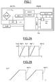
- the figure 1 schematically represents an EEPROM memory DIS device according to the invention.
- This device DIS is powered by power supply means ALIM comprising for example a battery or a battery, and comprises memory means MMEM and control means MCTRL.
- the memory means MMEM comprise a memory plane PM of memory cells CEL, as well as conventionally Decoder lines and columns DECX and DECY, and MECR writing means, conventional structures and known per se.
- the MECR writing means comprise in particular MGHV high voltage pulse generation means comprising in particular a ramp generator based for example on an analog integrator, a plurality of charge pump stages, an oscillator, and the associated regulation.
- the regulation controls the output voltage of the charge pump.
- the oscillator is stopped when the output of the charge pump exceeds a high reference.
- the output voltage of the charge pump then begins to decrease due to charging.
- the oscillator restarts.
- the voltage difference between the low and high references ensures stability. This voltage difference is for example of the order of 100 millivolts.
- the ramp is generated thanks in particular to the analog integrator comprising a capacitor, charged by a constant current, and followed by a voltage follower.
- the ramp can also be generated by regulating the charge pump itself. Indeed, the regulating voltage may itself be in the form of a ramp.
- the duration of the pulse is controlled by a timer ("timer”), analog or digital.
- a digital stopwatch may include a fixed frequency oscillator connected to a counter. The meter starts when the charge pump starts and the end of the count marks the end of the pulse.
- the characteristics of the plateau are determined in particular by the stopwatch and a set value.
- the MCTRL control means comprise MCMP comparison means and MCM control means comprising for example logic means of conventional structures in particular capable of controlling different elements of the control means MCTRL and MMEM storage, in particular elements of the MECR writing means.
- the comparison means MCMP comprise for example a comparator circuit, of conventional structure, in particular capable of comparing the value of the supply voltage with a control value, or plateau value, VPAL.
- the comparison means MCMP are also able to transmit the result of the comparison to the control means MCM, or to store it for example in a register SR.
- control means MCM in particular adjust the values of the currents and capacitances of the capacitors of the analog integrator and the charge pump regulation, the frequency of the oscillator, or the end of the counting of the counter, so that the pulse generating means generate the pulse in a longer or shorter duration.
- control means MCM will increase the values of the generator currents of the ramp, and / or decrease the capacitances of the capacitors charged by said currents.
- control means MCM will decrease the value of the generator currents of the ramp, and increase the capacitances of the capacitors charged by said currents.
- control means can increase the duration of the plateau, in particular by decreasing the frequency of the oscillator and increasing the end of the counter count.
- the MCM control means can also reduce the plateau voltage, for example by decreasing the high and low references of the charge pump regulator.
- the plateau is generated for a duration proportional to the generation duration of the corresponding ramp.
- Figures 2 to 5 represent pulse profiles generated by the same configuration of the MGHV pulse generation means, but controlled by the MCM control means for different supply voltages Vdd, and various embodiments or embodiments of the invention .
- the charge pump is especially sized to generate pulses with a short duration under supply voltage greater than the step value efficiently and with a consumption of the write operation compatible with the fan of the pump charge.
- This dimensioning also makes it possible to generate pulses of long duration at low supply voltage efficiently and according to a consumption of the write operation compatible with the output of the charge pump.
- the Figure 2A illustrates pulse profiles corresponding to an example of a short-duration write cycle with a supply voltage Vdd greater than the step value VPAL.
- the write operation is performed by an erase pulse IMP11 followed by a programming pulse IMP12.
- Each impulse IMP11, IMP12 has an RMP1 ramp followed by a PLT1 plateau typically at a nominal level Vplt of 15 volts.
- the duration of the write operation may be for example 1 ms, and each pulse IMP11, IMP12 may be of substantially the same duration, (t2-t0) of the order of 0.5 ms with durations (t1-t0) of the RMP1 ramp and (t2-t1) PLT1 plateau equal, of the order of 0.25 ms.
- pulses IMP11, IMP12 could have ramps and / or trays of different durations and / or different values.
- a decrease of the supply voltage Vdd below the value of the step VPAL causes an increase in the duration of the write cycle.
- the Figure 2B illustrates pulse patterns corresponding to a write cycle whose duration has been increased, in a situation where the supply voltage Vdd is lower than the stage value VPAL.
- the duration of the write operation may be for example 4 ms, and the erase pulse IMP21 and programming IMP22 may be of substantially the same duration.
- the pulses IMP21, IMP22 may have, according to the embodiments or implementation of the invention, ramps and / or trays of different durations and / or different values as will be detailed on the Figures 3 to 5 .
- the figure 3 illustrates a pulse IMP3 which may be either an erase or programming pulse, having an RMP3 ramp followed by a PLT3 plateau typically at a nominal level Vplt of 15 volts.
- This pulse IMP3 has a duration of the ramp RMP3 and a plateau duration PLT3 increased compared to the pulses represented in FIG. Figure 2A .
- the duration of the pulse IMP3 (t4-t0) may be equal to 2 ms, and the durations (t3-t0) of the ramp RMP3 and (t4-t3) of the PLT3 plateau are substantially equal, which may be about 1 ms.
- the figure 4 illustrates a pulse IMP4 which can be indifferently an erase or programming pulse, having a ramp RMP4 followed by a PLT4 plateau typically at a nominal level Vplt of 15 volts.
- This pulse IMP4 has an increased ramp time RMP4 and a plateau duration PLT4 not increased compared to the pulses represented in FIG. Figure 2A .
- the duration of the pulse IMP4 (t5-t0) may be about 1.25 ms, and the times (t3-t0) of the ramp RMP4 and (t5-t3) of the PLT4 plateau may be respectively about 1 ms and 0.25 ms.
- the figure 5 illustrates a pulse IMP5 which may be either an erase or programming pulse, having an RMP5 ramp followed by a PLT5 plateau at a level Vplt '.
- This pulse IMP5 has an increased ramp time RMP3 and plateau PLT5, and a plateau value decreased, compared to the pulses represented in FIG. Figure 2A .
- the PLT5 value Vplt ' is less than the value Vplt of the trays of the preceding embodiments, and can be for example 14V.
- the duration of the pulse IMP5 (t4-t0) may be about 2 ms, and the times (t3-t0) of the ramp RMP5 and (t4-t3) of the PLT5 plateau are substantially equal, being able to worth about 1 ms.
- the erasure and programming pulses may respectively not be identical in ramp time, amplitude, plateau duration, or total time.
Landscapes
- Read Only Memory (AREA)
Applications Claiming Priority (1)
| Application Number | Priority Date | Filing Date | Title |
|---|---|---|---|
| FR1559017A FR3041807B1 (fr) | 2015-09-24 | 2015-09-24 | Procede de controle d'un cycle d'ecriture de memoire de type eeprom et dispositif correspondant |
Publications (2)
| Publication Number | Publication Date |
|---|---|
| EP3147909A1 true EP3147909A1 (de) | 2017-03-29 |
| EP3147909B1 EP3147909B1 (de) | 2020-04-01 |
Family
ID=55361595
Family Applications (1)
| Application Number | Title | Priority Date | Filing Date |
|---|---|---|---|
| EP16156143.6A Active EP3147909B1 (de) | 2015-09-24 | 2016-02-17 | Verfahren zur kontrolle eines schreibzyklus eines speichers vom typ eeprom, und entsprechende vorrichtung |
Country Status (4)
| Country | Link |
|---|---|
| US (2) | US10068644B2 (de) |
| EP (1) | EP3147909B1 (de) |
| CN (2) | CN205406095U (de) |
| FR (1) | FR3041807B1 (de) |
Families Citing this family (4)
| Publication number | Priority date | Publication date | Assignee | Title |
|---|---|---|---|---|
| FR3041807B1 (fr) * | 2015-09-24 | 2017-12-08 | Stmicroelectronics Rousset | Procede de controle d'un cycle d'ecriture de memoire de type eeprom et dispositif correspondant |
| KR102277652B1 (ko) * | 2017-10-26 | 2021-07-14 | 삼성전자주식회사 | 워드 라인 불량 검출 회로를 포함하는 메모리 장치 및 그 구동 방법 |
| CN109343865B (zh) * | 2018-09-21 | 2021-09-28 | 四川长虹电器股份有限公司 | 一种提升烧写eeprom效率的方法 |
| US10741260B1 (en) * | 2019-05-28 | 2020-08-11 | Micron Technology, Inc. | Systems and methods providing improved calibration of memory control voltage |
Citations (6)
| Publication number | Priority date | Publication date | Assignee | Title |
|---|---|---|---|---|
| US5729494A (en) * | 1993-05-11 | 1998-03-17 | Nkk Corporation | Non-volatile memory with floating gate type cell transistors and method for adjusting threshold valves of these transistors |
| US6044015A (en) * | 1995-08-11 | 2000-03-28 | Imec Vzw | Method of programming a flash EEPROM memory cell array optimized for low power consumption |
| US20050207230A1 (en) * | 2003-07-31 | 2005-09-22 | Stmicroelectronics Sa | Method for erasing/programming a non-volatile electrically erasable memory |
| US20050207229A1 (en) * | 2004-03-22 | 2005-09-22 | Ken Takeuchi | Nonvolatile semiconductor memory |
| EP1783778A1 (de) * | 1998-06-30 | 2007-05-09 | SanDisk Corporation | Halbleiterspeicherschaltung mit interner Spannungserzeugung in Abhängigkeit von .der extern angelegten Versorgungsspannung |
| US20110194364A1 (en) * | 2010-02-09 | 2011-08-11 | Infineon Technologies Ag | Nvm overlapping write method |
Family Cites Families (16)
| Publication number | Priority date | Publication date | Assignee | Title |
|---|---|---|---|---|
| JPH08129894A (ja) * | 1994-10-28 | 1996-05-21 | Nec Corp | 不揮発性半導体記憶装置 |
| FR2749698B1 (fr) * | 1996-06-07 | 1998-09-04 | Inside Technologies | Memoire remanente effacable et programmable electriquement, protegee contre les coupures d'alimentation |
| FR2768846B1 (fr) * | 1997-09-19 | 1999-12-24 | Sgs Thomson Microelectronics | Procede et circuit de generation de la tension de programmation et d'effacement dans une memoire non volatile |
| FR2770326B1 (fr) * | 1997-10-28 | 2001-12-28 | Sgs Thomson Microelectronics | Procede d'ecriture dans une memoire non volatile modifiable electriquement |
| KR100277848B1 (ko) * | 1997-12-27 | 2001-01-15 | 김영환 | 반도체 메모리장치 |
| FR2821974B1 (fr) * | 2001-03-12 | 2003-05-23 | St Microelectronics Sa | Circuit et procede associe d'effacement ou de programmation d'une cellule memoire |
| US6735117B2 (en) * | 2002-07-01 | 2004-05-11 | Honeywell International Inc. | Hold-up power supply for flash memory |
| FR2890484A1 (fr) * | 2005-09-06 | 2007-03-09 | St Microelectronics Sa | Circuit integre sans contact passif comprenant un drapeau de surveillance d'une tension d'effacement-programmation. |
| US7330373B2 (en) * | 2006-03-28 | 2008-02-12 | Sandisk Corporation | Program time adjustment as function of program voltage for improved programming speed in memory system |
| US7457146B2 (en) * | 2006-06-19 | 2008-11-25 | Qimonda North America Corp. | Memory cell programmed using a temperature controlled set pulse |
| KR100967099B1 (ko) | 2008-09-10 | 2010-07-01 | 주식회사 하이닉스반도체 | 반도체 메모리 장치와 그의 구동 방법 |
| US8310300B2 (en) * | 2010-08-27 | 2012-11-13 | Freescale Semiconductor, Inc. | Charge pump having ramp rate control |
| DE102011056141A1 (de) * | 2010-12-20 | 2012-06-21 | Samsung Electronics Co., Ltd. | Negativspannungsgenerator, Dekoder, nicht-flüchtige Speichervorrichtung und Speichersystem, das eine negative Spannung verwendet |
| US9218851B2 (en) * | 2013-10-24 | 2015-12-22 | Sandisk Technologies Inc. | Power drop protection for a data storage device |
| FR3039921B1 (fr) * | 2015-08-06 | 2018-02-16 | Stmicroelectronics (Rousset) Sas | Procede et systeme de controle d'une operation d'ecriture d'une donnee dans une cellule-memoire du type eeprom |
| FR3041807B1 (fr) * | 2015-09-24 | 2017-12-08 | Stmicroelectronics Rousset | Procede de controle d'un cycle d'ecriture de memoire de type eeprom et dispositif correspondant |
-
2015
- 2015-09-24 FR FR1559017A patent/FR3041807B1/fr not_active Expired - Fee Related
-
2016
- 2016-02-17 EP EP16156143.6A patent/EP3147909B1/de active Active
- 2016-02-25 CN CN201620144215.5U patent/CN205406095U/zh not_active Expired - Lifetime
- 2016-02-25 US US15/054,015 patent/US10068644B2/en active Active
- 2016-02-25 CN CN201610105870.4A patent/CN106558340B/zh active Active
-
2018
- 2018-06-15 US US16/010,268 patent/US10210933B2/en active Active
Patent Citations (6)
| Publication number | Priority date | Publication date | Assignee | Title |
|---|---|---|---|---|
| US5729494A (en) * | 1993-05-11 | 1998-03-17 | Nkk Corporation | Non-volatile memory with floating gate type cell transistors and method for adjusting threshold valves of these transistors |
| US6044015A (en) * | 1995-08-11 | 2000-03-28 | Imec Vzw | Method of programming a flash EEPROM memory cell array optimized for low power consumption |
| EP1783778A1 (de) * | 1998-06-30 | 2007-05-09 | SanDisk Corporation | Halbleiterspeicherschaltung mit interner Spannungserzeugung in Abhängigkeit von .der extern angelegten Versorgungsspannung |
| US20050207230A1 (en) * | 2003-07-31 | 2005-09-22 | Stmicroelectronics Sa | Method for erasing/programming a non-volatile electrically erasable memory |
| US20050207229A1 (en) * | 2004-03-22 | 2005-09-22 | Ken Takeuchi | Nonvolatile semiconductor memory |
| US20110194364A1 (en) * | 2010-02-09 | 2011-08-11 | Infineon Technologies Ag | Nvm overlapping write method |
Also Published As
| Publication number | Publication date |
|---|---|
| CN205406095U (zh) | 2016-07-27 |
| US20170092357A1 (en) | 2017-03-30 |
| CN106558340B (zh) | 2021-02-26 |
| FR3041807B1 (fr) | 2017-12-08 |
| US10068644B2 (en) | 2018-09-04 |
| US10210933B2 (en) | 2019-02-19 |
| FR3041807A1 (fr) | 2017-03-31 |
| EP3147909B1 (de) | 2020-04-01 |
| CN106558340A (zh) | 2017-04-05 |
| US20180294030A1 (en) | 2018-10-11 |
Similar Documents
| Publication | Publication Date | Title |
|---|---|---|
| EP0394705B1 (de) | Festwertspeichersystem mit Mehrfachwert-Speicherung | |
| US7737765B2 (en) | Fast start charge pump for voltage regulators | |
| US8497667B2 (en) | Fast voltage regulators for charge pumps | |
| US5801987A (en) | Automatic transition charge pump for nonvolatile memories | |
| EP3147909B1 (de) | Verfahren zur kontrolle eines schreibzyklus eines speichers vom typ eeprom, und entsprechende vorrichtung | |
| EP0271686A2 (de) | Integriertes System zur Erzeugung von Spannungen verschiedener Höhen | |
| US8339187B2 (en) | Charge pump systems and methods | |
| CN108305659B (zh) | 非易失存储器擦写电压的斜率控制电路及非易失存储器 | |
| FR3056861A1 (fr) | Procede et systeme de gestion du fonctionnement d'oscillateurs en anneau | |
| US20120139622A1 (en) | Semiconductor apparatus voltage supply circuit | |
| EP0903750B1 (de) | Verfahren und Schaltung zur Erzeugung der Programmier- und Löschspannung in einem nichtflüchtigen Speicher | |
| JP5808937B2 (ja) | 半導体メモリの内部電源電圧生成回路及び内部電源電圧生成方法 | |
| EP0618657B1 (de) | Automatische Triggerschaltung | |
| EP1798626A1 (de) | Voltage regulation circuit, in particular for booster pump | |
| FR3048114A1 (fr) | Procede d'amelioration de l'operation d'ecriture dans une memoire eeprom et dispositif correspondant | |
| FR3039921A1 (fr) | Procede et systeme de controle d'une operation d'ecriture d'une donnee dans une cellule-memoire du type eeprom | |
| FR2847717A1 (fr) | Circuit limiteur de tension, notamment pour pompe de charge | |
| CN110299173B (zh) | 一种用于nor flash编程处理的可控放电模块 | |
| US5978268A (en) | Circuit for the generation of voltage for the programming or erasure of a memory that uses floating-gate transistors | |
| EP0811987B1 (de) | Hochprogrammierspannungsgeneratorschaltung | |
| US20020126534A1 (en) | Circuit and associated method for the erasure or programming of a memory cell | |
| FR2858457A1 (fr) | Procede d'effacement/programmation d'une memoire non volatile effacable electriquement | |
| KR100908537B1 (ko) | 고전압 제공 장치 | |
| JP2007066467A (ja) | 不揮発性半導体記憶装置 | |
| FR2809246A1 (fr) | Generateur de rampe a faible chute de tension serie |
Legal Events
| Date | Code | Title | Description |
|---|---|---|---|
| PUAI | Public reference made under article 153(3) epc to a published international application that has entered the european phase |
Free format text: ORIGINAL CODE: 0009012 |
|
| STAA | Information on the status of an ep patent application or granted ep patent |
Free format text: STATUS: REQUEST FOR EXAMINATION WAS MADE |
|
| 17P | Request for examination filed |
Effective date: 20160217 |
|
| AK | Designated contracting states |
Kind code of ref document: A1 Designated state(s): AL AT BE BG CH CY CZ DE DK EE ES FI FR GB GR HR HU IE IS IT LI LT LU LV MC MK MT NL NO PL PT RO RS SE SI SK SM TR |
|
| AX | Request for extension of the european patent |
Extension state: BA ME |
|
| STAA | Information on the status of an ep patent application or granted ep patent |
Free format text: STATUS: EXAMINATION IS IN PROGRESS |
|
| 17Q | First examination report despatched |
Effective date: 20180713 |
|
| GRAP | Despatch of communication of intention to grant a patent |
Free format text: ORIGINAL CODE: EPIDOSNIGR1 |
|
| STAA | Information on the status of an ep patent application or granted ep patent |
Free format text: STATUS: GRANT OF PATENT IS INTENDED |
|
| RIC1 | Information provided on ipc code assigned before grant |
Ipc: G11C 16/30 20060101AFI20190930BHEP Ipc: G11C 29/12 20060101ALN20190930BHEP Ipc: G11C 16/32 20060101ALI20190930BHEP Ipc: G11C 5/14 20060101ALN20190930BHEP Ipc: G11C 29/02 20060101ALN20190930BHEP Ipc: G11C 16/10 20060101ALI20190930BHEP Ipc: G11C 16/34 20060101ALN20190930BHEP Ipc: G11C 16/14 20060101ALI20190930BHEP |
|
| INTG | Intention to grant announced |
Effective date: 20191014 |
|
| GRAJ | Information related to disapproval of communication of intention to grant by the applicant or resumption of examination proceedings by the epo deleted |
Free format text: ORIGINAL CODE: EPIDOSDIGR1 |
|
| STAA | Information on the status of an ep patent application or granted ep patent |
Free format text: STATUS: EXAMINATION IS IN PROGRESS |
|
| REG | Reference to a national code |
Ref country code: DE Ref legal event code: R079 Ref document number: 602016032841 Country of ref document: DE Free format text: PREVIOUS MAIN CLASS: G11C0016100000 Ipc: G11C0016300000 |
|
| GRAR | Information related to intention to grant a patent recorded |
Free format text: ORIGINAL CODE: EPIDOSNIGR71 |
|
| GRAS | Grant fee paid |
Free format text: ORIGINAL CODE: EPIDOSNIGR3 |
|
| STAA | Information on the status of an ep patent application or granted ep patent |
Free format text: STATUS: GRANT OF PATENT IS INTENDED |
|
| INTC | Intention to grant announced (deleted) | ||
| GRAA | (expected) grant |
Free format text: ORIGINAL CODE: 0009210 |
|
| STAA | Information on the status of an ep patent application or granted ep patent |
Free format text: STATUS: THE PATENT HAS BEEN GRANTED |
|
| RIC1 | Information provided on ipc code assigned before grant |
Ipc: G11C 29/12 20060101ALN20200129BHEP Ipc: G11C 16/30 20060101AFI20200129BHEP Ipc: G11C 29/02 20060101ALN20200129BHEP Ipc: G11C 16/10 20060101ALI20200129BHEP Ipc: G11C 16/34 20060101ALN20200129BHEP Ipc: G11C 16/14 20060101ALI20200129BHEP Ipc: G11C 5/14 20060101ALN20200129BHEP Ipc: G11C 16/32 20060101ALI20200129BHEP |
|
| INTG | Intention to grant announced |
Effective date: 20200203 |
|
| AK | Designated contracting states |
Kind code of ref document: B1 Designated state(s): AL AT BE BG CH CY CZ DE DK EE ES FI FR GB GR HR HU IE IS IT LI LT LU LV MC MK MT NL NO PL PT RO RS SE SI SK SM TR |
|
| REG | Reference to a national code |
Ref country code: GB Ref legal event code: FG4D Free format text: NOT ENGLISH |
|
| REG | Reference to a national code |
Ref country code: AT Ref legal event code: REF Ref document number: 1252418 Country of ref document: AT Kind code of ref document: T Effective date: 20200415 Ref country code: CH Ref legal event code: EP |
|
| REG | Reference to a national code |
Ref country code: DE Ref legal event code: R096 Ref document number: 602016032841 Country of ref document: DE |
|
| REG | Reference to a national code |
Ref country code: IE Ref legal event code: FG4D Free format text: LANGUAGE OF EP DOCUMENT: FRENCH |
|
| PG25 | Lapsed in a contracting state [announced via postgrant information from national office to epo] |
Ref country code: BG Free format text: LAPSE BECAUSE OF FAILURE TO SUBMIT A TRANSLATION OF THE DESCRIPTION OR TO PAY THE FEE WITHIN THE PRESCRIBED TIME-LIMIT Effective date: 20200701 |
|
| REG | Reference to a national code |
Ref country code: NL Ref legal event code: MP Effective date: 20200401 |
|
| REG | Reference to a national code |
Ref country code: LT Ref legal event code: MG4D |
|
| PG25 | Lapsed in a contracting state [announced via postgrant information from national office to epo] |
Ref country code: FI Free format text: LAPSE BECAUSE OF FAILURE TO SUBMIT A TRANSLATION OF THE DESCRIPTION OR TO PAY THE FEE WITHIN THE PRESCRIBED TIME-LIMIT Effective date: 20200401 Ref country code: NO Free format text: LAPSE BECAUSE OF FAILURE TO SUBMIT A TRANSLATION OF THE DESCRIPTION OR TO PAY THE FEE WITHIN THE PRESCRIBED TIME-LIMIT Effective date: 20200701 Ref country code: SE Free format text: LAPSE BECAUSE OF FAILURE TO SUBMIT A TRANSLATION OF THE DESCRIPTION OR TO PAY THE FEE WITHIN THE PRESCRIBED TIME-LIMIT Effective date: 20200401 Ref country code: PT Free format text: LAPSE BECAUSE OF FAILURE TO SUBMIT A TRANSLATION OF THE DESCRIPTION OR TO PAY THE FEE WITHIN THE PRESCRIBED TIME-LIMIT Effective date: 20200817 Ref country code: CZ Free format text: LAPSE BECAUSE OF FAILURE TO SUBMIT A TRANSLATION OF THE DESCRIPTION OR TO PAY THE FEE WITHIN THE PRESCRIBED TIME-LIMIT Effective date: 20200401 Ref country code: NL Free format text: LAPSE BECAUSE OF FAILURE TO SUBMIT A TRANSLATION OF THE DESCRIPTION OR TO PAY THE FEE WITHIN THE PRESCRIBED TIME-LIMIT Effective date: 20200401 Ref country code: LT Free format text: LAPSE BECAUSE OF FAILURE TO SUBMIT A TRANSLATION OF THE DESCRIPTION OR TO PAY THE FEE WITHIN THE PRESCRIBED TIME-LIMIT Effective date: 20200401 Ref country code: GR Free format text: LAPSE BECAUSE OF FAILURE TO SUBMIT A TRANSLATION OF THE DESCRIPTION OR TO PAY THE FEE WITHIN THE PRESCRIBED TIME-LIMIT Effective date: 20200702 Ref country code: IS Free format text: LAPSE BECAUSE OF FAILURE TO SUBMIT A TRANSLATION OF THE DESCRIPTION OR TO PAY THE FEE WITHIN THE PRESCRIBED TIME-LIMIT Effective date: 20200801 |
|
| REG | Reference to a national code |
Ref country code: AT Ref legal event code: MK05 Ref document number: 1252418 Country of ref document: AT Kind code of ref document: T Effective date: 20200401 |
|
| PG25 | Lapsed in a contracting state [announced via postgrant information from national office to epo] |
Ref country code: RS Free format text: LAPSE BECAUSE OF FAILURE TO SUBMIT A TRANSLATION OF THE DESCRIPTION OR TO PAY THE FEE WITHIN THE PRESCRIBED TIME-LIMIT Effective date: 20200401 Ref country code: HR Free format text: LAPSE BECAUSE OF FAILURE TO SUBMIT A TRANSLATION OF THE DESCRIPTION OR TO PAY THE FEE WITHIN THE PRESCRIBED TIME-LIMIT Effective date: 20200401 Ref country code: LV Free format text: LAPSE BECAUSE OF FAILURE TO SUBMIT A TRANSLATION OF THE DESCRIPTION OR TO PAY THE FEE WITHIN THE PRESCRIBED TIME-LIMIT Effective date: 20200401 |
|
| PG25 | Lapsed in a contracting state [announced via postgrant information from national office to epo] |
Ref country code: AL Free format text: LAPSE BECAUSE OF FAILURE TO SUBMIT A TRANSLATION OF THE DESCRIPTION OR TO PAY THE FEE WITHIN THE PRESCRIBED TIME-LIMIT Effective date: 20200401 |
|
| REG | Reference to a national code |
Ref country code: DE Ref legal event code: R097 Ref document number: 602016032841 Country of ref document: DE |
|
| PG25 | Lapsed in a contracting state [announced via postgrant information from national office to epo] |
Ref country code: SM Free format text: LAPSE BECAUSE OF FAILURE TO SUBMIT A TRANSLATION OF THE DESCRIPTION OR TO PAY THE FEE WITHIN THE PRESCRIBED TIME-LIMIT Effective date: 20200401 Ref country code: RO Free format text: LAPSE BECAUSE OF FAILURE TO SUBMIT A TRANSLATION OF THE DESCRIPTION OR TO PAY THE FEE WITHIN THE PRESCRIBED TIME-LIMIT Effective date: 20200401 Ref country code: IT Free format text: LAPSE BECAUSE OF FAILURE TO SUBMIT A TRANSLATION OF THE DESCRIPTION OR TO PAY THE FEE WITHIN THE PRESCRIBED TIME-LIMIT Effective date: 20200401 Ref country code: ES Free format text: LAPSE BECAUSE OF FAILURE TO SUBMIT A TRANSLATION OF THE DESCRIPTION OR TO PAY THE FEE WITHIN THE PRESCRIBED TIME-LIMIT Effective date: 20200401 Ref country code: EE Free format text: LAPSE BECAUSE OF FAILURE TO SUBMIT A TRANSLATION OF THE DESCRIPTION OR TO PAY THE FEE WITHIN THE PRESCRIBED TIME-LIMIT Effective date: 20200401 Ref country code: DK Free format text: LAPSE BECAUSE OF FAILURE TO SUBMIT A TRANSLATION OF THE DESCRIPTION OR TO PAY THE FEE WITHIN THE PRESCRIBED TIME-LIMIT Effective date: 20200401 Ref country code: AT Free format text: LAPSE BECAUSE OF FAILURE TO SUBMIT A TRANSLATION OF THE DESCRIPTION OR TO PAY THE FEE WITHIN THE PRESCRIBED TIME-LIMIT Effective date: 20200401 |
|
| PLBE | No opposition filed within time limit |
Free format text: ORIGINAL CODE: 0009261 |
|
| STAA | Information on the status of an ep patent application or granted ep patent |
Free format text: STATUS: NO OPPOSITION FILED WITHIN TIME LIMIT |
|
| PG25 | Lapsed in a contracting state [announced via postgrant information from national office to epo] |
Ref country code: PL Free format text: LAPSE BECAUSE OF FAILURE TO SUBMIT A TRANSLATION OF THE DESCRIPTION OR TO PAY THE FEE WITHIN THE PRESCRIBED TIME-LIMIT Effective date: 20200401 Ref country code: SK Free format text: LAPSE BECAUSE OF FAILURE TO SUBMIT A TRANSLATION OF THE DESCRIPTION OR TO PAY THE FEE WITHIN THE PRESCRIBED TIME-LIMIT Effective date: 20200401 |
|
| 26N | No opposition filed |
Effective date: 20210112 |
|
| PG25 | Lapsed in a contracting state [announced via postgrant information from national office to epo] |
Ref country code: SI Free format text: LAPSE BECAUSE OF FAILURE TO SUBMIT A TRANSLATION OF THE DESCRIPTION OR TO PAY THE FEE WITHIN THE PRESCRIBED TIME-LIMIT Effective date: 20200401 |
|
| PG25 | Lapsed in a contracting state [announced via postgrant information from national office to epo] |
Ref country code: MC Free format text: LAPSE BECAUSE OF FAILURE TO SUBMIT A TRANSLATION OF THE DESCRIPTION OR TO PAY THE FEE WITHIN THE PRESCRIBED TIME-LIMIT Effective date: 20200401 |
|
| GBPC | Gb: european patent ceased through non-payment of renewal fee |
Effective date: 20210217 |
|
| REG | Reference to a national code |
Ref country code: BE Ref legal event code: MM Effective date: 20210228 |
|
| PG25 | Lapsed in a contracting state [announced via postgrant information from national office to epo] |
Ref country code: LI Free format text: LAPSE BECAUSE OF NON-PAYMENT OF DUE FEES Effective date: 20210228 Ref country code: LU Free format text: LAPSE BECAUSE OF NON-PAYMENT OF DUE FEES Effective date: 20210217 Ref country code: CH Free format text: LAPSE BECAUSE OF NON-PAYMENT OF DUE FEES Effective date: 20210228 |
|
| PG25 | Lapsed in a contracting state [announced via postgrant information from national office to epo] |
Ref country code: FR Free format text: LAPSE BECAUSE OF NON-PAYMENT OF DUE FEES Effective date: 20210228 Ref country code: IE Free format text: LAPSE BECAUSE OF NON-PAYMENT OF DUE FEES Effective date: 20210217 Ref country code: GB Free format text: LAPSE BECAUSE OF NON-PAYMENT OF DUE FEES Effective date: 20210217 |
|
| PG25 | Lapsed in a contracting state [announced via postgrant information from national office to epo] |
Ref country code: BE Free format text: LAPSE BECAUSE OF NON-PAYMENT OF DUE FEES Effective date: 20210228 |
|
| PG25 | Lapsed in a contracting state [announced via postgrant information from national office to epo] |
Ref country code: HU Free format text: LAPSE BECAUSE OF FAILURE TO SUBMIT A TRANSLATION OF THE DESCRIPTION OR TO PAY THE FEE WITHIN THE PRESCRIBED TIME-LIMIT; INVALID AB INITIO Effective date: 20160217 |
|
| PG25 | Lapsed in a contracting state [announced via postgrant information from national office to epo] |
Ref country code: CY Free format text: LAPSE BECAUSE OF FAILURE TO SUBMIT A TRANSLATION OF THE DESCRIPTION OR TO PAY THE FEE WITHIN THE PRESCRIBED TIME-LIMIT Effective date: 20200401 |
|
| PG25 | Lapsed in a contracting state [announced via postgrant information from national office to epo] |
Ref country code: MK Free format text: LAPSE BECAUSE OF FAILURE TO SUBMIT A TRANSLATION OF THE DESCRIPTION OR TO PAY THE FEE WITHIN THE PRESCRIBED TIME-LIMIT Effective date: 20200401 |
|
| PG25 | Lapsed in a contracting state [announced via postgrant information from national office to epo] |
Ref country code: MT Free format text: LAPSE BECAUSE OF FAILURE TO SUBMIT A TRANSLATION OF THE DESCRIPTION OR TO PAY THE FEE WITHIN THE PRESCRIBED TIME-LIMIT Effective date: 20200401 |
|
| PGFP | Annual fee paid to national office [announced via postgrant information from national office to epo] |
Ref country code: DE Payment date: 20250122 Year of fee payment: 10 |
|
| PG25 | Lapsed in a contracting state [announced via postgrant information from national office to epo] |
Ref country code: TR Free format text: LAPSE BECAUSE OF FAILURE TO SUBMIT A TRANSLATION OF THE DESCRIPTION OR TO PAY THE FEE WITHIN THE PRESCRIBED TIME-LIMIT Effective date: 20200401 |