EP3147916A1 - Verfahren zur herstellung eines planaren pcb transformators - Google Patents
Verfahren zur herstellung eines planaren pcb transformators Download PDFInfo
- Publication number
- EP3147916A1 EP3147916A1 EP16195955.6A EP16195955A EP3147916A1 EP 3147916 A1 EP3147916 A1 EP 3147916A1 EP 16195955 A EP16195955 A EP 16195955A EP 3147916 A1 EP3147916 A1 EP 3147916A1
- Authority
- EP
- European Patent Office
- Prior art keywords
- layers
- windings
- conductive layers
- group
- isolation material
- Prior art date
- Legal status (The legal status is an assumption and is not a legal conclusion. Google has not performed a legal analysis and makes no representation as to the accuracy of the status listed.)
- Withdrawn
Links
- 238000000034 method Methods 0.000 title claims abstract description 23
- 238000002955 isolation Methods 0.000 claims abstract description 116
- 238000004804 winding Methods 0.000 claims abstract description 116
- 239000000463 material Substances 0.000 claims abstract description 98
- 238000004519 manufacturing process Methods 0.000 claims abstract description 23
- 239000000758 substrate Substances 0.000 claims description 42
- 230000008569 process Effects 0.000 claims description 10
- 239000010410 layer Substances 0.000 description 355
- 239000002184 metal Substances 0.000 description 44
- 229910052751 metal Inorganic materials 0.000 description 44
- 230000008878 coupling Effects 0.000 description 14
- 238000010168 coupling process Methods 0.000 description 14
- 238000005859 coupling reaction Methods 0.000 description 14
- 230000003071 parasitic effect Effects 0.000 description 11
- CJDNEKOMKXLSBN-UHFFFAOYSA-N 1-chloro-3-(4-chlorophenyl)benzene Chemical compound C1=CC(Cl)=CC=C1C1=CC=CC(Cl)=C1 CJDNEKOMKXLSBN-UHFFFAOYSA-N 0.000 description 6
- RYGMFSIKBFXOCR-UHFFFAOYSA-N Copper Chemical compound [Cu] RYGMFSIKBFXOCR-UHFFFAOYSA-N 0.000 description 6
- 229910052802 copper Inorganic materials 0.000 description 6
- 239000010949 copper Substances 0.000 description 6
- 150000003071 polychlorinated biphenyls Chemical class 0.000 description 4
- 238000010586 diagram Methods 0.000 description 2
- 239000002356 single layer Substances 0.000 description 2
- 239000000654 additive Substances 0.000 description 1
- 230000000996 additive effect Effects 0.000 description 1
- FFBHFFJDDLITSX-UHFFFAOYSA-N benzyl N-[2-hydroxy-4-(3-oxomorpholin-4-yl)phenyl]carbamate Chemical compound OC1=C(NC(=O)OCC2=CC=CC=C2)C=CC(=C1)N1CCOCC1=O FFBHFFJDDLITSX-UHFFFAOYSA-N 0.000 description 1
- 238000010276 construction Methods 0.000 description 1
- 230000003247 decreasing effect Effects 0.000 description 1
- 239000012530 fluid Substances 0.000 description 1
- 230000004907 flux Effects 0.000 description 1
- 230000006872 improvement Effects 0.000 description 1
- 239000000696 magnetic material Substances 0.000 description 1
- 238000012986 modification Methods 0.000 description 1
- 230000004048 modification Effects 0.000 description 1
- 238000007747 plating Methods 0.000 description 1
- 238000003825 pressing Methods 0.000 description 1
- 239000007787 solid Substances 0.000 description 1
- 230000001131 transforming effect Effects 0.000 description 1
- 238000007514 turning Methods 0.000 description 1
Images


Classifications
-
- H—ELECTRICITY
- H01—ELECTRIC ELEMENTS
- H01F—MAGNETS; INDUCTANCES; TRANSFORMERS; SELECTION OF MATERIALS FOR THEIR MAGNETIC PROPERTIES
- H01F27/00—Details of transformers or inductances, in general
- H01F27/28—Coils; Windings; Conductive connections
- H01F27/2804—Printed windings
-
- H—ELECTRICITY
- H01—ELECTRIC ELEMENTS
- H01F—MAGNETS; INDUCTANCES; TRANSFORMERS; SELECTION OF MATERIALS FOR THEIR MAGNETIC PROPERTIES
- H01F27/00—Details of transformers or inductances, in general
- H01F27/28—Coils; Windings; Conductive connections
- H01F27/32—Insulating of coils, windings, or parts thereof
- H01F27/323—Insulation between winding turns, between winding layers
-
- H—ELECTRICITY
- H01—ELECTRIC ELEMENTS
- H01F—MAGNETS; INDUCTANCES; TRANSFORMERS; SELECTION OF MATERIALS FOR THEIR MAGNETIC PROPERTIES
- H01F41/00—Apparatus or processes specially adapted for manufacturing or assembling magnets, inductances or transformers; Apparatus or processes specially adapted for manufacturing materials characterised by their magnetic properties
- H01F41/02—Apparatus or processes specially adapted for manufacturing or assembling magnets, inductances or transformers; Apparatus or processes specially adapted for manufacturing materials characterised by their magnetic properties for manufacturing cores, coils, or magnets
- H01F41/04—Apparatus or processes specially adapted for manufacturing or assembling magnets, inductances or transformers; Apparatus or processes specially adapted for manufacturing materials characterised by their magnetic properties for manufacturing cores, coils, or magnets for manufacturing coils
- H01F41/041—Printed circuit coils
-
- Y—GENERAL TAGGING OF NEW TECHNOLOGICAL DEVELOPMENTS; GENERAL TAGGING OF CROSS-SECTIONAL TECHNOLOGIES SPANNING OVER SEVERAL SECTIONS OF THE IPC; TECHNICAL SUBJECTS COVERED BY FORMER USPC CROSS-REFERENCE ART COLLECTIONS [XRACs] AND DIGESTS
- Y10—TECHNICAL SUBJECTS COVERED BY FORMER USPC
- Y10T—TECHNICAL SUBJECTS COVERED BY FORMER US CLASSIFICATION
- Y10T29/00—Metal working
- Y10T29/49—Method of mechanical manufacture
- Y10T29/49002—Electrical device making
- Y10T29/4902—Electromagnet, transformer or inductor
Definitions
- Embodiments disclosed herein relate to the field of planar magnetic transformers and, in particular, the arrangement of the windings used for a planar magnetic transformer on a multi-layered printed circuit board.
- Transformers are magnetic components that have many uses, such as for transforming voltages and for providing isolation between the circuits on the primary and secondary sides of the transformer.
- planar magnetic components have become widely used in power electronic devices, such as switched mode power supplies (SMPSs).
- SMPSs switched mode power supplies
- Figure 1 An example of an SMPS constructed with planar magnetic components is shown in Figure 1 .
- a planar magnetic component comprises two pieces of magnetic material (usually referred to as “cores”, but sometimes referred to as “half-cores”) which are used with one or more flat coils (also referred to as turns) printed on a printed circuit board (PCB).
- cores usually referred to as "cores”, but sometimes referred to as “half-cores”
- PCB printed circuit board
- one core is positioned above the one or more coils and a second, identical, core is positioned below the one or more coils, with the cores being connected together through at least one hole in the PCB.
- FIG. 2 by way of example, the parts of a planar magnetic transformer are shown unassembled.
- An upper core 11 and a lower core 12 are provided respectively above and below a multi-layered PCB 13.
- Cores 11 and 12 are identical E-plane cores.
- the layers of the PCB comprise at least one hole to allow the central part of each core to extend into the PCB 13.
- the PCB 13 would also contain holes, not shown in Figure 2 , to allow the outer wings of the "E" of each core to also extend into the PCB 13.
- Printed tracks on the layers of the PCB 13 provide coils round the centre part of the core as well as input and output connections to the transformer. The coils on each layer either provide a winding for the primary side of the transformer or a winding for the secondary side.
- the upper core 11 and the lower core 12 are attached to each other by the mechanical clip 14.
- the mechanical clip 14 extends around the edges of the PCB 13 and the ends of the mechanical clip 14 are attached to the recesses 15, 16 in the top surface of the upper core 11.
- a single mechanical clip is shown, two mechanical clips may alternatively have been used with separate clips attaching to respective ends of the upper and lower cores.
- the two cores may alternatively have been glued together instead of mechanical clips being used.
- primary and secondary windings are provided by using a multi-layered PCB such as the arrangement shown in Figure 2 .
- a multi-layered PCB such as the arrangement shown in Figure 2 .
- a plurality of coils, or turns are provided on each layer of the PCB.
- only a single coil, or turn may be used on each layer.
- the transformer shown in Figure 2 has the layers comprising printed tracks, that provide the coils of the transformer, fully interleaved. That is to say, for layers within the structure (i.e. those between the top and bottom layers), each layer that provides a coil of the primary windings of the transformer is directly adjacent, i.e. above and below, two layers that provide coils of the secondary side of a transformer. Similarly, each layer that provides a coil of the secondary side of the transformer is directly adjacent to layers that provide coils of the primary side of the transformer. In this way, no layer providing a primary winding is adjacent another layer providing a primary winding. Similarly, no layer providing a secondary winding is adjacent another layer providing a secondary winding.
- Figure 3 is a vertical cross-section of a multi-layered PCB showing the windings of a fully interleaved transformer with twelve layers.
- the outer layers i.e. the top and bottom layers in Fig. 3
- the inner layers each have a metal thickness t i , with t i greater than t o .
- the metal used to form the layers is typically copper.
- the isolation material is typically a plastic substrate.
- the thickness of the isolation material between the layers is h h .
- Figure 3 shows a known arrangement in which the spacing h h between each of the layers is the same throughout the vertical cross-section of the PCB.
- a problem experienced by the fully interleaved PCB shown in Fig. 3 is that the parasitic capacitive coupling between the primary and secondary windings is large.
- a way of reducing the parasitic capacitive coupling is to increase the thickness of the isolation material between the layers so that the metal layers within the PCB are spaced further apart from each other.
- increasing the spacing between the layers results in the parasitic leakage inductance increasing.
- a standard isolation voltage is 2250V between the primary and secondary sides. This imposes strict requirements on the isolation material and the distances between the primary and secondary windings.
- a solid plastic substrate also referred to as a laminate, is typically used as the isolation material.
- Tracks of the PCB are formed on the upper and lower surfaces from the substrate either by a subtractive process from a substrate with upper and lower surfaces entirely covered by metal or by an additive process onto a substrate without metal coverings on its upper and lower surfaces.
- the upper and lower layers of the PCB are then added using a pre-preg process again and forming the thinner upper and lower metal layers thereon.
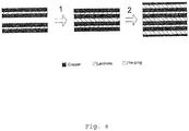
- Figure 4 shows a vertical cross-section of an entire PCB at stages during the manufacture of a PCB with six metal layers.
- process 1 shows the bonding between multiple substrates, with metal tracks on their upper and lower surfaces, with pre-preg.
- Process 2 shows the subsequent adding of the upper and lower metal surfaces of the PCB.
- the thickness of a layer is the dimension of a layer in a direction that is normal to the upper or lower surface of one of the planar layers.
- the layers of pre-preg are thicker than those of the substrate.
- Layers formed by a pre-preg process cannot be formed as thin as layers of substrate due to the nature of the pre-preg process.
- Standard manufacturing processes have a ⁇ 10% tolerance on the thickness of the layers.
- the minimum substrate thickness that can be designed for is about 100 ⁇ m and the minimum pre-preg thickness that can be designed for is about 150 ⁇ m.
- the minimum actual substrate and pre-preg thicknesses may be as low as 90 ⁇ m and 135 ⁇ m, respectively, due to the ⁇ 10% manufacturing tolerance.
- the average thickness of the pre-preg layer is required to be thicker than that of the substrate layer in order for it to be possible for the pre-preg to fill in the gaps between the printed tracks in the metal layers.
- the pre-preg isolation material In order to provide an isolation voltage of 2250V between the primary and secondary sides of the transformer, the pre-preg isolation material should be designed to have a minimum thickness of 175 ⁇ m. That is to say, due to the manufacturing tolerance, the pre-preg isolation material meets the 2250V requirement if it has a thickness of at least 157.5 ⁇ m.
- the isolation material in the fully interleaved transformer shown in Figure 3 must be designed to be at least 175 ⁇ m thick, h h ⁇ 175 ⁇ m, and the minimum manufacturable thicknesses of substrate and pre-preg cannot be used.
- the height of a PCB is the dimension of the PCB in a direction normal to the upper or lower surface of one of the planar layers.
- Embodiments provide multi-layered PCBs for planar magnetic transformers that overcome some or all of the above-identified problems.
- An embodiment provides a multi-layered printed circuit board, PCB, for providing first turns for a first side of a planar magnetic transformer and second turns for a second side of the planar magnetic transformer, the multi-layered PCB comprising: a plurality of conductive layers configured to provide the first turns; a plurality of conductive layers configured to provide the second turns; and a plurality of layers of an isolation material; wherein: each layer of isolation material is arranged between two conductive layers so as to provide electrical isolation between said two conductive layers; and a group of two or more adjacent conductive layers are all conductive layers of the first turns and are all arranged between conductive layers of the second turns, wherein the thickness of the isolation material between at least a pair of adjacent conductive layers in the group of layers of the first turns is less than the thickness of the isolation material between a conductive layer of the second turns and a conductive layer of the first turns.
- the height of the PCB is lower than with known designs since the thickness of at least one of the layers within the PCB has been reduced.
- the reduced height of the PCB improves the thermal conductivity of the PCB.
- the parasitic capactive coupling between the first turns and the second turns is also lower than with the known fully interleaved design. Although not fully interleaved, the turns of the first and second sides remain partially interleaved and so good magnetic coupling between the primary and secondary sides is maintained.
- a group of two or more adjacent conductive layers are all conductive layers of the second turns and are all arranged between conductive layers of the first turns, wherein the thickness of the isolation material between at least a pair of adjacent conductive layers in the group of layers of the second turns is less than the thickness of the isolation material between a conductive layer of the first turns and a conductive layer of the second turns.
- the height of the PCB can be reduced further, the thermal conductivity can be improved further and the parasitic capacitance can be reduced further.
- the plurality of conductive layers are arranged in at least four groups such that: a first group of two or more adjacent conductive layers are all conductive layers of the first turns and are all arranged between conductive layers of the second turns, wherein the thickness of the isolation material between at least a pair of adjacent conductive layers in the first group of layers of the first turns is less than the thickness of the isolation material between a conductive layer of the second turns and a conductive layer of the first turns; a second group of two or more adjacent conductive layers, that does not comprise a layer in the first group of two or more adjacent conductive layers, are all conductive layers of the first turns and are all arranged between conductive layers of the second turns, wherein the thickness of the isolation material between at least a pair of adjacent conductive layers in the second group of layers of the first turns is less than the thickness of the isolation material between a conductive layer of the second turns and a conductive layer of the first turns; a third group of two or more adjacent conductive layers are all conductive layers of the second turns and are all conductive layers
- the height of the PCB can be reduced further, the thermal conductivity can be improved further and the parasitic capacitance can be reduced further.
- a pair of two adjacent conductive layers of the first turns have a laminate provided between the adjacent conductive layers as the isolation material and the conductive layers are formed on the laminate.
- the spacing between the conductive layers can be made small and the height of the PCB reduced further.
- a pair of two adjacent conductive layers of the second turns have a laminate provided between the adjacent conductive layers as the isolation material and the conductive layers are formed on the laminate; and, optionally, a pair of two adjacent conductive layers of the first turns have a laminate provided between the adjacent conductive layers as the isolation material and the conductive layers are formed on the laminate.
- the spacing between the conductive layers can be as small as possible with standard manufacturing techniques and the height of the PCB reduced further.
- the isolation material between a conductive layer of the first turns and a conductive layer of the second turns is pre-preg.
- the thickness of the laminate has a value in the range of 90 ⁇ m to 110 ⁇ m; and the thickness of the pre-preg is has a value in the range of 157.5 ⁇ m to 192.5 ⁇ m.
- the isolation requirements between the primary and secondary sides of the transformer are maintained.
- the above-described first turns may be the turns of the primary side of a transformer and the second turnings may be the turns of the secondary side of the transformer.
- first turns may be the turns of the secondary side of a transformer and the second turns may be the turns of the primary side of the transformer.
- a further embodiment provides a method of manufacturing a multi-layered printed circuit board, PCB, comprising a plurality of layers for providing the first turns of a first side of a planar magnetic transformer and second turns of a second side of the planar magnetic transformer, the method comprising: forming a group of at least two conductive layers, wherein adjacent conductive layers of the group are separated from each other by a layer of an isolation material; forming at least one conductive layer above the group of conductive layers wherein the at least one conductive layer is separated from a conductive layer of the group by a layer of isolation material; forming at least one further conductive layer below the group of conductive layers, wherein the at least one further conductive layer is separated from a conductive layer of the group by a layer of isolation material; connecting all of the conductive layers in the group of conductive layers so that all of the conductive layers provide first turns; and connecting both said at least one conductive layer and said at least one further conductive layer to provide second turns; wherein the thickness of the isolation material between at least a
- the height of the manufactured PCB is lower than with known designs since the thickness of at least one of the layers within the PCB has been reduced.
- the reduced height of the PCB improves the thermal conductivity of the PCB.
- the parasitic capactive coupling between the first turns and the second turns is also lower than with the known fully interleaved design. Although not fully interleaved, the turns of the first and second sides remain partially interleaved and so the magnetic coupling between the primary and secondary sides is good.
- forming the group of at least two conductive layers comprises: forming two adjacent conductive layers of the group of conductive layers on the upper and lower surfaces of a laminate, wherein the laminate provides the isolation material between the adjacent conductive layers and the thickness of the laminate is less than the thickness of the isolation material between a conductive layer of the second turns and an adjacent conductive layer of the first turns.
- the spacing between the conductive layers can be as small as possible with standard manufacturing techniques and the height of the PCB reduced further.
- forming the group of at least two conductive layers further comprises: forming two adjacent conductive layers of the group of conductive layers on the upper and lower surfaces of a second laminate, wherein the second laminate provides the isolation material between the two conductive layers; and bonding a conductive layer of the second laminate to a conductive layer of the other laminate so that the conductive layers are separated by a layer of isolation material, wherein the isolation material between the conductive layers of the group is thicker than the laminates and is less than the thickness of the isolation material between a conductive layer of the second turns and an adjacent conductive layer of the first turns.
- a group of four adjacent layers all of the same side of the transformer is formed with a minimum total spacing between the layers.
- the method further comprises bonding a further conductive layer to a conductive layer of the two adjacent conductive layers of the first turns to form a group of three adjacent conductive layers of the first windings with a layer of isolation material separating all adjacent conductive layers, wherein the isolation material between the further conductive layer and said two adjacent conductive layers is thicker than the laminate and less thick than the isolation material between a conductive layer of the second turns and an adjacent conductive layer of the first turns.
- a group of three adjacent layers all of the same side of the transformer is formed with a minimum total spacing between the layers.
- the bonding of conductive layers is performed using a pre-preg process and provides pre-preg as the isolation material between the bonded layers; and the multi-layered PCB manufactured according to the above method has a thickness of laminate in a range of 90 ⁇ m to 110 ⁇ m; a thickness of the pre-preg between adjacent conductive layers of the first turns in a range of 135 ⁇ m to 165 ⁇ m; and a thickness of the pre-preg between the conductive layer of the first turns and the adjacent conductive layer of the second turns in a range of 157.5 ⁇ m to 192.5 ⁇ m.
- the thickness of the isolation material within the PCB provides the lowest height of PCB possible with standard manufacturing techniques.
- the multi-layered PCB manufactured according to the above-described method may have first turns that are the turns of the primary side of a transformer and second turns that are the turns of the secondary side of the transformer.
- the multi-layered PCB manufactured according to the above-described method may have first turns that are the turns of the secondary side of a transformer and second turns that are the turns of the primary side of the transformer.
- Embodiments provide a winding arrangement of a planar magnetic transformer formed on a multi-layered PCB.
- the winding arrangement according to embodiments improves the thermal transfer from the transformer so that the transformer can be used for higher power applications than known planar transformer designs.
- a lower height of PCB is also realisable.
- the parasitic capacitive coupling in the transformer is lower than the known fully interleaved transformer design.
- the leakage inductance is not significantly increased from the known fully interleaved transformer design and good magnetic coupling between the primary and secondary sides is maintained.
- Embodiments realise the above advantages by reducing the thickness of some of the isolating layers within the PCB.
- the way in which the windings of the primary and secondary sides of the transformer are interleaved is changed compared to known arrangements.
- Figures 5 to 8 show vertical cross-sections of multi-layered PCBs according to embodiments.
- the windings of the primary and secondary sides are not fully interleaved as with the known transformer designs shown in Figures 2 and 3 .
- two or more layers forming windings for the same side of the transformer are arranged adjacent to each other in a group.
- This group is then interleaved between a layer, or group of layers, forming windings for the other side of the transformer.
- the thickness of the isolation material between the layers of a group is made lower than the layer spacing with the known fully interleaved design. As will be explained in more detail later, it is possible to reduce the thickness of the isolation material between the conductive layers of a group since the layers in the group all provide windings for the same side of the transformer and the spacing between these layers is less restricted by the requirement to ensure that electrical isolation is maintained between the layers than adjacent layers on different sides of the transformer.
- the metal layers within the group are based on a substrate providing the isolation material.
- a substrate provides the isolation material.
- using a substrate allows a thinner isolation material to be realised since the structure is formed by plating a substrate, or removing metal from a plated substrate, rather than using a pre-preg processes.
- the metal used for the metal layers of the multi-layered PCB may be copper.
- FIGS 5 to 8 show three different arrangements of layers according to embodiments.
- Figures 5 and 6 show an embodiment in which the layers of the primary and secondary sides are arranged in groups of two within the PCB, with just single layers being provided as the upper and lower layers.
- each of the layers 2, 4, 6, 8, 10 and 12 provides one or more windings for the primary side of the transformer
- each of the layers 14, 16, 18 and 20 provides one or more windings for the secondary side of the transformer
- Layers 22 and 24 are single layers, each providing one or more windings for the secondary side.
- the layers 2 and 4 constitute a first group of layers for the primary side
- layers 6 and 8 constitute a second group of layers for the primary side
- layers 10 and 12 constitute a third group of layers for the primary side.
- the layers 14 and 16 constitute a first group of layers for the secondary side
- the layers 18 and 20 constitute a second group of layers for the secondary side.
- each group comprises two layers. However, as will be explained below, each group may contain two or more layers, and the number of layers in each group need not be the same.
- the two layers can be formed on upper and lower surfaces of a substrate without the increased thickness of pre-preg being used between each layer.
- the metal layers within each group all provide windings on the same side of the transformer, the potential difference between the metal layers is relatively small and there is little capacitive coupling between them. There is still a need to maintain isolation between the metal layers within each group but the required isolation is typically 500V, which allows a closer layer spacing than the isolation voltage of 2250V that should be provided between layers on different sides the transformer.
- the spacing between metal layers within a group can be made lower than the spacing between metal layers that provide windings on different sides of the transformer, which is restricted by the capacitive coupling and the more restrictive requirement for ensuring that isolation is provided.
- the spacing between adjacent layers that provide windings on different sides of the transformer is therefore restrained by the same isolation requirements as the spacing h h in Figure 3 .
- the uppermost and lowermost metal layers have a thickness t o of 2oz and the inner metal layers have a thickness, t i , of 4oz.
- the thickness of the substrate h 1 between metal layers providing coils on the same side of the transformer is the minimum designable thickness of 100 ⁇ m, and therefore in practice is in the range 90 ⁇ m to 110 ⁇ m due to ⁇ 10% manufacturing tolerance.
- the isolation material h h between metal layers providing coils on different sides of the transformer is provided by pre-preg and, due to the 2250V isolation requirement, is designed to be 175 ⁇ m and therefore in practice is in the range 157.5 ⁇ m to 192.5 ⁇ m due to ⁇ 10% manufacturing tolerance.
- the arrangement in Figure 5 therefore provides a twelve layer multi-layered PCB with a lower height than the known arrangement shown in Figure 3 , since the spacing between some of the layers within the PCB has been reduced.
- this improves the thermal conductivity of the PCB as well as reduces the parasitic capacitance.
- the leakage inductance has increased, the increase is not significant and good magnetic coupling between the different sides of the transformer is maintained.
- the arrangement shown in Figure 6 uses thicker metal layers than that of Figure 5 and may be designed to have about the same PCB height as the known multi-layered PCB shown in Figure 3 .
- the embodiment shown in Figure 6 advantageously has lower resistance since the metal layers are thicker.
- Figures 7 and 8 show other possible arrangements in which the number of layers in groups on the primary and secondary sides is different.
- each group of layers comprises at least two layers providing windings for the same respective side of the transformer.
- These arrangements of layers can be used to realise PCBs with lower heights than those shown in Figures 5 and 6 since, for a given number of metal layers, the number of layers of isolation material adjacent to a metal layer of the primary side and a metal layer of the secondary side is reduced, and more of the layers of the isolation material can be provided by thinner isolation material.
- Figure 7 shows a fourteen layer PCB with the primary side comprising groups of two layers and the secondary side comprising groups of four layers.
- Each group of four layers comprises substrates with the minimum substrate thickness, h 11 , clad on both sides with copper.
- the two copper clad substrates in each group are bonded together using a pre-preg process that provides the minimum designable thickness of pre-preg, h 1p , of 150 ⁇ m (which in practice is between 135 ⁇ m to 165 ⁇ m due to ⁇ 10% manufacturing tolerance).
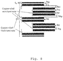
- Figure 8 shows another configuration of a twelve layer PCB.
- the primary side has three groups each comprising two layers, while the secondary side has two groups, each comprising three layers.
- Each group of three layers is constructed by forming two of the layers on either side of a substrate with the minimum designable thickness, h 11 , and then providing a layer of pre-preg with the minimum designable thickness, h 1p , between a metal layer formed on the substrate and a third metal layer.
- FIG. 7 and 8 are particularly suitable for high voltage applications, such as 400V applications where the isolation requirement is 5000V, for example, in which a larger designed spacing than 175 ⁇ m between layers on different sides of the transformer is required in order to meet the isolation requirements.
- the isolation material between all of the metal layers may be provided by pre-preg, the advantages of embodiments being realised by a thinner thickness of pre-preg being used between adjacent layers within a group.
- Figure 9 shows the operations performed in a method of manufacturing a multi-layered PCB according to an embodiment.
- the manufacturing process starts at step 901.
- step 903 a group of at least two conductive layers 6, 8, are formed, wherein adjacent conductive layers of the group are separated from each other by a layer of an isolation material.
- step 905 at least one conductive layer 16 above the group of conductive layers is formed, wherein the at least one conductive layer 16 is separated from a conductive layer of the group by a layer of isolation material.
- step 907 at least one further conductive layer 18 below the group of conductive layers is formed, wherein the at least one further conductive layer 18 is separated from a conductive layer of the group by a layer of isolation material.
- step 909 all of the conductive layers in the group of conductive layers 6, 8 are connected so that all of the conductive layers provide first windings.
- step 911 said at least one conductive layer 16 and said at least one further conductive layer 18 are connected to provide second windings.
- the thickness of the isolation material between at least a pair of adjacent conductive layers in the group of conductive layers 6, 8 of the first windings is less than the thickness of the isolation material between a conductive layer 16 of the second windings and a conductive layer 6 of the first windings.
- the groups of metal layers may comprise any number of layers and are not restricted to two, three or four as shown in Figures 5 to 8 .
- the total turns ratio of the transformer is determined by the number of parallel layers used and number of coils on each layer.
- the arrangement shown in Figure 5 may be designed to have a 4:1 turns ratio.
- the thermal transfer of the transformer is improved.
- the parasitic capacitive coupling between the primary and secondary sides is also reduced.
- the gain of the planar magnetic transformer according to embodiments is particularly large when adjacent layers of a group provide the same coil of a winding. By using two or more adjacent layers to provide the same coil, or turn, the resistance is decreased.
- the spacing between adjacent layers of a group may be provided by forming the metal layers on a substrate. This allows a lower isolation material thickness than that realisable with a pre-preg layer.
- the thickness of the isolation material has been reduced from 175 ⁇ m to 100 ⁇ m between adjacent layers within a group.
- the height of the PCB is about 10% less than the known arrangement shown in Figure 3 .
- the thermal resistance is also reduced by 18% without any increase in parasitic capacitance or leakage inductance.
- transformers with a lower height may be realised for a given power requirement.
- the embodiment shown in Figure 6 has a resistance that is 19% lower than the design shown in Figure 3 and also has a thermal resistance that is 18% lower. Accordingly, the transformer design according to the embodiment has about the same mechanical outer dimensions as the known transformer shown in Figure 3 but can operate at powers 20% higher. The improvement is provided by the thicker metal tracks resulting in lower resistance and also providing an improved thermal conductivity.
Landscapes
- Engineering & Computer Science (AREA)
- Power Engineering (AREA)
- Manufacturing & Machinery (AREA)
- Coils Or Transformers For Communication (AREA)
- Parts Printed On Printed Circuit Boards (AREA)
- Coils Of Transformers For General Uses (AREA)
- Production Of Multi-Layered Print Wiring Board (AREA)
Priority Applications (1)
| Application Number | Priority Date | Filing Date | Title |
|---|---|---|---|
| EP16195955.6A EP3147916A1 (de) | 2012-12-19 | 2012-12-19 | Verfahren zur herstellung eines planaren pcb transformators |
Applications Claiming Priority (3)
| Application Number | Priority Date | Filing Date | Title |
|---|---|---|---|
| EP12818994.1A EP2936513B1 (de) | 2012-12-19 | 2012-12-19 | Planarer transformator |
| PCT/EP2012/076119 WO2014094841A1 (en) | 2012-12-19 | 2012-12-19 | Planar transformer |
| EP16195955.6A EP3147916A1 (de) | 2012-12-19 | 2012-12-19 | Verfahren zur herstellung eines planaren pcb transformators |
Related Parent Applications (2)
| Application Number | Title | Priority Date | Filing Date |
|---|---|---|---|
| EP12818994.1A Division-Into EP2936513B1 (de) | 2012-12-19 | 2012-12-19 | Planarer transformator |
| EP12818994.1A Division EP2936513B1 (de) | 2012-12-19 | 2012-12-19 | Planarer transformator |
Publications (1)
| Publication Number | Publication Date |
|---|---|
| EP3147916A1 true EP3147916A1 (de) | 2017-03-29 |
Family
ID=47624001
Family Applications (2)
| Application Number | Title | Priority Date | Filing Date |
|---|---|---|---|
| EP16195955.6A Withdrawn EP3147916A1 (de) | 2012-12-19 | 2012-12-19 | Verfahren zur herstellung eines planaren pcb transformators |
| EP12818994.1A Not-in-force EP2936513B1 (de) | 2012-12-19 | 2012-12-19 | Planarer transformator |
Family Applications After (1)
| Application Number | Title | Priority Date | Filing Date |
|---|---|---|---|
| EP12818994.1A Not-in-force EP2936513B1 (de) | 2012-12-19 | 2012-12-19 | Planarer transformator |
Country Status (8)
| Country | Link |
|---|---|
| US (1) | US9576717B2 (de) |
| EP (2) | EP3147916A1 (de) |
| JP (1) | JP6170568B2 (de) |
| KR (1) | KR101735979B1 (de) |
| CN (1) | CN104854666B (de) |
| BR (1) | BR112015010157A2 (de) |
| WO (1) | WO2014094841A1 (de) |
| ZA (1) | ZA201503113B (de) |
Families Citing this family (20)
| Publication number | Priority date | Publication date | Assignee | Title |
|---|---|---|---|---|
| KR101443987B1 (ko) * | 2012-12-31 | 2014-09-23 | 삼성전기주식회사 | 반도체 모듈 패키지 |
| JP6267095B2 (ja) * | 2014-10-22 | 2018-01-24 | 株式会社大同工業所 | 防爆用安全保持器の積層トランス用のクリップ |
| CN105655113B (zh) | 2014-11-12 | 2018-04-17 | 台达电子工业股份有限公司 | Pcb平面变压器及使用这种变压器的变换器 |
| CN104575979A (zh) * | 2015-01-14 | 2015-04-29 | 南京新康达磁业股份有限公司 | 一种变压器或电感绕组结构 |
| KR20160134500A (ko) * | 2015-05-13 | 2016-11-23 | 페어차일드코리아반도체 주식회사 | 평면형 자기 소자 |
| CN105304296A (zh) * | 2015-11-04 | 2016-02-03 | 中国船舶重工集团公司第七二三研究所 | 一种印制电路板平面变压器 |
| DE102015222400A1 (de) * | 2015-11-13 | 2017-06-08 | Schaeffler Technologies AG & Co. KG | Multilayer-Platine und Verfahren zu deren Herstellung |
| CN107667407B (zh) * | 2016-05-31 | 2019-06-04 | 新电元工业株式会社 | 线圈构造体以及磁性部件 |
| JP2017220515A (ja) * | 2016-06-06 | 2017-12-14 | オムロンオートモーティブエレクトロニクス株式会社 | トランス |
| JP6624160B2 (ja) * | 2017-05-23 | 2019-12-25 | オムロン株式会社 | トランス一体型プリント基板 |
| CN107910170A (zh) * | 2017-11-10 | 2018-04-13 | 深圳市英大科特技术有限公司 | 一种饼式绕组高频变压器 |
| KR102174306B1 (ko) * | 2018-10-10 | 2020-11-04 | 이주열 | 성능 개선을 위한 절연 구조가 적용된 평면 트랜스포머 |
| US11189563B2 (en) * | 2019-08-01 | 2021-11-30 | Nanya Technology Corporation | Semiconductor structure and manufacturing method thereof |
| JP6906874B2 (ja) * | 2019-11-27 | 2021-07-21 | 三菱電機株式会社 | 電力変換装置 |
| WO2022064662A1 (ja) * | 2020-09-25 | 2022-03-31 | 住友電気工業株式会社 | トランス及びコンバータ |
| EP4081005A1 (de) | 2021-04-23 | 2022-10-26 | AT & S Austria Technologie & Systemtechnik Aktiengesellschaft | Komponententräger |
| CN114464437B (zh) * | 2022-01-17 | 2023-11-17 | 广州金升阳科技有限公司 | 一种磁性器件及其加工方法 |
| JP7760442B2 (ja) * | 2022-05-10 | 2025-10-27 | ルネサスエレクトロニクス株式会社 | 半導体装置 |
| US12609234B2 (en) | 2022-12-21 | 2026-04-21 | L3Harris Technologies, Inc. | Planar transformer |
| KR20260011460A (ko) * | 2024-07-16 | 2026-01-23 | 현대모비스 주식회사 | 평판형 변압기 |
Citations (4)
| Publication number | Priority date | Publication date | Assignee | Title |
|---|---|---|---|---|
| GB2295728A (en) * | 1994-12-02 | 1996-06-05 | Mtl Instr Group Plc | Transformers |
| US6054914A (en) * | 1998-07-06 | 2000-04-25 | Midcom, Inc. | Multi-layer transformer having electrical connection in a magnetic core |
| US20040145440A1 (en) * | 2003-01-28 | 2004-07-29 | Rantec Power Systems, Inc. | Integrated bobbin transformer assembly |
| CN201717110U (zh) * | 2010-05-21 | 2011-01-19 | 厦门安东电子有限公司 | 一种本质安全型平面变压器 |
Family Cites Families (33)
| Publication number | Priority date | Publication date | Assignee | Title |
|---|---|---|---|---|
| DE68925171T2 (de) * | 1988-09-30 | 1996-06-05 | Toshiba Kawasaki Kk | Planar-Induktivität |
| US5990776A (en) * | 1994-12-08 | 1999-11-23 | Jitaru; Ionel | Low noise full integrated multilayers magnetic for power converters |
| US5716713A (en) * | 1994-12-16 | 1998-02-10 | Ceramic Packaging, Inc. | Stacked planar transformer |
| JP3336923B2 (ja) * | 1997-08-26 | 2002-10-21 | 株式会社日立製作所 | 変圧器巻線およびその製造方法 |
| IE990428A1 (en) * | 1998-05-26 | 2001-01-10 | Artesyn Tech | A transformer assembly |
| MY144503A (en) * | 1998-09-14 | 2011-09-30 | Ibiden Co Ltd | Printed circuit board and method for its production |
| US6198374B1 (en) * | 1999-04-01 | 2001-03-06 | Midcom, Inc. | Multi-layer transformer apparatus and method |
| JP2002057543A (ja) * | 2000-08-09 | 2002-02-22 | Murata Mfg Co Ltd | 積層型lc部品 |
| EP1340234A1 (de) * | 2000-11-21 | 2003-09-03 | Koninklijke Philips Electronics N.V. | System, leiterplatte, ladegerät, benutzergerät und vorrichtung |
| JP2004040025A (ja) * | 2002-07-08 | 2004-02-05 | Natl Space Development Agency Of Japan | シート型トランス及び電子機器 |
| US6914508B2 (en) * | 2002-08-15 | 2005-07-05 | Galaxy Power, Inc. | Simplified transformer design for a switching power supply |
| US7012481B2 (en) * | 2002-10-04 | 2006-03-14 | Matsushita Electric Industrial Co., Ltd. | Duplexer, and laminate-type high-frequency device and communication equipment using the same |
| JP2007523574A (ja) * | 2004-02-23 | 2007-08-16 | ジョージア テック リサーチ コーポレイション | 液晶性ポリマー及び多層ポリマーベースの無線周波/無線マルチバンド用途の受動信号処理コンポーネント |
| US7248138B2 (en) * | 2004-03-08 | 2007-07-24 | Astec International Limited | Multi-layer printed circuit board inductor winding with added metal foil layers |
| US7292126B2 (en) * | 2004-04-30 | 2007-11-06 | Astec International Limited | Low noise planar transformer |
| WO2006033071A1 (en) * | 2004-09-24 | 2006-03-30 | Philips Intellectual Property & Standards Gmbh | Transformer |
| JP4769033B2 (ja) * | 2005-03-23 | 2011-09-07 | スミダコーポレーション株式会社 | インダクタ |
| JP2009519578A (ja) * | 2005-12-16 | 2009-05-14 | コーニンクレッカ フィリップス エレクトロニクス エヌ ヴィ | 高電圧変圧器 |
| US7671706B2 (en) * | 2006-04-14 | 2010-03-02 | Murata Manufacturing Co., Ltd | High frequency multilayer bandpass filter |
| US7791900B2 (en) * | 2006-08-28 | 2010-09-07 | Avago Technologies General Ip (Singapore) Pte. Ltd. | Galvanic isolator |
| US9105391B2 (en) * | 2006-08-28 | 2015-08-11 | Avago Technologies General Ip (Singapore) Pte. Ltd. | High voltage hold-off coil transducer |
| FR2911992A1 (fr) * | 2007-01-30 | 2008-08-01 | St Microelectronics Sa | Inductance multiniveaux |
| WO2008152616A1 (en) * | 2007-06-11 | 2008-12-18 | Moog Limited | Low-profile transformer |
| JP2009016504A (ja) * | 2007-07-03 | 2009-01-22 | Shinko Electric Ind Co Ltd | インダクタ内蔵型多層配線基板 |
| JP5194946B2 (ja) * | 2008-03-28 | 2013-05-08 | 富士通株式会社 | ネットワーク接続装置、および当該装置における信号処理方法 |
| US8258911B2 (en) * | 2008-03-31 | 2012-09-04 | Avago Technologies ECBU IP (Singapor) Pte. Ltd. | Compact power transformer components, devices, systems and methods |
| JP2009259922A (ja) * | 2008-04-15 | 2009-11-05 | Mitsubishi Electric Corp | 平面型電磁誘導電器 |
| TWI398984B (zh) * | 2008-05-23 | 2013-06-11 | Murata Manufacturing Co | Laminated bandpass filter |
| US8598719B2 (en) * | 2008-06-12 | 2013-12-03 | Sumitomo Bakelite Company Limited | Semiconductor element mounting board |
| CN102474979B (zh) | 2009-09-01 | 2015-01-07 | 株式会社丰田自动织机 | 电路基板的制造方法以及电路基板 |
| DE102009057788A1 (de) | 2009-12-11 | 2011-06-22 | Krohne Messtechnik GmbH, 47058 | Planartransformator |
| JP2012134291A (ja) * | 2010-12-21 | 2012-07-12 | Sanken Electric Co Ltd | 電子回路装置 |
| US8674418B2 (en) * | 2011-08-19 | 2014-03-18 | National Semiconductor Corporation | Method and apparatus for achieving galvanic isolation in package having integral isolation medium |
-
2012
- 2012-12-19 WO PCT/EP2012/076119 patent/WO2014094841A1/en not_active Ceased
- 2012-12-19 JP JP2015548222A patent/JP6170568B2/ja not_active Expired - Fee Related
- 2012-12-19 BR BR112015010157A patent/BR112015010157A2/pt not_active Application Discontinuation
- 2012-12-19 EP EP16195955.6A patent/EP3147916A1/de not_active Withdrawn
- 2012-12-19 KR KR1020157018559A patent/KR101735979B1/ko not_active Expired - Fee Related
- 2012-12-19 CN CN201280077889.2A patent/CN104854666B/zh not_active Expired - Fee Related
- 2012-12-19 EP EP12818994.1A patent/EP2936513B1/de not_active Not-in-force
- 2012-12-19 US US13/810,288 patent/US9576717B2/en not_active Expired - Fee Related
-
2015
- 2015-05-06 ZA ZA2015/03113A patent/ZA201503113B/en unknown
Patent Citations (4)
| Publication number | Priority date | Publication date | Assignee | Title |
|---|---|---|---|---|
| GB2295728A (en) * | 1994-12-02 | 1996-06-05 | Mtl Instr Group Plc | Transformers |
| US6054914A (en) * | 1998-07-06 | 2000-04-25 | Midcom, Inc. | Multi-layer transformer having electrical connection in a magnetic core |
| US20040145440A1 (en) * | 2003-01-28 | 2004-07-29 | Rantec Power Systems, Inc. | Integrated bobbin transformer assembly |
| CN201717110U (zh) * | 2010-05-21 | 2011-01-19 | 厦门安东电子有限公司 | 一种本质安全型平面变压器 |
Also Published As
| Publication number | Publication date |
|---|---|
| WO2014094841A1 (en) | 2014-06-26 |
| KR20150095820A (ko) | 2015-08-21 |
| KR101735979B1 (ko) | 2017-05-29 |
| EP2936513B1 (de) | 2017-02-15 |
| BR112015010157A2 (pt) | 2017-07-11 |
| US9576717B2 (en) | 2017-02-21 |
| US20140167901A1 (en) | 2014-06-19 |
| ZA201503113B (en) | 2016-08-31 |
| JP6170568B2 (ja) | 2017-07-26 |
| JP2016506624A (ja) | 2016-03-03 |
| CN104854666B (zh) | 2018-03-30 |
| EP2936513A1 (de) | 2015-10-28 |
| CN104854666A (zh) | 2015-08-19 |
Similar Documents
| Publication | Publication Date | Title |
|---|---|---|
| EP2936513B1 (de) | Planarer transformator | |
| US12568586B2 (en) | Inductor assembly and manufacturing method for inductor assembly | |
| US6674355B2 (en) | Slot core transformers | |
| EP2156447B1 (de) | Transformator mit niedrigem profil | |
| EP0917163B1 (de) | Magnetische Baugruppe | |
| CN103430252B (zh) | 层叠型电感元件及其制造方法 | |
| US20040174241A1 (en) | Planar transformer and output inductor structure with single planar winding board and two magnetic cores | |
| US9007144B2 (en) | Multilayer power splitter | |
| CN1575500A (zh) | 多层电路及其制造方法 | |
| CN103443879B (zh) | 层叠型电感元件及其制造方法 | |
| JP6048509B2 (ja) | 積層型インダクタ素子 | |
| JP2017220515A (ja) | トランス | |
| US11424066B2 (en) | Electronic component including planar transformer | |
| US6551426B2 (en) | Manufacturing method for a laminated ceramic electronic component | |
| US20020163818A1 (en) | Magnetic device and method of manufacture therefor | |
| US20250378987A1 (en) | Integrated transformer and inductor assembly with fractional windings | |
| US12469631B2 (en) | Power supply module | |
| JPH09219324A (ja) | 線輪部品およびその製造方法 | |
| KR20140084970A (ko) | 적층형 칩 인덕터 | |
| WO2014030471A1 (ja) | 積層基板およびその製造方法 | |
| JP2026513294A (ja) | 誘導コイルアセンブリおよびその製造方法 | |
| JP4389441B2 (ja) | 薄形積層トランスの製造方法 | |
| CN121727374A (zh) | 一种基于对称式llc谐振腔变换器 | |
| JP2011071320A (ja) | トランス | |
| WO2005043566A1 (ja) | 積層型磁性部品及びその製造方法並びに積層型磁性部品用積層体の製造方法 |
Legal Events
| Date | Code | Title | Description |
|---|---|---|---|
| PUAI | Public reference made under article 153(3) epc to a published international application that has entered the european phase |
Free format text: ORIGINAL CODE: 0009012 |
|
| AC | Divisional application: reference to earlier application |
Ref document number: 2936513 Country of ref document: EP Kind code of ref document: P |
|
| AK | Designated contracting states |
Kind code of ref document: A1 Designated state(s): AL AT BE BG CH CY CZ DE DK EE ES FI FR GB GR HR HU IE IS IT LI LT LU LV MC MK MT NL NO PL PT RO RS SE SI SK SM TR |
|
| 17P | Request for examination filed |
Effective date: 20170705 |
|
| RBV | Designated contracting states (corrected) |
Designated state(s): AL AT BE BG CH CY CZ DE DK EE ES FI FR GB GR HR HU IE IS IT LI LT LU LV MC MK MT NL NO PL PT RO RS SE SI SK SM TR |
|
| STAA | Information on the status of an ep patent application or granted ep patent |
Free format text: STATUS: THE APPLICATION HAS BEEN WITHDRAWN |
|
| 18W | Application withdrawn |
Effective date: 20190124 |