EP3147932A1 - Générateur de tension haute fréquence - Google Patents
Générateur de tension haute fréquence Download PDFInfo
- Publication number
- EP3147932A1 EP3147932A1 EP14892614.0A EP14892614A EP3147932A1 EP 3147932 A1 EP3147932 A1 EP 3147932A1 EP 14892614 A EP14892614 A EP 14892614A EP 3147932 A1 EP3147932 A1 EP 3147932A1
- Authority
- EP
- European Patent Office
- Prior art keywords
- voltage
- direct
- radio
- frequency
- current voltage
- Prior art date
- Legal status (The legal status is an assumption and is not a legal conclusion. Google has not performed a legal analysis and makes no representation as to the accuracy of the status listed.)
- Granted
Links
- 230000001052 transient effect Effects 0.000 claims abstract description 84
- 239000003990 capacitor Substances 0.000 claims description 43
- 238000005040 ion trap Methods 0.000 claims description 3
- 150000002500 ions Chemical class 0.000 description 34
- 238000010884 ion-beam technique Methods 0.000 description 20
- 230000014759 maintenance of location Effects 0.000 description 12
- 239000002245 particle Substances 0.000 description 9
- 238000010586 diagram Methods 0.000 description 5
- 238000006243 chemical reaction Methods 0.000 description 4
- 238000000034 method Methods 0.000 description 3
- 230000000717 retained effect Effects 0.000 description 2
- 238000011144 upstream manufacturing Methods 0.000 description 2
- 230000005540 biological transmission Effects 0.000 description 1
- 230000015572 biosynthetic process Effects 0.000 description 1
- 230000000694 effects Effects 0.000 description 1
- 238000001914 filtration Methods 0.000 description 1
- 230000010355 oscillation Effects 0.000 description 1
- 230000002441 reversible effect Effects 0.000 description 1
- 230000002123 temporal effect Effects 0.000 description 1
Images



Classifications
-
- H—ELECTRICITY
- H01—ELECTRIC ELEMENTS
- H01J—ELECTRIC DISCHARGE TUBES OR DISCHARGE LAMPS
- H01J49/00—Particle spectrometers or separator tubes
- H01J49/02—Details
- H01J49/06—Electron- or ion-optical arrangements
- H01J49/062—Ion guides
-
- H—ELECTRICITY
- H02—GENERATION; CONVERSION OR DISTRIBUTION OF ELECTRIC POWER
- H02M—APPARATUS FOR CONVERSION BETWEEN AC AND AC, BETWEEN AC AND DC, OR BETWEEN DC AND DC, AND FOR USE WITH MAINS OR SIMILAR POWER SUPPLY SYSTEMS; CONVERSION OF DC OR AC INPUT POWER INTO SURGE OUTPUT POWER; CONTROL OR REGULATION THEREOF
- H02M7/00—Conversion of AC power input into DC power output; Conversion of DC power input into AC power output
- H02M7/42—Conversion of DC power input into AC power output without possibility of reversal
- H02M7/44—Conversion of DC power input into AC power output without possibility of reversal by static converters
- H02M7/48—Conversion of DC power input into AC power output without possibility of reversal by static converters using discharge tubes with control electrode or semiconductor devices with control electrode
- H02M7/53—Conversion of DC power input into AC power output without possibility of reversal by static converters using discharge tubes with control electrode or semiconductor devices with control electrode using devices of a triode or transistor type requiring continuous application of a control signal
- H02M7/537—Conversion of DC power input into AC power output without possibility of reversal by static converters using discharge tubes with control electrode or semiconductor devices with control electrode using devices of a triode or transistor type requiring continuous application of a control signal using semiconductor devices only, e.g. single switched pulse inverters
- H02M7/538—Conversion of DC power input into AC power output without possibility of reversal by static converters using discharge tubes with control electrode or semiconductor devices with control electrode using devices of a triode or transistor type requiring continuous application of a control signal using semiconductor devices only, e.g. single switched pulse inverters in a push-pull configuration
-
- H—ELECTRICITY
- H01—ELECTRIC ELEMENTS
- H01J—ELECTRIC DISCHARGE TUBES OR DISCHARGE LAMPS
- H01J49/00—Particle spectrometers or separator tubes
- H01J49/26—Mass spectrometers or separator tubes
- H01J49/34—Dynamic spectrometers
- H01J49/42—Stability-of-path spectrometers, e.g. monopole, quadrupole, multipole, farvitrons
- H01J49/4205—Device types
- H01J49/422—Two-dimensional RF ion traps
-
- H—ELECTRICITY
- H02—GENERATION; CONVERSION OR DISTRIBUTION OF ELECTRIC POWER
- H02M—APPARATUS FOR CONVERSION BETWEEN AC AND AC, BETWEEN AC AND DC, OR BETWEEN DC AND DC, AND FOR USE WITH MAINS OR SIMILAR POWER SUPPLY SYSTEMS; CONVERSION OF DC OR AC INPUT POWER INTO SURGE OUTPUT POWER; CONTROL OR REGULATION THEREOF
- H02M7/00—Conversion of AC power input into DC power output; Conversion of DC power input into AC power output
- H02M7/42—Conversion of DC power input into AC power output without possibility of reversal
- H02M7/44—Conversion of DC power input into AC power output without possibility of reversal by static converters
-
- H—ELECTRICITY
- H02—GENERATION; CONVERSION OR DISTRIBUTION OF ELECTRIC POWER
- H02M—APPARATUS FOR CONVERSION BETWEEN AC AND AC, BETWEEN AC AND DC, OR BETWEEN DC AND DC, AND FOR USE WITH MAINS OR SIMILAR POWER SUPPLY SYSTEMS; CONVERSION OF DC OR AC INPUT POWER INTO SURGE OUTPUT POWER; CONTROL OR REGULATION THEREOF
- H02M7/00—Conversion of AC power input into DC power output; Conversion of DC power input into AC power output
- H02M7/42—Conversion of DC power input into AC power output without possibility of reversal
- H02M7/44—Conversion of DC power input into AC power output without possibility of reversal by static converters
- H02M7/48—Conversion of DC power input into AC power output without possibility of reversal by static converters using discharge tubes with control electrode or semiconductor devices with control electrode
- H02M7/4815—Resonant converters
-
- Y—GENERAL TAGGING OF NEW TECHNOLOGICAL DEVELOPMENTS; GENERAL TAGGING OF CROSS-SECTIONAL TECHNOLOGIES SPANNING OVER SEVERAL SECTIONS OF THE IPC; TECHNICAL SUBJECTS COVERED BY FORMER USPC CROSS-REFERENCE ART COLLECTIONS [XRACs] AND DIGESTS
- Y02—TECHNOLOGIES OR APPLICATIONS FOR MITIGATION OR ADAPTATION AGAINST CLIMATE CHANGE
- Y02B—CLIMATE CHANGE MITIGATION TECHNOLOGIES RELATED TO BUILDINGS, e.g. HOUSING, HOUSE APPLIANCES OR RELATED END-USER APPLICATIONS
- Y02B70/00—Technologies for an efficient end-user side electric power management and consumption
- Y02B70/10—Technologies improving the efficiency by using switched-mode power supplies [SMPS], i.e. efficient power electronics conversion e.g. power factor correction or reduction of losses in power supplies or efficient standby modes
Definitions
- the present invention relates to a radio-frequency voltage generator that generates radio-frequency voltage from direct-current voltage and applies the radio-frequency voltage to a load.
- the radio-frequency voltage generator is suitably used in a charged particle controller such as an ion guide and an ion trap to control focusing, transportation, and filtering on ions in a mass spectrometer.
- a charged particle controller used in a mass spectrometer uses a radiofrequency field that is spatially and temporally modulated to control the movement of ions (see Patent Literature 1).
- a radio-frequency voltage V RF having an amplitude of V and a frequency of ⁇ is applied so that adjacent rod electrodes have reversed polarity, whereby a pseudopotential V p (R) due to the radiofrequency field is formed in the ion guide.
- V RF denotes a distance from the ion beam axis in a radial direction.
- the pseudopotential V p (R) changes. Therefore, making the pseudopotential V p (R) change along the ion beam axis forms a gradient of the pseudopotential V p (R), and force is generated by the gradient, whereby ions can be transported.
- electrodes arranged separately in the direction of the ion beam axis may be used instead of a simple rod electrode, and radio-frequency voltages V RF having different amplitudes V and frequencies ⁇ may be applied to the respective electrodes.
- V RF radio-frequency voltages
- a complicated device has to be used, which is difficult to be implemented for ion guides.
- a digital radio-frequency voltage generator that generates rectangular waves is used, in which a direct-current voltage is switched on/off at high speed or positive/negative direct-current voltages are alternately switched at high-speed to generate (pseudo-)radio-frequency voltage.
- a typical digital radio-frequency voltage generator performs a switching operation in which the positive/negative direct-current voltages are alternately repeated ( Fig. 9A ).
- Patent Literature 2 describes that the direct-current voltage is set at 0 for a certain time period when the direct-current voltage is switched from positive to negative, and from negative to positive, that is, the direct-current voltage is switched in the order of 0 ⁇ +V 0 ⁇ 0 ⁇ -V 0 ⁇ 0 during one cycle of a radio frequency ( Fig. 9B ).
- the ratio of a time period t v to maintain the direct-current voltage at +V 0 and -V 0 to a time period to to maintain the direct-current voltage at zero, it is possible to change the effective amplitude V of the radio-frequency voltage without changing the cycle and the magnitude of the direct-current voltage.
- Switching of voltages illustrated in Fig. 9B is implemented by, for example, an electric circuit 90 illustrated in Fig. 10 .
- a capacitor C in the electric circuit 90 corresponds to an electrode pair in an ion guide.
- One of the terminals of the capacitor C is grounded, and the other terminal is connected in parallel to a first power supply E 1 at a potential +V 0 via a first switch S 1 and a second power supply E 2 at a potential -V 0 via a second switch S 2 .
- an electric resistance R and a zeroth switch So which are connected in series to each other, are connected in parallel to the capacitor C.
- the switching of voltage in the electric circuit 90 is performed as follows. With the zeroth switch S 0 connected in parallel to the capacitor C (electrode pair) being opened, the second switch S 2 is opened, and the first switch S 1 is closed, whereby a voltage +V 0 is applied across the capacitor C (electrode pair) ( Fig. 11A ). Next, the first switch S 1 is opened, and the zeroth switch S 0 is closed, whereby the voltage across the capacitor C (electrode pair) becomes zero ( Fig. 11B ). Subsequently, the zeroth switch S 0 is opened, and the second switch S 2 is closed, whereby the voltage -V 0 is applied across the capacitor C (electrode pair) ( Fig. 11C ).
- the second switch S 2 is opened, and the zeroth switch S 0 is closed, whereby the voltage across the capacitor C (electrode pair) becomes zero ( Fig. 11D ).
- the switching of voltages, 0 ⁇ +V 0 ⁇ 0 ⁇ -V 0 ⁇ 0, that is one cycle of the radio-frequency voltage is performed.
- the effective amplitude V of the radio-frequency voltage can be controlled.
- This circuit is simpler than that in the case of using an analog (sine wave) radio frequency and can be easily implemented.
- the waveform is rectangular, and voltage is sharply changed at the time of switching the direct-current voltages, causing electrical noise.
- electric charges accumulated in the capacitor C flow through the electric resistance R at the time of changing the voltage from ⁇ V 0 to 0, where electric power is consumed.
- the matter to be achieved by the present invention is to provide a radio-frequency voltage generator capable of suppressing the occurrence of noise and the consumption of electric power.
- the present invention which has been made to solve the above problems, is a radio-frequency voltage generator that generates radio-frequency voltage from direct-current voltage and applies the radio-frequency voltage to a load, the radio-frequency voltage generator including:
- radio-frequency voltage generator basically, (pseudo-)radio-frequency voltage is generated by applying the first direct-current voltage and the second direct-current voltage to the load alternately.
- a transient alternating voltage is applied to the load, the transient alternating voltage having a maximum value that is one of the first direct-current voltage and the second direct-current voltage, and a minimum value that is the other one.
- the transient alternating voltage is caused to oscillate a half-integer times starting with an initial value being the direct-current voltage that is applied to the load immediately before the application of the transient alternating voltage, the half-integer being equal to or greater than 1.5, namely, the transient alternating voltage is caused to oscillate one or more times and further oscillate a half times, whereby the transient alternating voltage can be switched from the first direct-current voltage to the second direct-current voltage or from the second direct-current voltage to the first direct-current voltage before and after the application of the transient alternating voltage.
- the direct-current voltages can be gently switched as compared with a conventional radio-frequency voltage generator using a rectangular wave, whereby it is possible to suppress the occurrence of noise.
- switching the first direct-current voltage and the second direct-current voltage with the transient alternating voltage interposed therebetween need not an electric resistance that is a cause of the loss of electric power.
- the radio-frequency voltage generator can include an effective amplitude change section for changing the ratio of a time period for which the first direct-current voltage and the second direct-current voltage is applied to a time period for which the transient alternating voltage is applied.
- an effective amplitude change section for changing the ratio of a time period for which the first direct-current voltage and the second direct-current voltage is applied to a time period for which the transient alternating voltage is applied.
- the radio-frequency voltage generator according to the present invention can further include a radio-frequency voltage frequency change section for changing one or both of the time period for which the first direct-current voltage and the second direct-current voltage is applied, and the time period for which the transient alternating voltage is applied. With this configuration, the frequency of the radio-frequency voltage can be changed only by changing these time periods.
- the transient alternating voltage generator is an LC circuit including an inductor and a capacitor connected in series to each other, and that further includes an LC circuit make-and-break section for making and breaking the LC circuit, and a direct-current voltage selective application section for selectively applying the first direct-current voltage or the second direct-current voltage to the capacitor.
- the transient alternating voltage generator having such a configuration, when the voltage switch section switches from the direct-current voltage being one of the first direct-current voltage and the second direct-current voltage to the transient alternating voltage, the LC circuit make-and-break section breaks the LC circuit, and then the direct-current voltage selective application section applies the one direct-current voltage to the capacitor.
- the direct-current voltage selective application section ends the application of the one direct-current voltage, and then the LC circuit make-and-break section makes the LC circuit.
- This causes an alternate-current (AC) voltage having the initial value being the one direct-current voltage, namely the direct-current voltage applied immediately before the application of the transient alternating voltage to generate across the capacitor. Therefore, the voltage across the capacitor may be output as the transient alternating voltage to be applied to the load.
- the load constitutes the capacitor, the load itself may be provided as the capacitor of the LC circuit.
- the radio-frequency voltage generator according to the present invention can be preferably used to supply radio-frequency voltages to a charged particle controller used in a mass spectrometer.
- the radio-frequency voltage generator can be used for supplying the radio-frequency voltage V RF to be applied to the electrodes.
- the radio-frequency voltage generator including the effective amplitude change section can be preferably used in that the pseudopotential V p (R) in the ion guide can be easily controlled by changing the amplitude of the radio-frequency voltage V RF .
- separate radio-frequency voltage generators may be used for individual electrodes arranged in the direction of the ion beam axis, and the radio-frequency voltages having different amplitudes may be applied to electrodes from the respective radio-frequency voltage generators.
- the waveform of the transient alternating voltage is contained in the waveform of the intended radio-frequency voltage.
- the frequency of the transient alternating voltage is made sufficiently high, charged particles are difficult to follow temporal changes in force exerted by the transient alternating voltage, and thus the transient alternating voltage will have no influence on the control of the charged particles.
- a radio-frequency filter having a cut-off frequency higher than the frequency ⁇ of the radio-frequency voltage and lower than the frequency ⁇ of the transient alternating voltage the influence of the transient alternating voltage can be also eliminated.
- the radio-frequency voltage generator according to the present invention is also applicable to a device other than the charged particle controller.
- a DC-DC converter converting the value of direct-current voltage, with the first direct-current voltage set at the direct-current voltage before the conversion and the second direct-current voltage set at zero, a high-frequency current having a voltage oscillating between the direct-current voltage before the conversion and zero is generated by the radio-frequency voltage generator according to the present invention, and thereafter the high-frequency current is rectified to direct current (DC), whereby a direct-current having a voltage different from that before the conversion is output.
- DC direct current
- the direct-current voltage on the output side can be controlled.
- the radio-frequency voltage generator by applying the transient alternating voltage during switching between the first direct-current voltage and the second direct-current voltage, the voltage can be gently switched as compared with a conventional radio-frequency voltage generator using a rectangular wave, whereby it is possible to suppress the occurrence of noise.
- switching the first direct-current voltage and the second direct-current voltage with the transient alternating voltage interposed therebetween need not an electric resistance that is a cause of the loss of electric power.
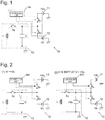
- a radio-frequency voltage generator 10 includes an electric circuit illustrated in Fig. 1 .
- the radio-frequency voltage generator 10 is configured to supply radio-frequency voltage to an ion guide used in a mass spectrometer, and a capacitor C of the electric circuit is equivalent to an electrode pair in the ion guide.
- the radio-frequency voltage generator 10 includes a first direct-current (DC) power supply 11, a second direct-current (DC) power supply 12, a transient alternating voltage generation circuit 13, and a voltage switch section 14.
- the first DC power supply 11 corresponds to the first direct-current voltage generation section
- the second DC power supply 12 corresponds to the second direct-current voltage generation section
- the transient alternating voltage generation circuit 13 corresponds to the transient alternating voltage generation section.
- One of the terminals of the capacitor C (electrode pair) is grounded, and the other terminal is connected in parallel to a first power supply E 1 at a potential +V 0 via a first switch S 1 and a second power supply E 2 at a potential -V 0 via a second switch S 2 .
- a coil L and a zeroth switch S 0 which are connected in series to each other, are connected in parallel to the capacitor C (electrode pair).
- the LC circuit will be referred to as the transient alternating voltage generation circuit 13.
- the resonance frequency of the transient alternating voltage generation circuit 13 will be denoted by ⁇ for distinction from a frequency ⁇ of the radio-frequency voltage generated by the radio-frequency voltage generator 10.
- the inductance of the coil L is set so that the resonance frequency ⁇ of the transient alternating voltage generation circuit 13 becomes sufficiently higher than the frequency ⁇ of the radio-frequency voltage (e.g. ten or more times).
- the voltage switch section 14 includes the zeroth switch So, the first switch S 1 and the second switch S 2 , as well as a controlling unit 141 configured to perform control of opening/closing these three switches.
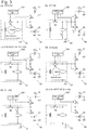
- a positive direct-current voltage +V 0 is applied in the following manner.
- the controlling unit 141 transmits a predetermined control signal to the first switch S 1 to close the first switch S 1 ( Fig. 2(1) ).
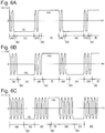
- This operation causes the voltage of the capacitor C (electrode pair) to rise to +V 0 (the period illustrated in Fig. 4 by reference numeral (1), which will be hereafter simply referred to as Fig. 4(1) or the like).
- the first switch S 1 is opened ( Fig. 2(2) ), which retains an initial state where the positive direct-current voltage +V 0 is applied to the capacitor C (electrode pair) ( Fig. 4(2) ).
- the zeroth switch S 0 is closed ( Fig. 3(a) ).
- This causes resonance current to flow through the LC circuit, and a transient alternating voltage is applied to the capacitor C (electrode pair), the transient alternating voltage having an initial value of +V 0 , maximum value of +V 0 , a minimum value of -V 0 , and a frequency of ⁇ ( Fig. 4(a) ).
- This transient alternating voltage is applied for a time period during which the transient alternating voltage oscillates a half-integer of times (1.5 or more times), namely the transient alternating voltage oscillates one or more times and further oscillates a half times (hereafter, referred to as a transient alternating voltage application time period).
- the time period may be controlled based on the clock frequency of a CPU included in the controlling unit 141 after calculating the frequency ⁇ in advance.
- a frequency counter for detecting the oscillation of the voltage may be provided in the LC circuit, and the timing to end the application of the transient alternating voltage may be determined based on the number of counts.
- the voltage applied to the capacitor C (electrode pair) theoretically becomes a voltage -V 0 , namely the reverse of a voltage +V 0 that is a voltage immediately before the application of the transient alternating voltage.
- the LC circuit has an internal resistance, and thus, as illustrated in Fig. 5 , the voltage applied to the capacitor C (electrode pair) actually attenuates to -(V 0 - ⁇ ) the absolute value of which is slightly smaller than that of -V 0 . In Fig. 5 , the attenuation is enhanced than actual for convenience of illustration.
- the second switch S 2 is opened ( Fig. 3(c) ), and this state is retained for a predetermined time period (hereafter, referred to as a direct-current voltage retention time period) ( Fig. 4(c) ).
- the predetermined time period is set so that the total of the predetermined time period, the transient alternating voltage application time period ( Fig. 4(a) ), and a time period to apply a negative direct-current voltage -V 0 ( Fig. 4(b) ) becomes a half cycle of the radio-frequency voltage.
- the direct-current voltage retention time period is controlled based on the clock frequency of the CPU of the controlling unit 141.
- the zeroth switch S 0 is closed ( Fig. 3(d) ), whereby the resonance current flows through the LC circuit again, and a transient alternating voltage is applied to the capacitor C (electrode pair), the transient alternating voltage having an initial value of -V 0 , a minimum value of -V 0 , a maximum value of +V 0 , and a frequency of ⁇ ( Fig. 4(d) ). Then, by applying this transient alternating voltage for the transient alternating voltage application time period, the voltage applied to the capacitor C (electrode pair) is reversed from -V 0 to +V 0 (strictly, +(V 0 - ⁇ )).
- the zeroth switch S 0 is opened and the first switch S 1 is closed ( Fig. 3(e) ), whereby the direct-current voltage applied to the capacitor C (electrode pair) is adjusted to +V 0 ( Fig. 4(e) ). Then, the first switch S 1 is opened ( Fig. 3(f) ), and this state is retained for the direct-current voltage retention time period ( Fig. 4(f) ).
- the radio-frequency voltage is applied to the capacitor C (electrode pair) by one cycle. Afterward, the above operation is repeated and the radio-frequency voltage is continuously applied to the capacitor C (electrode pair).
- the radio-frequency voltage generator 10 by applying the transient alternating voltage to the capacitor C (electrode pair) at the time of switching from the positive direct-current voltage +V 0 to the negative direct-current voltage -V 0 , and at the time of switching from the negative direct-current voltage - Vo to the positive direct-current voltage, the voltage can be gently switched as compared with a conventional radio-frequency voltage generator using a rectangular wave, whereby it is possible to suppress the occurrence of noise and the loss of electric power.
- the radio-frequency voltage generator 10 by changing the ratio of the direct-current voltage retention time period to the transient alternating voltage application time period, it is possible to control the effective magnitude of the radio-frequency voltage applied to the capacitor C (electrode pair).
- the ratio of the direct-current voltage retention time period ((c), (f)) to the transient alternating voltage application time period ((a), (d)) becomes small in the order of Fig. 6A, Fig. 6B, and Fig. 6C , the effective magnitude of the radio-frequency voltage also becomes small in this order.
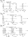
- the radio-frequency voltage generator 10 by changing the direct-current voltage retention time period and/or the transient alternating voltage application time period, it is possible to control the frequency of the radio-frequency voltage applied to the capacitor C (electrode pair).
- the transient alternating voltage application time period is the same, but the latter has a direct-current voltage retention time period longer than that of the former, and accordingly, the latter has a frequency of the radio-frequency voltage lower than that of the former.
- the direct-current voltage retention time period is the same, but the latter has a transient alternating voltage application time period longer than that of the former, and accordingly, the latter has a frequency of the radio-frequency voltage lower than that of the former.
- both of the direct-current voltage retention time period and the transient alternating voltage application time period may be changed.
- an example of an ion guide including the radio-frequency voltage generator 10 according to the present embodiment will be described.
- an ion guide 20 eight sets of electrodes are arranged around ion beam axis 29 at regular intervals, where a set of electrodes include rods separately arranged in the direction of an ion beam axis 29 at regular intervals.
- Five electrodes arranged in the direction of the ion beam axis 29 are denoted by reference signs 2xa, 2xb, 2xc, 2xd, and 2xe.
- x denotes a number from 1 to 8 attached correspondingly to the eight sets of electrodes arranged around the ion beam axis 29 in the arrangement order.
- the radio-frequency voltage generator 10 according to the present embodiment is provided for each eight electrodes lying in the same position in the direction of ion beam axis 29.
- a radio-frequency voltage V RF1 is applied between electrodes each having x being an odd number and electrodes each having x being an even number, using a radio-frequency voltage generator 10a.
- radio-frequency voltages V RF2 , V RF3 , V RF4 , V RF5 are applied between electrodes each having x being an odd number and electrodes each having x being an even number.
- a DC bias voltage V Bias is applied while superimposed on the radio-frequency voltages.
- this ion guide 20 by making the amplitudes of the radio-frequency voltages in the order of
- a similar pseudopotential is formed in the ion guide 20. Owing to the formation of the pseudopotential in such a manner, the ion guide 20 moves positive ions toward the direction of the ion beam axis.
- the radio-frequency voltage generator 10 is also applicable to a charged particle controller other than an ion guide in a mass spectrometer, such as an ion trap and a mass filter.
- the radio-frequency voltage generator 10 is also applicable to a device other than a charged particle controller, such as a device that generates radio-frequency voltage from direct-current voltage in the process of voltage conversion in a DC-DC converter.
Landscapes
- Engineering & Computer Science (AREA)
- Power Engineering (AREA)
- Chemical & Material Sciences (AREA)
- Analytical Chemistry (AREA)
- Dc-Dc Converters (AREA)
- Electron Tubes For Measurement (AREA)
- Other Investigation Or Analysis Of Materials By Electrical Means (AREA)
Applications Claiming Priority (1)
| Application Number | Priority Date | Filing Date | Title |
|---|---|---|---|
| PCT/JP2014/063475 WO2015177886A1 (fr) | 2014-05-21 | 2014-05-21 | Générateur de tension haute fréquence |
Publications (3)
| Publication Number | Publication Date |
|---|---|
| EP3147932A1 true EP3147932A1 (fr) | 2017-03-29 |
| EP3147932A4 EP3147932A4 (fr) | 2017-06-07 |
| EP3147932B1 EP3147932B1 (fr) | 2018-04-25 |
Family
ID=54553582
Family Applications (1)
| Application Number | Title | Priority Date | Filing Date |
|---|---|---|---|
| EP14892614.0A Not-in-force EP3147932B1 (fr) | 2014-05-21 | 2014-05-21 | Générateur de tension haute fréquence |
Country Status (5)
| Country | Link |
|---|---|
| US (1) | US9773655B2 (fr) |
| EP (1) | EP3147932B1 (fr) |
| JP (1) | JP6191766B2 (fr) |
| CN (1) | CN106463333B (fr) |
| WO (1) | WO2015177886A1 (fr) |
Families Citing this family (1)
| Publication number | Priority date | Publication date | Assignee | Title |
|---|---|---|---|---|
| WO2018211611A1 (fr) * | 2017-05-17 | 2018-11-22 | 株式会社島津製作所 | Dispositif de détection d'ions et dispositif de spectrographie de masse |
Family Cites Families (16)
| Publication number | Priority date | Publication date | Assignee | Title |
|---|---|---|---|---|
| US4853821A (en) * | 1988-11-29 | 1989-08-01 | Lewis Dennis E | Alternating current power sensing device for preventing start-up at power restoration |
| JP2000036702A (ja) * | 1998-07-21 | 2000-02-02 | Hitachi Ltd | 無線端末 |
| US6008549A (en) * | 1999-03-19 | 1999-12-28 | Eldec Corporation | Solid-state high voltage switch and switching power supply |
| GB9924722D0 (en) * | 1999-10-19 | 1999-12-22 | Shimadzu Res Lab Europe Ltd | Methods and apparatus for driving a quadrupole device |
| JP2002175774A (ja) * | 2000-12-05 | 2002-06-21 | Yokogawa Analytical Systems Inc | 質量フィルタ駆動システム |
| EP2136389B1 (fr) * | 2007-04-12 | 2019-12-04 | Shimadzu Corporation | Spectromètre de masse à piège à ions |
| JP5341323B2 (ja) * | 2007-07-17 | 2013-11-13 | 株式会社日立ハイテクノロジーズ | 質量分析装置 |
| TW200929880A (en) * | 2007-12-21 | 2009-07-01 | Tai 1 Microelectronics Corp | A circuit to generate continuous pulse wave and the method |
| JP5472119B2 (ja) * | 2008-12-25 | 2014-04-16 | 日本電気株式会社 | 電力増幅装置 |
| US8232680B2 (en) * | 2009-12-21 | 2012-07-31 | International Business Machines Corporation | Selecting a single AC source for a switching power supply |
| JP2011259083A (ja) * | 2010-06-07 | 2011-12-22 | Renesas Electronics Corp | Rf電力増幅装置およびその動作方法 |
| JP5440449B2 (ja) * | 2010-08-30 | 2014-03-12 | 株式会社島津製作所 | イオントラップ質量分析装置 |
| TWI403058B (zh) * | 2010-11-30 | 2013-07-21 | Inventec Corp | 直流電壓供應裝置 |
| EP2674963B1 (fr) * | 2011-02-10 | 2016-11-16 | Shimadzu Corporation | Spectromètre de masse de type quadripôle |
| CN103718270B (zh) * | 2011-05-05 | 2017-10-03 | 岛津研究实验室(欧洲)有限公司 | 操纵带电粒子的装置 |
| JP5299476B2 (ja) | 2011-06-03 | 2013-09-25 | 株式会社島津製作所 | 質量分析装置及びイオンガイド |
-
2014
- 2014-05-21 EP EP14892614.0A patent/EP3147932B1/fr not_active Not-in-force
- 2014-05-21 JP JP2016520860A patent/JP6191766B2/ja active Active
- 2014-05-21 WO PCT/JP2014/063475 patent/WO2015177886A1/fr not_active Ceased
- 2014-05-21 US US15/312,325 patent/US9773655B2/en active Active
- 2014-05-21 CN CN201480079032.3A patent/CN106463333B/zh active Active
Also Published As
| Publication number | Publication date |
|---|---|
| US20170084441A1 (en) | 2017-03-23 |
| CN106463333A (zh) | 2017-02-22 |
| WO2015177886A1 (fr) | 2015-11-26 |
| EP3147932B1 (fr) | 2018-04-25 |
| JPWO2015177886A1 (ja) | 2017-04-20 |
| EP3147932A4 (fr) | 2017-06-07 |
| CN106463333B (zh) | 2018-08-31 |
| US9773655B2 (en) | 2017-09-26 |
| JP6191766B2 (ja) | 2017-09-06 |
Similar Documents
| Publication | Publication Date | Title |
|---|---|---|
| EP2806553B1 (fr) | Circuit pour générer une forme d'onde de tension | |
| US9350272B2 (en) | Driving circuit for vibration-type actuator | |
| WO2006012467A3 (fr) | Generateur de forme d'ondes a radiofrequences programmable pour un synchrocyclotron | |
| KR20110065401A (ko) | 이오나이저 및 제전 방법 | |
| EP2575250A1 (fr) | Convertisseur de puissance | |
| US20140152227A1 (en) | Relativistic ponderomotive force generator | |
| EP3147932B1 (fr) | Générateur de tension haute fréquence | |
| CN108123687A (zh) | 带扩频功能的振荡器电路 | |
| CN101435710A (zh) | 电磁流量计 | |
| EP3832888A1 (fr) | Oscillateur de relaxation et procédé | |
| JP2009004162A (ja) | イオンバランスの調整方法 | |
| JP4770953B2 (ja) | 除電装置 | |
| CN103560770B (zh) | 里德堡态场致电离实验中纳秒级上升沿高压脉冲产生装置 | |
| CN108233899A (zh) | 两相非交叠时钟产生电路 | |
| CN101835330B (zh) | 除电装置 | |
| JP5805488B2 (ja) | 除電装置 | |
| US20140042825A1 (en) | Switch for generating long pulse voltage and apparatus for generating long pulse current | |
| JP6566718B2 (ja) | 内燃機関用の点火装置 | |
| US20180301327A1 (en) | A circuit for generating a voltage waveform at an output node | |
| CN102778601A (zh) | 用于高压脉冲电源的过电流抖动检测方法和保护电路 | |
| JP2006314161A (ja) | 圧電素子駆動装置 | |
| JP5650768B2 (ja) | イオン生成装置 | |
| Choi et al. | Full wave cockroft walton application for transcranial magnetic stimulation | |
| KR100748507B1 (ko) | 플라즈마 디스플레이 패널의 서스테인 구동 회로 | |
| JP2012226898A (ja) | イオン発生制御回路 |
Legal Events
| Date | Code | Title | Description |
|---|---|---|---|
| PUAI | Public reference made under article 153(3) epc to a published international application that has entered the european phase |
Free format text: ORIGINAL CODE: 0009012 |
|
| 17P | Request for examination filed |
Effective date: 20161209 |
|
| AK | Designated contracting states |
Kind code of ref document: A1 Designated state(s): AL AT BE BG CH CY CZ DE DK EE ES FI FR GB GR HR HU IE IS IT LI LT LU LV MC MK MT NL NO PL PT RO RS SE SI SK SM TR |
|
| AX | Request for extension of the european patent |
Extension state: BA ME |
|
| A4 | Supplementary search report drawn up and despatched |
Effective date: 20170509 |
|
| RIC1 | Information provided on ipc code assigned before grant |
Ipc: H02M 7/48 20070101ALI20170502BHEP Ipc: H02M 7/44 20060101ALI20170502BHEP Ipc: H01J 49/42 20060101ALI20170502BHEP Ipc: H01J 49/06 20060101AFI20170502BHEP Ipc: H02J 50/20 20160101ALI20170502BHEP Ipc: G01N 27/62 20060101ALI20170502BHEP |
|
| DAX | Request for extension of the european patent (deleted) | ||
| GRAP | Despatch of communication of intention to grant a patent |
Free format text: ORIGINAL CODE: EPIDOSNIGR1 |
|
| RIC1 | Information provided on ipc code assigned before grant |
Ipc: H02M 7/48 20070101ALI20171018BHEP Ipc: H02M 7/538 20070101ALI20171018BHEP Ipc: H01J 49/42 20060101ALI20171018BHEP Ipc: H02J 50/20 20160101ALI20171018BHEP Ipc: G01N 27/62 20060101ALI20171018BHEP Ipc: H01J 49/06 20060101AFI20171018BHEP |
|
| INTG | Intention to grant announced |
Effective date: 20171114 |
|
| GRAA | (expected) grant |
Free format text: ORIGINAL CODE: 0009210 |
|
| GRAS | Grant fee paid |
Free format text: ORIGINAL CODE: EPIDOSNIGR3 |
|
| AK | Designated contracting states |
Kind code of ref document: B1 Designated state(s): AL AT BE BG CH CY CZ DE DK EE ES FI FR GB GR HR HU IE IS IT LI LT LU LV MC MK MT NL NO PL PT RO RS SE SI SK SM TR |
|
| REG | Reference to a national code |
Ref country code: GB Ref legal event code: FG4D |
|
| REG | Reference to a national code |
Ref country code: CH Ref legal event code: EP |
|
| REG | Reference to a national code |
Ref country code: AT Ref legal event code: REF Ref document number: 993739 Country of ref document: AT Kind code of ref document: T Effective date: 20180515 |
|
| REG | Reference to a national code |
Ref country code: IE Ref legal event code: FG4D |
|
| REG | Reference to a national code |
Ref country code: DE Ref legal event code: R096 Ref document number: 602014024702 Country of ref document: DE |
|
| REG | Reference to a national code |
Ref country code: NL Ref legal event code: MP Effective date: 20180425 |
|
| REG | Reference to a national code |
Ref country code: LT Ref legal event code: MG4D |
|
| PG25 | Lapsed in a contracting state [announced via postgrant information from national office to epo] |
Ref country code: NL Free format text: LAPSE BECAUSE OF FAILURE TO SUBMIT A TRANSLATION OF THE DESCRIPTION OR TO PAY THE FEE WITHIN THE PRESCRIBED TIME-LIMIT Effective date: 20180425 |
|
| PG25 | Lapsed in a contracting state [announced via postgrant information from national office to epo] |
Ref country code: SE Free format text: LAPSE BECAUSE OF FAILURE TO SUBMIT A TRANSLATION OF THE DESCRIPTION OR TO PAY THE FEE WITHIN THE PRESCRIBED TIME-LIMIT Effective date: 20180425 Ref country code: ES Free format text: LAPSE BECAUSE OF FAILURE TO SUBMIT A TRANSLATION OF THE DESCRIPTION OR TO PAY THE FEE WITHIN THE PRESCRIBED TIME-LIMIT Effective date: 20180425 Ref country code: LT Free format text: LAPSE BECAUSE OF FAILURE TO SUBMIT A TRANSLATION OF THE DESCRIPTION OR TO PAY THE FEE WITHIN THE PRESCRIBED TIME-LIMIT Effective date: 20180425 Ref country code: PL Free format text: LAPSE BECAUSE OF FAILURE TO SUBMIT A TRANSLATION OF THE DESCRIPTION OR TO PAY THE FEE WITHIN THE PRESCRIBED TIME-LIMIT Effective date: 20180425 Ref country code: NO Free format text: LAPSE BECAUSE OF FAILURE TO SUBMIT A TRANSLATION OF THE DESCRIPTION OR TO PAY THE FEE WITHIN THE PRESCRIBED TIME-LIMIT Effective date: 20180725 Ref country code: FI Free format text: LAPSE BECAUSE OF FAILURE TO SUBMIT A TRANSLATION OF THE DESCRIPTION OR TO PAY THE FEE WITHIN THE PRESCRIBED TIME-LIMIT Effective date: 20180425 Ref country code: BG Free format text: LAPSE BECAUSE OF FAILURE TO SUBMIT A TRANSLATION OF THE DESCRIPTION OR TO PAY THE FEE WITHIN THE PRESCRIBED TIME-LIMIT Effective date: 20180725 |
|
| PG25 | Lapsed in a contracting state [announced via postgrant information from national office to epo] |
Ref country code: HR Free format text: LAPSE BECAUSE OF FAILURE TO SUBMIT A TRANSLATION OF THE DESCRIPTION OR TO PAY THE FEE WITHIN THE PRESCRIBED TIME-LIMIT Effective date: 20180425 Ref country code: RS Free format text: LAPSE BECAUSE OF FAILURE TO SUBMIT A TRANSLATION OF THE DESCRIPTION OR TO PAY THE FEE WITHIN THE PRESCRIBED TIME-LIMIT Effective date: 20180425 Ref country code: LV Free format text: LAPSE BECAUSE OF FAILURE TO SUBMIT A TRANSLATION OF THE DESCRIPTION OR TO PAY THE FEE WITHIN THE PRESCRIBED TIME-LIMIT Effective date: 20180425 Ref country code: GR Free format text: LAPSE BECAUSE OF FAILURE TO SUBMIT A TRANSLATION OF THE DESCRIPTION OR TO PAY THE FEE WITHIN THE PRESCRIBED TIME-LIMIT Effective date: 20180726 |
|
| REG | Reference to a national code |
Ref country code: CH Ref legal event code: PL |
|
| REG | Reference to a national code |
Ref country code: AT Ref legal event code: MK05 Ref document number: 993739 Country of ref document: AT Kind code of ref document: T Effective date: 20180425 |
|
| PG25 | Lapsed in a contracting state [announced via postgrant information from national office to epo] |
Ref country code: PT Free format text: LAPSE BECAUSE OF FAILURE TO SUBMIT A TRANSLATION OF THE DESCRIPTION OR TO PAY THE FEE WITHIN THE PRESCRIBED TIME-LIMIT Effective date: 20180827 |
|
| REG | Reference to a national code |
Ref country code: DE Ref legal event code: R097 Ref document number: 602014024702 Country of ref document: DE |
|
| REG | Reference to a national code |
Ref country code: BE Ref legal event code: MM Effective date: 20180531 |
|
| PG25 | Lapsed in a contracting state [announced via postgrant information from national office to epo] |
Ref country code: MC Free format text: LAPSE BECAUSE OF FAILURE TO SUBMIT A TRANSLATION OF THE DESCRIPTION OR TO PAY THE FEE WITHIN THE PRESCRIBED TIME-LIMIT Effective date: 20180425 Ref country code: DK Free format text: LAPSE BECAUSE OF FAILURE TO SUBMIT A TRANSLATION OF THE DESCRIPTION OR TO PAY THE FEE WITHIN THE PRESCRIBED TIME-LIMIT Effective date: 20180425 Ref country code: SK Free format text: LAPSE BECAUSE OF FAILURE TO SUBMIT A TRANSLATION OF THE DESCRIPTION OR TO PAY THE FEE WITHIN THE PRESCRIBED TIME-LIMIT Effective date: 20180425 Ref country code: EE Free format text: LAPSE BECAUSE OF FAILURE TO SUBMIT A TRANSLATION OF THE DESCRIPTION OR TO PAY THE FEE WITHIN THE PRESCRIBED TIME-LIMIT Effective date: 20180425 Ref country code: AT Free format text: LAPSE BECAUSE OF FAILURE TO SUBMIT A TRANSLATION OF THE DESCRIPTION OR TO PAY THE FEE WITHIN THE PRESCRIBED TIME-LIMIT Effective date: 20180425 Ref country code: RO Free format text: LAPSE BECAUSE OF FAILURE TO SUBMIT A TRANSLATION OF THE DESCRIPTION OR TO PAY THE FEE WITHIN THE PRESCRIBED TIME-LIMIT Effective date: 20180425 Ref country code: CZ Free format text: LAPSE BECAUSE OF FAILURE TO SUBMIT A TRANSLATION OF THE DESCRIPTION OR TO PAY THE FEE WITHIN THE PRESCRIBED TIME-LIMIT Effective date: 20180425 |
|
| REG | Reference to a national code |
Ref country code: IE Ref legal event code: MM4A |
|
| PG25 | Lapsed in a contracting state [announced via postgrant information from national office to epo] |
Ref country code: SM Free format text: LAPSE BECAUSE OF FAILURE TO SUBMIT A TRANSLATION OF THE DESCRIPTION OR TO PAY THE FEE WITHIN THE PRESCRIBED TIME-LIMIT Effective date: 20180425 Ref country code: LI Free format text: LAPSE BECAUSE OF NON-PAYMENT OF DUE FEES Effective date: 20180531 Ref country code: CH Free format text: LAPSE BECAUSE OF NON-PAYMENT OF DUE FEES Effective date: 20180531 Ref country code: IT Free format text: LAPSE BECAUSE OF FAILURE TO SUBMIT A TRANSLATION OF THE DESCRIPTION OR TO PAY THE FEE WITHIN THE PRESCRIBED TIME-LIMIT Effective date: 20180425 |
|
| PLBE | No opposition filed within time limit |
Free format text: ORIGINAL CODE: 0009261 |
|
| STAA | Information on the status of an ep patent application or granted ep patent |
Free format text: STATUS: NO OPPOSITION FILED WITHIN TIME LIMIT |
|
| PG25 | Lapsed in a contracting state [announced via postgrant information from national office to epo] |
Ref country code: LU Free format text: LAPSE BECAUSE OF NON-PAYMENT OF DUE FEES Effective date: 20180521 |
|
| 26N | No opposition filed |
Effective date: 20190128 |
|
| PG25 | Lapsed in a contracting state [announced via postgrant information from national office to epo] |
Ref country code: FR Free format text: LAPSE BECAUSE OF NON-PAYMENT OF DUE FEES Effective date: 20180625 Ref country code: IE Free format text: LAPSE BECAUSE OF NON-PAYMENT OF DUE FEES Effective date: 20180521 |
|
| PG25 | Lapsed in a contracting state [announced via postgrant information from national office to epo] |
Ref country code: BE Free format text: LAPSE BECAUSE OF NON-PAYMENT OF DUE FEES Effective date: 20180531 Ref country code: SI Free format text: LAPSE BECAUSE OF FAILURE TO SUBMIT A TRANSLATION OF THE DESCRIPTION OR TO PAY THE FEE WITHIN THE PRESCRIBED TIME-LIMIT Effective date: 20180425 |
|
| PG25 | Lapsed in a contracting state [announced via postgrant information from national office to epo] |
Ref country code: AL Free format text: LAPSE BECAUSE OF FAILURE TO SUBMIT A TRANSLATION OF THE DESCRIPTION OR TO PAY THE FEE WITHIN THE PRESCRIBED TIME-LIMIT Effective date: 20180425 |
|
| PG25 | Lapsed in a contracting state [announced via postgrant information from national office to epo] |
Ref country code: MT Free format text: LAPSE BECAUSE OF NON-PAYMENT OF DUE FEES Effective date: 20180521 |
|
| PG25 | Lapsed in a contracting state [announced via postgrant information from national office to epo] |
Ref country code: TR Free format text: LAPSE BECAUSE OF FAILURE TO SUBMIT A TRANSLATION OF THE DESCRIPTION OR TO PAY THE FEE WITHIN THE PRESCRIBED TIME-LIMIT Effective date: 20180425 |
|
| PG25 | Lapsed in a contracting state [announced via postgrant information from national office to epo] |
Ref country code: CY Free format text: LAPSE BECAUSE OF FAILURE TO SUBMIT A TRANSLATION OF THE DESCRIPTION OR TO PAY THE FEE WITHIN THE PRESCRIBED TIME-LIMIT Effective date: 20180425 Ref country code: MK Free format text: LAPSE BECAUSE OF NON-PAYMENT OF DUE FEES Effective date: 20180425 Ref country code: HU Free format text: LAPSE BECAUSE OF FAILURE TO SUBMIT A TRANSLATION OF THE DESCRIPTION OR TO PAY THE FEE WITHIN THE PRESCRIBED TIME-LIMIT; INVALID AB INITIO Effective date: 20140521 |
|
| PG25 | Lapsed in a contracting state [announced via postgrant information from national office to epo] |
Ref country code: IS Free format text: LAPSE BECAUSE OF FAILURE TO SUBMIT A TRANSLATION OF THE DESCRIPTION OR TO PAY THE FEE WITHIN THE PRESCRIBED TIME-LIMIT Effective date: 20180825 |
|
| PGFP | Annual fee paid to national office [announced via postgrant information from national office to epo] |
Ref country code: DE Payment date: 20200506 Year of fee payment: 7 |
|
| PGFP | Annual fee paid to national office [announced via postgrant information from national office to epo] |
Ref country code: GB Payment date: 20200513 Year of fee payment: 7 |
|
| REG | Reference to a national code |
Ref country code: DE Ref legal event code: R119 Ref document number: 602014024702 Country of ref document: DE |
|
| GBPC | Gb: european patent ceased through non-payment of renewal fee |
Effective date: 20210521 |
|
| PG25 | Lapsed in a contracting state [announced via postgrant information from national office to epo] |
Ref country code: GB Free format text: LAPSE BECAUSE OF NON-PAYMENT OF DUE FEES Effective date: 20210521 Ref country code: DE Free format text: LAPSE BECAUSE OF NON-PAYMENT OF DUE FEES Effective date: 20211201 |