EP3147946B1 - Arraysubstrat und herstellungsverfahren dafür, anzeigesubstrat und anzeigevorrichtung - Google Patents
Arraysubstrat und herstellungsverfahren dafür, anzeigesubstrat und anzeigevorrichtung Download PDFInfo
- Publication number
- EP3147946B1 EP3147946B1 EP14863053.6A EP14863053A EP3147946B1 EP 3147946 B1 EP3147946 B1 EP 3147946B1 EP 14863053 A EP14863053 A EP 14863053A EP 3147946 B1 EP3147946 B1 EP 3147946B1
- Authority
- EP
- European Patent Office
- Prior art keywords
- substrate
- glass substrate
- array
- flexible
- flexible substrate
- Prior art date
- Legal status (The legal status is an assumption and is not a legal conclusion. Google has not performed a legal analysis and makes no representation as to the accuracy of the status listed.)
- Active
Links
Images



Classifications
-
- H—ELECTRICITY
- H10—SEMICONDUCTOR DEVICES; ELECTRIC SOLID-STATE DEVICES NOT OTHERWISE PROVIDED FOR
- H10D—INORGANIC ELECTRIC SEMICONDUCTOR DEVICES
- H10D86/00—Integrated devices formed in or on insulating or conducting substrates, e.g. formed in silicon-on-insulator [SOI] substrates or on stainless steel or glass substrates
- H10D86/01—Manufacture or treatment
- H10D86/021—Manufacture or treatment of multiple TFTs
- H10D86/0214—Manufacture or treatment of multiple TFTs using temporary substrates
-
- G—PHYSICS
- G02—OPTICS
- G02F—OPTICAL DEVICES OR ARRANGEMENTS FOR THE CONTROL OF LIGHT BY MODIFICATION OF THE OPTICAL PROPERTIES OF THE MEDIA OF THE ELEMENTS INVOLVED THEREIN; NON-LINEAR OPTICS; FREQUENCY-CHANGING OF LIGHT; OPTICAL LOGIC ELEMENTS; OPTICAL ANALOGUE/DIGITAL CONVERTERS
- G02F1/00—Devices or arrangements for the control of the intensity, colour, phase, polarisation or direction of light arriving from an independent light source, e.g. switching, gating or modulating; Non-linear optics
- G02F1/01—Devices or arrangements for the control of the intensity, colour, phase, polarisation or direction of light arriving from an independent light source, e.g. switching, gating or modulating; Non-linear optics for the control of the intensity, phase, polarisation or colour
- G02F1/13—Devices or arrangements for the control of the intensity, colour, phase, polarisation or direction of light arriving from an independent light source, e.g. switching, gating or modulating; Non-linear optics for the control of the intensity, phase, polarisation or colour based on liquid crystals, e.g. single liquid crystal display cells
- G02F1/133—Constructional arrangements; Operation of liquid crystal cells; Circuit arrangements
- G02F1/1333—Constructional arrangements; Manufacturing methods
- G02F1/1345—Conductors connecting electrodes to cell terminals
- G02F1/13452—Conductors connecting driver circuitry and terminals of panels
-
- H—ELECTRICITY
- H10—SEMICONDUCTOR DEVICES; ELECTRIC SOLID-STATE DEVICES NOT OTHERWISE PROVIDED FOR
- H10D—INORGANIC ELECTRIC SEMICONDUCTOR DEVICES
- H10D86/00—Integrated devices formed in or on insulating or conducting substrates, e.g. formed in silicon-on-insulator [SOI] substrates or on stainless steel or glass substrates
- H10D86/01—Manufacture or treatment
- H10D86/021—Manufacture or treatment of multiple TFTs
- H10D86/0212—Manufacture or treatment of multiple TFTs comprising manufacture, treatment or coating of substrates
-
- H—ELECTRICITY
- H10—SEMICONDUCTOR DEVICES; ELECTRIC SOLID-STATE DEVICES NOT OTHERWISE PROVIDED FOR
- H10D—INORGANIC ELECTRIC SEMICONDUCTOR DEVICES
- H10D86/00—Integrated devices formed in or on insulating or conducting substrates, e.g. formed in silicon-on-insulator [SOI] substrates or on stainless steel or glass substrates
- H10D86/40—Integrated devices formed in or on insulating or conducting substrates, e.g. formed in silicon-on-insulator [SOI] substrates or on stainless steel or glass substrates characterised by multiple TFTs
- H10D86/411—Integrated devices formed in or on insulating or conducting substrates, e.g. formed in silicon-on-insulator [SOI] substrates or on stainless steel or glass substrates characterised by multiple TFTs characterised by materials, geometry or structure of the substrates
-
- H—ELECTRICITY
- H10—SEMICONDUCTOR DEVICES; ELECTRIC SOLID-STATE DEVICES NOT OTHERWISE PROVIDED FOR
- H10D—INORGANIC ELECTRIC SEMICONDUCTOR DEVICES
- H10D86/00—Integrated devices formed in or on insulating or conducting substrates, e.g. formed in silicon-on-insulator [SOI] substrates or on stainless steel or glass substrates
- H10D86/40—Integrated devices formed in or on insulating or conducting substrates, e.g. formed in silicon-on-insulator [SOI] substrates or on stainless steel or glass substrates characterised by multiple TFTs
- H10D86/441—Interconnections, e.g. scanning lines
-
- H—ELECTRICITY
- H10—SEMICONDUCTOR DEVICES; ELECTRIC SOLID-STATE DEVICES NOT OTHERWISE PROVIDED FOR
- H10D—INORGANIC ELECTRIC SEMICONDUCTOR DEVICES
- H10D86/00—Integrated devices formed in or on insulating or conducting substrates, e.g. formed in silicon-on-insulator [SOI] substrates or on stainless steel or glass substrates
- H10D86/40—Integrated devices formed in or on insulating or conducting substrates, e.g. formed in silicon-on-insulator [SOI] substrates or on stainless steel or glass substrates characterised by multiple TFTs
- H10D86/60—Integrated devices formed in or on insulating or conducting substrates, e.g. formed in silicon-on-insulator [SOI] substrates or on stainless steel or glass substrates characterised by multiple TFTs wherein the TFTs are in active matrices
-
- H—ELECTRICITY
- H10—SEMICONDUCTOR DEVICES; ELECTRIC SOLID-STATE DEVICES NOT OTHERWISE PROVIDED FOR
- H10K—ORGANIC ELECTRIC SOLID-STATE DEVICES
- H10K77/00—Constructional details of devices covered by this subclass and not covered by groups H10K10/80, H10K30/80, H10K50/80 or H10K59/80
- H10K77/10—Substrates, e.g. flexible substrates
- H10K77/111—Flexible substrates
-
- G—PHYSICS
- G02—OPTICS
- G02F—OPTICAL DEVICES OR ARRANGEMENTS FOR THE CONTROL OF LIGHT BY MODIFICATION OF THE OPTICAL PROPERTIES OF THE MEDIA OF THE ELEMENTS INVOLVED THEREIN; NON-LINEAR OPTICS; FREQUENCY-CHANGING OF LIGHT; OPTICAL LOGIC ELEMENTS; OPTICAL ANALOGUE/DIGITAL CONVERTERS
- G02F1/00—Devices or arrangements for the control of the intensity, colour, phase, polarisation or direction of light arriving from an independent light source, e.g. switching, gating or modulating; Non-linear optics
- G02F1/01—Devices or arrangements for the control of the intensity, colour, phase, polarisation or direction of light arriving from an independent light source, e.g. switching, gating or modulating; Non-linear optics for the control of the intensity, phase, polarisation or colour
- G02F1/13—Devices or arrangements for the control of the intensity, colour, phase, polarisation or direction of light arriving from an independent light source, e.g. switching, gating or modulating; Non-linear optics for the control of the intensity, phase, polarisation or colour based on liquid crystals, e.g. single liquid crystal display cells
- G02F1/133—Constructional arrangements; Operation of liquid crystal cells; Circuit arrangements
- G02F1/1333—Constructional arrangements; Manufacturing methods
- G02F1/133302—Rigid substrates, e.g. inorganic substrates
-
- G—PHYSICS
- G02—OPTICS
- G02F—OPTICAL DEVICES OR ARRANGEMENTS FOR THE CONTROL OF LIGHT BY MODIFICATION OF THE OPTICAL PROPERTIES OF THE MEDIA OF THE ELEMENTS INVOLVED THEREIN; NON-LINEAR OPTICS; FREQUENCY-CHANGING OF LIGHT; OPTICAL LOGIC ELEMENTS; OPTICAL ANALOGUE/DIGITAL CONVERTERS
- G02F1/00—Devices or arrangements for the control of the intensity, colour, phase, polarisation or direction of light arriving from an independent light source, e.g. switching, gating or modulating; Non-linear optics
- G02F1/01—Devices or arrangements for the control of the intensity, colour, phase, polarisation or direction of light arriving from an independent light source, e.g. switching, gating or modulating; Non-linear optics for the control of the intensity, phase, polarisation or colour
- G02F1/13—Devices or arrangements for the control of the intensity, colour, phase, polarisation or direction of light arriving from an independent light source, e.g. switching, gating or modulating; Non-linear optics for the control of the intensity, phase, polarisation or colour based on liquid crystals, e.g. single liquid crystal display cells
- G02F1/133—Constructional arrangements; Operation of liquid crystal cells; Circuit arrangements
- G02F1/1333—Constructional arrangements; Manufacturing methods
- G02F1/133305—Flexible substrates, e.g. plastics, organic film
-
- H—ELECTRICITY
- H05—ELECTRIC TECHNIQUES NOT OTHERWISE PROVIDED FOR
- H05K—PRINTED CIRCUITS; CASINGS OR CONSTRUCTIONAL DETAILS OF ELECTRIC APPARATUS; MANUFACTURE OF ASSEMBLAGES OF ELECTRICAL COMPONENTS
- H05K1/00—Printed circuits
- H05K1/18—Printed circuits structurally associated with non-printed electric components
- H05K1/189—Printed circuits structurally associated with non-printed electric components characterised by the use of flexible or folded printed circuits
-
- H—ELECTRICITY
- H05—ELECTRIC TECHNIQUES NOT OTHERWISE PROVIDED FOR
- H05K—PRINTED CIRCUITS; CASINGS OR CONSTRUCTIONAL DETAILS OF ELECTRIC APPARATUS; MANUFACTURE OF ASSEMBLAGES OF ELECTRICAL COMPONENTS
- H05K2201/00—Indexing scheme relating to printed circuits covered by H05K1/00
- H05K2201/10—Details of components or other objects attached to or integrated in a printed circuit board
- H05K2201/10007—Types of components
- H05K2201/10128—Display
-
- H—ELECTRICITY
- H10—SEMICONDUCTOR DEVICES; ELECTRIC SOLID-STATE DEVICES NOT OTHERWISE PROVIDED FOR
- H10K—ORGANIC ELECTRIC SOLID-STATE DEVICES
- H10K2102/00—Constructional details relating to the organic devices covered by this subclass
- H10K2102/301—Details of OLEDs
- H10K2102/311—Flexible OLED
-
- H—ELECTRICITY
- H10—SEMICONDUCTOR DEVICES; ELECTRIC SOLID-STATE DEVICES NOT OTHERWISE PROVIDED FOR
- H10K—ORGANIC ELECTRIC SOLID-STATE DEVICES
- H10K71/00—Manufacture or treatment specially adapted for the organic devices covered by this subclass
- H10K71/851—Division of substrate
-
- Y—GENERAL TAGGING OF NEW TECHNOLOGICAL DEVELOPMENTS; GENERAL TAGGING OF CROSS-SECTIONAL TECHNOLOGIES SPANNING OVER SEVERAL SECTIONS OF THE IPC; TECHNICAL SUBJECTS COVERED BY FORMER USPC CROSS-REFERENCE ART COLLECTIONS [XRACs] AND DIGESTS
- Y02—TECHNOLOGIES OR APPLICATIONS FOR MITIGATION OR ADAPTATION AGAINST CLIMATE CHANGE
- Y02E—REDUCTION OF GREENHOUSE GAS [GHG] EMISSIONS, RELATED TO ENERGY GENERATION, TRANSMISSION OR DISTRIBUTION
- Y02E10/00—Energy generation through renewable energy sources
- Y02E10/50—Photovoltaic [PV] energy
- Y02E10/549—Organic PV cells
-
- Y—GENERAL TAGGING OF NEW TECHNOLOGICAL DEVELOPMENTS; GENERAL TAGGING OF CROSS-SECTIONAL TECHNOLOGIES SPANNING OVER SEVERAL SECTIONS OF THE IPC; TECHNICAL SUBJECTS COVERED BY FORMER USPC CROSS-REFERENCE ART COLLECTIONS [XRACs] AND DIGESTS
- Y02—TECHNOLOGIES OR APPLICATIONS FOR MITIGATION OR ADAPTATION AGAINST CLIMATE CHANGE
- Y02P—CLIMATE CHANGE MITIGATION TECHNOLOGIES IN THE PRODUCTION OR PROCESSING OF GOODS
- Y02P70/00—Climate change mitigation technologies in the production process for final industrial or consumer products
- Y02P70/50—Manufacturing or production processes characterised by the final manufactured product
Definitions
- the present disclosure relates to an array substrate and a method for producing the same, a display substrate and a display apparatus.
- US 2014/042406 discloses an electronic device provided with an organic light-emitting diode display with minimized border regions. The border regions may be minimized by providing the display with bent edge portions.
- the neutral plane adjustment features may include a modified backfilm layer of the display in which portions of the backfilm layer are removed in a bend region.
- US 2014/0104528 discloses a display panel including: an array substrate; an opposite substrate facing the array substrate and including a second base substrate; and a liquid crystal layer disposed between the array substrate and the opposite substrate.
- the present disclosure provides an array substrate according to claim 1 and a method of producing the same according to claim 8, a display panel and a display apparatus which may achieve the production of a display apparatus with a super narrow frame, even without frame.
- the array substrate inter alia comprises a glass substrate a flexible substrate comprising a first region and a second region, the glass substrate being arranged on a lower surface of the first region of the flexible substrate and the second region projecting from the first region towards the external of the glass substrate, the second region of the flexible substrate being provided with a peripheral circuit thereon; and a display array formed on the first region of the flexible substrate.
- the first region of the flexible substrate is overlapped totally with the glass substrate and the second region of the flexible substrate bends with respect to the glass substrate.
- the glass substrate supports a middle part of the flexible substrate, an edge portion of the first region and the second region of the flexible substrate bend with respect to the glass substrate.
- the part in which the peripheral circuit is not produced on the second region of the flexible substrate has at least one discontinuous area.
- the at least one discontinuous area is located at the extending positions of four corners of the glass substrate.
- the at least one discontinuous area has a shape of right angled quadrilateral formed by crossing extensions of two adjacent sides of the glass substrate.
- the flexible substrate comprises one or more of polyimide, polycarbonate, polyethylene glycol terephthalate, polyarylester, polyether sulphone, or polyethylene naphthalate or the combination thereof.
- the array substrate further comprises: a releasing layer located between the glass substrate and the flexible substrate and comprises a material which is able to gasify by absorbing laser energy.
- the releasing layer is made from one or more of poly(p-xylene), metal oxide, SiNx, SiO 2 , amorphous silicon, III and V Group semiconductor, or hexamethyl disilazane or the combination thereof.
- the array substrate is further provided with a flexible circuit board which is partly attached to an edge of the second region of the flexible substrate and a driving chip which is attached to the second region of the flexible region and electrically connected to the peripheral circuit.
- the array substrate is further provided with a flexible circuit board which is partly attached to an edge of the second region of the flexible substrate, the flexible circuit board being provided with a driving chip thereon, the driving chip being electrically connected to the peripheral circuit.
- a display substrate comprising the array substrate according to any one of the above embodiments.
- a display apparatus comprising the display substrate as described above.
- the method inter alia comprises forming a flexible substrate on a glass substrate; forming a display array and a peripheral circuit on the flexible substrate, the flexible substrate comprising a first region in which the display array is located and a second region in which the peripheral circuit is located, the second region being the region on the flexible substrate other than the first region; cutting the glass substrate along an edge of the first region formed with the display array; separating the part of the glass substrate which is not covered by the first region from the flexible substrate.
- the method further comprises: before forming the flexible substrate, forming a releasing layer on the glass substrate and forming the flexible substrate on the releasing layer, the releasing layer comprising a material which is able to gasify by absorbing laser energy.
- the releasing layer is formed on an entire surface of the glass substrate, or only formed on a surface of the part of the glass substrate to be cut off.
- the part of the glass substrate which is not covered by the first region from the flexible substrate is separated by means of laser irradiation.
- the method further comprises: cutting the part in which the peripheral circuit is not produced on the second region of the flexible substrate to form at least one discontinuous area on the second region.
- a layer of flexible substrate is produced on the glass substrate, and a display array and a peripheral circuit are produced on the flexible substrate, and such as a driving chip, a flexible circuit board are arranged on the flexible substrate, then the part of the glass substrate out of the display region is removed by cutting and laser separation.
- the lead region of the display array and the attached elements such as driving chip, flexible circuit board and printed circuit board produced on the flexible substrate may bend to the backside of the display screen, such that the production of a display apparatus with a super narrow frame, even without frame can be achieved.
- Fig. 1(A)-Fig. 1(B) are structural schematic views of an array substrate according to the present disclosure.
- Fig. 1(A) is a schematic plan view of the array substrate.
- Fig. 1(B) is a schematic cross sectional view of the array substrate.
- the array substrate includes:
- the flexible substrate 102 is made of a flexible material, thus the second region 1022 and the part of the first region 1021 of the flexible substrate 102 which are not supported by the glass substrate 101 under them may bend upwardly and downwardly with respect to the glass substrate or the first region 1021 of the flexible substrate 102 in entirety is supported by the glass substrate while the second region 1022 that is not supported by the glass substrate 101 may bend upwardly and downwardly with respect to the glass substrate.
- the second region 1022 and such as the peripheral circuit produced thereon, the driving chip and/or the flexible circuit board bend to the backside of the display screen of the display panel to achieve production of the display panel with a narrow frame.
- the flexible substrate 102 bends, in order to prevent the circuit thereon from being destroyed, the flexible substrate cannot be folded directly at right angle. Instead, it only can bend at a curvature in the folding location. In this way, if only the second region 1022 of the flexible substrate 102 bends, the part of the peripheral circuit on the second region 1022 will necessarily be located at an edge of the display screen. Thus, the assembled display screen must have a narrow frame.
- the edge portion of the first region 1021 and the part of the display array 103 thereon and the second region 1022 and such as the peripheral circuit produced thereon, the driving chip and/or the flexible circuit board bend to the backside of the display screen of the display panel to achieve production of the display panel with a narrow frame.
- the first region 1021 is supported by the glass substrate 101.
- the glass substrate 101 may be totally supported on the lower surface of the first region 1021, that is, the first region 1021 is overlapped totally with the glass substrate 101and only the second region 1022 bends when producing the display panel to achieve production of the display panel with a narrow frame.
- the glass substrate 101 may also be supported only on a middle part of the first region 1021, such that the edge portion of the first region 1021 can be a flexible bendable region, which may bend to the backside of the display screen along with the second region 1022 so as to produce a display panel without frame.
- the display panel without frame When the display panel without frame is produced, it needs a less width of an edge area of the first region 1021 produced by the glass substrate.
- the value of the width may be provided as required in practical process.
- the second region 1022 has at least one discontinuous area 1023 which contributes to bending of the second region 1022 of the flexible substrate 102 to the backside of the display screen.
- the discontinuous area 1023 which may be an opening formed in the second region of the flexible substrate 102, may be provided at the extending positions of four corners of the glass substrate 101.
- the opening has a shape of right angled quadrilateral formed by crossing extensions of two adjacent sides of the glass substrate 101, or it may be only a fracture formed by cutting the second region.
- the flexible substrate 102 is produced on the glass substrate 101 by coating or attaching.
- the flexible substrate 102 may comprise flexible insulation material, which may be one or more of polyimide, polycarbonate, polyethylene glycol terephthalate, polyarylester, polyether sulphone, or polyethylene naphthalate or the combination thereof.
- the display array 103 may be a thin film transistor (TFT) display array.
- TFT thin film transistor
- the peripheral circuit 104 includes such as an array of scan lines, an array of data lines and other circuits extending to the external of the display array.
- the array of scan lines is produced on the left side and/or right side of the array substrate.
- the array of data lines is produced on the upper side and/or lower side of the array substrate.
- the positions of the array of scan lines and the array of data lines are not limited to the above arrangement. They may be arranged selectively as required.
- the array substrate further has a releasing layer located between the glass substrate 101 and the flexible substrate 102.
- the releasing layer comprises a material which is able to gasify by absorbing laser energy.
- the portion to be cut is irradiated by a laser.
- the releasing layer gasifies by laser irradiation, the glass substrate 101 and the flexible substrate 102 at the location to be irradiated by the laser may be separated conveniently from each other.
- the releasing layer may be made from one or more of poly(p-xylene), metal oxide, SiNx, SiO 2 , amorphous silicon, III and V Group semiconductor, or hexamethyl disilazane or the combination thereof.
- the array substrate is further provided with a flexible circuit board 105 and a driving chip 106.
- the flexible circuit board 105 is partly arranged at an edge of the second region 1022 of the flexible substrate 102.
- the driving chip 106 is arranged in the second region 1022 of the flexible region 102 and electrically connected to the peripheral circuit 104.
- the driving chip 106 is connected to the flexible circuit board 105 by wires.
- the driving chip 106 includes a data driving chip and a scan driving chip that output a data signal and a scan signal to the array of data lines and the array of scan lines of the peripheral circuit respectively. Another part of the flexible circuit board 105 is connected to the printed circuit board 107.
- the array substrate is further provided with a flexible circuit board 105 on which the driving chip 106 is arranged.
- the flexible circuit board 105 is partly arranged at an edge of the second region 1022 of the flexible substrate 102 and is electrically connected to the peripheral circuit 104.
- the peripheral circuit is produced in the second region other than the first region (i.e., the display region formed with the display array) of the flexible substrate and the glass substrate below the second region is removed.
- the second region of the flexible panel may bend downwardly or upwardly to the backside of the display screen so as to achieve a display apparatus with a super narrow frame, even without frame.
- the present disclosure also provides a display substrate comprising the array substrate as described above.
- the present disclosure also provides a display apparatus comprising the display substrate as described above.
- Fig. 2 is a flow chart of a method for producing the array substrate in the present disclosure.
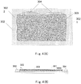
- Fig. 3 , Fig. 4(A)-Fig. 4(B) and Fig. 5(A)-Fig. 5(B) are flow charts of a process for producing the array substrate in the present disclosure.
- the method comprises:
- the peripheral circuit 304 includes an array of scan lines, an array of data lines and other circuits.
- the array of scan lines is produced on the left side and/or right side of the array substrate.
- the array of data lines is produced on the top side and/or bottom side of the array substrate.
- the positions of the array of scan lines and the array of data lines are not limited to the above embodiments. Instead, they may be provided as required in practice.
- Step 203 of cutting the glass substrate 301 that is, cutting the glass substrate 301 along an edge of the first region 3021 formed with the display array 303 to maintain the glass region covered by the first region 3021 while cutting off other parts.
- the part of the glass substrate 301 totally overlapped with the first region 3021 may be maintained while other parts are cut off so as to achieve the production of the display panel with the narrow frame.
- the undesired part of the glass substrate is cut off by a laser cutter or a block wheel mechanism along a cutting position.
- the part of the glass substrate 301 to be cut off may be irradiated by ultraviolet ray such that the attached locations of the glass substrate 301 and the flexible substrate 302 at the irradiated region become gas so as to separate the part of the glass substrate 301 to be cut off from the flexible substrate 302.
- the method further includes: before forming the flexible substrate 302, forming a releasing layer on the glass substrate 301.
- the releasing layer may be produced on the glass substrate 301, and then the flexible substrate 302 is produced on the releasing layer.
- the releasing layer 302 comprises a material which is able to gasify by absorbing laser energy. The material becomes a gas by irradiation of laser such that the flexible substrate is separated from the glass substrate.
- the releasing layer may be formed on an entire surface of the glass substrate 301, or only formed on a surface of the part of the glass substrate to be cut off.
- the releasing layer may be produced by a method such as PVD, CVD, coating. Its material may be selected from one or more of poly(p-xylene), metal oxide, SiNx, SiO 2 , amorphous silicon, III and V Group semiconductor, or hexamethyl disilazane or the combination thereof.
- the method further comprises: after the Step 203, cutting the part in which the peripheral circuit is not produced on the second region 3022 of the flexible substrate 302 to form at least one discontinuous area 3023 on the second region 3022, as illustrated in Fig. 5(A) .
- the discontinuous area 3023 cut out is intended to facilitate the second region 3022 of the flexible substrate 302 to bend to the backside of the display screen when the display panel is produced.
- the corner region on the second region 3022 may be cut to form a discontinuous area which may have arbitrary patterns.
- the discontinuous area is intended to allow the second region 3022 of the flexible substrate 302 to bend conveniently in the subsequent assembling process.
- the corner of the second region 3022 may be cut along the extension lines of two sides of the first region 3021 so as to cut out the discontinuous area as a right angled quadrilateral.
- the method further comprises: after finishing the display array 303 and the peripheral circuit 304, providing the driving chip on the second region of the flexible substrate 302, and providing a part of the flexible circuit board at an edge of the second region of the flexible substrate 302 and electrically connecting the driving chip with the peripheral circuit 304.
- the driving chip includes a scan driving chip and a data driving chip.
- the method further includes: after finishing the display array 303 and the peripheral circuit 304, providing a part of the flexible circuit board at an edge of the second region of the flexible substrate 302, the flexible circuit board being provided with a driving chip thereon, the driving chip being electrically connected with the peripheral circuit 304.
- a layer of flexible substrate is produced on the glass substrate, and a display array and a peripheral circuit are produced on the flexible substrate, and a driving chip, a flexible circuit board are also arranged on the flexible substrate, then the part of the glass substrate below the flexible substrate region on which the peripheral circuit is produced and the driving chip and the flexible circuit board are provided may be cut off.
- the flexible substrate region on which the peripheral circuit is produced and the driving chip and the flexible circuit board are provided may bend to the backside of the display screen, such that the production of a display apparatus with a super narrow frame, even without frame can be achieved.
Landscapes
- Physics & Mathematics (AREA)
- Nonlinear Science (AREA)
- Mathematical Physics (AREA)
- Chemical & Material Sciences (AREA)
- Crystallography & Structural Chemistry (AREA)
- General Physics & Mathematics (AREA)
- Optics & Photonics (AREA)
- Devices For Indicating Variable Information By Combining Individual Elements (AREA)
Claims (11)
- Arraysubstrat, das Folgendes umfasst:ein Glassubstrat (101), das zwei gegenüberliegende Oberflächen aufweist;ein flexibles Substrat (102), das einen ersten Abschnitt (1021) und einen zweiten Abschnitt (1022) umfasst, wobei das Glassubstrat (101) auf einer unteren Oberfläche des ersten Abschnitts (1021) des flexiblen Substrats (102) angeordnet ist, der zweite Abschnitt (1022) ein Abschnitt des flexiblen Substrats (102) anders als der erste Abschnitt (1021) ist und sich an einer Peripherie des ersten Abschnitts (1021) befindet, der zweite Abschnitt (1022) den ersten Abschnitt (1021) umgibt und der zweite Abschnitt (1022) des flexiblen Substrats (102) mit einer Peripherieschaltung (104) darauf versehen ist; undein Anzeigearray (103), das auf dem ersten Abschnitt (1021) des flexiblen Substrats (102) ausgebildet ist,wobei der zweite Abschnitt (1022) des flexiblen Substrats (102) hinsichtlich des Glassubstrats (101) biegbar ist, so dass der zweite Abschnitt (1022) gebogen wird, um ein Ende des Glassubstrats (101) derart zu umhüllen, dass ein Teil des zweiten Abschnitts (1022) mit der Oberfläche des Glassubstrats (101) in Berührung ist, die von dem ersten Abschnitt (1021) entfernt ist.
- Arraysubstrat nach Anspruch 1, wobei der erste Abschnitt (1021) des flexiblen Substrats (102) mit dem Glassubstrat (101) vollständig überlappt ist und der zweite Abschnitt (1022) des flexiblen Substrats (102) sich hinsichtlich des Glassubstrats (101) biegt.
- Arraysubstrat nach Anspruch 1, wobei das Glassubstrat einen Mittelteil des flexiblen Substrats (102) trägt und sich ein Randabschnitt des ersten Abschnitts (1021) und der zweite Abschnitt (1022) des flexiblen Substrats (102) hinsichtlich des Glassubstrats (101) biegen.
- Arraysubstrat nach einem der Ansprüche 1-3, das ferner Folgendes umfasst:
eine Trennschicht, die sich zwischen dem Glassubstrat (101) und dem flexiblen Substrat (102) befindet und ein Material umfasst, das durch Absorbieren von Laserenergie imstande ist, zu vergasen. - Arraysubstrat nach Anspruch 1, wobei das Arraysubstrat ferner mit einer flexiblen Leiterplatte (105), die an einem Rand des zweiten Abschnitts (1022) des flexiblen Substrats (102) teilweise angebracht ist, und einem Treiberchip (106) versehen ist, der an dem zweiten Abschnitt (1022) des flexiblen Substrats (102) angebracht und mit der Peripherieschaltung elektrisch verbunden ist, die mit dem Anzeigearray elektrisch verbunden ist.
- Arraysubstrat nach Anspruch 1, wobei das Arraysubstrat ferner mit einer flexiblen Leiterplatte (105) versehen ist, die an einem Rand des zweiten Abschnitts (1022) des flexiblen Substrats (102) teilweise angebracht ist, wobei die flexible Leiterplatte (105) mit einem Treiberchip (106) darauf versehen ist, wobei der Treiberchip (106) mit der Peripherieschaltung elektrisch verbunden ist, die mit dem Anzeigearray (103) elektrisch verbunden ist.
- Anzeigesubstrat oder Anzeigevorrichtung, das/die das Arraysubstrat nach einem der Ansprüche 1-6 umfasst.
- Verfahren zum Herstellen eines Arraysubstrats, wobei das Verfahren Folgendes umfasst:Ausbilden eines flexiblen Substrats (302) auf einem Glassubstrat (301), wobei das Glassubstrat zwei gegenüberliegende Oberflächen aufweist;Ausbilden eines Anzeigearrays (303) und einer Peripherieschaltung (304) auf dem flexiblen Substrat (302), wobei das flexible Substrat (302) einen ersten Abschnitt (3021), in dem sich das Anzeigearray befindet, und einen zweiten Abschnitt (3022) umfasst, in dem sich die Peripherieschaltung befindet, wobei der zweite Abschnitt (3022) ein Abschnitt des flexiblen Substrats anders als der erste Abschnitt (3021) ist und sich an einer Peripherie des ersten Abschnitts (1021) befindet und der zweite Abschnitt (1022) den ersten Abschnitt (1021) umgibt;Schneiden des Glassubstrats (301) entlang eines Rands des ersten Abschnitts (3021), der mit dem Anzeigearray (303) ausgebildet ist;Trennen des Teils des Glassubstrats (301), der nicht durch den ersten Abschnitt (3021) bedeckt ist, von dem flexiblen Substrat (302);wobei das Verfahren ferner Folgendes umfasst:
Biegen des zweiten Abschnitts (3022) hinsichtlich eines verbleibenden Teils des Glassubstrats, so dass der zweite Abschnitt (3022) ein Ende des verbleibenden Teils des Glassubstrats derart umhüllt, dass ein Teil des zweiten Abschnitts (3022) mit der Oberfläche des verbleibenden Teils des Glassubstrats in Berührung ist, der von dem ersten Abschnitt (3021) entfernt ist. - Verfahren nach Anspruch 8, das ferner Folgendes umfasst:
vor dem Ausbilden des flexiblen Substrats (302), Ausbilden einer Trennschicht auf dem Glassubstrat und Ausbilden des flexiblen Substrats (302) auf der Trennschicht, wobei die Trennschicht ein Material umfasst, das durch Absorbieren von Laserenergie imstande ist, zu vergasen. - Verfahren nach Anspruch 9, wobei die Trennschicht auf einer gesamten Oberfläche des Glassubstrats (301) ausgebildet wird oder nur auf einer Oberfläche des Teils des Glassubstrats (301) ausgebildet wird, der abgeschnitten werden soll.
- Verfahren nach Anspruch 8, wobei der Teil des Glassubstrats (301), der nicht durch den ersten Abschnitt (3021) von dem flexiblen Substrat (302) bedeckt ist, mittels Laserbestrahlung getrennt wird.
Applications Claiming Priority (2)
| Application Number | Priority Date | Filing Date | Title |
|---|---|---|---|
| CN201410217686.XA CN104009044B (zh) | 2014-05-22 | 2014-05-22 | 一种阵列基板及其制作方法、显示基板、显示装置 |
| PCT/CN2014/086676 WO2015176428A1 (zh) | 2014-05-22 | 2014-09-17 | 阵列基板及其制作方法、显示基板、显示装置 |
Publications (3)
| Publication Number | Publication Date |
|---|---|
| EP3147946A1 EP3147946A1 (de) | 2017-03-29 |
| EP3147946A4 EP3147946A4 (de) | 2017-12-13 |
| EP3147946B1 true EP3147946B1 (de) | 2021-04-28 |
Family
ID=51369637
Family Applications (1)
| Application Number | Title | Priority Date | Filing Date |
|---|---|---|---|
| EP14863053.6A Active EP3147946B1 (de) | 2014-05-22 | 2014-09-17 | Arraysubstrat und herstellungsverfahren dafür, anzeigesubstrat und anzeigevorrichtung |
Country Status (4)
| Country | Link |
|---|---|
| US (1) | US9515102B2 (de) |
| EP (1) | EP3147946B1 (de) |
| CN (1) | CN104009044B (de) |
| WO (1) | WO2015176428A1 (de) |
Families Citing this family (48)
| Publication number | Priority date | Publication date | Assignee | Title |
|---|---|---|---|---|
| US10446585B2 (en) * | 2014-03-17 | 2019-10-15 | E Ink Corporation | Multi-layer expanding electrode structures for backplane assemblies |
| CN104009044B (zh) | 2014-05-22 | 2018-11-23 | 京东方科技集团股份有限公司 | 一种阵列基板及其制作方法、显示基板、显示装置 |
| TWI587768B (zh) * | 2014-09-12 | 2017-06-11 | 友達光電股份有限公司 | 顯示裝置 |
| CN104317080A (zh) * | 2014-10-31 | 2015-01-28 | 京东方科技集团股份有限公司 | 一种显示装置及其制作方法 |
| CN104409476A (zh) * | 2014-12-11 | 2015-03-11 | 昆山国显光电有限公司 | 显示模组 |
| US10395615B2 (en) | 2014-12-25 | 2019-08-27 | Shanghai Tianma Micro-electronics Co., Ltd. | Display panel and method for manufacturing the same cross-references to related applications |
| CN108535907B (zh) * | 2014-12-25 | 2021-07-20 | 上海天马微电子有限公司 | 一种显示面板、显示器及其制作方法 |
| KR102386891B1 (ko) * | 2015-03-11 | 2022-04-15 | 삼성디스플레이 주식회사 | 표시 장치 및 이를 제조하는 방법 |
| KR20160110861A (ko) | 2015-03-13 | 2016-09-22 | 삼성디스플레이 주식회사 | 연성 회로 기판 및 이를 포함하는 표시 장치 |
| CN204884440U (zh) * | 2015-08-27 | 2015-12-16 | 京东方科技集团股份有限公司 | 柔性显示面板和柔性显示装置 |
| CN105223747B (zh) * | 2015-10-27 | 2019-04-05 | 南京中电熊猫液晶显示科技有限公司 | 一种显示面板 |
| CN106887187A (zh) | 2015-12-16 | 2017-06-23 | 昆山工研院新型平板显示技术中心有限公司 | 一种无边框显示装置及其制备方法 |
| CN106066550A (zh) * | 2016-07-28 | 2016-11-02 | 武汉华星光电技术有限公司 | 液晶显示器、液晶显示面板及其制备方法 |
| KR102721751B1 (ko) * | 2016-12-16 | 2024-10-23 | 엘지디스플레이 주식회사 | 플렉서블 표시 장치 |
| TWI598661B (zh) * | 2016-12-26 | 2017-09-11 | 友達光電股份有限公司 | 顯示裝置 |
| CN106790811B (zh) * | 2016-12-26 | 2019-11-26 | 武汉华星光电技术有限公司 | 显示屏驱动系统及移动终端 |
| WO2018120139A1 (zh) * | 2016-12-30 | 2018-07-05 | 深圳市柔宇科技有限公司 | 柔性显示屏和显示装置 |
| KR20190032596A (ko) * | 2016-12-30 | 2019-03-27 | 선전 로욜 테크놀로지스 컴퍼니 리미티드 | 디스플레이 패널 |
| CN107742628A (zh) * | 2017-09-12 | 2018-02-27 | 奕瑞影像科技(太仓)有限公司 | 柔性闪烁屏、放射线图像传感器及其制备方法 |
| CN109712528A (zh) * | 2017-10-25 | 2019-05-03 | 北京小米移动软件有限公司 | 屏幕模组及电子设备 |
| CN107931845B (zh) * | 2017-11-20 | 2020-05-05 | 武汉华星光电半导体显示技术有限公司 | 切割方法 |
| CN107863055B (zh) * | 2017-11-29 | 2021-06-22 | 武汉天马微电子有限公司 | 一种柔性基板及其状态检测方法、显示装置 |
| CN108051965A (zh) * | 2018-01-02 | 2018-05-18 | 京东方(河北)移动显示技术有限公司 | 显示基板及制造方法、显示装置及制造方法、移动终端 |
| CN110021234B (zh) * | 2018-01-08 | 2022-03-08 | 上海和辉光电股份有限公司 | 一种阵列基板及其制作方法、柔性显示面板 |
| CN108336113B (zh) * | 2018-01-31 | 2021-01-26 | 武汉华星光电半导体显示技术有限公司 | 减弱激光灼伤的cof及柔性显示装置 |
| CN108364986B (zh) * | 2018-02-09 | 2020-12-22 | 京东方科技集团股份有限公司 | 显示基板和显示装置 |
| CN110308579B (zh) * | 2018-03-22 | 2022-04-12 | 上海和辉光电股份有限公司 | 一种刚性显示面板及其制作方法 |
| CN108648710A (zh) * | 2018-05-11 | 2018-10-12 | 昆山国显光电有限公司 | 阵列基板、显示面板、显示装置及阵列基板的制备方法 |
| CN108693999B (zh) * | 2018-05-14 | 2021-06-29 | 昆山国显光电有限公司 | 异形显示装置及其制备方法 |
| CN110515481B (zh) * | 2018-05-22 | 2023-05-26 | 鸿富锦精密工业(深圳)有限公司 | 电子装置及电子装置的制造方法 |
| CN108682369A (zh) * | 2018-05-22 | 2018-10-19 | Oppo广东移动通信有限公司 | 一种显示面板及全面屏显示装置 |
| CN108803103A (zh) * | 2018-05-30 | 2018-11-13 | 上海中航光电子有限公司 | 一种液晶显示装置及其制作方法 |
| CN113419370B (zh) * | 2018-06-06 | 2022-10-18 | 上海中航光电子有限公司 | 液晶显示装置 |
| CN109188801A (zh) * | 2018-09-26 | 2019-01-11 | 武汉天马微电子有限公司 | 一种显示面板及其制备方法 |
| CN109523949A (zh) * | 2018-11-15 | 2019-03-26 | 武汉华星光电半导体显示技术有限公司 | 显示面板 |
| CN111200063A (zh) * | 2018-11-20 | 2020-05-26 | 陕西坤同半导体科技有限公司 | 载板玻璃以及用于制备柔性基板的层叠结构 |
| CN109493745B (zh) * | 2018-11-28 | 2020-06-16 | 武汉华星光电技术有限公司 | 显示装置及其制作方法 |
| CN111240109A (zh) * | 2018-11-29 | 2020-06-05 | 北京小米移动软件有限公司 | 显示面板及其制备方法、显示装置 |
| CN109459896A (zh) * | 2018-12-29 | 2019-03-12 | 武汉华星光电技术有限公司 | 窄边框显示模块及其显示装置 |
| CN109980123A (zh) * | 2019-03-19 | 2019-07-05 | 武汉华星光电半导体显示技术有限公司 | 刚性oled显示面板的制备方法及显示面板 |
| CN110310577B (zh) * | 2019-07-05 | 2021-01-01 | 武汉华星光电半导体显示技术有限公司 | 显示面板及其制备方法 |
| CN110426877B (zh) * | 2019-07-08 | 2020-10-27 | 深圳市华星光电技术有限公司 | 一种窄边框显示面板及其制备方法、窄边框显示装置 |
| CN110853572A (zh) | 2019-11-27 | 2020-02-28 | 深圳市华星光电半导体显示技术有限公司 | 显示面板和显示装置 |
| CN114078364A (zh) * | 2020-08-17 | 2022-02-22 | 深圳市柔宇科技股份有限公司 | 显示面板、显示装置 |
| CN112701085A (zh) * | 2020-12-28 | 2021-04-23 | 广东聚华印刷显示技术有限公司 | 柔性显示器的制造方法及柔性显示器 |
| CN113534516A (zh) * | 2021-06-16 | 2021-10-22 | 北海惠科光电技术有限公司 | 阵列基板、显示装置及显示装置的制作方法 |
| CN114822298B (zh) * | 2022-06-27 | 2022-09-30 | 季华实验室 | 一种基于玻璃基板的显示单元的制造方法及显示单元 |
| CN119596586A (zh) * | 2024-11-29 | 2025-03-11 | 惠科股份有限公司 | 显示模组 |
Citations (4)
| Publication number | Priority date | Publication date | Assignee | Title |
|---|---|---|---|---|
| US20110059561A1 (en) * | 2009-09-08 | 2011-03-10 | Chimei Innolux Corporation | Method for fabricating a flexible display device |
| US20110147747A1 (en) * | 2009-12-21 | 2011-06-23 | Jeon Hyung-Il | Display Device and Method of Manufacturing the Same |
| US20130335660A1 (en) * | 2012-06-18 | 2013-12-19 | Samsung Display Co., Ltd. | Display panel and method of manufacturing the same |
| US20140104528A1 (en) * | 2012-10-17 | 2014-04-17 | Samsung Display Co., Ltd. | Display panel and method of manufacturing the same |
Family Cites Families (16)
| Publication number | Priority date | Publication date | Assignee | Title |
|---|---|---|---|---|
| US4764413A (en) | 1984-09-13 | 1988-08-16 | Sharp Kabushiki Kaisha | Metal-based organic film substrate |
| JP4445189B2 (ja) * | 2002-08-29 | 2010-04-07 | 株式会社ルネサステクノロジ | 半導体装置およびその製造方法 |
| JP4004994B2 (ja) * | 2003-06-05 | 2007-11-07 | 株式会社アドバンスト・ディスプレイ | 表示装置 |
| TWI373081B (en) * | 2008-09-09 | 2012-09-21 | Prime View Int Co Ltd | Flexible display panel |
| CN101996535A (zh) * | 2009-08-25 | 2011-03-30 | 精工爱普生株式会社 | 电光学装置和电子设备 |
| US8724038B2 (en) * | 2010-10-18 | 2014-05-13 | Qualcomm Mems Technologies, Inc. | Wraparound assembly for combination touch, handwriting and fingerprint sensor |
| JP5720222B2 (ja) * | 2010-12-13 | 2015-05-20 | ソニー株式会社 | 表示装置及び電子機器 |
| US8716932B2 (en) * | 2011-02-28 | 2014-05-06 | Apple Inc. | Displays with minimized borders |
| TWI449007B (zh) * | 2011-09-16 | 2014-08-11 | E Ink Holdings Inc | 可撓性顯示裝置的製造方法 |
| CN102636898B (zh) * | 2012-03-14 | 2014-03-12 | 京东方科技集团股份有限公司 | 一种柔性显示装置的制备方法 |
| US9419065B2 (en) * | 2012-08-07 | 2016-08-16 | Apple Inc. | Flexible displays |
| US9214507B2 (en) * | 2012-08-17 | 2015-12-15 | Apple Inc. | Narrow border organic light-emitting diode display |
| JP6033880B2 (ja) * | 2012-11-12 | 2016-11-30 | シャープ株式会社 | 表示装置 |
| TWM455211U (zh) | 2013-02-05 | 2013-06-11 | Unidisplay Inc | 觸控面板以及觸控顯示面板 |
| CN103558703B (zh) * | 2013-10-12 | 2016-08-10 | 深圳市华星光电技术有限公司 | 超窄边框液晶显示器及其驱动电路的cof封装结构 |
| CN104009044B (zh) | 2014-05-22 | 2018-11-23 | 京东方科技集团股份有限公司 | 一种阵列基板及其制作方法、显示基板、显示装置 |
-
2014
- 2014-05-22 CN CN201410217686.XA patent/CN104009044B/zh active Active
- 2014-09-17 EP EP14863053.6A patent/EP3147946B1/de active Active
- 2014-09-17 US US14/646,866 patent/US9515102B2/en active Active
- 2014-09-17 WO PCT/CN2014/086676 patent/WO2015176428A1/zh not_active Ceased
Patent Citations (4)
| Publication number | Priority date | Publication date | Assignee | Title |
|---|---|---|---|---|
| US20110059561A1 (en) * | 2009-09-08 | 2011-03-10 | Chimei Innolux Corporation | Method for fabricating a flexible display device |
| US20110147747A1 (en) * | 2009-12-21 | 2011-06-23 | Jeon Hyung-Il | Display Device and Method of Manufacturing the Same |
| US20130335660A1 (en) * | 2012-06-18 | 2013-12-19 | Samsung Display Co., Ltd. | Display panel and method of manufacturing the same |
| US20140104528A1 (en) * | 2012-10-17 | 2014-04-17 | Samsung Display Co., Ltd. | Display panel and method of manufacturing the same |
Also Published As
| Publication number | Publication date |
|---|---|
| US20160268318A1 (en) | 2016-09-15 |
| WO2015176428A1 (zh) | 2015-11-26 |
| US9515102B2 (en) | 2016-12-06 |
| CN104009044A (zh) | 2014-08-27 |
| EP3147946A1 (de) | 2017-03-29 |
| EP3147946A4 (de) | 2017-12-13 |
| CN104009044B (zh) | 2018-11-23 |
Similar Documents
| Publication | Publication Date | Title |
|---|---|---|
| EP3147946B1 (de) | Arraysubstrat und herstellungsverfahren dafür, anzeigesubstrat und anzeigevorrichtung | |
| US10714562B2 (en) | Display panel and display device | |
| CN107195642B (zh) | 柔性显示面板及其制备方法、显示装置 | |
| CN104868058B (zh) | 一种显示面板、显示装置和显示面板母板 | |
| US7968882B2 (en) | Flexible display device and manufacturing method thereof | |
| TWI587768B (zh) | 顯示裝置 | |
| JP6945994B2 (ja) | 表示装置 | |
| US10923453B2 (en) | Bonding apparatus and method for using the same | |
| US20150255527A1 (en) | Manufacturing method of display device, display device, and display device formation substrate | |
| CN115050792A (zh) | 柔性显示装置 | |
| US11380628B2 (en) | Mother substrate for display substrates, manufacture method thereof, display substrate and display device | |
| WO2012147672A1 (ja) | 表示モジュール及び表示装置 | |
| US20200091225A1 (en) | Micro led display panel and manufacturing method thereof | |
| TWI565380B (zh) | 顯示裝置及其製造方法 | |
| CN106796364A (zh) | 包括具有增强部分的配线的柔性显示装置及其制造方法 | |
| JP2010072380A (ja) | 表示装置 | |
| KR102552270B1 (ko) | 원장보호필름의 박리방법 및 유기발광 표시장치의 제조방법 | |
| US11815955B2 (en) | Display device, flexible wiring board, and manufacturing method of display device | |
| TW201605567A (zh) | 顯示模組的製造方法及顯示模組 | |
| KR102126537B1 (ko) | 게이트 인 패널 구조의 박막 트랜지스터 어레이 기판 | |
| US11296177B2 (en) | Display device with curable pattern between lead wirings and method of fabricating the same | |
| WO2022226884A1 (zh) | 显示面板 | |
| US20220037298A1 (en) | Display module, preparation method thereof, and electronic device | |
| CN115224217A (zh) | 一种显示模组及制备方法 | |
| US10446586B2 (en) | Pixel unit, array substrate and manufacturing method therefor, display panel and display device |
Legal Events
| Date | Code | Title | Description |
|---|---|---|---|
| PUAI | Public reference made under article 153(3) epc to a published international application that has entered the european phase |
Free format text: ORIGINAL CODE: 0009012 |
|
| STAA | Information on the status of an ep patent application or granted ep patent |
Free format text: STATUS: REQUEST FOR EXAMINATION WAS MADE |
|
| 17P | Request for examination filed |
Effective date: 20150526 |
|
| AK | Designated contracting states |
Kind code of ref document: A1 Designated state(s): AL AT BE BG CH CY CZ DE DK EE ES FI FR GB GR HR HU IE IS IT LI LT LU LV MC MK MT NL NO PL PT RO RS SE SI SK SM TR |
|
| AX | Request for extension of the european patent |
Extension state: BA ME |
|
| DAX | Request for extension of the european patent (deleted) | ||
| A4 | Supplementary search report drawn up and despatched |
Effective date: 20171113 |
|
| RIC1 | Information provided on ipc code assigned before grant |
Ipc: G02F 1/1345 20060101AFI20171107BHEP Ipc: G02F 1/1362 20060101ALN20171107BHEP Ipc: H01L 27/12 20060101ALI20171107BHEP Ipc: H05K 1/18 20060101ALI20171107BHEP Ipc: H05K 1/02 20060101ALI20171107BHEP Ipc: G02F 1/1333 20060101ALN20171107BHEP Ipc: H01L 51/00 20060101ALI20171107BHEP |
|
| STAA | Information on the status of an ep patent application or granted ep patent |
Free format text: STATUS: EXAMINATION IS IN PROGRESS |
|
| 17Q | First examination report despatched |
Effective date: 20200420 |
|
| REG | Reference to a national code |
Ref country code: DE Ref legal event code: R079 Ref document number: 602014077063 Country of ref document: DE Free format text: PREVIOUS MAIN CLASS: H01L0027120000 Ipc: G02F0001134500 |
|
| GRAP | Despatch of communication of intention to grant a patent |
Free format text: ORIGINAL CODE: EPIDOSNIGR1 |
|
| STAA | Information on the status of an ep patent application or granted ep patent |
Free format text: STATUS: GRANT OF PATENT IS INTENDED |
|
| RIC1 | Information provided on ipc code assigned before grant |
Ipc: H05K 1/18 20060101ALI20201030BHEP Ipc: G02F 1/1362 20060101ALN20201030BHEP Ipc: G02F 1/1333 20060101ALN20201030BHEP Ipc: H01L 27/12 20060101ALI20201030BHEP Ipc: H01L 51/00 20060101ALI20201030BHEP Ipc: H05K 1/02 20060101ALI20201030BHEP Ipc: G02F 1/1345 20060101AFI20201030BHEP |
|
| INTG | Intention to grant announced |
Effective date: 20201120 |
|
| RIC1 | Information provided on ipc code assigned before grant |
Ipc: G02F 1/1362 20060101ALN20201110BHEP Ipc: H05K 1/02 20060101ALI20201110BHEP Ipc: H05K 1/18 20060101ALI20201110BHEP Ipc: G02F 1/1345 20060101AFI20201110BHEP Ipc: G02F 1/1333 20060101ALN20201110BHEP Ipc: H01L 27/12 20060101ALI20201110BHEP Ipc: H01L 51/00 20060101ALI20201110BHEP |
|
| GRAS | Grant fee paid |
Free format text: ORIGINAL CODE: EPIDOSNIGR3 |
|
| GRAA | (expected) grant |
Free format text: ORIGINAL CODE: 0009210 |
|
| STAA | Information on the status of an ep patent application or granted ep patent |
Free format text: STATUS: THE PATENT HAS BEEN GRANTED |
|
| AK | Designated contracting states |
Kind code of ref document: B1 Designated state(s): AL AT BE BG CH CY CZ DE DK EE ES FI FR GB GR HR HU IE IS IT LI LT LU LV MC MK MT NL NO PL PT RO RS SE SI SK SM TR |
|
| REG | Reference to a national code |
Ref country code: GB Ref legal event code: FG4D |
|
| REG | Reference to a national code |
Ref country code: CH Ref legal event code: EP |
|
| REG | Reference to a national code |
Ref country code: AT Ref legal event code: REF Ref document number: 1387751 Country of ref document: AT Kind code of ref document: T Effective date: 20210515 |
|
| REG | Reference to a national code |
Ref country code: DE Ref legal event code: R096 Ref document number: 602014077063 Country of ref document: DE |
|
| REG | Reference to a national code |
Ref country code: IE Ref legal event code: FG4D |
|
| REG | Reference to a national code |
Ref country code: LT Ref legal event code: MG9D |
|
| REG | Reference to a national code |
Ref country code: AT Ref legal event code: MK05 Ref document number: 1387751 Country of ref document: AT Kind code of ref document: T Effective date: 20210428 |
|
| PG25 | Lapsed in a contracting state [announced via postgrant information from national office to epo] |
Ref country code: LT Free format text: LAPSE BECAUSE OF FAILURE TO SUBMIT A TRANSLATION OF THE DESCRIPTION OR TO PAY THE FEE WITHIN THE PRESCRIBED TIME-LIMIT Effective date: 20210428 Ref country code: NL Free format text: LAPSE BECAUSE OF FAILURE TO SUBMIT A TRANSLATION OF THE DESCRIPTION OR TO PAY THE FEE WITHIN THE PRESCRIBED TIME-LIMIT Effective date: 20210428 Ref country code: FI Free format text: LAPSE BECAUSE OF FAILURE TO SUBMIT A TRANSLATION OF THE DESCRIPTION OR TO PAY THE FEE WITHIN THE PRESCRIBED TIME-LIMIT Effective date: 20210428 Ref country code: AT Free format text: LAPSE BECAUSE OF FAILURE TO SUBMIT A TRANSLATION OF THE DESCRIPTION OR TO PAY THE FEE WITHIN THE PRESCRIBED TIME-LIMIT Effective date: 20210428 Ref country code: BG Free format text: LAPSE BECAUSE OF FAILURE TO SUBMIT A TRANSLATION OF THE DESCRIPTION OR TO PAY THE FEE WITHIN THE PRESCRIBED TIME-LIMIT Effective date: 20210728 Ref country code: HR Free format text: LAPSE BECAUSE OF FAILURE TO SUBMIT A TRANSLATION OF THE DESCRIPTION OR TO PAY THE FEE WITHIN THE PRESCRIBED TIME-LIMIT Effective date: 20210428 |
|
| PG25 | Lapsed in a contracting state [announced via postgrant information from national office to epo] |
Ref country code: RS Free format text: LAPSE BECAUSE OF FAILURE TO SUBMIT A TRANSLATION OF THE DESCRIPTION OR TO PAY THE FEE WITHIN THE PRESCRIBED TIME-LIMIT Effective date: 20210428 Ref country code: SE Free format text: LAPSE BECAUSE OF FAILURE TO SUBMIT A TRANSLATION OF THE DESCRIPTION OR TO PAY THE FEE WITHIN THE PRESCRIBED TIME-LIMIT Effective date: 20210428 Ref country code: ES Free format text: LAPSE BECAUSE OF FAILURE TO SUBMIT A TRANSLATION OF THE DESCRIPTION OR TO PAY THE FEE WITHIN THE PRESCRIBED TIME-LIMIT Effective date: 20210428 Ref country code: PT Free format text: LAPSE BECAUSE OF FAILURE TO SUBMIT A TRANSLATION OF THE DESCRIPTION OR TO PAY THE FEE WITHIN THE PRESCRIBED TIME-LIMIT Effective date: 20210830 Ref country code: PL Free format text: LAPSE BECAUSE OF FAILURE TO SUBMIT A TRANSLATION OF THE DESCRIPTION OR TO PAY THE FEE WITHIN THE PRESCRIBED TIME-LIMIT Effective date: 20210428 Ref country code: NO Free format text: LAPSE BECAUSE OF FAILURE TO SUBMIT A TRANSLATION OF THE DESCRIPTION OR TO PAY THE FEE WITHIN THE PRESCRIBED TIME-LIMIT Effective date: 20210728 Ref country code: GR Free format text: LAPSE BECAUSE OF FAILURE TO SUBMIT A TRANSLATION OF THE DESCRIPTION OR TO PAY THE FEE WITHIN THE PRESCRIBED TIME-LIMIT Effective date: 20210729 Ref country code: LV Free format text: LAPSE BECAUSE OF FAILURE TO SUBMIT A TRANSLATION OF THE DESCRIPTION OR TO PAY THE FEE WITHIN THE PRESCRIBED TIME-LIMIT Effective date: 20210428 Ref country code: IS Free format text: LAPSE BECAUSE OF FAILURE TO SUBMIT A TRANSLATION OF THE DESCRIPTION OR TO PAY THE FEE WITHIN THE PRESCRIBED TIME-LIMIT Effective date: 20210828 |
|
| REG | Reference to a national code |
Ref country code: NL Ref legal event code: MP Effective date: 20210428 |
|
| PG25 | Lapsed in a contracting state [announced via postgrant information from national office to epo] |
Ref country code: SK Free format text: LAPSE BECAUSE OF FAILURE TO SUBMIT A TRANSLATION OF THE DESCRIPTION OR TO PAY THE FEE WITHIN THE PRESCRIBED TIME-LIMIT Effective date: 20210428 Ref country code: SM Free format text: LAPSE BECAUSE OF FAILURE TO SUBMIT A TRANSLATION OF THE DESCRIPTION OR TO PAY THE FEE WITHIN THE PRESCRIBED TIME-LIMIT Effective date: 20210428 Ref country code: EE Free format text: LAPSE BECAUSE OF FAILURE TO SUBMIT A TRANSLATION OF THE DESCRIPTION OR TO PAY THE FEE WITHIN THE PRESCRIBED TIME-LIMIT Effective date: 20210428 Ref country code: DK Free format text: LAPSE BECAUSE OF FAILURE TO SUBMIT A TRANSLATION OF THE DESCRIPTION OR TO PAY THE FEE WITHIN THE PRESCRIBED TIME-LIMIT Effective date: 20210428 Ref country code: CZ Free format text: LAPSE BECAUSE OF FAILURE TO SUBMIT A TRANSLATION OF THE DESCRIPTION OR TO PAY THE FEE WITHIN THE PRESCRIBED TIME-LIMIT Effective date: 20210428 Ref country code: RO Free format text: LAPSE BECAUSE OF FAILURE TO SUBMIT A TRANSLATION OF THE DESCRIPTION OR TO PAY THE FEE WITHIN THE PRESCRIBED TIME-LIMIT Effective date: 20210428 |
|
| REG | Reference to a national code |
Ref country code: DE Ref legal event code: R097 Ref document number: 602014077063 Country of ref document: DE |
|
| PLBE | No opposition filed within time limit |
Free format text: ORIGINAL CODE: 0009261 |
|
| STAA | Information on the status of an ep patent application or granted ep patent |
Free format text: STATUS: NO OPPOSITION FILED WITHIN TIME LIMIT |
|
| 26N | No opposition filed |
Effective date: 20220131 |
|
| REG | Reference to a national code |
Ref country code: CH Ref legal event code: PL |
|
| REG | Reference to a national code |
Ref country code: BE Ref legal event code: MM Effective date: 20210930 |
|
| GBPC | Gb: european patent ceased through non-payment of renewal fee |
Effective date: 20210917 |
|
| PG25 | Lapsed in a contracting state [announced via postgrant information from national office to epo] |
Ref country code: IS Free format text: LAPSE BECAUSE OF FAILURE TO SUBMIT A TRANSLATION OF THE DESCRIPTION OR TO PAY THE FEE WITHIN THE PRESCRIBED TIME-LIMIT Effective date: 20210828 Ref country code: MC Free format text: LAPSE BECAUSE OF FAILURE TO SUBMIT A TRANSLATION OF THE DESCRIPTION OR TO PAY THE FEE WITHIN THE PRESCRIBED TIME-LIMIT Effective date: 20210428 Ref country code: AL Free format text: LAPSE BECAUSE OF FAILURE TO SUBMIT A TRANSLATION OF THE DESCRIPTION OR TO PAY THE FEE WITHIN THE PRESCRIBED TIME-LIMIT Effective date: 20210428 |
|
| PG25 | Lapsed in a contracting state [announced via postgrant information from national office to epo] |
Ref country code: LU Free format text: LAPSE BECAUSE OF NON-PAYMENT OF DUE FEES Effective date: 20210917 Ref country code: IT Free format text: LAPSE BECAUSE OF FAILURE TO SUBMIT A TRANSLATION OF THE DESCRIPTION OR TO PAY THE FEE WITHIN THE PRESCRIBED TIME-LIMIT Effective date: 20210428 Ref country code: IE Free format text: LAPSE BECAUSE OF NON-PAYMENT OF DUE FEES Effective date: 20210917 Ref country code: GB Free format text: LAPSE BECAUSE OF NON-PAYMENT OF DUE FEES Effective date: 20210917 Ref country code: FR Free format text: LAPSE BECAUSE OF NON-PAYMENT OF DUE FEES Effective date: 20210930 Ref country code: BE Free format text: LAPSE BECAUSE OF NON-PAYMENT OF DUE FEES Effective date: 20210930 |
|
| PG25 | Lapsed in a contracting state [announced via postgrant information from national office to epo] |
Ref country code: LI Free format text: LAPSE BECAUSE OF NON-PAYMENT OF DUE FEES Effective date: 20210930 Ref country code: CH Free format text: LAPSE BECAUSE OF NON-PAYMENT OF DUE FEES Effective date: 20210930 |
|
| PG25 | Lapsed in a contracting state [announced via postgrant information from national office to epo] |
Ref country code: HU Free format text: LAPSE BECAUSE OF FAILURE TO SUBMIT A TRANSLATION OF THE DESCRIPTION OR TO PAY THE FEE WITHIN THE PRESCRIBED TIME-LIMIT; INVALID AB INITIO Effective date: 20140917 |
|
| PG25 | Lapsed in a contracting state [announced via postgrant information from national office to epo] |
Ref country code: CY Free format text: LAPSE BECAUSE OF FAILURE TO SUBMIT A TRANSLATION OF THE DESCRIPTION OR TO PAY THE FEE WITHIN THE PRESCRIBED TIME-LIMIT Effective date: 20210428 |
|
| PG25 | Lapsed in a contracting state [announced via postgrant information from national office to epo] |
Ref country code: MK Free format text: LAPSE BECAUSE OF FAILURE TO SUBMIT A TRANSLATION OF THE DESCRIPTION OR TO PAY THE FEE WITHIN THE PRESCRIBED TIME-LIMIT Effective date: 20210428 |
|
| PG25 | Lapsed in a contracting state [announced via postgrant information from national office to epo] |
Ref country code: TR Free format text: LAPSE BECAUSE OF FAILURE TO SUBMIT A TRANSLATION OF THE DESCRIPTION OR TO PAY THE FEE WITHIN THE PRESCRIBED TIME-LIMIT Effective date: 20210428 |
|
| PG25 | Lapsed in a contracting state [announced via postgrant information from national office to epo] |
Ref country code: MT Free format text: LAPSE BECAUSE OF FAILURE TO SUBMIT A TRANSLATION OF THE DESCRIPTION OR TO PAY THE FEE WITHIN THE PRESCRIBED TIME-LIMIT Effective date: 20210428 |
|
| PGFP | Annual fee paid to national office [announced via postgrant information from national office to epo] |
Ref country code: DE Payment date: 20240919 Year of fee payment: 11 |