EP3147953A1 - Module de cellule solaire - Google Patents
Module de cellule solaire Download PDFInfo
- Publication number
- EP3147953A1 EP3147953A1 EP16190777.9A EP16190777A EP3147953A1 EP 3147953 A1 EP3147953 A1 EP 3147953A1 EP 16190777 A EP16190777 A EP 16190777A EP 3147953 A1 EP3147953 A1 EP 3147953A1
- Authority
- EP
- European Patent Office
- Prior art keywords
- solar cell
- wiring members
- finger electrodes
- metal foils
- cell module
- Prior art date
- Legal status (The legal status is an assumption and is not a legal conclusion. Google has not performed a legal analysis and makes no representation as to the accuracy of the status listed.)
- Withdrawn
Links
- 229910052751 metal Inorganic materials 0.000 claims abstract description 137
- 239000002184 metal Substances 0.000 claims abstract description 137
- 239000011888 foil Substances 0.000 claims abstract description 131
- 238000006243 chemical reaction Methods 0.000 claims abstract description 43
- 239000000853 adhesive Substances 0.000 description 35
- 230000001070 adhesive effect Effects 0.000 description 35
- 239000010410 layer Substances 0.000 description 21
- 239000002245 particle Substances 0.000 description 13
- 239000003566 sealing material Substances 0.000 description 13
- 229920005989 resin Polymers 0.000 description 11
- 239000011347 resin Substances 0.000 description 11
- 238000010586 diagram Methods 0.000 description 8
- 239000000758 substrate Substances 0.000 description 8
- 239000004065 semiconductor Substances 0.000 description 7
- BQCADISMDOOEFD-UHFFFAOYSA-N Silver Chemical compound [Ag] BQCADISMDOOEFD-UHFFFAOYSA-N 0.000 description 5
- 239000000969 carrier Substances 0.000 description 5
- 229910021419 crystalline silicon Inorganic materials 0.000 description 5
- 229910052709 silver Inorganic materials 0.000 description 5
- 239000004332 silver Substances 0.000 description 5
- PXHVJJICTQNCMI-UHFFFAOYSA-N Nickel Chemical compound [Ni] PXHVJJICTQNCMI-UHFFFAOYSA-N 0.000 description 4
- 229910021417 amorphous silicon Inorganic materials 0.000 description 4
- 230000015572 biosynthetic process Effects 0.000 description 4
- 239000000470 constituent Substances 0.000 description 4
- 230000000694 effects Effects 0.000 description 4
- 239000005038 ethylene vinyl acetate Substances 0.000 description 4
- 239000000463 material Substances 0.000 description 4
- 229920001200 poly(ethylene-vinyl acetate) Polymers 0.000 description 4
- 239000010409 thin film Substances 0.000 description 4
- 235000012431 wafers Nutrition 0.000 description 4
- RYGMFSIKBFXOCR-UHFFFAOYSA-N Copper Chemical compound [Cu] RYGMFSIKBFXOCR-UHFFFAOYSA-N 0.000 description 3
- 229910052782 aluminium Inorganic materials 0.000 description 3
- XAGFODPZIPBFFR-UHFFFAOYSA-N aluminium Chemical compound [Al] XAGFODPZIPBFFR-UHFFFAOYSA-N 0.000 description 3
- 229910052802 copper Inorganic materials 0.000 description 3
- 239000010949 copper Substances 0.000 description 3
- 239000011521 glass Substances 0.000 description 3
- 150000002739 metals Chemical class 0.000 description 3
- 229910045601 alloy Inorganic materials 0.000 description 2
- 239000000956 alloy Substances 0.000 description 2
- 239000011230 binding agent Substances 0.000 description 2
- 150000001735 carboxylic acids Chemical class 0.000 description 2
- 229920001577 copolymer Polymers 0.000 description 2
- 239000010408 film Substances 0.000 description 2
- 229910003437 indium oxide Inorganic materials 0.000 description 2
- PJXISJQVUVHSOJ-UHFFFAOYSA-N indium(iii) oxide Chemical compound [O-2].[O-2].[O-2].[In+3].[In+3] PJXISJQVUVHSOJ-UHFFFAOYSA-N 0.000 description 2
- 238000010030 laminating Methods 0.000 description 2
- 239000007788 liquid Substances 0.000 description 2
- 238000004519 manufacturing process Methods 0.000 description 2
- 238000000034 method Methods 0.000 description 2
- 229910052759 nickel Inorganic materials 0.000 description 2
- 229920005672 polyolefin resin Polymers 0.000 description 2
- 238000010248 power generation Methods 0.000 description 2
- 238000009751 slip forming Methods 0.000 description 2
- 239000004711 α-olefin Substances 0.000 description 2
- KXGFMDJXCMQABM-UHFFFAOYSA-N 2-methoxy-6-methylphenol Chemical compound [CH]OC1=CC=CC([CH])=C1O KXGFMDJXCMQABM-UHFFFAOYSA-N 0.000 description 1
- 239000004925 Acrylic resin Substances 0.000 description 1
- 229920000178 Acrylic resin Polymers 0.000 description 1
- 229910000838 Al alloy Inorganic materials 0.000 description 1
- JBRZTFJDHDCESZ-UHFFFAOYSA-N AsGa Chemical compound [As]#[Ga] JBRZTFJDHDCESZ-UHFFFAOYSA-N 0.000 description 1
- OKTJSMMVPCPJKN-UHFFFAOYSA-N Carbon Chemical compound [C] OKTJSMMVPCPJKN-UHFFFAOYSA-N 0.000 description 1
- GPXJNWSHGFTCBW-UHFFFAOYSA-N Indium phosphide Chemical compound [In]#P GPXJNWSHGFTCBW-UHFFFAOYSA-N 0.000 description 1
- ATJFFYVFTNAWJD-UHFFFAOYSA-N Tin Chemical compound [Sn] ATJFFYVFTNAWJD-UHFFFAOYSA-N 0.000 description 1
- GWEVSGVZZGPLCZ-UHFFFAOYSA-N Titan oxide Chemical compound O=[Ti]=O GWEVSGVZZGPLCZ-UHFFFAOYSA-N 0.000 description 1
- 229920001807 Urea-formaldehyde Polymers 0.000 description 1
- XLOMVQKBTHCTTD-UHFFFAOYSA-N Zinc monoxide Chemical compound [Zn]=O XLOMVQKBTHCTTD-UHFFFAOYSA-N 0.000 description 1
- 239000012790 adhesive layer Substances 0.000 description 1
- 229910052787 antimony Inorganic materials 0.000 description 1
- WATWJIUSRGPENY-UHFFFAOYSA-N antimony atom Chemical compound [Sb] WATWJIUSRGPENY-UHFFFAOYSA-N 0.000 description 1
- 229910052799 carbon Inorganic materials 0.000 description 1
- 230000015556 catabolic process Effects 0.000 description 1
- 230000007423 decrease Effects 0.000 description 1
- 230000003247 decreasing effect Effects 0.000 description 1
- 238000006731 degradation reaction Methods 0.000 description 1
- 239000003822 epoxy resin Substances 0.000 description 1
- 150000003949 imides Chemical class 0.000 description 1
- 230000001771 impaired effect Effects 0.000 description 1
- 238000003475 lamination Methods 0.000 description 1
- 229910044991 metal oxide Inorganic materials 0.000 description 1
- 150000004706 metal oxides Chemical class 0.000 description 1
- 239000002923 metal particle Substances 0.000 description 1
- 239000000203 mixture Substances 0.000 description 1
- 229920001568 phenolic resin Polymers 0.000 description 1
- 239000005011 phenolic resin Substances 0.000 description 1
- 238000007747 plating Methods 0.000 description 1
- 229920000647 polyepoxide Polymers 0.000 description 1
- 230000002265 prevention Effects 0.000 description 1
- 229910000679 solder Inorganic materials 0.000 description 1
- 230000001629 suppression Effects 0.000 description 1
- 229920002803 thermoplastic polyurethane Polymers 0.000 description 1
- 229920001187 thermosetting polymer Polymers 0.000 description 1
- OGIDPMRJRNCKJF-UHFFFAOYSA-N titanium oxide Inorganic materials [Ti]=O OGIDPMRJRNCKJF-UHFFFAOYSA-N 0.000 description 1
- 229920001567 vinyl ester resin Polymers 0.000 description 1
- 239000012463 white pigment Substances 0.000 description 1
Images


Classifications
-
- H—ELECTRICITY
- H10—SEMICONDUCTOR DEVICES; ELECTRIC SOLID-STATE DEVICES NOT OTHERWISE PROVIDED FOR
- H10F—INORGANIC SEMICONDUCTOR DEVICES SENSITIVE TO INFRARED RADIATION, LIGHT, ELECTROMAGNETIC RADIATION OF SHORTER WAVELENGTH OR CORPUSCULAR RADIATION
- H10F19/00—Integrated devices, or assemblies of multiple devices, comprising at least one photovoltaic cell covered by group H10F10/00, e.g. photovoltaic modules
- H10F19/90—Structures for connecting between photovoltaic cells, e.g. interconnections or insulating spacers
- H10F19/902—Structures for connecting between photovoltaic cells, e.g. interconnections or insulating spacers for series or parallel connection of photovoltaic cells
- H10F19/908—Structures for connecting between photovoltaic cells, e.g. interconnections or insulating spacers for series or parallel connection of photovoltaic cells for back-contact photovoltaic cells
-
- H—ELECTRICITY
- H02—GENERATION; CONVERSION OR DISTRIBUTION OF ELECTRIC POWER
- H02S—GENERATION OF ELECTRIC POWER BY CONVERSION OF INFRARED RADIATION, VISIBLE LIGHT OR ULTRAVIOLET LIGHT, e.g. USING PHOTOVOLTAIC [PV] MODULES
- H02S40/00—Components or accessories in combination with PV modules, not provided for in groups H02S10/00 - H02S30/00
- H02S40/30—Electrical components
- H02S40/36—Electrical components characterised by special electrical interconnection means between two or more PV modules, e.g. electrical module-to-module connection
-
- H—ELECTRICITY
- H10—SEMICONDUCTOR DEVICES; ELECTRIC SOLID-STATE DEVICES NOT OTHERWISE PROVIDED FOR
- H10F—INORGANIC SEMICONDUCTOR DEVICES SENSITIVE TO INFRARED RADIATION, LIGHT, ELECTROMAGNETIC RADIATION OF SHORTER WAVELENGTH OR CORPUSCULAR RADIATION
- H10F19/00—Integrated devices, or assemblies of multiple devices, comprising at least one photovoltaic cell covered by group H10F10/00, e.g. photovoltaic modules
- H10F19/30—Integrated devices, or assemblies of multiple devices, comprising at least one photovoltaic cell covered by group H10F10/00, e.g. photovoltaic modules comprising thin-film photovoltaic cells
- H10F19/31—Integrated devices, or assemblies of multiple devices, comprising at least one photovoltaic cell covered by group H10F10/00, e.g. photovoltaic modules comprising thin-film photovoltaic cells having multiple laterally adjacent thin-film photovoltaic cells deposited on the same substrate
- H10F19/35—Structures for the connecting of adjacent photovoltaic cells, e.g. interconnections or insulating spacers
-
- H—ELECTRICITY
- H10—SEMICONDUCTOR DEVICES; ELECTRIC SOLID-STATE DEVICES NOT OTHERWISE PROVIDED FOR
- H10F—INORGANIC SEMICONDUCTOR DEVICES SENSITIVE TO INFRARED RADIATION, LIGHT, ELECTROMAGNETIC RADIATION OF SHORTER WAVELENGTH OR CORPUSCULAR RADIATION
- H10F19/00—Integrated devices, or assemblies of multiple devices, comprising at least one photovoltaic cell covered by group H10F10/00, e.g. photovoltaic modules
- H10F19/80—Encapsulations or containers for integrated devices, or assemblies of multiple devices, having photovoltaic cells
- H10F19/85—Protective back sheets
-
- H—ELECTRICITY
- H10—SEMICONDUCTOR DEVICES; ELECTRIC SOLID-STATE DEVICES NOT OTHERWISE PROVIDED FOR
- H10F—INORGANIC SEMICONDUCTOR DEVICES SENSITIVE TO INFRARED RADIATION, LIGHT, ELECTROMAGNETIC RADIATION OF SHORTER WAVELENGTH OR CORPUSCULAR RADIATION
- H10F19/00—Integrated devices, or assemblies of multiple devices, comprising at least one photovoltaic cell covered by group H10F10/00, e.g. photovoltaic modules
- H10F19/90—Structures for connecting between photovoltaic cells, e.g. interconnections or insulating spacers
- H10F19/902—Structures for connecting between photovoltaic cells, e.g. interconnections or insulating spacers for series or parallel connection of photovoltaic cells
-
- H—ELECTRICITY
- H10—SEMICONDUCTOR DEVICES; ELECTRIC SOLID-STATE DEVICES NOT OTHERWISE PROVIDED FOR
- H10F—INORGANIC SEMICONDUCTOR DEVICES SENSITIVE TO INFRARED RADIATION, LIGHT, ELECTROMAGNETIC RADIATION OF SHORTER WAVELENGTH OR CORPUSCULAR RADIATION
- H10F77/00—Constructional details of devices covered by this subclass
- H10F77/20—Electrodes
- H10F77/206—Electrodes for devices having potential barriers
- H10F77/211—Electrodes for devices having potential barriers for photovoltaic cells
-
- Y—GENERAL TAGGING OF NEW TECHNOLOGICAL DEVELOPMENTS; GENERAL TAGGING OF CROSS-SECTIONAL TECHNOLOGIES SPANNING OVER SEVERAL SECTIONS OF THE IPC; TECHNICAL SUBJECTS COVERED BY FORMER USPC CROSS-REFERENCE ART COLLECTIONS [XRACs] AND DIGESTS
- Y02—TECHNOLOGIES OR APPLICATIONS FOR MITIGATION OR ADAPTATION AGAINST CLIMATE CHANGE
- Y02E—REDUCTION OF GREENHOUSE GAS [GHG] EMISSIONS, RELATED TO ENERGY GENERATION, TRANSMISSION OR DISTRIBUTION
- Y02E10/00—Energy generation through renewable energy sources
- Y02E10/50—Photovoltaic [PV] energy
Definitions
- the present disclosure relates to a solar cell module.
- Patent Literature 1 describes reduction of the serial resistance in modularization through the same effect achieved by the provision of the metal foils as the effect due to increase in the thickness of the wiring members.
- the dimensions of the metal foils are described to be preferably the larger the better;
- Patent Literature 1 discloses a structure provided with metal foils so as to cover almost the whole area of the rear surfaces of the photoelectric conversion parts.
- Patent Literature 1 JP 2005-167158 A
- the solar cell module as an aspect of the present disclosure includes a first protection member, having transparency, disposed on the light receiving surface side of the solar cell module, a second protection member disposed on the rear surface side of the solar cell module, and a string disposed between the first protection member and the second protection member, wherein the string includes a plurality of solar cells respectively having a plurality of finger electrodes formed on the rear surface of a photoelectric conversion part so as to be approximately parallel to each other, a plurality of wiring members fitted respectively to the solar cells in directions intersecting the plurality of finger electrodes and connecting the adjacent solar cells to each other, and a plurality of metal foils provided at intervals from each other on the rear surface side of the photoelectric conversion part, at positions overlapping the wiring members in the directions intersecting the plurality of finger electrodes and electrically connecting the plurality of finger electrodes and the wiring members.
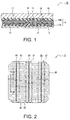
- FIG. 1 is a cross-sectional view of the solar cell module 10.
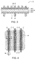
- FIG. 2 is a plan view of a solar cell 11 with metal foils 17 joined thereto, as viewed from the rear surface side
- FIG. 3 is a cross-sectional view along the AA line in FIG. 2 .
- the metal foils 17 are shown with imaginary lines (two-dot chain line) in order to show the current collecting electrodes hidden by the metal foils 17.
- the solar cell module 10 includes a plurality of solar cells 11 each having collector electrodes (not shown in FIG. 1 ), and a plurality of wiring members 15 connecting the adjacent solar cells 11 to each other.
- the solar cell module 10 also includes a plurality of metal foils 17 provided at intervals from each other on the rear surface side of the solar cells 11, at positions overlapping the wiring members 15, and electrically connecting the collector electrodes and the wiring members 15.
- the metal foils 17 are generally lower in resistance (higher in conductivity) than the collector electrodes, and hence the formation of low resistance conductive paths through the intermediary of the metal foils 17 can reduce the serial resistance of the module.
- a metal foil 17 is provided between the rear surface of each of the solar cells 11 and the wiring member 15.
- the metal foil 17 can be said to be a constituent element of the solar cell 11.
- the solar cell 11 provided with the metal foils 17 is sometimes referred to as the solar cell 11 with metal foils.
- the metal foils 17 are not provided on the light receiving surface side of the solar cell 11, but are provided only on the rear surface side of the solar cell 11, in consideration of shadow loss.
- the "light receiving surface" of each of the photoelectric conversion part, the solar cell and the solar cell module means the surface on which sunlight is mainly incident (exceeding 50%), and the "rear surface” means the surface opposite to the light receiving surface.
- the solar cell module 10 includes a first protection member 12 provided on the light receiving surface side of the solar cells 11, a second protection member 13 provided on the rear surface side of the solar cells 11, and a sealing material 14 filled between the protection members.
- the plurality of the solar cells 11 are sealed with the sealing material 14 between the first protection member 12 and the second protection member 13.
- the sealing material 14 includes, for example, a first sealing material 14a provided between the solar cells 11 and the first protection member 12, and a second sealing material 14b provided between the solar cells 11 and the second protection member 13.
- the solar cell module 10 is generally produced by laminating the thin plate-like or film-like constituent members.
- a member having transparency such as a glass substrate, a resin substrate, or a resin sheet can be used.
- a glass substrate For the second protection member 13, the same transparent member as the first protection member 12 or an opaque member may be used.
- a glass substrate is used for the first protection member 12, and a resin film is used for the second protection member 13.
- an olefin resin or a copolymer between ⁇ -olefin and a carboxylic acid vinyl ester such as ethylene-vinyl acetate copolymer (EVA) is used.
- EVA ethylene-vinyl acetate copolymer
- the solar cell module 10 has a string 19 formed by connecting the adjacent solar cells 11 to each other with wiring members 15.
- the string 19 is a unit formed of a plurality of solar cells 11 arranged so as to form a line and electrically connected to each other with wiring members 1.
- the plurality of solar cells 11 are serially connected to each other with the wiring members 15.
- the wiring members 15 are bent between the adjacent solar cells 11 in the thickness direction of the solar cell module 10, in such a way that the wiring members are fitted to the light receiving surface of one of the adjacent solar cells 11 and the rear surface of the other of the adjacent solar cells 11.
- a plurality of the wiring members 15 are fitted to each of the solar cells 11 (see FIG. 4 presented below).
- the adjacent solar cells 11 are connected to each other with the three wiring members 15.
- the wiring member 15 is a belt-like conductive metal wire constituted by a metal such as copper, aluminum, silver, or an alloy including at least one of these metals.
- the width of the wiring member 15 is 10 mm to 30 mm, and the thickness of the wiring member 15 is 20 ⁇ m to 40 ⁇ m.
- the wiring member 15 may be fitted to the light receiving surface and the rear surface of the solar cell 11 with solder, and is preferably fitted with an adhesive 16 (see FIG. 5 presented below).
- the adhesive 16 may be either a conductive adhesive including conductive particles or an insulating adhesive constituted only with a resin component. However, at least the adhesive applied to the light receiving surface is preferably a transparent insulating adhesive.
- the conductive particles may include metal particles such as silver particles, copper particles and nickel particles, carbon particles, and mixtures of these particles. Preferable among these are silver particles.
- the solar cell 11 has a photoelectric conversion part 20 to produce carriers by receiving sunlight, and pluralities of collector electrodes formed respectively on the light receiving surface and the rear surface of the photoelectric conversion part 20.
- the shape of the photoelectric conversion part 20 is not particularly limited, and in the example shown in FIG. 2 , the photoelectric conversion part 20 has an octagonal shape. In other words, the photoelectric conversion part 20 has an approximately square shape in plan view with oblique sides at four corners.
- the collector electrodes are each a fine wire-shaped electrode to collect the carriers generated in the photoelectric conversion part 20, and are preferably formed on a wide range on each of the light receiving surface and the rear surface. The carriers collected by the collector electrodes are taken out to the outside through the wiring members 15.
- the photoelectric conversion part 20 preferably has a semiconductor substrate 20a, and amorphous semiconductor layers 20b and 20c formed on the substrate.
- the semiconductor substrate 20a may include semiconductor wafers made of crystalline silicon (c-Si), gallium arsenide (GaAs) and indium phosphide (InP).
- the crystalline silicon wafer is preferable among these, and an n-type single crystalline silicon wafer is particularly preferable.
- a photoelectric conversion part having a structure in which on the light receiving surface of an n-type single crystalline silicon wafer, an i-type amorphous silicon layer and a p-type amorphous silicon layer are sequentially formed, and on the rear surface, an i-type amorphous silicon layer and an n-type amorphous silicon layer are sequentially formed.
- the photoelectric conversion part 20 preferably has transparent conductive layers 21 and 24 respectively formed on the amorphous semiconductor layers 20b and 20c.
- the transparent conductive layers 21 and 24 are each constituted with a transparent conductive oxide formed by doping, for example, tin (Sn) or antimony (Sb) in a metal oxide such as indium oxide (In 2 O 3 ) or zinc oxide (ZnO).
- the transparent conductive layers 21 and 24 are preferably formed on the light receiving surface and the rear surface of the photoelectric conversion part 20, respectively in such a way that the transparent conductive layers are each formed on almost the whole area of the surface involved except for the edges of the surface involved.
- a plurality of finger electrodes 22 and a plurality of bus bar electrodes are formed on the light receiving surface of the photoelectric conversion part 20, as collector electrodes.
- a plurality of finger electrodes 25 and a plurality of bus bar electrodes 26 are formed respectively as the collector electrodes.
- the pluralities of the finger electrodes 22 and 25 are formed respectively in the wide ranges on the transparent conductive layers 21 and 24. In each of the pluralities of the finger electrodes, the finger electrodes all extend in the same direction, and are formed so as to be approximately parallel to each other at approximately equal intervals from each other.
- Each of the plurality of the bus bar electrodes 26 is formed in a state of being approximately perpendicular to each of the finger electrodes 25 (this is also the case for the bus bar electrodes on the light receiving surface side).
- three bus bar electrodes 26 are formed so as to be approximately parallel to each other at approximately equal intervals from each other.
- the collector electrodes may have a constitution free from bus bar electrodes (for example, see FIG. 9 presented below).
- the finger electrodes 25 are preferably formed in larger areas than the finger electrodes 22.
- the finger electrodes 25 are formed wider in width than the finger electrodes 22, and additionally, larger in number than the finger electrodes 22.
- the finger electrodes 22 are formed thicker than the finger electrodes 25.
- the finger electrodes 25 and the bus bar electrodes 26 both have approximately the same thickness.
- the finger electrodes 22 and the bus bar electrodes (not shown) on the light receiving surface side have also approximately the same thickness.
- the thickness of the finger electrodes 25 and the thickness of the bus bar electrodes 26 are thinner than the thickness of the wiring members 15.
- the width of the bus bar electrodes 26 is preferably smaller than the width of the wiring members 15.
- the wiring members 15 are disposed in the lengthwise direction of the bus bar electrodes 26, above the bus bar electrodes 26 (see FIG. 5 presented below).
- the wiring members 15 are fitted to the rear surface of the solar cells 11, in a state of covering the whole of the bus bar electrodes 26.
- the collector electrodes each have, for example, a structure in which the conductive particles are dispersed in a binder resin, and can be formed by printing a conductive paste on the photoelectric conversion part 20.
- a preferable content of the conductive particles is 60% by mass to 90% by mass in relation to the total weight of the collector electrodes.
- the binder resin may include thermosetting resins such as an epoxy resin, a urethane resin, a urea resin, an acrylic resin, an imide resin and a phenolic resin.
- the collector electrodes can be formed by a plating method, but are preferably formed by a printing method using a conductive paste from the viewpoint of productivity.
- the solar cell module 10 includes the first protection member 12 having transparency, disposed on the light receiving surface side, the second protection member 13 disposed on the rear surface side, and the string 19 provided between the first protection member 12 and the second protection member 13.
- the string 19 includes a plurality of the solar cells 11 each having a plurality of finger electrodes 25 formed so as to be approximately parallel to each other on the rear surface of the photoelectric conversion part 20, a plurality of the wiring members 15, and a plurality of the metal foils 17.
- the wiring members 15 are fitted to each of the solar cells 11 in the direction intersecting the plurality of the finger electrodes 25 and connect the adjacent solar cells 11 to each other.
- the metal foils 17 are provided on the rear surface side of the photoelectric conversion part 20, at intervals from each other, at positions overlapping the wiring members 15 and in a direction intersecting the plurality of the finger electrodes 25, and electrically connect the plurality of the finger electrodes 25 and the wiring members 15.
- FIG. 4 is a diagram illustrating the state of fitting the wiring members 15 to the solar cell 11 with metal foils.
- FIG. 5 is a cross-sectional view along the BB line in FIG. 4 .
- the metal foils 17 are metal thin films electrically connecting the collector electrodes formed on the rear surface of the photoelectric conversion part 20 and the wiring members 15, and a plurality of the metal foils 17 are provided at intervals from each other in a state of overlapping the wiring members 15.
- the current of the finger electrodes 25 is concentrated and the current density becomes high, and hence by increasing the current paths between the collector electrodes and the wiring members 15 through the intermediary of the metal foils 17, by providing the metal foils 17, the serial resistance of the string 19 can be reduced.
- the increase of the current paths due to the metal foils 17 decreases the electrical resistance between the whole of the collector electrodes and the wiring members 15.
- the metal foils 17 may be provided in a state of covering the wiring members 15. Also, in this case, part of the metal foils 17 are disposed on the collector electrodes, and the electrical connection between the collector electrodes and the wiring members 15 through the intermediary of the metal foils 17 is formed. However, the thickness of the wiring members 15 is thicker than the thickness of the collector electrodes, and hence when the metal foils 17 are disposed on the wiring members 15, large cavities (air bubbles) tend to be present between the rear surface of the photoelectric conversion part 20 and the metal foils 17. When cavities are present, for example, exterior appearance faults such as the expansion of the second protection member 13 or the detachment of the sealing material 14 are sometimes caused in the laminating step or the subsequent curing step. Additionally, when the metal foils 17 are disposed on the wiring members 15, pressure is applied to the wiring members 15 and the solar cells 11 are sometimes damaged.
- the metal foils 17 are preferably provided between the rear surface side of the photoelectric conversion part 20 and the wiring members 15.
- the metal foils 17 are provided in a state of being sandwiched by the finger electrodes 25 and the bus bar electrodes 26, the collector electrodes formed on the transparent conductive layer 24 constituting the rear surface of the photoelectric conversion part 20 and the wiring members 15.
- the metal foils 17 reliably intervene between the collector electrodes formed on the transparent conductive layer 24 and the wiring members 15, and the collector electrodes and the wiring members 15 are not brought into direct contact with each other.
- the metal foils 17 are preferably provided so as not to extend outside the rear surface of the photoelectric conversion part 20, in consideration of the prevention of the short-circuiting between the light receiving surface and the rear surface of the solar cell 11.
- the metal foils 17 are formed, for example, in a belt-like form, and are provided in a state of being approximately perpendicular to the finger electrodes 25 in the lengthwise direction of the wiring members 15.
- the metal foils 17 are wider in width than the bus bar electrodes 26, and are longer in length than the bus bar electrodes 26 (see FIG. 2 ).
- the metal foils 17 have a long and narrow, approximately rectangular shape having an approximately constant width W 17 , but the shape of the metal foil is not limited to this (see, for example, FIGS. 7 and 8 presented below).
- the metal foils 17 may have approximately the same shapes and the same dimensions as each other, or alternatively different shapes and different dimensions from each other.
- the same number of the metal foils 17 as the number of the wiring members 15 fitted to the rear surface of the solar cell 11 are provided.
- the metal foils 17 are disposed at intervals from each other, and on the rear surface of the solar cell 11, the rear surface (transparent conductive layer 24) of the photoelectric conversion part 20 is exposed between the collector electrodes in the region free from the metal foils 17.
- the metal foils 17 are preferably provided on almost the whole area of the region (hereinafter, sometimes referred to as the "overlapping region") covered with the wiring members 15, on the rear surface of the solar cell 11. Moreover, it is preferable that the width W 17 of the metal foils 17 (the length in the widthwise direction of the wiring members 15) is longer than the width W 15 of the wiring members 15, and the metal foils 17 are provided in a state in which the metal foils 17 protrude outside the overlapping region of the wiring members 15, from both widthwise ends of the wiring members 15. The wiring members 15 are fitted to the widthwise central parts of the metal foils 17,.
- the provision of the metal foils 17 so as to protrude from the overlapping region of the wiring members 15 leads to shadow loss, but the provision of the metal foils 17 in this portion is effective for the reduction of the serial resistance because in the part of the finger electrodes 25, in the proximity of the wiring members 15, the current of the finger electrodes 25 is concentrated and the current density is high.
- the metal foils 17 are provided in a state of covering the whole of the bus bar electrodes 26 and part of all the finger electrodes 25 connected to the bus bar electrodes.
- the width W 17 of the metal foil 17 is, for example, 10 mm to 20 mm.
- the width W 17 of the metal foils 17 is preferably 1.5 to 10 times and more preferably 2 to 7 times the width W 15 of the wiring members 15.
- the ratio of the width W 17 of the metal foils 17 to the width W 15 of the wiring members 15 is made to fall within the aforementioned range, the shadow loss and the reduction of the serial resistance can be made more efficiently compatible with each other.
- an interval approximately corresponding to the width of one metal foil 17 is provided between the metal foils 17, for example.
- the metal foils 17 are metal thin films constituted by, for example, aluminum, copper, silver or nickel, or alloys mainly composed of these metals. In consideration of the material cost and conductivity, it is preferable to use metal foils 17 made of aluminum or an aluminum alloy.
- the thickness of the metal foils 17 is not particularly limited, but is preferably 30 ⁇ m or less.
- the metal foils 17 are preferably made to adhere to the collector electrodes by using the adhesive 18.
- the adhesive 18 may be either a conductive adhesive including the conductive particles or an insulating adhesive constituted by only a resin component, and may be either an adhesive formed in a film shape or a liquid adhesive.
- a metal foil with an adhesive layer in which a layer of the adhesive 18 is preliminarily formed on one surface of the metal foil it is possible to use, for example, a metal foil with an adhesive layer in which a layer of the adhesive 18 is preliminarily formed on one surface of the metal foil.
- the preferable resin component of the adhesive 18 examples include an olefin resin and a copolymer of an ⁇ -olefin and a carboxylic acid such as an ethylene-vinyl acetate copolymer (EVA).
- EVA ethylene-vinyl acetate copolymer
- a resin of the same type as the sealing material 14 may also be used.
- the adhesive 18 may include a white pigment such as titanium oxide for the purpose of reflecting the light transmitting the photoelectric conversion part 20 so as to be again made incident on the photoelectric conversion part 20.
- the adhesive 18 When an insulating adhesive is used as the adhesive 18, a thin film of the adhesive 18 is formed between the collector electrode and the metal foil 17 to such an extent that the electrical connection between the finger electrode 25 and the metal foil 17 is not impaired.
- the adhesive 18 interposed between the collector electrode and the metal foil 17 may be thicker than when the insulating adhesive is used.
- the adhesive 18 is extruded, for example, between the collector electrode and the metal foil 17, part of the collector electrode is brought into contact with the metal foil 17 without intermediary of the adhesive 18, and a large amount of the adhesive 18 is present between the transparent conductive layer 24 and the metal foil 17.
- the adhesive 18 is preferably filled between the transparent conductive layer 24 and the metal foil 17, without forming a gap, in the gaps between the finger electrodes 25.
- the wiring members 15 are fitted by using an adhesive 16.
- the adhesive 16 for example, an insulating film-shaped or liquid adhesive can be used.
- the adhesive 16 is disposed between the wiring members 15 and the metal foils 17.
- a larger fraction of the adhesive 16 is extruded from between the wiring members 15 and the metal foils 17 and adheres to the sides of the wiring members 15.
- a thin film of the adhesive 16 is formed between the wiring members 15 and the metal foils 17 to an extent that does not impair the electrical connection between the wiring members 15 and the metal foils 17, and the metal foils 17 are partially brought into contact with the wiring members 15 without the intermediary of the adhesive 16.
- the solar cell module 10 provided with the above-described constitution, by forming a low-resistance conductive path in the portion where the current density is high and the current gathers, by providing the metal foils 17 electrically connecting the collector electrodes and the wiring members 15 at the positions overlapping the wiring members 15, it is possible to reduce the serial resistance of the module.
- the plurality of the metal foils 17 are provided at intervals from each other on the rear surface side of the photoelectric conversion part 20, accordingly it is made possible to receive light from the rear surface side of the solar cells 11, and thus the reduction of the serial resistance can be achieved while the shadow loss is being suppressed.
- the solar cell module 10 for example, the light incident from the rear surface side of the module or the light incident from the light receiving surface side of the module and reflected by the second protection member 13, the second sealing material 14b or the like can be utilized for power generation.
- FIG. 6 to FIG. 9 are each diagrams for illustrating another example of the embodiments.
- FIG. 6 to FIG. 8 are plan views respectively illustrating the metals foils 17A, 17B and 17C disposed on the collector electrodes, and each show the wiring member 15 with an imaginary line.
- the metal foil 17A is different from metal foil 17 in that a plurality of through holes 30 are formed in the metal foil 17A.
- cavities air bubbles
- exterior appearance faults such as expansion of the second protection member 13 or detachment of the sealing material 14 are caused, as described above in the lamination step or the subsequent curing step.
- the thickness of the collector electrodes formed on the rear surface of the photoelectric conversion part 20 is thinner compared with the thickness of the wiring members 15, and hence large cavities are hardly generated between the rear surface of the photoelectric conversion part 20 and the metal foils 17A.
- the formation of the through holes 30 functioning as air vent holes allows the occurrence of the cavities to be more reliably suppressed.
- pluralities of approximately circular through holes 30 are formed on both widthwise sides of the metal foil 17A not overlapping the wiring members 15.
- the pluralities of the through holes 30 are formed at approximately equal intervals in the lengthwise direction and in a zigzag pattern without being aligned in the widthwise direction of the metal foil 17A.
- the through holes 30 may be disposed in such a way that the through holes each have a diameter smaller than the spacing between the finger electrodes 25, and the through holes do not overlap the finger electrodes 25.
- the shape and the disposition of the through holes 30 are not limited to the shape and the disposition shown in FIG. 6 .
- a plurality of metal foils 17B are disposed in one line in the lengthwise direction of the wiring members 15.
- the length of the metal foils 17B in the direction along the lengthwise direction of the wiring members 15 is shorter than the length of the bus bar electrodes 26.
- the length of the metal foils 17B in the widthwise direction of the wiring members 15 is longer than the width W 15 of the wiring members 15, and the metal foils 17B protrude from both widthwise edges of the wiring members 15 toward outside the overlapping region. In this case, by decreasing the dimension of one metal foil 17B, the occurrence of the cavities is suppressed.
- the shape of the metal foils 17B is not limited to the approximately rectangular shape as shown in FIG. 7 , and the respective metal foils 17B may also be connected to each other.
- a plurality of through holes 31 functioning as air vent holes are formed in the metal foil 17C.
- the plurality of the through holes 31 are arranged respectively in the widthwise direction and in the lengthwise direction of the metal foil 17C, and are formed in approximately rectangular shapes.
- the metal foil 17C has the width and the length similar to the width and the length of the metal foil 17A, but a plurality of recesses 32 are formed at the edges of the metal foil 17C and the metal foil 17C is wholly formed in a lattice form.
- FIG. 9 is a diagram illustrating the formation pattern of the collector electrodes of the solar cell 11D with metal foils.
- the metal foil 17 is shown by an imaginary line, and the wiring member 15 is omitted.
- the extending direction of the finger electrodes 25D is taken as the X-direction.
- finger electrodes 25D which are the collector electrodes, are formed respectively in a first region Z1 covered with the metal foil 17 of the rear surface of the photoelectric conversion part 20 and a second region Z2 other than the first region Z1.
- the ratio (a1/A1) of the total area (a1) of the collector electrodes formed in the first region Z1 to the total area (A1) of the first region Z1 is smaller than the ratio (a2/A2) of the total area (a2) of the collector electrodes formed in the second region Z2 to the total area (A2) of the second region Z2.
- the solar cell 11D is different from the solar cell 11 in that the solar cell 11D has no bus bar electrodes 26.
- some of the finger electrodes 25D are formed continuously so as to widthwise cross the first region Z1, from the second region Z2 on the one side in the X-direction to the second region Z2 on the other side in the X-direction, and the rest of the finger electrodes 25D are divided into the finger electrodes 25d1 and the finger electrodes 25d2.
- the finger electrodes 25d1 and 25d2 are formed, for example, on the same straight lines.
- some of the finger electrodes 25D are continuously formed on the transparent conductive layer 24 from one end in the X-direction to the other end in the X-direction, while the rest of the finger electrodes 25D are each divided in the first region Z1.
- the solar cell 11D tends to warp toward the rear surface side having a larger electrode area.
- the structure allowing at least some of the finger electrodes 25D to be divided in the first region Z1 allows such warping to be suppressed. As described below, the material cost can also be reduced.
- the finger electrodes 25d1 are formed over from the second region Z2 on one side in the X-direction to one widthwise edge of the first region Z1, and the finger electrodes 25d2 are formed over from the second region Z2 on the other side in the X-direction to the other widthwise edge of the first region Z1.
- Pluralities of the lengthwise ends of the finger electrodes 25d1 and 25d2 are connected to both widthwise edges of the metal foil 17.
- the metal foil 17 is provided in a state of overlapping the lengthwise ends of the finger electrodes 25d1 and 25d2.
- the carriers collected by the finger electrodes 25d1 and 25d2 move from both widthwise edges of the metal foil 17, through the intermediary of the metal foil 17, to the wiring members 15.
- the width and the thickness of the finger electrodes 25D are approximately the same in all the finger electrodes inclusive of the finger electrodes 25d1 and 25d2.
- the area density of the collector electrodes in the first region Z1 is smaller than the area density of the collector electrodes in the second region Z2.
- the area density of the collector electrodes means the total weight of the collector electrodes formed in the object region (such as the first region Z1) per the total area of the object region.
- the metal foil 17 is high in conductivity, and hence when the area density of the collector electrodes in the first region Z1 is reduced, or for example, the area ratio (a1/A1) is reduced, the serial resistance of the module can be reduced.
- the area density of the collector electrodes in the first region Z1 is reduced, the amount of the conductive paste used is reduced, and the material cost can be reduced.
- the finger electrodes 25D extending from the second region Z2 on one side in the X-direction are formed so that only 1 in 2 of the finger electrodes 25 D cross the first region Z1 widthwise.
- a proportion is not particularly limited, but is preferably approximately 1/4 to 9/10.
- At least some of the collector electrodes formed in the first region Z1 may be made thinner than the collector electrodes formed in the second region Z2, and a reduction in the number of the collector electrodes and thinning of the collector electrodes may also be combined.
- a plurality of collector electrodes not connected to the collector electrodes extending from the second region Z2 may also be formed.
- the collector electrodes may also be formed in island-like shapes.
- the collector electrodes formed in island-like shapes are preferably fine-wire shaped electrodes in the X-direction, similarly to the finger electrodes 25D. In these cases, by reducing the area density of the collector electrodes in the first region Z1, it is also possible to reduce the material cost while the reduction of the serial resistance is being achieved.
Landscapes
- Photovoltaic Devices (AREA)
- Life Sciences & Earth Sciences (AREA)
- Engineering & Computer Science (AREA)
- Sustainable Development (AREA)
- Sustainable Energy (AREA)
Applications Claiming Priority (1)
| Application Number | Priority Date | Filing Date | Title |
|---|---|---|---|
| JP2015190404A JP2017069291A (ja) | 2015-09-28 | 2015-09-28 | 太陽電池モジュール |
Publications (1)
| Publication Number | Publication Date |
|---|---|
| EP3147953A1 true EP3147953A1 (fr) | 2017-03-29 |
Family
ID=57003439
Family Applications (1)
| Application Number | Title | Priority Date | Filing Date |
|---|---|---|---|
| EP16190777.9A Withdrawn EP3147953A1 (fr) | 2015-09-28 | 2016-09-27 | Module de cellule solaire |
Country Status (3)
| Country | Link |
|---|---|
| US (1) | US20170092797A1 (fr) |
| EP (1) | EP3147953A1 (fr) |
| JP (1) | JP2017069291A (fr) |
Families Citing this family (2)
| Publication number | Priority date | Publication date | Assignee | Title |
|---|---|---|---|---|
| WO2017154384A1 (fr) * | 2016-03-10 | 2017-09-14 | 株式会社カネカ | Module de cellule solaire |
| KR20250032469A (ko) * | 2023-08-31 | 2025-03-07 | 엘지디스플레이 주식회사 | 터치 표시 장치 |
Citations (3)
| Publication number | Priority date | Publication date | Assignee | Title |
|---|---|---|---|---|
| JP2005167158A (ja) | 2003-12-05 | 2005-06-23 | Sharp Corp | 太陽電池セルおよび太陽電池モジュール |
| WO2013048759A2 (fr) * | 2011-09-29 | 2013-04-04 | Dow Global Technologies Llc | Interconnexion de cellule photovoltaïque |
| WO2014119252A1 (fr) * | 2013-02-01 | 2014-08-07 | 三洋電機株式会社 | Procédé de production pour module de cellules solaires et dispositif de production de module de cellules solaires |
Family Cites Families (2)
| Publication number | Priority date | Publication date | Assignee | Title |
|---|---|---|---|---|
| DE102004013833B4 (de) * | 2003-03-17 | 2010-12-02 | Kyocera Corp. | Verfahren zur Herstellung eines Solarzellenmoduls |
| JP5025135B2 (ja) * | 2006-01-24 | 2012-09-12 | 三洋電機株式会社 | 光起電力モジュール |
-
2015
- 2015-09-28 JP JP2015190404A patent/JP2017069291A/ja active Pending
-
2016
- 2016-09-27 EP EP16190777.9A patent/EP3147953A1/fr not_active Withdrawn
- 2016-09-27 US US15/277,415 patent/US20170092797A1/en not_active Abandoned
Patent Citations (4)
| Publication number | Priority date | Publication date | Assignee | Title |
|---|---|---|---|---|
| JP2005167158A (ja) | 2003-12-05 | 2005-06-23 | Sharp Corp | 太陽電池セルおよび太陽電池モジュール |
| WO2013048759A2 (fr) * | 2011-09-29 | 2013-04-04 | Dow Global Technologies Llc | Interconnexion de cellule photovoltaïque |
| WO2014119252A1 (fr) * | 2013-02-01 | 2014-08-07 | 三洋電機株式会社 | Procédé de production pour module de cellules solaires et dispositif de production de module de cellules solaires |
| US20150340543A1 (en) * | 2013-02-01 | 2015-11-26 | Panasonic Intellectual Property Management Co., Ltd. | Production method for solar cell module and production device for solar cell module |
Also Published As
| Publication number | Publication date |
|---|---|
| JP2017069291A (ja) | 2017-04-06 |
| US20170092797A1 (en) | 2017-03-30 |
Similar Documents
| Publication | Publication Date | Title |
|---|---|---|
| JP5687506B2 (ja) | 太陽電池及び太陽電池モジュール | |
| US10593820B2 (en) | Solar cell module and method for manufacturing same | |
| JP5874011B2 (ja) | 太陽電池及び太陽電池モジュール | |
| US9728658B2 (en) | Solar cell module | |
| JP6065009B2 (ja) | 太陽電池モジュール | |
| US8969708B2 (en) | Solar cell module | |
| CN102593204B (zh) | 太阳能电池和制造该太阳能电池的方法 | |
| JP7146805B2 (ja) | 太陽電池およびその太陽電池を備えた電子機器 | |
| US20220149215A1 (en) | Method for manufacturing solar cell, solar cell, solar cell device, and solar cell module | |
| US20150263194A1 (en) | Solar cell | |
| CN107318269B (zh) | 太阳能电池及其制造方法、太阳能电池模块、以及布线板 | |
| JP5299975B2 (ja) | 裏面電極型太陽電池セル、配線シート、配線シート付き太陽電池セルおよび太陽電池モジュール | |
| US8420927B2 (en) | Solar cell, method of manufacturing the same, and solar cell module | |
| EP3151287A1 (fr) | Module de cellule solaire | |
| KR20140095658A (ko) | 태양 전지 | |
| EP3147953A1 (fr) | Module de cellule solaire | |
| US20200168751A1 (en) | Solar cell and solar cell module | |
| US20150083187A1 (en) | Solar cell module and solar cell module manufacturing method | |
| EP2736082A2 (fr) | Module photoélectrique | |
| JP7626750B2 (ja) | 太陽電池および太陽電池製造方法 | |
| JP5906422B2 (ja) | 太陽電池及び太陽電池モジュール | |
| CN114303250A (zh) | 优化的太阳能电池、太阳能电池模块及其制造方法 | |
| JP6681607B2 (ja) | 太陽電池セルおよび太陽電池セルの製造方法 | |
| JP2020167334A (ja) | 太陽電池セル | |
| KR20150083746A (ko) | 인터커넥터 및 이를 구비한 태양전지 모듈 |
Legal Events
| Date | Code | Title | Description |
|---|---|---|---|
| PUAI | Public reference made under article 153(3) epc to a published international application that has entered the european phase |
Free format text: ORIGINAL CODE: 0009012 |
|
| 17P | Request for examination filed |
Effective date: 20160927 |
|
| AK | Designated contracting states |
Kind code of ref document: A1 Designated state(s): AL AT BE BG CH CY CZ DE DK EE ES FI FR GB GR HR HU IE IS IT LI LT LU LV MC MK MT NL NO PL PT RO RS SE SI SK SM TR |
|
| AX | Request for extension of the european patent |
Extension state: BA ME |
|
| STAA | Information on the status of an ep patent application or granted ep patent |
Free format text: STATUS: THE APPLICATION IS DEEMED TO BE WITHDRAWN |
|
| 18D | Application deemed to be withdrawn |
Effective date: 20170930 |