EP3148065B1 - Dispositif d'alimentation électrique - Google Patents
Dispositif d'alimentation électrique Download PDFInfo
- Publication number
- EP3148065B1 EP3148065B1 EP15796125.1A EP15796125A EP3148065B1 EP 3148065 B1 EP3148065 B1 EP 3148065B1 EP 15796125 A EP15796125 A EP 15796125A EP 3148065 B1 EP3148065 B1 EP 3148065B1
- Authority
- EP
- European Patent Office
- Prior art keywords
- current
- transformers
- power supply
- supply device
- circuit
- Prior art date
- Legal status (The legal status is an assumption and is not a legal conclusion. Google has not performed a legal analysis and makes no representation as to the accuracy of the status listed.)
- Active
Links
Images


Classifications
-
- H—ELECTRICITY
- H02—GENERATION; CONVERSION OR DISTRIBUTION OF ELECTRIC POWER
- H02M—APPARATUS FOR CONVERSION BETWEEN AC AND AC, BETWEEN AC AND DC, OR BETWEEN DC AND DC, AND FOR USE WITH MAINS OR SIMILAR POWER SUPPLY SYSTEMS; CONVERSION OF DC OR AC INPUT POWER INTO SURGE OUTPUT POWER; CONTROL OR REGULATION THEREOF
- H02M1/00—Details of apparatus for conversion
- H02M1/14—Arrangements for reducing ripples from DC input or output
-
- H—ELECTRICITY
- H02—GENERATION; CONVERSION OR DISTRIBUTION OF ELECTRIC POWER
- H02M—APPARATUS FOR CONVERSION BETWEEN AC AND AC, BETWEEN AC AND DC, OR BETWEEN DC AND DC, AND FOR USE WITH MAINS OR SIMILAR POWER SUPPLY SYSTEMS; CONVERSION OF DC OR AC INPUT POWER INTO SURGE OUTPUT POWER; CONTROL OR REGULATION THEREOF
- H02M1/00—Details of apparatus for conversion
- H02M1/08—Circuits specially adapted for the generation of control voltages for semiconductor devices incorporated in static converters
-
- H—ELECTRICITY
- H02—GENERATION; CONVERSION OR DISTRIBUTION OF ELECTRIC POWER
- H02M—APPARATUS FOR CONVERSION BETWEEN AC AND AC, BETWEEN AC AND DC, OR BETWEEN DC AND DC, AND FOR USE WITH MAINS OR SIMILAR POWER SUPPLY SYSTEMS; CONVERSION OF DC OR AC INPUT POWER INTO SURGE OUTPUT POWER; CONTROL OR REGULATION THEREOF
- H02M3/00—Conversion of DC power input into DC power output
- H02M3/01—Resonant DC/DC converters
-
- H—ELECTRICITY
- H02—GENERATION; CONVERSION OR DISTRIBUTION OF ELECTRIC POWER
- H02M—APPARATUS FOR CONVERSION BETWEEN AC AND AC, BETWEEN AC AND DC, OR BETWEEN DC AND DC, AND FOR USE WITH MAINS OR SIMILAR POWER SUPPLY SYSTEMS; CONVERSION OF DC OR AC INPUT POWER INTO SURGE OUTPUT POWER; CONTROL OR REGULATION THEREOF
- H02M3/00—Conversion of DC power input into DC power output
- H02M3/22—Conversion of DC power input into DC power output with intermediate conversion into AC
- H02M3/24—Conversion of DC power input into DC power output with intermediate conversion into AC by static converters
- H02M3/28—Conversion of DC power input into DC power output with intermediate conversion into AC by static converters using discharge tubes with control electrode or semiconductor devices with control electrode to produce the intermediate AC
- H02M3/285—Single converters with a plurality of output stages connected in parallel
-
- H—ELECTRICITY
- H02—GENERATION; CONVERSION OR DISTRIBUTION OF ELECTRIC POWER
- H02M—APPARATUS FOR CONVERSION BETWEEN AC AND AC, BETWEEN AC AND DC, OR BETWEEN DC AND DC, AND FOR USE WITH MAINS OR SIMILAR POWER SUPPLY SYSTEMS; CONVERSION OF DC OR AC INPUT POWER INTO SURGE OUTPUT POWER; CONTROL OR REGULATION THEREOF
- H02M3/00—Conversion of DC power input into DC power output
- H02M3/22—Conversion of DC power input into DC power output with intermediate conversion into AC
- H02M3/24—Conversion of DC power input into DC power output with intermediate conversion into AC by static converters
- H02M3/28—Conversion of DC power input into DC power output with intermediate conversion into AC by static converters using discharge tubes with control electrode or semiconductor devices with control electrode to produce the intermediate AC
- H02M3/325—Conversion of DC power input into DC power output with intermediate conversion into AC by static converters using discharge tubes with control electrode or semiconductor devices with control electrode to produce the intermediate AC using devices of a triode or a transistor type requiring continuous application of a control signal
- H02M3/335—Conversion of DC power input into DC power output with intermediate conversion into AC by static converters using discharge tubes with control electrode or semiconductor devices with control electrode to produce the intermediate AC using devices of a triode or a transistor type requiring continuous application of a control signal using semiconductor devices only
- H02M3/33538—Conversion of DC power input into DC power output with intermediate conversion into AC by static converters using discharge tubes with control electrode or semiconductor devices with control electrode to produce the intermediate AC using devices of a triode or a transistor type requiring continuous application of a control signal using semiconductor devices only of the forward type
- H02M3/33546—Conversion of DC power input into DC power output with intermediate conversion into AC by static converters using discharge tubes with control electrode or semiconductor devices with control electrode to produce the intermediate AC using devices of a triode or a transistor type requiring continuous application of a control signal using semiconductor devices only of the forward type with automatic control of the output voltage or current
-
- H—ELECTRICITY
- H02—GENERATION; CONVERSION OR DISTRIBUTION OF ELECTRIC POWER
- H02M—APPARATUS FOR CONVERSION BETWEEN AC AND AC, BETWEEN AC AND DC, OR BETWEEN DC AND DC, AND FOR USE WITH MAINS OR SIMILAR POWER SUPPLY SYSTEMS; CONVERSION OF DC OR AC INPUT POWER INTO SURGE OUTPUT POWER; CONTROL OR REGULATION THEREOF
- H02M3/00—Conversion of DC power input into DC power output
- H02M3/22—Conversion of DC power input into DC power output with intermediate conversion into AC
- H02M3/24—Conversion of DC power input into DC power output with intermediate conversion into AC by static converters
- H02M3/28—Conversion of DC power input into DC power output with intermediate conversion into AC by static converters using discharge tubes with control electrode or semiconductor devices with control electrode to produce the intermediate AC
- H02M3/325—Conversion of DC power input into DC power output with intermediate conversion into AC by static converters using discharge tubes with control electrode or semiconductor devices with control electrode to produce the intermediate AC using devices of a triode or a transistor type requiring continuous application of a control signal
- H02M3/335—Conversion of DC power input into DC power output with intermediate conversion into AC by static converters using discharge tubes with control electrode or semiconductor devices with control electrode to produce the intermediate AC using devices of a triode or a transistor type requiring continuous application of a control signal using semiconductor devices only
- H02M3/33569—Conversion of DC power input into DC power output with intermediate conversion into AC by static converters using discharge tubes with control electrode or semiconductor devices with control electrode to produce the intermediate AC using devices of a triode or a transistor type requiring continuous application of a control signal using semiconductor devices only having several active switching elements
- H02M3/33571—Half-bridge at primary side of an isolation transformer
-
- H—ELECTRICITY
- H02—GENERATION; CONVERSION OR DISTRIBUTION OF ELECTRIC POWER
- H02M—APPARATUS FOR CONVERSION BETWEEN AC AND AC, BETWEEN AC AND DC, OR BETWEEN DC AND DC, AND FOR USE WITH MAINS OR SIMILAR POWER SUPPLY SYSTEMS; CONVERSION OF DC OR AC INPUT POWER INTO SURGE OUTPUT POWER; CONTROL OR REGULATION THEREOF
- H02M1/00—Details of apparatus for conversion
- H02M1/0003—Details of control, feedback or regulation circuits
- H02M1/0009—Devices or circuits for detecting current in a converter
-
- H—ELECTRICITY
- H02—GENERATION; CONVERSION OR DISTRIBUTION OF ELECTRIC POWER
- H02M—APPARATUS FOR CONVERSION BETWEEN AC AND AC, BETWEEN AC AND DC, OR BETWEEN DC AND DC, AND FOR USE WITH MAINS OR SIMILAR POWER SUPPLY SYSTEMS; CONVERSION OF DC OR AC INPUT POWER INTO SURGE OUTPUT POWER; CONTROL OR REGULATION THEREOF
- H02M1/00—Details of apparatus for conversion
- H02M1/0043—Converters switched with a phase shift, i.e. interleaved
-
- H—ELECTRICITY
- H02—GENERATION; CONVERSION OR DISTRIBUTION OF ELECTRIC POWER
- H02M—APPARATUS FOR CONVERSION BETWEEN AC AND AC, BETWEEN AC AND DC, OR BETWEEN DC AND DC, AND FOR USE WITH MAINS OR SIMILAR POWER SUPPLY SYSTEMS; CONVERSION OF DC OR AC INPUT POWER INTO SURGE OUTPUT POWER; CONTROL OR REGULATION THEREOF
- H02M1/00—Details of apparatus for conversion
- H02M1/0048—Circuits or arrangements for reducing losses
- H02M1/0054—Transistor switching losses
- H02M1/0058—Transistor switching losses by employing soft switching techniques, i.e. commutation of transistors when applied voltage is zero or when current flow is zero
-
- H—ELECTRICITY
- H02—GENERATION; CONVERSION OR DISTRIBUTION OF ELECTRIC POWER
- H02M—APPARATUS FOR CONVERSION BETWEEN AC AND AC, BETWEEN AC AND DC, OR BETWEEN DC AND DC, AND FOR USE WITH MAINS OR SIMILAR POWER SUPPLY SYSTEMS; CONVERSION OF DC OR AC INPUT POWER INTO SURGE OUTPUT POWER; CONTROL OR REGULATION THEREOF
- H02M1/00—Details of apparatus for conversion
- H02M1/0064—Magnetic structures combining different functions, e.g. storage, filtering or transformation
-
- Y—GENERAL TAGGING OF NEW TECHNOLOGICAL DEVELOPMENTS; GENERAL TAGGING OF CROSS-SECTIONAL TECHNOLOGIES SPANNING OVER SEVERAL SECTIONS OF THE IPC; TECHNICAL SUBJECTS COVERED BY FORMER USPC CROSS-REFERENCE ART COLLECTIONS [XRACs] AND DIGESTS
- Y02—TECHNOLOGIES OR APPLICATIONS FOR MITIGATION OR ADAPTATION AGAINST CLIMATE CHANGE
- Y02B—CLIMATE CHANGE MITIGATION TECHNOLOGIES RELATED TO BUILDINGS, e.g. HOUSING, HOUSE APPLIANCES OR RELATED END-USER APPLICATIONS
- Y02B70/00—Technologies for an efficient end-user side electric power management and consumption
- Y02B70/10—Technologies improving the efficiency by using switched-mode power supplies [SMPS], i.e. efficient power electronics conversion e.g. power factor correction or reduction of losses in power supplies or efficient standby modes
Definitions
- the present invention relates to power supply devices.
- a resonant switching power supply controls a current or a voltage into a sine wave, and performs switching with either the current or the voltage almost equal zero. This helps dramatically reduce switching loss and noise.
- serial resonant switching power supply being a current-voltage resonant circuit, not only helps reduce switching loss but also operates with a smaller surge in the circuit and achieves higher efficiency compared with other circuit designs such as a phase-shift full-bridge design. Because of these benefits, serial resonant switching power supplies have been introduced in many appliances like as power supplies in liquid crystal television sets and servers.
- the output voltage is adjusted through pulse frequency modulation control (PFM control) by switching elements.
- PFM control pulse frequency modulation control
- Si-based IGBTs insulated-gate bipolar transistors
- the tail currents that occur when they are turned OFF make it impossible to cope with higher frequencies, and this leads to an unduly large size in isolation transformers.
- Si-based MOSFETs metal-oxide-semiconductor field-effect transistors
- the upper limit of the input voltage that can be input to the serial resonant switching power supply is about 400 V.
- serial resonant circuits are connected in parallel for increased output power.
- the ripple currents in their outputs add up to a high ripple current (e.g., Patent Document 1).
- the transformer that serves to isolate the primary and secondary sides of the main circuit from each other has a special shape, and this prevents the transformer from being made compact.
- the present invention aims to provide a power supply device that can achieve a balance among the currents respectively passing through serial resonant circuits connected in parallel, without an unnecessary increase in circuit scale.
- a power supply device includes: three resonant DC-DC converter phases which are connected in parallel between an input node of a DC input voltage and an output node of a DC output voltage and of which the operation phases are displaced from each other by 120 degrees.
- the resonant DC-DC converter phases respectively include: switching circuits which convert DC to AC by switching the DC input voltage by using first switching elements respectively; serial resonant circuits which are connected to output nodes of the switching circuits respectively; and rectifying-smoothing circuits which are connected to output nodes of the serial resonant circuits respectively.
- the serial resonant circuits respectively include first transformers, second transformers, and resonance capacitors.
- the primary windings of the first transformers, the primary windings of the second transformers, and the resonance capacitors are connected in series with each other respectively.
- the secondary windings of the second transformers are connected to the rectifying-smoothing circuits respectively.
- the first transformers respectively include separate cores, and respectively have the primary and secondary windings isolated from each other with leakage inductances present between the primary and secondary windings.
- the secondary windings of different phases are connected in parallel with each other.
- the first transformers may respectively have the primary and secondary windings isolated by split bobbins. (A second configuration.)
- the power supply device may further include: a current detection circuit which is provided on the secondary winding side of the first transformers and which detect the currents that pass through the secondary windings; and a control circuit which monitors the resonance state and also controls and protects the first switching elements in accordance with the result of detection by the current detection circuit.
- the power supply device may further include: second switching elements which are respectively provided on the secondary winding side of the first transformers and which respectively short-circuit the secondary windings of the first transformers in accordance with a current balance control signal. (A fourth configuration.)
- the current balance control signal may have, when the power supply device is in a light-load condition, such a logic level as to let the secondary windings be short-circuited.
- the first switching elements may all be SiC-based MISFETs (metal-insulator-semiconductor field-effect transistors). (A sixth configuration.)
- the DC output voltage may have a voltage value equal to the voltage value of the DC input voltage.
- the rectifying-smoothing circuits may be of a full-wave rectification type. (An eighth configuration.)
- the rectifying-smoothing circuits may respectively include SiC-based Schottky barrier diodes as rectifying elements. (A ninth configuration.)
- the power supply device may further include: a DC power supply circuit which produces the DC input voltage from a commercial AC voltage. (A tenth configuration.)
- the power supply device may further include: a checker configured to check whether or not a current-balancing operation is normal based on whether or not current oscillation at a frequency other than the resonance frequency of the serial resonant circuits is occurring. (An eleven configuration.)
- Fig. 1 is a circuit diagram showing one configuration example of an LLC resonance DC-DC converter.
- the LLC resonance DC-DC converter (hereinafter abbreviated to "DC-DC converter 10") of this configuration example is a power conversion circuit that receives input of a DC input voltage Vi and outputs a DC output voltage Vo, and includes a switching circuit 11, a serial resonant circuit 12, and a rectifying-smoothing circuit 13.
- the switching circuit 11 includes switching elements Q1 and Q2 that are serially connected between an application node of the input voltage Vi and a ground node (GND1) of a primary circuit system 10p.
- the switching circuit 11 turns ON and OFF the switching elements Q1 and Q2 complementarily to switch the DC input voltage Vi, and thereby converts DC electric power to AC electric power.
- "complementarily” covers not only a configuration where the ON/OFF states of the switching elements are completely reversed but also a configuration where the ON/OFF transitions of the switching elements take place with a delay relative to each other (so that there is a period (dead time) in which they are both OFF).
- the serial resonant circuit 12 is connected to an output node of the switching circuit 11 (a connection node between the switching elements Q1 and Q2).
- the serial resonant circuit 12 electrically isolates the primary circuit system 10p (GND1 system) and a secondary circuit system 10s (GND2 system) from each other by use of an isolation transformer TR1, and meanwhile transfers AC electric power from the primary circuit system 10p to the secondary circuit system 10s.
- the rectifying-smoothing circuit 13 includes rectification diodes D1 and D2 and a smoothing capacitor C1 that are connected to an output node of the serial resonant circuit 12 (the secondary winding of the isolation transformer TR1).
- the rectifying-smoothing circuit 13 rectifies and smooths the AC electric power transferred from the primary circuit system 10p, and thereby produces the DC output voltage Vo.
- the serial resonant circuit 12 includes, as circuit elements involved in its resonating operation, reactances Ls and Lp and resonant capacitors Cr1 and Cr2 (each with a capacitance value Cr).
- reactances Ls and Lp reactances Ls and Lp and resonant capacitors Cr1 and Cr2 (each with a capacitance value Cr).
- a current Is passes via either current path (1) or current path (2) depending on the operating state of the switching circuit 11 (the ON/OFF states of the switching elements Q1 and Q2).
- current path (1) in operation, depending on the resonance state, the secondary circuit system 10s conducts, so that a current passes through the rectification diode D1 via current path (3).
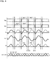
- a component corresponding to the current that passes through current path (3) passes through the reactor Ls while resonating with a resonance period of 2 ⁇ (Ls • Lc) (see the small-dash line in Fig. 2 ).
- the remaining current component passes through the reactor Ls while resonating with a resonance period of 2 ⁇ ((Ls + Lp) • Cr) (see the large-dash line in Fig. 2 ). Accordingly, the current Is, which is the sum of those components, has two resonance frequencies (see the bold solid line in Fig. 2 ).
- the switching element Q1 when the switching element Q1 is turned from ON to OFF as described above, the parasitic capacitance of the switching element Q1 and the reactors Ls and Lp are brought into a state where they are connected in series as seen from a supply power node (the application node of the DC input voltage Vi); accordingly, the voltage across the switching element Q1 rises while resonating (voltage resonance).
- the switching element Q1 when the switching element Q1 is ON, the current that passes through the switching element Q1 is made to resonate by the reactors Ls and Lp and the resonant capacitor Cr2 (current resonance). Based on such behavior, the LLC resonant DC-DC converter 10 can be said to be a current-voltage resonance circuit.
- Fig. 3 is a circuit diagram showing a power supply device 1 according to a first embodiment of the present invention.
- the LLC resonant DC-DC converters 10-* are abbreviated to "DC-DC converters 10-*".
- the DC-DC converters 10-* have a configuration basically similar to that shown in Fig. 1 , and are connected in parallel so as to cope with three phases between an input node of a DC input voltage Vi (e.g., DC 800 V) and an output node of an output voltage Vo (e.g., DC 400 V).
- a DC input voltage Vi e.g., DC 800 V
- an output node of an output voltage Vo e.g., DC 400 V
- the DC power supply circuit 20 feeds the DC input voltage Vi to the DC-DC converters 10-*.
- Usable as the DC power supply circuit 20 is, for example, an AC-DC converter that produces the DC input voltage Vi from a commercial AC supply voltage Vac (e.g., AC 400 V).
- Each DC-DC converter 10-* includes a switching circuit 11-*, a serial resonant circuit 12-*, and a rectifying-smoothing circuit 13-*.
- the switching circuit 11-* is of a half-bridge type that includes a pair of switching elements Q*1 and Q*2 (both corresponding to a first switching element) serially connected between the application node of the input voltage Vi and the ground node (GND1) of a primary circuit system 10p.
- the switching circuit 11-* turns ON and OFF the switching elements complementarily to switch the DC input voltage Vi, and thereby converts DC electric power to AC electric power.
- the switching elements Q*1 and Q*2 are, for example, SiC-based N-channel MISFETs (which will be described in detail later).
- the serial resonant circuit 12-* is connected to an output node of the switching circuit 11-* (a connection node between the switching elements Q*1 and Q*2).
- the serial resonant circuit 12-* electrically isolates the primary circuit system 10p (GND1 system) and a secondary circuit system 10s (GND2 system) from each other, and meanwhile transfers AC electric power from the primary circuit system 10p to the secondary circuit system 10s.
- the serial resonant circuit 12-* includes, as its circuit elements, a first transformer T*1 (corresponding to a balance transformer), which serves for current balancing and resonance, and a second transformer T*2 (corresponding to a main transformer), which serves for input-output isolation and resonance).
- the first and second transformers T*1 and T*2 include primary windings T*1a and T*2a and secondary windings T*1b and T*2b respectively.
- a first end of the primary winding T*1a is connected to the output node of the switching circuit 11-*.
- a second end of the primary winding T*1a is connected to a first end of the primary winding T*2a.
- a second end of the primary winding T*2a is connected via a resonance capacitor C*1 to the application node of the input voltage Vi, and is also connected via a resonance capacitor C*2 to the ground node (GND1) of the primary circuit system 10p. That is, the primary winding T*1a of the first transformer T*1, the primary winding T*2a of the second transformer T*2, and the resonance capacitors C*1 and C*2 are connected in series with each other.
- the secondary winding T*2b of the second transformer T*2 is of a center-tap type, and is connected to the rectifying-smoothing circuit 13-* in the subsequent stage.
- the center tap of the secondary winding T*2b is connected to a ground node (GND2) of the secondary circuit system 10s.
- Each first transformer T*1 has a separate core, and has the primary and secondary windings T*1a and T*1b isolated from each other by a split bobbin.
- the secondary windings T*1b of the respective phases are connected in parallel with each other to form a current-balancing circuit. The operation of the current-balancing circuit will be described in detail later.
- the rectifying-smoothing circuit 13-* includes rectification diodes D*1 and D*2 and a smoothing capacitor Co that are connected to an output node of the serial resonant circuit 12 (the secondary winding T*2b of the second transformer T*2).
- the rectifying-smoothing circuit 13-* rectifies and smooths the AC electric power transferred from the primary circuit system 10p, and thereby produces a DC output voltage Vo.
- An anode of the rectification diode D*1 is connected to a first end of the secondary winding T*2b.
- An anode of the rectification diode D*2 is connected to a second end of the secondary winding T*2b.
- Cathodes of the rectification diodes D*1 and D*2 are both connected to the output node of the DC output voltage Vo.
- the smoothing capacitor Co is shared among the rectifying-smoothing circuits 13-*, and is connected between the output node of the DC output voltage Vo and the ground node (GND2) of the secondary circuit system 10s.
- this configuration example deals with a configuration where the secondary winding T*2b of the second transformer T*2 is of a center-tap type and the rectifying-smoothing circuit 13-* is connected in the stage subsequent to it, this is not meant to limit the configuration of the output stage of the power supply device 1; instead, the secondary winding T*2b of the second transformer T*2 may be of a single-tap type, and the rectifying-smoothing circuit 13-* is connected in the stage subsequent to it.
- period I when the gate-source voltage Vgs11 turns to zero and the switching element Q11 turns OFF, the switch current Iq11 turns to 0 A.
- the drain-source voltage Vds11 of the switching element Q11 varies like a sine wave while resonating, before it eventually reaches the DC input voltage Vi.
- the primary current IL1 is held passing in the same direction as before; thus, the reverse parallel diode (or parasitic diode) of the switching element Q12 turns ON, and the negative-direction switch current Iq12 starts to pass.
- the switch current Iq12 varies from the negative direction to the positive direction while resonating at a resonance frequency that depends on the leakage inductance of the first transformer T11, the leakage inductance of the second transformer T12, the excitation inductance of the second transformer T12, and the capacitance value of the resonance capacitor C11.
- the switching element Q12 ON during a period in which the switch current Iq12 has a negative value ( ⁇ 0 A), it is possible to achieve ZVS.
- period III when an induced voltage occurring in the secondary winding T12b of the second transformer T12 rises and the rectification diode D12 is brought into a forward-biased state, the secondary current Id12 passes while resonating at a resonance frequency that depends on the leakage inductance of the first transformer T11, the leakage inductance of the second transformer T12, and the capacitance value of the resonance capacitor C11.
- the output currents Io* produced by the DC-DC converters 10-* respectively have, when considered on a phase-by-phase basis, a period in which a current passes like a sine wave and a period in which no current passes. Attempting to smooth these currents individually requires large-capacity smoothing capacitors. Seeing that the operation phases of the DC-DC converters 10-* are displaced from each other by 120 degrees, with the three phases considered in parallel, the sum of the output currents Io* (i.e., the eventual output current Io) is always equal to the value observed when the currents passing in the respective phases are equal, and the ripples that occur are small. Accordingly, by, instead of smoothing the output currents Io* individually, smoothing the output current Io, which is their sum, it is possible to reduce the capacitance value of the smoothing capacitor Co.
- Fig. 5 is a first diagram (a diagram showing the secondary windings T*1b of the respective phases as they alone are extracted) in illustration of current-balancing operation.
- Fig. 6 is a second diagram (a conceptual diagram showing the balance currents I* passing through the secondary windings T*1b of the respective phases in the form of vectors) in illustration of current-balancing operation.
- the vector sum of the balance currents I* equals zero, and thus the absolute values of the balance currents I* are unambiguously equal. Accordingly, making the turn ratios of the first transformers T*1 of the respective phases equal results in making the primary currents IL* passing through the primary windings T*1a of the respective phases equal, and it is then possible to achieve current-balancing operation.
- the number of parallel connected DC-DC converters 10-* has to be three (or a multiple of three).
- six-phase DC-DC converters can be divided into two sets each comprising three-phase DC-DC converters, and for each set, the three-phase DC-DC converters can be controlled with their operation phases displaced from each other by 120 degrees. In that case, it does not matter whether the operation phases of the different sets are identical or not.
- Fig. 7 is a third diagram (a circuit diagram of the first transformers T*1 of the respective phases as they alone are extracted) in illustration of current-balancing operation.
- the symbol Lp*a represents the excitation inductances on the primary side
- the symbol Lp*b represents the excitation inductances on the secondary side.
- the symbol Ls* represents the leakage inductances on the primary side.
- the leakage inductances Ls* of the first transformers T*1 can be used as resonance reactors for the serial resonant circuits 12-*. This permits the leakage inductances of the second transformers T*2 to be designed to be lower than is conventionally usual. Distributing part of the resonance conditions to the first transformers T*1 in this way helps alleviate the restrictions on the leakage inductances of the second transformers T*2, and thus helps achieve size reduction in the second transformers T*2.
- the first transformers T*1 each have a separate core, and have the primary and secondary windings T*1a and T*1b structurally separated from each other by a split bobbin. With this structure, it is possible to obtain high leakage inductances Ls* in the first transformers T*1 and to adjust them individually according to the circuit constant errors in the respective phases, and it is thus possible to suppress variation of the output voltage Vo due to current-balancing operation among the different phases resulting from uneven resonance conditions.
- Fig. 8 is a schematic diagram showing one configuration example of a split bobbin used in the first transformer T*1.
- box (A) is a top view (a view from above) of the split bobbin 100; in box (B) is a side view of the split bobbin 100; and in box (C) is a longitudinal sectional view of the split bobbin 100 and a core 200 (a longitudinal sectional view of the first transformer T*1).
- the split bobbin 100 is an electrically insulating member (e.g., a member formed of plastic) that has a top portion 101, a bottom portion 102, a splitting portion 103, a first reel portion 104, a second reel portion 105, and a cavity portion 106.
- the first reel portion 104, around which a primary winding L1 (corresponding to the primary winding T*1a mentioned previously) is wound, and the second reel portion 105, around which a secondary winding L2 (corresponding to the secondary winding T*1b mentioned previously) is wound, are structurally isolated from each other by the splitting portion 103.
- the primary and secondary windings L1 and L2 be designed such that whichever is subjected to a higher current is given a larger thickness.
- the turn ratio of the first transformer T*1 is so designed as to handle a high voltage with a low current on the primary winding T*1a side and a low voltage with a high current at the secondary winding T*1b side, it can be said that it is preferable that the secondary winding L2 be designed to be thicker than the primary winding L1.
- the core 200 is composed of a pair of E-shaped core members 210 and 220 that form a closed magnetic circuit by holding the split bobbin 100 from opposite sides, that is, from above and below.
- the E-shaped core members 210 and 220 respectively have middle leg portions 211 and 221 and side leg portions 212 and 222.
- the middle leg portions 211 and 221 are each a circular cylinder-form member that is inserted into the cavity portion 106 of the split bobbin 100.
- the side leg portions 212 and 222 are each a wall-form member that rises so as to surround the middle leg portions 211 or 221 and that entirely or partly covers the circumferential rims of the split bobbin 100.
- the middle leg portions 211 and 221 are inserted into the cavity portion 106 in the split bobbin 100 such that the tip faces of the middle leg portions 211 and 221 abut on each other.
- the side leg portions 212 and 222 entirely or partly cover the circumferential rims of the split bobbin 100 such that the tip faces of the side leg portions 212 and 222 abut on each other.
- the leakage inductance Ls* of the first transformer T*1 can be increased and decreased by appropriately trimming the tip faces of the middle leg portions 211 and 221 and thereby adjusting the gap portion 230 (gap width) between them.
- the split bobbin 100 By forming the first transformers T*1 by use of the split bobbin 100 configured as described above, it is possible to obtain high leakage inductances Ls* in the first transformers T*1, and to adjust them individually according to the circuit constant errors in the respective phases.
- Si-based IGBTs or MOSFETs SiC-based MISFETs, which have higher withstand voltages (e.g., resistant to up to 900 V to 1200 V) and which are capable of high-frequency operation.
- a wide-bandgap semiconductor such as SiC has a high dielectric breakdown electric-field intensity (in contrast to 0.3 MV/cm with Si, 2.8 MV/cm with SiC). This allows, when fabricating FETs, a design with a small thickness in a withstand voltage retention drift layer combined with a high carrier concentration. Accordingly, with the same chip area, a SiC-based chip has a lower ON-state resistance than (one-tenth of) that of a Si-based chip; that is, the former provides the same ON-state resistance with a smaller chip area. It is thus possible to reduce the parasitic capacitances of FETs and achieve fast operation. With the same carrier concentration profile, a SiC-based chip provides a higher device withstand voltage than that of a Si-based chip.
- SiC-based MISFETs as the switching elements Q*1 and Q*2 makes it possible to accept input of a higher DC input voltage Vi than when Si-based MOSFETs are used, and makes it possible to set the switching frequency higher than when Si-based IGBTs are used. In this way, it is possible to build a compact, high-capacity power supply device 1 without unnecessarily increasing the number of parallel connected DC-DC converters 10-*.
- the number of parallel connected DC-DC converters 10-* has to be three (or a multiple of three), and this imposes a limit in increasing the electric power handled so long as Si-based MOSFETs are used as the switching elements Q*1 and Q*2.
- SiC-based MISFETs as the switching elements Q*1 and Q*2
- the switching frequency has to be set at, for example, 20 kHz or less. Accordingly, to reduce the use magnetic flux density in the second transformers T*2, it is necessary to increase the effective cross-sectional area of the cores or increase the number of turns of the primary and secondary windings T*2a and T*2b, leading to an increased size in the second transformers T*2.
- the switching frequency can be set at, for example, 150 kHz or more, and this helps reduce the use magnetic flux density in the second transformers T*2 and suppress their magnetic saturation without unnecessarily increasing the effective cross-sectional area of the cores or the number of turns in the windings. It can be said that this, in combination with the previously-mentioned distribution of part of resonance reactors to the first transformers T*1, is highly effective in achieving a smaller size in the second transformers T*2.
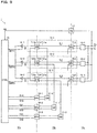
- Fig. 9 is a circuit diagram showing a power supply device 1 according to a second embodiment of the present invention.
- the power supply device 1 of this embodiment has a configuration basically similar to that in the first embodiment described previously, and is characterized in additionally including current detection circuits 14-* on the secondary winding T*1b side of the first transformers T*1. Accordingly, such components as find their counterparts in the first embodiment are identified by the same reference signs as in Fig. 3 , and no overlapping description will be repeated; the following description focuses on the features unique to the second embodiment.
- the power supply device 1 of the second embodiment includes, in addition to the circuit elements of the DC-DC converters 10-*, namely the switching circuits 11-*, the serial resonant circuits 12-*, and the rectifying-smoothing circuits 13-*, current detection circuits 14-*, a control circuit 15, insulated-gate driver circuits 16-*, and an output feedback circuit 17.
- the current detection circuits 14-* are provided in a control circuit system 10c (on the secondary winding T*1b side of the first transformers T*1), which is electrically isolated from the primary and second circuit systems 10p and 10s.
- the current detection circuits 14-* detect the balance currents I* passing through the secondary windings T*1b respectively to produce balance current detection signals DET*, and feed these to the control circuit 15.
- the control circuit 15 is provided in the control circuit system 10c, and functions as the principal controlling agent of the switching circuits 11-*. More specifically, the control circuit 15 produces gate signals G*1 and G*2 having a frequency commensurate with a feedback signal FB fed from the output feedback circuit 17, and feeds them via the insulated-gate driver circuits 16-* to the switching circuits 11-* (and hence to the switching elements Q*1 and Q*2). Through output feedback control like this, the desired output voltage Vo can be produced.
- the control circuit 15 also has the functions of, in accordance with the balance current detection signals DET* fed from the current detection circuits 14-*, monitoring the resonance state and controlling and protecting the switching elements Q*1 and Q*2. For example, in a case where the serial resonant circuits 12-* have gone into an abnormally resonant state, or the balance currents I* (and hence the primary currents IL* and hence the switch currents Iq*1 and Iq*2 passing through the switching elements Q*1 and Q*2) have gone into an overcurrent state, the control circuit 15 can forcibly stop the ON-OFF operation of the switching elements Q*1 and Q*2, and this helps enhance the safety of the power supply device 1.
- the insulated-gate driver circuits 16-* electrically isolate the control circuit system 10c and the primary circuit system 10p from each other, and meanwhile deliver the gate signals G*1 and G*2 from the control circuit 15 to the switching circuits 11-*.
- the output feedback circuit 17 electrically isolates the secondary circuit system 10s and the control circuit system 10c from each other, and meanwhile generates a feedback signal FB in accordance with the output voltage Vo and transfers it to the control circuit 15.
- control circuit 15 the insulated-gate driver circuits 16-*, and the output feedback circuit 17 are provided also in the first embodiment described previously (through not illustrated in Fig. 3 for the sake of convenient illustration).
- the primary and secondary windings T*1a and T*1b of the first transformers T*1 are structurally separated from each other by the split bobbin 100 (see Fig. 8 ).
- the primary circuit system 10p and the control circuit system 10c are electrically isolated from each other completely. Accordingly, providing the current detection circuits 14-* in the control circuit system 10c makes it possible to safely and individually detect the balance currents I* passing in the respective phases (and hence the primary currents IL* and hence the switch currents Iq*1 and Iq*2 passing through the switching elements Q*1 and Q*2).
- the DC input voltage Vi is very high, and it is therefore preferable that the current detection circuits 14-* and the control circuit 15 be electrically isolated from the primary circuit system 10p.
- additional circuits such as the current detection circuits 14-* be attached not to the second transformers T*2 for input-output isolation and resonance but to the first transformers T*1 for current balancing and resonance.
- the second transformers T*2 do not have to be given a special structure, and thus their size can be reduced. It can be said that this, in combination with the previously mentioned distribution of part of resonance reactors to the first transformers T*1 and the previously mentioned adoption of SiC-based MISFETs for faster switching, is highly effective in reducing the size of the second transformers T*2.
- Fig. 10 is a circuit diagram showing a power supply device 1 according to a third embodiment of the present invention.
- the power supply device 1 of the third embodiment has a configuration basically similar to that in the first embodiment described previously, and is characterized by additionally including a current balance control circuit 18 on the secondary winding T*1b side of the first transformers T*1. Accordingly, such components as find their counterparts in the first embodiment are identified by the same reference signs as in Fig. 3 , and no overlapping description will be repeated; the following description focuses on the features unique to the third embodiment.
- the current balance control circuit 18 includes a switching element Q41 (corresponding to a second switching element) and diodes D41 and D42.
- the switching element Q41 for example, an N-channel MOSFET can be suitably used.
- the addition of the current balance control circuit 18 is accompanied by the replacement of the secondary windings T*1b of all the first transformers T*1 with windings of a center-tap type.
- a drain of the switching element Q41 is connected to cathodes of the diodes D41 and D42.
- a source of the switching element Q41 is connected to the center taps of the secondary windings T*1b (the ground node GND1 of the primary circuit system 10p).
- a current balance control signal Sbc is applied to a gate of the switching element Q41.
- An anode of the diode D41 is connected to the first ends of the secondary windings T*1b.
- An anode of the diode D42 is connected to the second ends of the secondary windings T*1b.
- the current balance control circuit 18 configured as described above, by turning the switching element Q41 ON, it is possible to short-circuit the secondary windings T*1b, and thereby to stop the current-balancing operation described previously.
- the diodes D41 and D42 are provided to inhibit a current that tends to pass through the body diode of the switching element Q41.
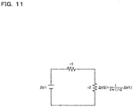
- Fig. 11 is an equivalent circuit diagram in illustration of output variation under a light load (corresponding to an equivalent circuit diagram of the power supply device 1).
- the electromotive forces that occur in the excitation inductances Lp*a and Lp*b when the primary currents IL* of the respective phases differ appear to cause the leakage inductances Ls* of the first transformers T*1 to increase and decrease. That is, in a phase where the primary current IL* is lower, current balancing operates in such a direction as to decrease the leakage inductance Ls* and increase the primary current IL*; reversely, in a phase where the primary current IL* is higher, current balancing operates in such a direction as to increase the leakage inductance Ls* and decrease the primary current IL*.
- the output impedance r1 of the power supply device 1 is a variable parameter ( ⁇ Ls*) ascribable to inductors, and varies as the leakage inductances Ls* increase and decrease.
- the output impedance r1 basically exhibits a high value to the amount of the variation ⁇ V2 (with a switching frequency f of the order of megahertz) in the DC output voltage Vo that results from current-balancing operation. Accordingly, under a heavy load, even when current-balancing operation causes variation in the output impedance r1, this hardly affects the amount of variation ⁇ V2.
- variation in the output impedance r1 that accompanies current-balancing operation appears as the amount of the variation ⁇ V2 in the DC output voltage Vo.
- This phenomenon (a rise in output under a light load) occurs precisely because current-balancing operation is performed.
- the load state the magnitude of the input current I ⁇
- the control circuit 15 switching the logic level of the current balance control signal Sbc in such a manner that the secondary windings T*1b are short-circuited and thereby current-balancing operation is suspended when the power supply device 1 is in a light-load condition, it is possible to avoid the above-mentioned phenomenon (a rise in output under a light load).
- the primary and secondary windings T*1a and T*1b are structurally separated from each other by use of the split bobbin 100 (see Fig. 8 ), and thus the control for suspending the current-balancing function can be performed safely in the control circuit system 10c, which is electrically isolated from the primary circuit system 10p.
- Fig. 12 is a circuit diagram showing a power supply device 1 according to a fourth embodiment of the present invention.
- the power supply device 1 of the fourth embodiment has a configuration basically similar to that in the third embodiment described previously, and is characterized by being configured to produce a DC output voltage Vo that has the same voltage value as the DC input voltage Vi (configured simply to isolate the primary circuit system 10p and the secondary circuit system 10s from each other). Accordingly, such components as find their counterparts in the third embodiment are identified by the same reference signs as in Fig. 10 , and no overlapping description will be repeated; the following description focuses on the features unique to the third embodiment.
- two serially connected second transformers T*2X and T*2Y with a turn ratio of 1:1 are used as main transformers for input-output isolation and resonance, and the configuration of the rectifying-smoothing circuits 13-* has been changed.
- the second transformers T*2X and T*2Y include primary windings T*2Xa and T*2Ya and secondary windings T*2Xb and T*2Yb respectively.
- First ends of the primary windings T*2Xa are connected to the primary windings T*1a of the first transformers T*1.
- Second ends of the primary windings T*2Xa are connected to first ends of the primary windings T*2Ya.
- Second ends of the primary windings T*2Ya are connected to the resonance capacitors C*1 and C*2.
- the rectifying-smoothing circuits 13-* include rectification diodes D*3 and D*4, one each for each phase, and smoothing capacitors Co1 and Co2, common to all the phases.
- Anodes of the rectification diodes D*3 and cathodes of the rectification diodes D*4 are all connected to first ends of the secondary windings T*2Xb. Second ends of the secondary windings T*2Xb are connected to first ends of the secondary windings T*2Yb.
- Cathodes of the rectification diodes D*3 are connected to the output node of the output voltage Vo.
- Anodes of the rectification diodes D*4 are connected to the ground node (GND2) of the secondary circuit system 10s.
- a first end of the smoothing capacitor Co1 is connected to the output node of the DC output voltage Vo.
- a second end of the smoothing capacitor Co1 and a first end of the smoothing capacitor Co2 are both connected to second ends of the secondary windings T*2Yb.
- a second end of the smoothing capacitor Co2 is connected to the ground node (GND2) of the secondary circuit system 10s.
- the power supply device 1 With the circuit configuration described above, the power supply device 1 according to the fourth embodiment produces a DC output voltage Vo that has the same voltage value as the DC input voltage Vi, and simply isolates the primary circuit system 10p and the secondary circuit system 10s from each other.
- the DC output voltage Vo is higher than in the first to third embodiments, and thus as the rectification diodes D*3 and D*4, it is preferable to use SiC-based Schottky barrier diodes or the like, which have a high withstand voltage (resistant to up to 900 V to 1200 V) combined with a low forward voltage drop.
- SiC-based Schottky barrier diodes or the like which have a high withstand voltage (resistant to up to 900 V to 1200 V) combined with a low forward voltage drop.
- the power supply device 1 as main transformers for input-output isolation and resonance, two serially connected second transformers T*2X and T*2Y are used. With this configuration, it is possible to reduce the voltage applied to each transformer to one-half, and thus to disperse the generated heat and avoid magnetic saturation.
- the size of the main transformers can be reduced satisfactorily by (1) distributing part of resonance reactors to the first transformers T*1, (2) adopting SiC-based MISFETs for higher switching, and (3) simplifying the second transformers T*2 by adding a circuit to the first transformers T*1. Accordingly, dividing the main transformers into two second transformers T*2X and T*2Y does not result in making them unduly bulky.
- Fig. 13 is a table showing the measurement conditions. As shown there, in the experiments, operating waveforms at relevant points were actually measured while the power supply device 1 according to the fourth embodiment was operated with the following settings: input/output voltages, 600 V; output power, 5 kW; and switching frequency, 182 kHz.
- SiC-based MOSFETs used as the primary-side switching elements Q*1 and Q*2 were SiC-based MOSFETs (with a withstand voltage of 1200V and a withstand current of 40 A), and used as the secondary-side rectification diodes D*3 and D*4 were SiC-based SBDs (Schottky barrier diodes) (with a withstand voltage of 1200V and a withstand current of 10 A).
- SiC-based SBDs Schottky barrier diodes
- the resonance capacitors C*1 and C*2 each had a capacitance of 60 nF.
- the composite excitation inductances provided by the two transformers T*2X and T*2Y for the respective phases (phases 1, 2, and 3) were 110.7 ⁇ H, 116.1 ⁇ H, and 113.7 ⁇ H respectively.
- the composite leakage inductances provided by the first transformers T*1 and the two second transformers T*2X and T*2Y for the respective phases (phases 1, 2, and 3) were 12.0 ⁇ H, 11.6 ⁇ H, and 11.6 ⁇ H respectively.
- the errors among the inductance values in the respective phases occurred unintentionally during fabrication.
- Fig. 14 is an actually measured waveform diagram showing the drain current Id (right-hand vertical axis) and the drain-source voltage Vds (left-hand vertical axis) of the primary-side SiC MOSFET.
- the drain current Id corresponds to the switch current Iq12 mentioned previously
- the drain-source voltage Vds corresponds to the drain-source voltage Vds12 mentioned previously.
- the actually measured waveforms shown in Fig. 14 agree well with the simulation waveforms shown in the timing chart in Fig. 4 .
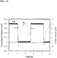
- Fig. 15 is an actually measured waveform diagram, similar to Fig. 14 , obtained when the power supply device 1 according to the fourth embodiment was operated, with a circuit configured with circuit constants similar to those in Fig. 13 , with the following settings: input/output voltages, 800 V; output voltage, 5 kW; and switching frequency, 162 kHz. What is shown there proves that using SiC MOSFETs with a withstand voltage of 1200 V makes it possible to perform operation that cannot be achieved with Si FETs with a withstand voltage of about 900 V.
- Figs. 16 and 17 are actually measured waveform diagrams showing the forward currents through the secondary-side SiC SBDs (in the illustrated example, the rectification diodes D13, D23, and D33) as actually measured under the circuit conditions shown in Fig. 13 .
- Fig. 16 shows a case with no current balancing
- Fig. 17 shows a case with current balancing. From a comparison of the two diagrams, it will be clearly seen that the current-balancing operation described previously makes the forward currents in the respective phases even.
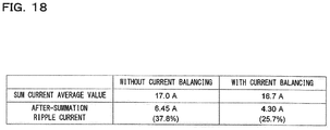
- Fig. 18 is a comparison table of the sum current average value and the after-summation ripple current. As shown there, the sum current average value was 17.0 A without current balancing and 16.7 A with current balancing. The after-summation ripple current was 6.45 A (37.8%) without current balancing and 4.30 A (25.7%) with current balancing. Thus, an improvement was confirmed as to the ripple current.
- the currents can be measured by the current detection circuits 14-* when the power supply device 1 is in actual operation, or the currents through the switching elements or through the rectifying elements can be measured at the time of assembly or operation checking of the power supply device 1, as methods for checking whether or not current oscillation (irregularities in the current waveforms) at a frequency other than the resonance frequency is occurring.
- current oscillation when current balancing is in operation, current oscillation at a frequency different from the switching frequency occurs. Accordingly, based on whether or not there is current oscillation, it is possible to easily check whether or not the current-balancing circuit is operating normally, and to properly discriminate a fault in the circuit and enhance the reliability of the power supply device 1.
- a checker can be provided that is configured to perform automatically a checking process as described above when the power supply device 1 is started up or operated in a test mode and then feed the results to a host (such as a microcomputer provided outside the power supply device 1).
- the control circuit 15 described previously may be equipped with the function of such a checker.
- a checking process as described above may be performed from outside the power supply device 1 at the time of inspection or the like of the power supply device 1 prior to shipment.
- Power supply devices find applications as isolated power supply devices in industrial machinery and infrastructure equipment, and can be suitably used for the purpose of isolating, in particular, appliances that use commercial AC power sources around AC 400 V.
Landscapes
- Engineering & Computer Science (AREA)
- Power Engineering (AREA)
- Dc-Dc Converters (AREA)
Claims (7)
- Dispositif d'alimentation électrique (1) comprenant :trois phases de convertisseur continu-continu à résonance (10-1, 10-2, 10,-3), qui sont raccordées en parallèle entre un noeud d'entrée d'une tension continue d'entrée et un noeud de sortie d'une tension continue de sortie et dont des phases de fonctionnement sont déplacées les unes par rapport aux autres de 120 degrés, dans lequelles phases de convertisseur continu-continu à résonance comprennent respectivement :des circuits de commutation (11-1, 11-2, 11-3) qui convertissent le courant continu en courant alternatif en commutant la tension continue d'entrée en utilisant des premiers éléments de commutation (Q11, Q12, Q21, Q22, Q31, Q32) respectivement ;des circuits résonants séries (12-1, 12-2, 12-3) qui sont raccordés à des noeuds de sortie des circuits de commutation respectivement ; etdes circuits de redressement et de lissage (13-1, 13-2, 13-3) qui sont raccordés à des noeuds de sortie des circuits résonants séries respectivement,les circuits résonants séries (12-1, 12-2, 12-3) comprennent respectivement des premiers transformateurs (T11, T21, T31), des seconds transformateurs (T12, T22, T32) et des condensateurs à résonance,des enroulements primaires des premiers transformateurs (T11, T21, T31), des enroulements primaires des seconds transformateurs (T12, T22, T32) et les condensateurs à résonance sont raccordés en série les uns aux autres respectivement,des enroulements secondaires des seconds transformateurs (T12, T22, T32) sont raccordés aux circuits de redressement et de lissage respectivement,les premiers transformateurs (T11, T21, T31) comprennent respectivement des noyaux distincts et comportent respectivement les enroulements primaires et secondaires isolés les uns des autres, des inductances de fuite étant présentes entre les enroulements primaires et secondaires, les enroulements secondaires de différentes phases étant raccordés en parallèle les uns aux autres.
- Dispositif d'alimentation électrique selon la revendication 1, dans lequel
les premiers transformateurs (T11, T21, T31) comportent respectivement les enroulements primaires et secondaires isolés par des bobines fendues. - Dispositif d'alimentation électrique selon la revendication 1 ou 2, comprenant en outre :un circuit de détection de courant (14-1, 14-2, 14-3) qui est disposé côté enroulement secondaire des premiers transformateurs et qui est conçu pour détecter des courants qui passent à travers les enroulements secondaires ; etun circuit de commande (15) qui est conçu pour surveiller un état de résonance et également pour commander et pour protéger les premiers éléments de commutation (Q11, Q12, Q21, Q22, Q31, Q32) en fonction d'un résultat de détection par le circuit de détection de courant.
- Dispositif d'alimentation électrique selon l'une quelconque des revendications 1 à 3, comprenant en outre :
des seconds éléments de commutation (Q41) qui sont respectivement disposés côté enroulement secondaire des premiers transformateurs pour court-circuiter respectivement les enroulements secondaires des premiers transformateurs en fonction d'un signal de commande d'équilibre de courant. - Dispositif d'alimentation électrique selon la revendication 4, dans lequel
le signal de commande d'équilibre de courant présente, lorsque le dispositif d'alimentation électrique (1) est dans une condition de charge légère, un niveau logique de sorte à permettre le court-circuit des enroulements secondaires. - Dispositif d'alimentation électrique selon l'une quelconque des revendications 1 à 5, dans lequel
les premiers éléments de commutation (Q11, Q12, Q21, Q22, Q31, Q32) sont tous des transistors MISFET à base de SiC (des transistors à effet de champ métal-isolant-semi-conducteur). - Dispositif d'alimentation électrique selon l'une quelconque des revendications 1 à 6, comprenant en outre :
un dispositif de vérification configuré pour vérifier si une opération d'équilibrage de courant est, ou non, normale selon qu'une oscillation de courant se produit, ou non, à une fréquence autre qu'une fréquence de résonance des circuits résonants séries.
Applications Claiming Priority (3)
| Application Number | Priority Date | Filing Date | Title |
|---|---|---|---|
| JP2014103284 | 2014-05-19 | ||
| JP2014191190A JP6295173B2 (ja) | 2014-05-19 | 2014-09-19 | 電源装置 |
| PCT/JP2015/064198 WO2015178344A1 (fr) | 2014-05-19 | 2015-05-18 | Dispositif d'alimentation électrique |
Publications (3)
| Publication Number | Publication Date |
|---|---|
| EP3148065A1 EP3148065A1 (fr) | 2017-03-29 |
| EP3148065A4 EP3148065A4 (fr) | 2018-01-17 |
| EP3148065B1 true EP3148065B1 (fr) | 2019-03-13 |
Family
ID=54554014
Family Applications (1)
| Application Number | Title | Priority Date | Filing Date |
|---|---|---|---|
| EP15796125.1A Active EP3148065B1 (fr) | 2014-05-19 | 2015-05-18 | Dispositif d'alimentation électrique |
Country Status (4)
| Country | Link |
|---|---|
| US (1) | US9819275B2 (fr) |
| EP (1) | EP3148065B1 (fr) |
| JP (1) | JP6295173B2 (fr) |
| WO (1) | WO2015178344A1 (fr) |
Families Citing this family (40)
| Publication number | Priority date | Publication date | Assignee | Title |
|---|---|---|---|---|
| EP2299580A3 (fr) * | 2009-06-24 | 2011-07-27 | STMicroelectronics S.r.l. | Convertisseur résonant multiphases et son procédé de contrôle |
| WO2017011008A1 (fr) * | 2015-07-15 | 2017-01-19 | Hewlett-Packard Development Company, L.P. | Alimentation d'un dispositif de surveillance d'énergie |
| JP2017046536A (ja) * | 2015-08-28 | 2017-03-02 | サンケン電気株式会社 | 直流電源装置 |
| JP6409730B2 (ja) * | 2015-10-05 | 2018-10-24 | オムロン株式会社 | 変圧器およびそれを備えた共振型回路 |
| WO2017084716A1 (fr) * | 2015-11-19 | 2017-05-26 | Abb Schweiz Ag | Système convertisseur utilisant des modules convertisseurs |
| CN109874380A (zh) | 2016-07-07 | 2019-06-11 | 华为技术有限公司 | 四开关三相dc-dc谐振转换器 |
| JP6272438B1 (ja) * | 2016-10-27 | 2018-01-31 | 三菱電機株式会社 | 電力変換装置 |
| JP6793941B2 (ja) * | 2016-10-31 | 2020-12-02 | 福島SiC応用技研株式会社 | 加速器 |
| JP6749613B2 (ja) * | 2017-02-07 | 2020-09-02 | ローム株式会社 | 直流電源装置 |
| JP6821493B2 (ja) * | 2017-04-14 | 2021-01-27 | 東芝デベロップメントエンジニアリング株式会社 | 電流共振型dc−dcコンバータ |
| KR102105149B1 (ko) * | 2017-05-26 | 2020-04-28 | 주식회사 솔루엠 | Llc 공진형 컨버터 및 전자장치 |
| JP6395166B1 (ja) * | 2017-07-10 | 2018-09-26 | 三菱電機株式会社 | 電力変換装置 |
| CN109428490B (zh) * | 2017-08-15 | 2020-10-16 | 台达电子企业管理(上海)有限公司 | 多单元功率变换系统 |
| US20190181744A1 (en) * | 2017-12-11 | 2019-06-13 | Texas Instruments Incorporated | Bus converter current ripple reduction |
| KR102063459B1 (ko) * | 2018-08-31 | 2020-01-08 | 주식회사 솔루엠 | Llc 공진형 전력 변환기 |
| JP2020039228A (ja) * | 2018-09-05 | 2020-03-12 | 本田技研工業株式会社 | 電圧変換装置 |
| TWI711259B (zh) * | 2019-05-30 | 2020-11-21 | 亞源科技股份有限公司 | 諧振轉換器 |
| EP3772170A1 (fr) | 2019-07-30 | 2021-02-03 | Delta Electronics (Thailand) Public Co., Ltd. | Convertisseur llc ayant une pluralité d'inverseurs |
| WO2021050912A1 (fr) | 2019-09-13 | 2021-03-18 | Milwaukee Electric Tool Corporation | Convertisseurs de puissance à semi-conducteurs à large bande interdite |
| EP3796529B1 (fr) * | 2019-09-20 | 2023-12-27 | ABB Schweiz AG | Redondance d'un étage de convertisseur résonant par adaptation de la fréquence |
| JP7352179B2 (ja) * | 2020-01-24 | 2023-09-28 | オムロン株式会社 | 過電流保護装置、dc/dcコンバータ装置、及び電力システム |
| DE102020201562A1 (de) * | 2020-02-07 | 2021-08-12 | Dürr Systems Ag | Stromwandlungseinheit und Beschichtungsanlage |
| JP7501172B2 (ja) * | 2020-07-08 | 2024-06-18 | オムロン株式会社 | 電力変換装置及び電力システム |
| JP7599894B2 (ja) | 2020-10-13 | 2024-12-16 | 株式会社東芝 | 電力変換装置 |
| CN112751474B (zh) * | 2020-12-02 | 2022-02-25 | 阳光电源股份有限公司 | 一种三相llc谐振直流变换器 |
| JP7247247B2 (ja) * | 2021-03-11 | 2023-03-28 | 株式会社京三製作所 | 電力変換装置 |
| US12057767B2 (en) * | 2021-05-12 | 2024-08-06 | Maxim Integrated Products, Inc. | Switching power converters including injection stages, and associated methods |
| JP7098025B1 (ja) * | 2021-06-09 | 2022-07-08 | 三菱電機株式会社 | 電力変換装置 |
| US12401286B2 (en) * | 2022-03-09 | 2025-08-26 | Texas Instruments Incorporated | Startup circuit for a flyback converter |
| JP2023132636A (ja) * | 2022-03-11 | 2023-09-22 | 新電元工業株式会社 | 電源装置 |
| DE102022202957A1 (de) | 2022-03-25 | 2023-09-28 | Siemens Aktiengesellschaft | DC/DC-Wandler |
| CN114825940B (zh) * | 2022-04-11 | 2024-05-28 | 南京航空航天大学 | 一种可自动均压的多相输入串联输出并联双有源桥变换器 |
| KR20240053977A (ko) * | 2022-10-18 | 2024-04-25 | 한국전기연구원 | 전압밸런싱회로 및 이를 포함하는 스위치소자 스태킹회로 |
| CN115622410B (zh) * | 2022-10-21 | 2025-07-08 | 苏州浪潮智能科技有限公司 | 一种开关谐振槽变换电路、芯片、主板以及电子设备 |
| US20240162804A1 (en) * | 2022-11-08 | 2024-05-16 | Deere & Company | Reduced energy loss control methods for dc-dc converters |
| JP7481510B1 (ja) * | 2023-01-05 | 2024-05-10 | Necプラットフォームズ株式会社 | 電源回路、電源回路の制御方法、およびプログラム |
| JP2024108803A (ja) | 2023-01-31 | 2024-08-13 | 株式会社日立製作所 | 電力変換装置 |
| JP7781804B2 (ja) * | 2023-03-02 | 2025-12-08 | 株式会社東芝 | 電力変換装置 |
| CN118783754A (zh) * | 2024-09-12 | 2024-10-15 | 深圳麦格米特电气股份有限公司 | 一种电源控制电路、电源控制方法及电子设备 |
| KR102945658B1 (ko) | 2025-10-02 | 2026-03-31 | (주)아이씨디 | 다중연결 구조의 초고주파 파워회로 |
Family Cites Families (25)
| Publication number | Priority date | Publication date | Assignee | Title |
|---|---|---|---|---|
| JP3644615B2 (ja) * | 1997-02-17 | 2005-05-11 | Tdk株式会社 | スイッチング電源 |
| JP4406967B2 (ja) * | 1999-09-03 | 2010-02-03 | サンケン電気株式会社 | 直流電源装置 |
| JP2004254440A (ja) * | 2003-02-20 | 2004-09-09 | Sony Corp | 電源回路 |
| US6970366B2 (en) * | 2003-04-03 | 2005-11-29 | Power-One As | Phase-shifted resonant converter having reduced output ripple |
| JP4485337B2 (ja) * | 2004-12-08 | 2010-06-23 | 株式会社日立製作所 | 電流検出回路、電源制御回路、電源装置、電源システム、および電子装置 |
| DE102005036806A1 (de) * | 2005-08-02 | 2007-02-08 | Lorch Schweißtechnik GmbH | Elektrische Stromquelle, insbesondere Schweißstromquelle |
| US8259477B2 (en) * | 2007-05-30 | 2012-09-04 | The Regents Of The University Of California | Multiphase resonant converter for DC-DC applications |
| WO2009011091A1 (fr) * | 2007-07-18 | 2009-01-22 | Panasonic Corporation | Dispositif d'alimentation électrique à commutation |
| CN101431300B (zh) | 2007-11-07 | 2011-05-18 | 群康科技(深圳)有限公司 | 电源电路及其控制方法 |
| JP4301342B2 (ja) | 2007-12-18 | 2009-07-22 | サンケン電気株式会社 | Dc/dcコンバータ |
| EP2299580A3 (fr) * | 2009-06-24 | 2011-07-27 | STMicroelectronics S.r.l. | Convertisseur résonant multiphases et son procédé de contrôle |
| JP6087628B2 (ja) * | 2010-01-11 | 2017-03-01 | フィリップス ライティング ホールディング ビー ヴィ | Ac/dc変換回路 |
| KR20130073611A (ko) * | 2011-12-23 | 2013-07-03 | 삼성전기주식회사 | 전원 공급 장치 |
| CN102545638B (zh) * | 2012-01-20 | 2016-03-30 | 华为技术有限公司 | 交错并联三电平dc/dc变换器和ac/dc变换器 |
| CN102611315A (zh) * | 2012-03-22 | 2012-07-25 | 华为技术有限公司 | 一种谐振转换电路 |
| CN103780081B (zh) * | 2012-10-22 | 2019-09-13 | 山特电子(深圳)有限公司 | 交错式llc均流变换器 |
| WO2014116641A1 (fr) * | 2013-01-24 | 2014-07-31 | Murata Manufacturing Co., Ltd. | Régulation de courant d'appel lors du démarrage de convertisseurs résonants |
| US9515562B2 (en) * | 2013-03-05 | 2016-12-06 | Futurewei Technologies, Inc. | LLC resonant converters |
| US9240724B2 (en) * | 2013-03-13 | 2016-01-19 | Astec International Limited | Multiphase DC/DC converters and control circuits for controlling converters using fixed and/or variable frequencies |
| FR3004870B1 (fr) * | 2013-04-23 | 2015-05-22 | Valeo Equip Electr Moteur | Procede et dispositif de commande d'un convertisseur multiphase courant continu-courant continu a resonance, et convertisseur multiphase correspondant |
| US9337743B2 (en) * | 2013-10-11 | 2016-05-10 | Futurewei Technologies, Inc. | Apparatus and method for multiple primary bridge resonant converters |
| US9444346B2 (en) * | 2013-10-17 | 2016-09-13 | Futurewei Technologies, Inc. | Apparatus and efficiency point tracking method for high efficiency resonant converters |
| CN103683964A (zh) * | 2013-12-20 | 2014-03-26 | 华为技术有限公司 | 谐振式双向变换器及不间断电源装置、及控制方法 |
| CN106664025B (zh) * | 2014-07-21 | 2019-04-05 | 华为技术有限公司 | 双向dc-dc转换器 |
| EP3133614B1 (fr) * | 2015-08-18 | 2019-11-20 | Delta Electronics (Thailand) Public Co., Ltd. | Composant magnétique intégré |
-
2014
- 2014-09-19 JP JP2014191190A patent/JP6295173B2/ja active Active
-
2015
- 2015-05-18 WO PCT/JP2015/064198 patent/WO2015178344A1/fr not_active Ceased
- 2015-05-18 EP EP15796125.1A patent/EP3148065B1/fr active Active
- 2015-05-18 US US15/303,683 patent/US9819275B2/en not_active Expired - Fee Related
Non-Patent Citations (1)
| Title |
|---|
| None * |
Also Published As
| Publication number | Publication date |
|---|---|
| JP2016001980A (ja) | 2016-01-07 |
| US9819275B2 (en) | 2017-11-14 |
| US20170025963A1 (en) | 2017-01-26 |
| JP6295173B2 (ja) | 2018-03-14 |
| EP3148065A4 (fr) | 2018-01-17 |
| EP3148065A1 (fr) | 2017-03-29 |
| WO2015178344A1 (fr) | 2015-11-26 |
Similar Documents
| Publication | Publication Date | Title |
|---|---|---|
| EP3148065B1 (fr) | Dispositif d'alimentation électrique | |
| US9484821B2 (en) | Adjustable resonant apparatus for power converters | |
| US9337743B2 (en) | Apparatus and method for multiple primary bridge resonant converters | |
| US9178438B2 (en) | Apparatus for resonant converters | |
| US8542501B2 (en) | Switching power-supply apparatus | |
| CA2837698C (fr) | Alimentation electrique a mode resonant dotee d'un inducteur a enroulements multiples | |
| US9515562B2 (en) | LLC resonant converters | |
| US9190911B2 (en) | Auxiliary resonant apparatus for LLC converters | |
| EP2740207B1 (fr) | Procédé permettant de commander une alimentation électrique à mode résonant et alimentation électrique à mode résonant dotée d'un dispositif de commande | |
| EP2975753B1 (fr) | Convertisseur à trois niveaux | |
| Jeon et al. | A primary-side-assisted zero-voltage and zero-current switching three-level DC-DC converter with phase-shift control | |
| Hasan et al. | Design, optimization, and validation of gan-based dab converter for active cell balancing in btms applications | |
| US10804807B2 (en) | Low RMS current zero voltage switching assisting circuit with low power loss and EMI | |
| US11356029B2 (en) | Rectifying circuit and switched-mode power supply incorporating rectifying circuit | |
| Wang et al. | Phase-shift soft-switching power amplifier with lower EMI noise | |
| Zhao et al. | A seven-level switched capacitor ac-dc rectifier for fast wireless charging | |
| Narimani et al. | A comparative study of three-level DC-DC converters | |
| Pastor et al. | Inverter optimization of soft-switching DC-DC converter | |
| Sun et al. | Energy-Based Analysis of Zero-Voltage-Switching in 6.78 MHz 4N-GaN-HEMT Inverters | |
| Almardy et al. | Three-phase (LC)(L)-type series-resonant converter: Design and experimental results | |
| JP2020022307A (ja) | 電源装置及び電源装置の制御方法 | |
| Tolstoy et al. | Dual control used in series-loaded resonant converter with SiC devices | |
| Mirzadarani et al. | Phase-Shift Fixed-Frequency LCLC Resonant Converter: Analysis of Operational Modes and Mitigation of Parallel Capacitance of Output Diodes | |
| Mohseni et al. | Feasibility Study of MHz Switching Frequency Isolated DC-DC Converters | |
| Ji et al. | A Full-Load Range Soft-Switching Method for Full Bridge Converter Based on Small Magnetizing Inductance and Segmented Fixed-Frequency Control |
Legal Events
| Date | Code | Title | Description |
|---|---|---|---|
| STAA | Information on the status of an ep patent application or granted ep patent |
Free format text: STATUS: THE INTERNATIONAL PUBLICATION HAS BEEN MADE |
|
| PUAI | Public reference made under article 153(3) epc to a published international application that has entered the european phase |
Free format text: ORIGINAL CODE: 0009012 |
|
| STAA | Information on the status of an ep patent application or granted ep patent |
Free format text: STATUS: REQUEST FOR EXAMINATION WAS MADE |
|
| 17P | Request for examination filed |
Effective date: 20161115 |
|
| AK | Designated contracting states |
Kind code of ref document: A1 Designated state(s): AL AT BE BG CH CY CZ DE DK EE ES FI FR GB GR HR HU IE IS IT LI LT LU LV MC MK MT NL NO PL PT RO RS SE SI SK SM TR |
|
| AX | Request for extension of the european patent |
Extension state: BA ME |
|
| DAV | Request for validation of the european patent (deleted) | ||
| DAX | Request for extension of the european patent (deleted) | ||
| A4 | Supplementary search report drawn up and despatched |
Effective date: 20171214 |
|
| RIC1 | Information provided on ipc code assigned before grant |
Ipc: H02M 3/337 20060101ALI20171208BHEP Ipc: H02M 3/28 20060101AFI20171208BHEP Ipc: H02M 1/00 20060101ALN20171208BHEP Ipc: H02M 1/14 20060101ALI20171208BHEP |
|
| GRAP | Despatch of communication of intention to grant a patent |
Free format text: ORIGINAL CODE: EPIDOSNIGR1 |
|
| STAA | Information on the status of an ep patent application or granted ep patent |
Free format text: STATUS: GRANT OF PATENT IS INTENDED |
|
| RIC1 | Information provided on ipc code assigned before grant |
Ipc: H02M 3/337 20060101ALI20180831BHEP Ipc: H02M 1/00 20060101ALN20180831BHEP Ipc: H02M 3/28 20060101AFI20180831BHEP Ipc: H02M 1/14 20060101ALI20180831BHEP |
|
| INTG | Intention to grant announced |
Effective date: 20180919 |
|
| RIC1 | Information provided on ipc code assigned before grant |
Ipc: H02M 1/14 20060101ALI20180907BHEP Ipc: H02M 1/00 20060101ALN20180907BHEP Ipc: H02M 3/28 20060101AFI20180907BHEP Ipc: H02M 3/337 20060101ALI20180907BHEP |
|
| GRAS | Grant fee paid |
Free format text: ORIGINAL CODE: EPIDOSNIGR3 |
|
| GRAA | (expected) grant |
Free format text: ORIGINAL CODE: 0009210 |
|
| STAA | Information on the status of an ep patent application or granted ep patent |
Free format text: STATUS: THE PATENT HAS BEEN GRANTED |
|
| AK | Designated contracting states |
Kind code of ref document: B1 Designated state(s): AL AT BE BG CH CY CZ DE DK EE ES FI FR GB GR HR HU IE IS IT LI LT LU LV MC MK MT NL NO PL PT RO RS SE SI SK SM TR |
|
| REG | Reference to a national code |
Ref country code: GB Ref legal event code: FG4D |
|
| REG | Reference to a national code |
Ref country code: CH Ref legal event code: EP Ref country code: AT Ref legal event code: REF Ref document number: 1109043 Country of ref document: AT Kind code of ref document: T Effective date: 20190315 |
|
| REG | Reference to a national code |
Ref country code: DE Ref legal event code: R096 Ref document number: 602015026482 Country of ref document: DE |
|
| REG | Reference to a national code |
Ref country code: IE Ref legal event code: FG4D |
|
| REG | Reference to a national code |
Ref country code: NL Ref legal event code: MP Effective date: 20190313 |
|
| REG | Reference to a national code |
Ref country code: LT Ref legal event code: MG4D |
|
| PG25 | Lapsed in a contracting state [announced via postgrant information from national office to epo] |
Ref country code: SE Free format text: LAPSE BECAUSE OF FAILURE TO SUBMIT A TRANSLATION OF THE DESCRIPTION OR TO PAY THE FEE WITHIN THE PRESCRIBED TIME-LIMIT Effective date: 20190313 Ref country code: LT Free format text: LAPSE BECAUSE OF FAILURE TO SUBMIT A TRANSLATION OF THE DESCRIPTION OR TO PAY THE FEE WITHIN THE PRESCRIBED TIME-LIMIT Effective date: 20190313 Ref country code: NO Free format text: LAPSE BECAUSE OF FAILURE TO SUBMIT A TRANSLATION OF THE DESCRIPTION OR TO PAY THE FEE WITHIN THE PRESCRIBED TIME-LIMIT Effective date: 20190613 Ref country code: FI Free format text: LAPSE BECAUSE OF FAILURE TO SUBMIT A TRANSLATION OF THE DESCRIPTION OR TO PAY THE FEE WITHIN THE PRESCRIBED TIME-LIMIT Effective date: 20190313 |
|
| PG25 | Lapsed in a contracting state [announced via postgrant information from national office to epo] |
Ref country code: GR Free format text: LAPSE BECAUSE OF FAILURE TO SUBMIT A TRANSLATION OF THE DESCRIPTION OR TO PAY THE FEE WITHIN THE PRESCRIBED TIME-LIMIT Effective date: 20190614 Ref country code: BG Free format text: LAPSE BECAUSE OF FAILURE TO SUBMIT A TRANSLATION OF THE DESCRIPTION OR TO PAY THE FEE WITHIN THE PRESCRIBED TIME-LIMIT Effective date: 20190613 Ref country code: RS Free format text: LAPSE BECAUSE OF FAILURE TO SUBMIT A TRANSLATION OF THE DESCRIPTION OR TO PAY THE FEE WITHIN THE PRESCRIBED TIME-LIMIT Effective date: 20190313 Ref country code: NL Free format text: LAPSE BECAUSE OF FAILURE TO SUBMIT A TRANSLATION OF THE DESCRIPTION OR TO PAY THE FEE WITHIN THE PRESCRIBED TIME-LIMIT Effective date: 20190313 Ref country code: LV Free format text: LAPSE BECAUSE OF FAILURE TO SUBMIT A TRANSLATION OF THE DESCRIPTION OR TO PAY THE FEE WITHIN THE PRESCRIBED TIME-LIMIT Effective date: 20190313 Ref country code: HR Free format text: LAPSE BECAUSE OF FAILURE TO SUBMIT A TRANSLATION OF THE DESCRIPTION OR TO PAY THE FEE WITHIN THE PRESCRIBED TIME-LIMIT Effective date: 20190313 |
|
| REG | Reference to a national code |
Ref country code: AT Ref legal event code: MK05 Ref document number: 1109043 Country of ref document: AT Kind code of ref document: T Effective date: 20190313 |
|
| PG25 | Lapsed in a contracting state [announced via postgrant information from national office to epo] |
Ref country code: AL Free format text: LAPSE BECAUSE OF FAILURE TO SUBMIT A TRANSLATION OF THE DESCRIPTION OR TO PAY THE FEE WITHIN THE PRESCRIBED TIME-LIMIT Effective date: 20190313 Ref country code: CZ Free format text: LAPSE BECAUSE OF FAILURE TO SUBMIT A TRANSLATION OF THE DESCRIPTION OR TO PAY THE FEE WITHIN THE PRESCRIBED TIME-LIMIT Effective date: 20190313 Ref country code: ES Free format text: LAPSE BECAUSE OF FAILURE TO SUBMIT A TRANSLATION OF THE DESCRIPTION OR TO PAY THE FEE WITHIN THE PRESCRIBED TIME-LIMIT Effective date: 20190313 Ref country code: PT Free format text: LAPSE BECAUSE OF FAILURE TO SUBMIT A TRANSLATION OF THE DESCRIPTION OR TO PAY THE FEE WITHIN THE PRESCRIBED TIME-LIMIT Effective date: 20190713 Ref country code: SK Free format text: LAPSE BECAUSE OF FAILURE TO SUBMIT A TRANSLATION OF THE DESCRIPTION OR TO PAY THE FEE WITHIN THE PRESCRIBED TIME-LIMIT Effective date: 20190313 Ref country code: EE Free format text: LAPSE BECAUSE OF FAILURE TO SUBMIT A TRANSLATION OF THE DESCRIPTION OR TO PAY THE FEE WITHIN THE PRESCRIBED TIME-LIMIT Effective date: 20190313 Ref country code: RO Free format text: LAPSE BECAUSE OF FAILURE TO SUBMIT A TRANSLATION OF THE DESCRIPTION OR TO PAY THE FEE WITHIN THE PRESCRIBED TIME-LIMIT Effective date: 20190313 Ref country code: IT Free format text: LAPSE BECAUSE OF FAILURE TO SUBMIT A TRANSLATION OF THE DESCRIPTION OR TO PAY THE FEE WITHIN THE PRESCRIBED TIME-LIMIT Effective date: 20190313 |
|
| PG25 | Lapsed in a contracting state [announced via postgrant information from national office to epo] |
Ref country code: SM Free format text: LAPSE BECAUSE OF FAILURE TO SUBMIT A TRANSLATION OF THE DESCRIPTION OR TO PAY THE FEE WITHIN THE PRESCRIBED TIME-LIMIT Effective date: 20190313 Ref country code: PL Free format text: LAPSE BECAUSE OF FAILURE TO SUBMIT A TRANSLATION OF THE DESCRIPTION OR TO PAY THE FEE WITHIN THE PRESCRIBED TIME-LIMIT Effective date: 20190313 |
|
| REG | Reference to a national code |
Ref country code: DE Ref legal event code: R097 Ref document number: 602015026482 Country of ref document: DE |
|
| REG | Reference to a national code |
Ref country code: CH Ref legal event code: PL |
|
| PG25 | Lapsed in a contracting state [announced via postgrant information from national office to epo] |
Ref country code: IS Free format text: LAPSE BECAUSE OF FAILURE TO SUBMIT A TRANSLATION OF THE DESCRIPTION OR TO PAY THE FEE WITHIN THE PRESCRIBED TIME-LIMIT Effective date: 20190713 Ref country code: AT Free format text: LAPSE BECAUSE OF FAILURE TO SUBMIT A TRANSLATION OF THE DESCRIPTION OR TO PAY THE FEE WITHIN THE PRESCRIBED TIME-LIMIT Effective date: 20190313 |
|
| PLBE | No opposition filed within time limit |
Free format text: ORIGINAL CODE: 0009261 |
|
| STAA | Information on the status of an ep patent application or granted ep patent |
Free format text: STATUS: NO OPPOSITION FILED WITHIN TIME LIMIT |
|
| PG25 | Lapsed in a contracting state [announced via postgrant information from national office to epo] |
Ref country code: CH Free format text: LAPSE BECAUSE OF NON-PAYMENT OF DUE FEES Effective date: 20190531 Ref country code: MC Free format text: LAPSE BECAUSE OF FAILURE TO SUBMIT A TRANSLATION OF THE DESCRIPTION OR TO PAY THE FEE WITHIN THE PRESCRIBED TIME-LIMIT Effective date: 20190313 Ref country code: LI Free format text: LAPSE BECAUSE OF NON-PAYMENT OF DUE FEES Effective date: 20190531 Ref country code: DK Free format text: LAPSE BECAUSE OF FAILURE TO SUBMIT A TRANSLATION OF THE DESCRIPTION OR TO PAY THE FEE WITHIN THE PRESCRIBED TIME-LIMIT Effective date: 20190313 |
|
| REG | Reference to a national code |
Ref country code: BE Ref legal event code: MM Effective date: 20190531 |
|
| 26N | No opposition filed |
Effective date: 20191216 |
|
| GBPC | Gb: european patent ceased through non-payment of renewal fee |
Effective date: 20190613 |
|
| PG25 | Lapsed in a contracting state [announced via postgrant information from national office to epo] |
Ref country code: LU Free format text: LAPSE BECAUSE OF NON-PAYMENT OF DUE FEES Effective date: 20190518 Ref country code: SI Free format text: LAPSE BECAUSE OF FAILURE TO SUBMIT A TRANSLATION OF THE DESCRIPTION OR TO PAY THE FEE WITHIN THE PRESCRIBED TIME-LIMIT Effective date: 20190313 |
|
| PG25 | Lapsed in a contracting state [announced via postgrant information from national office to epo] |
Ref country code: TR Free format text: LAPSE BECAUSE OF FAILURE TO SUBMIT A TRANSLATION OF THE DESCRIPTION OR TO PAY THE FEE WITHIN THE PRESCRIBED TIME-LIMIT Effective date: 20190313 |
|
| PG25 | Lapsed in a contracting state [announced via postgrant information from national office to epo] |
Ref country code: GB Free format text: LAPSE BECAUSE OF NON-PAYMENT OF DUE FEES Effective date: 20190613 Ref country code: IE Free format text: LAPSE BECAUSE OF NON-PAYMENT OF DUE FEES Effective date: 20190518 |
|
| PG25 | Lapsed in a contracting state [announced via postgrant information from national office to epo] |
Ref country code: BE Free format text: LAPSE BECAUSE OF NON-PAYMENT OF DUE FEES Effective date: 20190531 |
|
| PG25 | Lapsed in a contracting state [announced via postgrant information from national office to epo] |
Ref country code: FR Free format text: LAPSE BECAUSE OF NON-PAYMENT OF DUE FEES Effective date: 20190531 |
|
| PG25 | Lapsed in a contracting state [announced via postgrant information from national office to epo] |
Ref country code: CY Free format text: LAPSE BECAUSE OF FAILURE TO SUBMIT A TRANSLATION OF THE DESCRIPTION OR TO PAY THE FEE WITHIN THE PRESCRIBED TIME-LIMIT Effective date: 20190313 |
|
| PG25 | Lapsed in a contracting state [announced via postgrant information from national office to epo] |
Ref country code: MT Free format text: LAPSE BECAUSE OF FAILURE TO SUBMIT A TRANSLATION OF THE DESCRIPTION OR TO PAY THE FEE WITHIN THE PRESCRIBED TIME-LIMIT Effective date: 20190313 Ref country code: HU Free format text: LAPSE BECAUSE OF FAILURE TO SUBMIT A TRANSLATION OF THE DESCRIPTION OR TO PAY THE FEE WITHIN THE PRESCRIBED TIME-LIMIT; INVALID AB INITIO Effective date: 20150518 |
|
| PG25 | Lapsed in a contracting state [announced via postgrant information from national office to epo] |
Ref country code: MK Free format text: LAPSE BECAUSE OF FAILURE TO SUBMIT A TRANSLATION OF THE DESCRIPTION OR TO PAY THE FEE WITHIN THE PRESCRIBED TIME-LIMIT Effective date: 20190313 |
|
| P01 | Opt-out of the competence of the unified patent court (upc) registered |
Effective date: 20230512 |
|
| PGFP | Annual fee paid to national office [announced via postgrant information from national office to epo] |
Ref country code: DE Payment date: 20250402 Year of fee payment: 11 |