EP3148067B1 - Dispositif et procédé de conversion de puissance pour transmission de puissance de courant continu - Google Patents
Dispositif et procédé de conversion de puissance pour transmission de puissance de courant continu Download PDFInfo
- Publication number
- EP3148067B1 EP3148067B1 EP15795713.5A EP15795713A EP3148067B1 EP 3148067 B1 EP3148067 B1 EP 3148067B1 EP 15795713 A EP15795713 A EP 15795713A EP 3148067 B1 EP3148067 B1 EP 3148067B1
- Authority
- EP
- European Patent Office
- Prior art keywords
- voltage
- current
- command value
- control unit
- arm
- Prior art date
- Legal status (The legal status is an assumption and is not a legal conclusion. Google has not performed a legal analysis and makes no representation as to the accuracy of the status listed.)
- Active
Links
Images

Classifications
-
- H—ELECTRICITY
- H02—GENERATION; CONVERSION OR DISTRIBUTION OF ELECTRIC POWER
- H02M—APPARATUS FOR CONVERSION BETWEEN AC AND AC, BETWEEN AC AND DC, OR BETWEEN DC AND DC, AND FOR USE WITH MAINS OR SIMILAR POWER SUPPLY SYSTEMS; CONVERSION OF DC OR AC INPUT POWER INTO SURGE OUTPUT POWER; CONTROL OR REGULATION THEREOF
- H02M7/00—Conversion of AC power input into DC power output; Conversion of DC power input into AC power output
- H02M7/42—Conversion of DC power input into AC power output without possibility of reversal
- H02M7/44—Conversion of DC power input into AC power output without possibility of reversal by static converters
- H02M7/48—Conversion of DC power input into AC power output without possibility of reversal by static converters using discharge tubes with control electrode or semiconductor devices with control electrode
- H02M7/483—Converters with outputs that each can have more than two voltages levels
-
- H—ELECTRICITY
- H02—GENERATION; CONVERSION OR DISTRIBUTION OF ELECTRIC POWER
- H02M—APPARATUS FOR CONVERSION BETWEEN AC AND AC, BETWEEN AC AND DC, OR BETWEEN DC AND DC, AND FOR USE WITH MAINS OR SIMILAR POWER SUPPLY SYSTEMS; CONVERSION OF DC OR AC INPUT POWER INTO SURGE OUTPUT POWER; CONTROL OR REGULATION THEREOF
- H02M7/00—Conversion of AC power input into DC power output; Conversion of DC power input into AC power output
- H02M7/02—Conversion of AC power input into DC power output without possibility of reversal
- H02M7/04—Conversion of AC power input into DC power output without possibility of reversal by static converters
- H02M7/12—Conversion of AC power input into DC power output without possibility of reversal by static converters using discharge tubes with control electrode or semiconductor devices with control electrode
- H02M7/21—Conversion of AC power input into DC power output without possibility of reversal by static converters using discharge tubes with control electrode or semiconductor devices with control electrode using devices of a triode or transistor type requiring continuous application of a control signal
- H02M7/217—Conversion of AC power input into DC power output without possibility of reversal by static converters using discharge tubes with control electrode or semiconductor devices with control electrode using devices of a triode or transistor type requiring continuous application of a control signal using semiconductor devices only
- H02M7/2173—Conversion of AC power input into DC power output without possibility of reversal by static converters using discharge tubes with control electrode or semiconductor devices with control electrode using devices of a triode or transistor type requiring continuous application of a control signal using semiconductor devices only in a biphase or polyphase circuit arrangement
-
- H—ELECTRICITY
- H02—GENERATION; CONVERSION OR DISTRIBUTION OF ELECTRIC POWER
- H02M—APPARATUS FOR CONVERSION BETWEEN AC AND AC, BETWEEN AC AND DC, OR BETWEEN DC AND DC, AND FOR USE WITH MAINS OR SIMILAR POWER SUPPLY SYSTEMS; CONVERSION OF DC OR AC INPUT POWER INTO SURGE OUTPUT POWER; CONTROL OR REGULATION THEREOF
- H02M7/00—Conversion of AC power input into DC power output; Conversion of DC power input into AC power output
- H02M7/42—Conversion of DC power input into AC power output without possibility of reversal
- H02M7/44—Conversion of DC power input into AC power output without possibility of reversal by static converters
- H02M7/48—Conversion of DC power input into AC power output without possibility of reversal by static converters using discharge tubes with control electrode or semiconductor devices with control electrode
- H02M7/483—Converters with outputs that each can have more than two voltages levels
- H02M7/4833—Capacitor voltage balancing
-
- H—ELECTRICITY
- H02—GENERATION; CONVERSION OR DISTRIBUTION OF ELECTRIC POWER
- H02M—APPARATUS FOR CONVERSION BETWEEN AC AND AC, BETWEEN AC AND DC, OR BETWEEN DC AND DC, AND FOR USE WITH MAINS OR SIMILAR POWER SUPPLY SYSTEMS; CONVERSION OF DC OR AC INPUT POWER INTO SURGE OUTPUT POWER; CONTROL OR REGULATION THEREOF
- H02M7/00—Conversion of AC power input into DC power output; Conversion of DC power input into AC power output
- H02M7/42—Conversion of DC power input into AC power output without possibility of reversal
- H02M7/44—Conversion of DC power input into AC power output without possibility of reversal by static converters
- H02M7/48—Conversion of DC power input into AC power output without possibility of reversal by static converters using discharge tubes with control electrode or semiconductor devices with control electrode
- H02M7/483—Converters with outputs that each can have more than two voltages levels
- H02M7/4835—Converters with outputs that each can have more than two voltages levels comprising two or more cells, each including a switchable capacitor, the capacitors having a nominal charge voltage which corresponds to a given fraction of the input voltage, and the capacitors being selectively connected in series to determine the instantaneous output voltage
-
- H—ELECTRICITY
- H02—GENERATION; CONVERSION OR DISTRIBUTION OF ELECTRIC POWER
- H02M—APPARATUS FOR CONVERSION BETWEEN AC AND AC, BETWEEN AC AND DC, OR BETWEEN DC AND DC, AND FOR USE WITH MAINS OR SIMILAR POWER SUPPLY SYSTEMS; CONVERSION OF DC OR AC INPUT POWER INTO SURGE OUTPUT POWER; CONTROL OR REGULATION THEREOF
- H02M1/00—Details of apparatus for conversion
- H02M1/0003—Details of control, feedback or regulation circuits
- H02M1/0025—Arrangements for modifying reference values, feedback values or error values in the control loop of a converter
-
- H—ELECTRICITY
- H02—GENERATION; CONVERSION OR DISTRIBUTION OF ELECTRIC POWER
- H02M—APPARATUS FOR CONVERSION BETWEEN AC AND AC, BETWEEN AC AND DC, OR BETWEEN DC AND DC, AND FOR USE WITH MAINS OR SIMILAR POWER SUPPLY SYSTEMS; CONVERSION OF DC OR AC INPUT POWER INTO SURGE OUTPUT POWER; CONTROL OR REGULATION THEREOF
- H02M1/00—Details of apparatus for conversion
- H02M1/32—Means for protecting converters other than automatic disconnection
- H02M1/325—Means for protecting converters other than automatic disconnection with means for allowing continuous operation despite a fault, i.e. fault tolerant converters
Definitions
- the present invention relates to a DC power transmission power conversion device and a DC power transmission power conversion method that use a large-capacity power converter for performing power conversion between plural-phase AC and DC, and particularly, to operation continuation control when AC voltage is reduced.
- the converter output is high voltage or large current, and therefore, such a large-capacity power converter is often configured with a plurality of converters multiplexed in series or parallel.
- Multiplexing converters can not only increase the converter capacity, but also reduce harmonics contained in an output voltage waveform by synthesizing outputs, and as a result, can reduce harmonic current flowing to a grid.
- multilevel converter in which outputs of a plurality of converters are connected in cascade, and one of such multilevel converters is a modular multilevel converter.
- Each arm of the modular multilevel converter is composed of a plurality of converter cells connected in cascade.
- Each of a first arm and a second arm for each phase of the conventional modular multilevel converter has a chopper cell (converter cell) and a reactor.
- the chopper cell has two semiconductor switches connected in series to each other, and a DC capacitor connected in parallel thereto.
- the same number of chopper cells are connected in cascade via their respective output ends.
- average value control for causing the average value of voltage values of all DC capacitors for each phase to follow a capacitor voltage command value
- individual balance control for causing the voltage value of each DC capacitor to follow the capacitor voltage command value
- arm balance control for causing the average value of voltage values of all the DC capacitors in the first arm and the average value of voltage values of all the DC capacitors in the second arm to coincide with each other.
- Circulating current which circulates among the phases in the modular multilevel converter without flowing to the outside of the modular multilevel converter is controlled, a voltage command value is calculated so as to control AC current for each phase, and a DC voltage command value is calculated so as to control DC output terminal voltage (for example, see Patent Document 1 and Non-Patent Document 1 below).
- a plurality of power converters are DC-interconnected so as to perform transmission and reception of active power between different AC grids, and active power control and DC voltage control are performed for each power converter (hereinafter, may be referred to as an AC-DC conversion terminal), thereby adjusting AC active power.
- an AC-DC conversion terminal active power control and DC voltage control are performed for each power converter (hereinafter, may be referred to as an AC-DC conversion terminal), thereby adjusting AC active power.
- the minimum value in the active power control and the DC voltage control is selected, and one DC voltage command is set to be equal to or smaller than those for the other AC-DC conversion terminals.
- CUI SHENGHUI ET AL "A comprehensive cell capacitor energy control strategy of a modular multilevel converter (MMC) without a stiff DC bus voltage source" discloses a comprehensive cell capacitor energy control strategy of a modular multilevel converter (MMC) without a stiff DC bus voltage source.
- Non-Patent Document 1 IEEJ transactions D (on industry applications) Vol. 131, No. 1, 2011 (pp. 84-92 )
- the present invention has been made to solve the above problems, and an object of the present invention is to obtain a DC power transmission power conversion device and a DC power transmission power conversion method that enable stable control of capacitor voltage, thereby enabling the operation to be continued.
- Claim 1 describes a DC power transmission power conversion device according to the present invention.
- Claim 9 describes a DC power transmission power conversion method according to the present invention.
- the present invention voltage variation in the DC capacitor is detected, and when the variation exceeds a predetermined value, the DC voltage command value is increased or decreased.
- the DC voltage command value is increased or decreased.
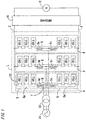
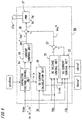
- FIG. 1 is a schematic configuration diagram of a DC power transmission power conversion device according to Embodiment 1 of the present invention.
- the DC power transmission power conversion device of Embodiment 1 includes a power converter 1 as a main circuit, and a control device 20 described later for controlling the power converter 1.
- the power converter 1 performs power conversion between plural-phase AC (here, particularly, three-phase AC) and DC.
- the AC side of the power converter 1 is connected via an interconnection transformer 13 to an AC power supply 14 which is an AC grid, and the DC side is connected via an impedance 15 to a DC power supply 16.
- As the DC power supply 16 in this case, another power conversion device for performing DC output is applied.
- the connection to the AC power supply 14 may be made via an interconnection reactor instead of using the interconnection transformer 13 shown in FIG. 1 .
- each phase of the power converter 1 a positive arm 5 and a negative arm 6 are connected in series.
- An AC end 7 which is the connection point between the positive arm 5 and the negative arm 6 is connected to an AC line for each phase, thus forming a leg circuit 4.
- the leg circuits 4 for three phases are connected in parallel between positive and negative DC buses 2 and 3.
- each leg circuit 4 has cell groups 5a and 6a each including a plurality of converter cells 10 connected in series.
- a positive reactor 9p and a negative reactor 9n are each provided in series between the respective cell groups 5a and 6a and the AC end 7. In this case, the positive reactor 9p, the negative reactor 9n, and the AC end 7 form a reactor 8 having three terminals.
- the locations where the positive reactor 9p and the negative reactor 9n are provided may be any locations in the arms 5 and 6, and a plurality of each reactor may be provided. Their reactor values may be different from each other, or in an extreme case, reactors may be provided only on the positive side or the negative side.
- a transformer is individually provided to each cell group 5a, 6a, the cell groups 5a and 6a are connected in series to each other via primary windings of the transformers, secondary windings of the transformers are connected to each other, and one end of the connected secondary windings is connected to the AC end 7 (see Japanese Laid-Open Patent Publication No. 2013-115837 ).
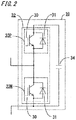
- FIG. 2 shows a configuration example of each converter cell 10.
- the converter cell 10 shown in FIG. 2 is a converter cell 10 in which a half-bridge configuration is employed.
- the converter cell 10 is composed of: a series unit 32 of a plurality of (in this case, two) semiconductor switching elements 30 (hereinafter, simply referred to as switching elements) to which diodes 31 are respectively connected in antiparallel; and a DC capacitor 34 connected in parallel to the series unit 32 and for smoothing DC voltage.
- Each switching element 30 is formed of a self-turn-off switching element such as an IGBT (Insulated Gate Bipolar Transistor) or a GCT (Gate Commutated Turn-off thyristor), and the diodes 31 are respectively connected in antiparallel thereto, to form switches 33P and 33N.
- IGBT Insulated Gate Bipolar Transistor
- GCT Gate Commutated Turn-off thyristor
- both terminals of the switching element 30 of the switch 33N are used as output ends, and through ON/OFF control of the switching elements 30 of the respective switches 33N and 33P, both-end voltage of the DC capacitor 34 and zero voltage are outputted from the output ends.
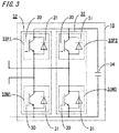
- FIG. 3 shows another configuration example of each converter cell 10.
- the converter cell 10 shown in FIG. 3 is a converter cell 10 in which a full-bridge configuration is employed.
- the converter cell 10 is composed of: two series units 32 connected in parallel; and a DC capacitor 34 connected in parallel to the series units 32 and for smoothing DC voltage.
- Each series unit 32 is composed of a plurality of (in this case, two) switching elements 30 connected in series, to which diodes 31 are respectively connected in antiparallel.
- Each switching element 30 is formed of a self-turn-off switching element such as an IGBT or a GCT, and the diodes 31 are respectively connected in antiparallel thereto, to form switches 33P1, 33P2, 33N1, and 33N2.
- terminals of the switching elements 30 corresponding to the intermediate connection points of the respective series units 32 are used as output ends, and through ON/OFF control of the switching elements 30, positive voltage and negative voltage at both ends of the DC capacitor 34 and zero voltage are outputted from the output ends.
- the converter cell 10 is not limited to the configurations shown in FIG. 2 and FIG. 3 as long as the converter cell 10 is composed of a series unit 32 of a plurality of switching elements 30, and a DC capacitor 34 connected in parallel to the series unit 32, and selectively outputs voltage of the DC capacitor 34 through switching operation.
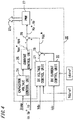
- FIG. 4 is a block diagram showing a configuration example of the control device of the DC power transmission power conversion device according to Embodiment 1 of the present invention.
- Positive arm current ip + and negative arm current ip - flowing through the positive arm 5 and the negative arm 6 for each phase, AC current ip flowing through an AC line for each phase, DC voltage Vdc between the DC buses 2 and 3, DC current idc flowing through the DC buses 2 and 3, capacitor voltage Vcap applied to the DC capacitor 34 in each converter cell 10, are detected by respective detectors (not shown) and then inputted to the control device 20.
- the one calculated from the currents ip + and ip - flowing through the positive arm 5 and the negative arm 6 for each phase may be used.
- the AC current ip for each phase the one calculated from the currents ip + and ip - flowing through the positive arm 5 and the negative arm 6 for each phase may be used.
- a PWM control unit 27 at the next stage generates a gate signal 27a on the basis of the positive arm voltage command Vp + and the negative arm voltage command Vp - , and the operation of each converter cell 10 in the positive arm 5 and the negative arm 6 for each phase is controlled by the gate signal 27a.
- a capacitor voltage control unit 24 in order to control capacitor voltage Vcap of the DC capacitor 34 in each converter cell 10, a capacitor voltage control unit 24 generates, for each phase, an active current command value ipref, a positive arm current command value ip + ref, and a negative arm current command value ip - ref for voltage control for the DC capacitor 34 on the basis of the detected capacitor voltages Vcap of all the converter cells 10 for each phase.
- the current control unit 25 generates, for each phase, voltage commands Vpc + and Vpc - for controlling AC currents flowing through the positive arm 5 and the negative arm 6 for each phase, on the basis of information about the current command values (active current command value ipref, positive arm current command value ip + ref, negative arm current command value ip - ref) given from the capacitor voltage control unit 24, and the positive arm current ip + and the negative arm current ip - detected for each phase and the detected AC current ip for each phase. That is, of the arm voltage commands Vp + and Vp - given to the PWM control unit 27, the voltage commands Vpc + and Vpc - for controlling AC currents flowing through the positive arm 5 and the negative arm 6 for each phase are generated for each phase.
- the DC voltage control unit 21 generates and outputs a main component of a DC voltage command Vdc* for DC voltage control on the basis of the detected DC voltage Vdc between the DC buses 2 and 3, the capacitor voltages Vcap of all the converter cells 10 for each phase, and a DC voltage command value Vdcref as a control target value for DC voltage given from a superior control device (not shown).
- the DC current control unit 22 generates and outputs a partial component (impedance component on DC line) of the DC voltage command Vdc* for DC voltage control on the basis of the detected DC current idc and a DC current command value idcref as a control target value for DC current given from a superior control device (not shown).
- the outputs of the DC voltage control unit 21 and the DC current control unit 22 are added by the adder 23, thereby generating the DC voltage command Vdc* for DC voltage control.
- the voltage commands Vpc + and Vpc - for AC current control for the positive arm 5 and the negative arm 6 for each phase, outputted from the current control unit 25, and the DC voltage command Vdc* obtained by the adder 23, are added by the adder 26, thereby obtaining the positive arm voltage command Vp + and the negative arm voltage command Vp - .
- the PWM control unit 27 generates the gate signal 27a through pulse width modulation control (PWM control) on the basis of the voltage commands Vp + and Vp - , thereby controlling the operation of each converter cell 10.
- the DC voltage control unit 21, the DC current control unit 22, and the adder 23 correspond to a DC control unit in claims.
- Voltage outputted from the cell group 5a in the positive arm 5 and voltage outputted from the cell group 6a in the negative arm 6 include an AC voltage component applied to the AC end 7 of the interconnection transformer 13, a DC voltage component outputted between the DC buses 2 and 3, and a voltage component applied to the positive reactor 9p and the negative reactor 9n.
- a composite voltage ⁇ Vcap obtained by combining (adding or averaging) the capacitor voltages Vcap of all the converter cells 10 composing the power converter 1 is controlled by the operation in which the difference power between active power flowing from the AC power supply 14 and DC power flowing to the DC power supply 16 is converted to DC current flowing to the DC capacitor 34 through switching of each converter cell 10, and the DC capacitor 34 in each converter cell 10 is charged and discharged. Therefore, the composite voltage ⁇ Vcap can be controlled by controlling active current flowing through the AC power supply 14.
- the composite voltage ⁇ Vcap can be controlled through power interchange among the leg circuits 4 for the respective phases. That is, for example, so-called circulating current is caused to flow among the leg circuits 4 for the respective phases to interchange power, whereby imbalance among the phases can be eliminated.
- the capacitor voltage control unit 24 In order to control the capacitor voltage Vcap of the DC capacitor 34 in each converter cell 1 0, the capacitor voltage control unit 24 generates and outputs the active current command value ipref for controlling active current flowing through the AC power supply 14, and the positive arm current command value ip + ref and the negative arm current command value ip - ref for voltage control for the positive arm 5 and the negative arm 6, on the basis of information about the detected capacitor voltage Vcap of each converter cell 10 in each positive arm 5 and each negative arm 6.
- the current control unit 25 controls AC voltage components of voltages outputted from the cell groups 5a and 6a, and voltages applied to the reactors 9p and 9n provided in the positive and negative arms 5 and 6. That is, the current control unit 25 performs feedback control so that the AC current ip for each phase and the detected positive arm current ip + and negative arm current ip - for each phase coincide with the respective current command values (active current command value ipref, positive arm current command value ip + ref, negative arm current command value ip - ref) given from the capacitor voltage control unit 24, thereby generating, for each phase, the voltage commands Vpc + and Vpc - for controlling AC current flowing through the positive arm 5 and the negative arm 6 for each phase.
- the DC voltage control unit 21 performs feedback control so that the detected DC voltage Vdc between the DC buses 2 and 3 coincides with the DC voltage command value Vdcref as a control target value for DC voltage, thereby generating and outputting a main component of the DC voltage command Vdc* for DC voltage control.
- the DC current idc flows when difference voltage between voltage between the DC buses 2 and 3 and voltage of the DC power supply 16 is applied to the impedance 15.
- the DC current control unit 22 performs feedback control so that the detected DC current idc coincides with the DC current command value idcref as a control target value for DC current, thereby generating a partial component (impedance component on DC line) of the DC voltage command Vdc* for controlling DC voltage between the DC buses 2 and 3.
- the outputs of the DC voltage control unit 21 and the DC current control unit 22 are added by the adder 23, thereby calculating the DC voltage command Vdc* for DC voltage control.
- the adder 26 at the next stage adds the voltage commands Vpc + and Vpc for AC current control for the positive arm 5 and the negative arm 6 for each phase outputted from the current control unit 25, and the DC voltage command Vdc* for DC voltage control outputted from the adder 23, thereby calculating the positive arm voltage command Vp + and the negative arm voltage command Vp - .
- the PWM control unit 27 generates the gate signal 27a through pulse width modulation control (PWM control) on the basis of the voltage commands Vp + and Vp - .
- each DC power supply 16 becomes another AC-DC conversion terminal (hereinafter, referred to as a second AC-DC conversion terminal).
- a second AC-DC conversion terminal For example, in the case where the DC power supply 16 as a second AC-DC conversion terminal is provided with the power converter 1 and the control device 20, when the control device 20 as the second AC-DC conversion terminal limits output of the DC current control unit 22 to zero and the DC voltage Vdc between the DC buses 2 and 3 is controlled in accordance with output of the DC voltage control unit 21, the DC power supply 16 as the second AC-DC conversion terminal becomes equivalent to a DC voltage source.
- the control device 20 for the power converter 1 shown in FIG. 4 limits output of the DC current control unit 22 to zero and controls the DC voltage Vdc between the DC buses 2 and 3 in accordance with output of the DC voltage control unit 21, the power converter 1 shown in FIG. 1 performs operation equivalent to a DC voltage source.
- the control device 20 for the power converter 1 shown in FIG. 4 limits output of the DC voltage control unit 21 to zero and controls the DC voltage Vdc between the DC buses 2 and 3 in accordance with output of the DC current control unit 22, thereby performing operation equivalent to a current source, for a DC circuit composed of the impedance 15 and the DC power supply 16.
- control device 20 for the power converter 1 limits output of the DC current control unit 22 to zero and performs control in accordance with output of the DC voltage control unit 21, that is, in the case where the power converter 1 shown in FIG. 1 performs operation equivalent to a DC voltage source, occurrence of grid failure (instantaneous voltage drop) in which the magnitude of AC voltage Vp reduces in the AC power supply 14 will be assumed. In this case, AC power reduces, whereby balance between AC power and DC power is lost, and difference power occurs. In accordance with occurrence of the difference power, the DC capacitor 34 in each converter cell 1 0 is to be charged and discharged.
- the DC voltage control unit 21 on the basis of information about the detected capacitor voltage Vcap of each DC capacitor 34, when the magnitude of the composite voltage ⁇ Vcap obtained by combining (adding or averaging) the capacitor voltages Vcap of all the converter cells 10 for each phase exceeds a first predetermined value ⁇ Vmax set in advance or becomes smaller than a second predetermined value ⁇ Vmin ( ⁇ ⁇ Vmax) set in advance, the DC voltage command value Vdcref is increased or decreased by a fixed value ⁇ Vdcref set in advance, in accordance with the direction of the DC current idc or the DC current command value idcref therefor.
- the first predetermined value ⁇ Vmax is set to be equal to or lower than the overvoltage level of capacitor voltage Vcap, at which failure of the converter cell 10 is detected.
- the second predetermined value ⁇ Vmin is set to be equal to or higher than the low voltage level of the capacitor voltage Vcap, at which failure of the converter cell 1 0 is detected.
- the fixed value ⁇ Vdcref is set in accordance with the magnitude of a resistance component of the impedance 15.
- the DC voltage command value Vdcref is decreased to reduce the amount of the DC current idc flowing out from the power converter 1.
- the DC voltage command value Vdcref is increased to reduce the amount of the DC current idc flowing into the power converter 1.
- the DC voltage command value Vdcref for the DC voltage control unit 21 is controlled in accordance with the variation in the capacitor voltage Vcap, to adjust the magnitude of DC power, whereby AC power and DC power can be balanced even when AC power reduces due to voltage reduction in the AC power supply 14.
- FIG. 5 is a block diagram showing a configuration example of a control device of a DC power transmission power conversion device according to Embodiment 2 of the present invention.
- the configuration of the power converter 1 is the same as that in the above Embodiment 1 shown in FIG. 1 , but the configuration of the control device 20 is different from that in the above Embodiment 1.
- the capacitor voltage control unit 24 in order to control the capacitor voltage Vcap of each converter cell 10, on the basis of information about the detected capacitor voltages Vcap of all the converter cells 10 for each phase, the capacitor voltage control unit 24 generates current command values (active current command value ipref, positive arm current command value ip + ref, negative arm current command value ip - ref) and gives them to the current control unit 25.
- the active current command value ipref outputted from the capacitor voltage control unit 24 is to adjust the active current flowing through the AC power supply 14 in order to perform feedback control of the composite voltage ⁇ Vcap of the capacitor voltages Vcap of all the converter cells 10 for each phase, and the active current command value ipref is constrained by the value of current that can flow in the power converter 1, i.e., the current capacity.
- a limiting value iprefmax is provided so that the active current command value ipref falls within a predetermined range (limiter function).
- the current control unit 25 on the basis of information about the current command values (active current command value ipref, positive arm current command value ip + ref, negative arm current command value ip - ref) given from the capacitor voltage control unit 24, and the detected currents ip, ip + , ip - , the current control unit 25 generates, for each phase, the voltage commands Vpc + and Vpc - for controlling AC current flowing through the positive arm 5 and the negative arm 6, of the arm voltage commands Vp + and Vp - .
- the DC current calculation unit 28 calculates a DC current excessive component ⁇ idc as a DC conversion value of the active current excessive component ⁇ ip, and outputs the DC current excessive component ⁇ idc to the DC current control unit 22.
- the DC voltage control unit 21 does not receive the detection output of the capacitor voltage Vcap of each converter cell 1 0, but receives only information about the DC voltage Vdc between the DC buses 2 and 3. Then, the DC voltage control unit 21 performs feedback control so that the DC voltage Vdc coincides with the DC voltage command value Vdcref as a control target value for DC voltage given from a superior control device (not shown), and generates and outputs a main component of the DC voltage command Vdc* for DC voltage control.
- the DC current control unit 22 generates and outputs a partial component (impedance component on DC line) of the DC voltage command Vdc* for DC voltage control on the basis of information about the detected DC current idc, a DC current command value idcref as a control target value for DC current given from a superior control device (not shown), and the DC current excessive component ⁇ idc given from the DC current calculation unit 28.
- the outputs of the DC voltage control unit 21 and the DC current control unit 22 are added by the adder 23, thereby generating the DC voltage command Vdc* for DC voltage control.
- the voltage components Vpc + and Vpc - for AC current control for the positive arm 5 and the negative arm 6 for each phase, outputted from the current control unit 25, and the DC voltage command Vdc* obtained by the adder 23, are added by the adder 26, thereby obtaining the positive arm voltage command Vp + and the negative arm voltage command Vp - .
- the PWM control unit 27 generates the gate signal 27a through pulse width modulation control (PWM control) on the basis of the voltage commands Vp + and Vp - , thereby controlling the operation of each converter cell 10.
- the limiting value iprefmax is provided so that the active current command value ipref falls within a predetermined range (limiter function). That is, in the feedback control of the composite voltage ⁇ Vcap, a deviation between the composite voltage ⁇ Vcap and a preset command value is amplified to obtain the active current command value ipref, and if the deviation is great, the active current command value ipref is limited by the limiting value iprefmax, whereby a deviation occurs between before and after the limitation.
- the active power excessive amount ⁇ ip in this case may be calculated from a sum of products of the instantaneous-value voltage and current of the three-phase AC, or may be calculated by converting the three-phase AC into an orthogonal coordinate system and similarly calculating a sum of products of the voltage and current.
- the DC current calculation unit 28 calculates an active power excessive amount ⁇ P on the basis of the active current excessive component ⁇ ip outputted from the capacitor voltage control unit 24 and the magnitude of the detected AC voltage Vp. Next, the DC current calculation unit 28 divides the active power excessive amount ⁇ P by the DC voltage Vdc, thereby calculating the DC current excessive component ⁇ idc as a DC conversion value of the active current excessive component ⁇ ip. This calculation is derived from the condition that allows AC power and DC power to be balanced. The DC current excessive component ⁇ idc calculated by the DC current calculation unit 28 is given to the DC current control unit 22.
- the DC current control unit 22 performs the following process on the basis of information about the DC current excessive component ⁇ idc given from the DC current calculation unit 28, the detected DC current idc, and the DC current command value idcref as a control target value for DC current.
- the DC current control unit 22 performs correction to subtract the DC current excessive component ⁇ idc from the DC current command value idcref as a control target value for DC current.
- the DC current control unit 22 performs correction to add the DC current excessive component ⁇ idc to the DC current command value idcref as a control target value for DC current.
- the DC current control unit 22 performs feedback control so that the detected DC current idc coincides with the corrected DC current command value (idcref - ⁇ idc) or (idcref + ⁇ idc), thereby generating and outputting a partial component of the DC voltage command Vdc* so as to control the DC voltage Vdc between the DC buses 2 and 3.
- the DC voltage control unit 21 performs feedback control so that the DC voltage Vdc between the DC buses 2 and 3 coincides with the DC voltage command value Vdcref, thereby generating and outputting a partial component (impedance component on DC line) of the DC voltage command Vdc* for controlling the DC voltage Vdc between the DC buses 2 and 3.
- the adder 23 adds the output of the DC voltage control unit 21 and the output of the DC current control unit 22, thereby calculating the DC voltage command Vdc* for DC voltage control.
- the adder 26 at the next stage adds: the voltage components Vpc + and Vpc - for AC current control for the positive arm 5 and the negative arm 6 for each phase, outputted from the current control unit 25; and the DC voltage command Vdc* for DC voltage control obtained by the adder 23, thereby calculating the positive arm voltage command Vp + and the negative arm voltage command Vp - .
- the PWM control unit 27 generates the gate signal 27a through pulse width modulation control (PWM control) on the basis of the voltage commands Vp + and Vp - .
- PWM control pulse width modulation control
- each DC power supply 16 becomes another AC-DC conversion terminal.
- the DC-interconnected power converters 1 there is at least one AC-DC conversion terminal for controlling the DC voltage Vdc, and the other AC-DC conversion terminals are to control the DC currents idc. The details thereof have been already described in Embodiment 1, so the detailed description is omitted here.
- the capacitor voltage control unit 24 when the capacitor voltage control unit 24 performs feedback control of the composite voltage ⁇ Vcap obtained by combining (adding or averaging) the capacitor voltages of all the converter cells 10, even if the active current command value ipref is limited by the limiter function, the DC current control unit 22 operates so as to correct the DC current command value idcref as a control target value for DC current by the DC current excessive component ⁇ idc.
- the feedback control of the composite voltage ⁇ Vcap is allowed to work.
- the feedback control of the composite voltage ⁇ Vcap works in accordance with the variation in the capacitor voltage Vcap, whereby the capacitor voltage Vcap of the DC capacitor 34 in each converter cell 10 can be stably maintained, and even in the AC-DC conversion terminal that mainly controls the DC current, variation in the capacitor voltage Vcap of each converter cell 10 can be suppressed and the operation can be continued without detecting the failure.
- FIG. 6 is a block diagram showing a configuration example of a control device of a DC power transmission power conversion device according to Embodiment 3 of the present invention.
- the configuration of the power converter 1 is the same as that in the above Embodiment 1 shown in FIG. 1 , but the configuration of the control device 20 is slightly different from those in the above Embodiments 1 and 2.
- the configurations of the DC voltage control unit 21 and the current control unit 25 are the same as those in Embodiment 1, and the configurations of the capacitor voltage control unit 24, the DC current calculation unit 28, the adders 23 and 26, and the PWM control unit 27 are the same as those in Embodiment 2.
- the DC current control unit 22 receives the detected capacitor voltages Vcap of all the converter cells 10 for each phase. On the basis of the above information, the DC current control unit 22 outputs a partial component (impedance component on DC line) of the DC voltage command Vdc*.
- the DC current control unit 22 on the basis of information about the detected capacitor voltage Vcap of each DC capacitor 34, when the magnitude of the composite voltage ⁇ Vcap obtained by combining (adding or averaging) the capacitor voltages of all the converter cells 10 for each phase exceeds a first predetermined value ⁇ Vmax set in advance or becomes smaller than a second predetermined value ⁇ Vmin ( ⁇ ⁇ Vmax) set in advance, the function of limiting the DC current control unit 22 to cause its output to be zero is released to allow the feedback control in the DC current control unit 22 to work.
- the DC current control unit 22 performs correction to subtract or add the DC current excessive component ⁇ idc from or to the DC current command value idcref as a control target value for DC current, in accordance with the case where the DC current idc has such a polarity that indicates power flowing from the power converter 1 to the DC power supply 16, or the case where the DC current idc has such a polarity that indicates power flowing from the DC power supply 16 to the power converter 1.
- the DC current control unit 22 performs feedback control so that the detected DC current idc coincides with the corrected DC current command value (idcref - ⁇ idc) or (idcref + ⁇ idc), thereby generating and outputting a partial component of the DC voltage command Vdc* so as to control the DC voltage Vdc between the DC buses 2 and 3.
- the DC voltage command value Vdcref of the DC voltage control unit 21 is controlled to decrease the magnitude of DC power as in Embodiment 1, and in addition, in the DC current control unit 22, the DC current command value idcref as a control target value for DC current is corrected by the DC current excessive component ⁇ idc.
- the present invention is not limited to only the configurations in the above Embodiments 1 to 3. Without deviating from the present invention, the configurations in the above Embodiments 1 to 3 may be partially modified or partially omitted, and further, the configurations in the above Embodiments 1 to 3 may be combined with each other as appropriate.
Landscapes
- Engineering & Computer Science (AREA)
- Power Engineering (AREA)
- Inverter Devices (AREA)
- Rectifiers (AREA)
Claims (9)
- Dispositif de conversion de puissance pour transmission de puissance en courant continu CC, comprenant :- un convertisseur de puissance (1) incluant des barres omnibus CC positive et négative (2, 3) et une pluralité de circuits ramifiés (4) composés d'une branche positive (5) et d'une branche négative (6) pour chaque phase qui sont connectés en série les uns avec les autres et comportent un point de connexion entre eux, susceptibles d'être connectés à une ligne à courant alternatif CA pour une phase correspondante, les circuits ramifiés (4) étant connectés en parallèle entre les barres omnibus CC positive et négative (2, 3),
le convertisseur de puissance (1) étant configuré pour effectuer une conversion de puissance entre un courant alternatif CA à plusieurs phases et un courant continu ; et- un dispositif de commande (20) configuré pour commander le convertisseur de puissance (1),dans lequel chacune de la branche positive (5) et de la branche négative (6) composant chaque circuit ramifié (4) est composée d'au moins une cellule de conversion (10) connectée en série,
la cellule de conversion (10) est composée d'une unité en série (32) d'une pluralité d'éléments de commutation à semi-conducteurs (30) connectés en série, et un condensateur à CC (34) connecté en parallèle à l'unité en série (32),
le dispositif de commande (20) est configuré pour effectuer une commande de sortie pour chaque cellule de conversion (10) composant la branche positive (5) et la branche négative (6),
le dispositif de commande (20) inclut :- une unité de commande de tension de condensateur (24) configurée pour générer une valeur d'ordre de courant (ipref, ip*ref, ip'ref) pour une commande de tension sur la base d'une information concernant la tension de condensateur détectée (Vcap) de chaque cellule de conversion (10) dans chaque branche positive (5) et chaque branche négative (6) ;- une unité de commande de courant (25) configurée pour, sur la base de la valeur d'ordre de courant (ipref, ip*ref, ip'ref) provenant de l'unité de commande de tension de condensateur (24), générer un ordre de tension (Vpc+, Vpc-) pour une commande de courant CA, d'un ordre de tension de branche positive (Vp+) pour commander un courant qui s'écoule à travers la branche positive (5) et d'un ordre de tension de branche négative (Vp-) pour commander un courant qui s'écoule à travers la branche négative (6) ; et- une unité de commande CC (21, 22, 23) configurée pour, sur la base d'une tension CC (Vdc) entre les barres omnibus CC, du courant CC (idc) qui s'écoule à travers les barres omnibus CC, et d'une valeur d'ordre (Vdcref, idcref) comprenant au moins une valeur parmi une valeur d'ordre de tension CC (Vdcref) et une valeur d'ordre de courant CC (idcref) à titre de valeur cible de commande préétablie, générer un ordre de tension CC (Vdc*) pour une commande de tension CC, de l'ordre de tension de branche positive (Vp+) et de l'ordre de tension de branche négative (Vp-), l'ordre de tension de branche positive (Vp+) et l'ordre de tension de branche négative (Vp-) qui sont générés en ajoutant l'ordre de tension CC (Vdc*) aux ordres de tension d'une branche positive (Vpc+) et d'une branche négative (Vpc-) respectivement, et les cellules de conversion étant agencées de manière à être commandées sur la base de l'ordre de tension de branche positive (Vp+) et de l'ordre de tension de branche négative (Vp-), dans lequel le dispositif de commande (20) est configuré pour :
augmenter ou diminuer, en accord avec la direction du courant CC ou avec la valeur d'ordre de courant CC, la valeur d'ordre de tension CC (Vdcref) à fournir à l'unité de commande CC (21, 22, 23) à raison d'une valeur prédéterminée fixe quand une tension composite (SVcap), obtenue en combinant, c'est-à-dire en additionnant ou en moyennant, les tensions de condensateur (Vcap) de toutes les cellules de conversion (10), excède une première valeur prédéterminée ou devient plus petite qu'une seconde valeur prédéterminée, et/ou corriger la valeur d'ordre de courant CC (idcref) à fournir à l'unité de commande CC (21, 22, 23) sur la base d'une composante excessive de courant CC (Didc) obtenue par calcul en utilisant une quantité en excès (Dip) par rapport à une valeur de limitation (iprefmax) pour la valeur d'ordre de courant, fournie de telle façon que la valeur d'ordre de courant active (ipref) tombe à l'intérieur d'une plage prédéterminée, la tension CA (Vp) pour chaque phase et la tension CC (Vdc). - Dispositif de conversion de puissance pour transmission de puissance CC selon la revendication 1,
dans lequel l'unité de commande CC (21, 22, 23) inclut une unité de commande de tension CC (21) configurée pour générer une composante principale de l'ordre de tension CC (Vdc*) sur la base de la tension (Vdc) entre les barres omnibus CC, de la tension composite (SVcap) des condensateurs CC, et de la valeur d'ordre de tension CC (Vdcref), la variation de tension dans chaque condensateur CC (34) étant détectée sur la base du fait que la tension composite (SVcap) des condensateurs CC (34) excède la première valeur prédéterminée (DVmax) fixée à l'avance ou devient plus petite que la deuxième valeur prédéterminée (DVmin) fixée pour être plus petite que la première valeur prédéterminée (DVmax), et
en réponse à la détection, corriger la valeur d'ordre de tension CC (Vdcref) fixée par l'unité de commande de tension CC (21) en ajoutant à celle-ci ou en soustrayant de celle-ci la valeur fixée préétablie (DVdcref) en accord avec la polarité du courant CC (idc) ou avec la valeur d'ordre (idcref) pour la commande de courant CC. - Dispositif de conversion de puissance pour transmission de puissance CC selon la revendication 1, dans lequel l'unité de commande CC (21, 22, 23) inclut une unité de commande de courant CC (22) pour générer une composante partielle de l'ordre de tension CC (Vdc*) sur la base du courant CC (idc) qui s'écoule à travers les barres omnibus CC et la valeur d'ordre de courant CC,
le dispositif de commande (20) est configuré de telle manière qu'une variation de tension dans chaque condensateur CC (34) est détectée sur la base du fait que la valeur d'ordre de courant (ipref) générée par l'unité de commande de tension de condensateur (24) excède la valeur de limitation (iprefmax) fixée à l'avance pour l'unité de commande de tension de condensateur (24), et en réponse à la détection, la valeur d'ordre de courant CC (idcref) fixée pour l'unité de commande de courant CC est corrigée sur la base de la composante en excès de courant CC (Didc) obtenue par calcul en utilisant la quantité en excès (Dip) par rapport à la valeur de limitation (iprefmax) pour la valeur d'ordre de courant, la tension CA (Vp) pour chaque phase, et la tension CC (Vdc). - Dispositif de conversion de puissance pour transmission de puissance CC selon la revendication 1, dans lequel l'unité de commande CC (21, 22, 23) inclut une unité de commande de tension CC (21) pour générer une composante principale de l'ordre de tension CC (Vdc*) sur la base de la tension (Vdc) entre les barres omnibus CC, de la tension composite (SVcap) des condensateurs CC (34), et de la valeur d'ordre de tension CC (Vdcref) ; et une unité de commande de courant CC (22) pour générer une composante partielle de l'ordre de tension CC (Vdc*) sur la base du courant CC (idc) qui s'écoule à travers les barres omnibus CC et de la valeur d'ordre de courant CC (idcref),
la variation de tension dans chaque condensateur CC (34) étant détectée sur la base du fait que la tension composite (SVcap) des condensateurs CC (34) excède la première valeur prédéterminée (DVmax) fixée à l'avance ou devient plus petite que la deuxième valeur prédéterminée (DVmin) fixée pour être plus petite que la première valeur prédéterminée (DVmax), et
en réponse à la détection, la valeur d'ordre de tension CC (Vdcref) fixée pour l'unité de commande de tension CC (21) est corrigée en ajoutant à celle-ci ou en soustrayant de celle-ci la valeur fixée préétablie (DVdcref) en accord avec la polarité du courant CC (idc) ou la valeur d'ordre de courant CC (idcref) pour la commande de courant CC, et la valeur d'ordre de courant CC (idcref) fixée pour l'unité de commande de courant CC (22) est corrigée sur la base de la composante en excès du courant CC (Didc) obtenue par calcul en utilisant la quantité en excès (Dip) par rapport à la valeur de limitation (iprefmax) pour la valeur d'ordre de courant, la tension CA (Vp) pour chaque phase, et la tension CC (Vdc). - Dispositif de conversion de puissance pour transmission de puissance CC selon la revendication 2 ou 4,
dans lequel le dispositif de commande (20) est configuré de telle façon que lorsqu'il a détecté que la tension composite (SVcap) des condensateurs CC (34) n'est pas supérieure à la première valeur prédéterminée (DVmax) et n'est pas plus petite que la seconde valeur prédéterminée (DVmin), la correction pour la valeur d'ordre de tension CC (Vdcref) dans l'unité de commande de tension CC (21) est arrêtée. - Dispositif de conversion de puissance pour transmission de puissance CC selon la revendication 3 ou 4,
dans lequel le dispositif de commande (20) est configuré de telle façon que lorsqu'il a détecté que l'intensité du courant CC (idc) n'est pas supérieure à une valeur prédéterminée, la correction pour la valeur d'ordre de courant CC (idcref) dans l'unité de commande de courant CC (22) est arrêtée. - Dispositif de conversion de puissance pour transmission de puissance CC selon la revendication 5,
dans lequel le dispositif de commande (20) est configuré de telle façon que l'arrêt de la correction pour la valeur d'ordre de tension CC (Vdcref) dans l'unité de commande de tension CC est exécuté de manière telle que la valeur d'ordre corrigée est progressivement changée vers la valeur d'ordre avant la correction. - Dispositif de conversion de puissance pour transmission de puissance CC selon la revendication 6,
dans lequel le dispositif de commande (20) est configuré de telle façon que l'arrêt de la correction pour la valeur d'ordre de courant CC (idcref) dans l'unité de commande de courant CC (22) est exécuté de manière telle que la composante de tension CC (Vdc*) de l'ordre de tension de branche positive (Vp+) et de l'ordre de tension de branche négative (Vp -) est progressivement changée. - Procédé de conversion de puissance pour transmission de puissance CC, dans lequel il est prévu un convertisseur de puissance (1) qui inclut une pluralité de circuits ramifiés (4) composés d'une branche positive (5) et d'une branche négative (6) pour chaque phase, qui sont connectés en série les uns aux autres et qui ont un point de connexion (7) entre eux, connectés à une ligne CA pour une phase correspondante, les circuits ramifiés (4) étant connectés en parallèle entre des barres omnibus CC positive et négative (2, 3), le convertisseur de puissance (1) effectuant une conversion de puissance entre une pluralité de phases CA et un courant continu CC, et
un dispositif de commande (20) pour commander le convertisseur de puissance (1),
dans lequel chacune de la branche positive (5) et de la branche négative (6) qui composent chaque circuit ramifié (4) est composée d'au moins une cellule de conversion (10) connectée en série, la cellule de conversion (10) étant composée d'une unité en série (32) d'une pluralité d'éléments de commutation à semi-conducteurs (30) connectés en série, et d'un condensateur CC (34) connecté en parallèle à l'unité en série (32),
dans lequel le procédé comprend les étapes, mises en œuvre par le dispositif de commande (20), lorsqu'il effectue la commande de sortie pour chaque cellule de conversion (10) composant la branche positive (5) et la branche négative (6),
consistant à :générer une valeur d'ordre de courant (ipref, ip*ref, ip'ref) sur la base d'une information concernant la tension de condensateur détectée (Vcap) de chaque cellule de conversion (10) dans chaque branche positive (5) et chaque branche négative (6) ;générer, sur la base de la valeur d'ordre de courant (ipref, ip*ref, ip'ref), une valeur d'ordre (Vpc+, Vpc-) pour la commande de courant CA, d'un ordre de tension de branche positive (Vp+) pour commander le courant qui s'écoule à travers la branche positive (5), et d'un ordre de tension de branche négative (Vp-) pour commander le courant qui s'écoule à travers la branche négative (6), générer, sur la base d'une tension CC (Vdc) entre les barres omnibus CC, du courant CC (idc) qui s'écoule à travers les barres omnibus CC, et d'une valeur d'ordre (Vdcref, idcref) comprenant au moins une valeur parmi une valeur d'ordre de tension CC (Vdcref) et une valeur d'ordre de courant CC (idcref) à titre de valeur cible de commande préétablie, un ordre de tension CC (Vdc*) pour la commande de tension CC, de l'ordre de tension de branche positive (Vp+) et de l'ordre de tension de branche négative (Vp-), l'ordre de tension de branche positive (Vp+) et l'ordre de tension de branche négative (Vp-) étant générés en ajoutant l'ordre de tension CC (Vdc*) aux ordres de tension d'une branche positive (Vpc+) et d'une branche négative (Vpc-) respectivement, et les cellules de conversion étant commandées sur la base de l'ordre de tension de branche positive (Vp+) et de l'ordre de tension de branche négative (Vp-), etaugmenter ou diminuer, en accord avec la direction du courant CC ou la valeur d'ordre de courant CC, la valeur d'ordre de tension CC (Vdcref) à fournir à l'unité de commande CC (21, 22, 23), à raison d'une valeur prédéterminée fixe quand une tension composite (SVcap) obtenue en combinant, c'est-à-dire en ajoutant ou en moyennant, les tensions de condensateur (Vcap) de toutes les cellules de conversion (10), excède une première valeur prédéterminée ou devient plus petite qu'une deuxième valeur prédéterminée, et/oucorriger la valeur d'ordre de courant CC (idcref) à fournir à l'unité de commande CC (21, 22, 23) sur la base d'une composante en excès du courant CC (Didc) obtenue par calcul en utilisant une quantité en excès (Dip) par rapport à une valeur de limitation (iprefmax) pour la valeur d'ordre de courant, prévue de telle façon que la valeur d'ordre de courante active (ipref) tombe à l'intérieur d'une plage prédéterminée, la tension CA (Vp) pour chaque phase, et la tension CC (Vdc).
Applications Claiming Priority (2)
| Application Number | Priority Date | Filing Date | Title |
|---|---|---|---|
| JP2014104869 | 2014-05-21 | ||
| PCT/JP2015/064327 WO2015178376A1 (fr) | 2014-05-21 | 2015-05-19 | Dispositif et procédé de conversion de puissance pour transmission de puissance de courant continu |
Publications (3)
| Publication Number | Publication Date |
|---|---|
| EP3148067A1 EP3148067A1 (fr) | 2017-03-29 |
| EP3148067A4 EP3148067A4 (fr) | 2018-01-24 |
| EP3148067B1 true EP3148067B1 (fr) | 2020-10-07 |
Family
ID=54554044
Family Applications (1)
| Application Number | Title | Priority Date | Filing Date |
|---|---|---|---|
| EP15795713.5A Active EP3148067B1 (fr) | 2014-05-21 | 2015-05-19 | Dispositif et procédé de conversion de puissance pour transmission de puissance de courant continu |
Country Status (4)
| Country | Link |
|---|---|
| US (1) | US9755542B2 (fr) |
| EP (1) | EP3148067B1 (fr) |
| JP (1) | JP6207730B2 (fr) |
| WO (1) | WO2015178376A1 (fr) |
Families Citing this family (32)
| Publication number | Priority date | Publication date | Assignee | Title |
|---|---|---|---|---|
| WO2015104922A1 (fr) * | 2014-01-09 | 2015-07-16 | 三菱電機株式会社 | Système de conversion électrique |
| JP6180641B2 (ja) * | 2014-08-01 | 2017-08-16 | 三菱電機株式会社 | 電力変換装置 |
| JP6227192B2 (ja) * | 2015-03-17 | 2017-11-08 | 三菱電機株式会社 | 電力変換装置 |
| JP6509352B2 (ja) * | 2015-09-17 | 2019-05-08 | 三菱電機株式会社 | 電力変換装置 |
| JP6522141B2 (ja) * | 2015-09-17 | 2019-05-29 | 三菱電機株式会社 | 電力変換装置 |
| EP3352360B9 (fr) * | 2015-09-17 | 2024-07-03 | Mitsubishi Electric Corporation | Dispositif de conversion de puissance |
| CN209447712U (zh) * | 2015-12-14 | 2019-09-27 | 西门子股份公司 | 交流断路器 |
| JP6818414B2 (ja) * | 2016-02-09 | 2021-01-20 | 北海道電力株式会社 | 電力変換装置の制御システムおよび制御方法 |
| JP6618823B2 (ja) * | 2016-02-09 | 2019-12-11 | 株式会社東芝 | 電力変換装置 |
| JP6612639B2 (ja) * | 2016-02-09 | 2019-11-27 | 株式会社東芝 | 電力変換器の制御装置 |
| JP6549049B2 (ja) * | 2016-02-09 | 2019-07-24 | 株式会社東芝 | 電力変換器の制御装置 |
| US10931113B2 (en) | 2016-03-15 | 2021-02-23 | Mitsubishi Electric Corporation | Power conversion device and power system performing protection control for suppressing received power |
| US10673352B2 (en) * | 2016-03-28 | 2020-06-02 | Mitsubishi Electric Corporation | Power conversion apparatus comprising cell blocks each including cascaded converter cells and a bypass circuit connected thereto |
| JP6541155B2 (ja) * | 2016-06-27 | 2019-07-10 | 東芝三菱電機産業システム株式会社 | 電力変換装置及びその制御方法 |
| FR3053854B1 (fr) * | 2016-07-05 | 2018-08-17 | Supergrid Institute | Module de controle de l'energie interne d'un convertisseur |
| JP6690880B2 (ja) * | 2016-12-06 | 2020-04-28 | 東芝三菱電機産業システム株式会社 | 電力変換装置 |
| JP6719401B2 (ja) * | 2017-02-17 | 2020-07-08 | 株式会社東芝 | 電力変換装置 |
| WO2018158935A1 (fr) * | 2017-03-03 | 2018-09-07 | 三菱電機株式会社 | Dispositif de conversion de courant et procédé de communication |
| WO2018229857A1 (fr) * | 2017-06-13 | 2018-12-20 | 三菱電機株式会社 | Systeme convertisseur de courant |
| FR3068842B1 (fr) * | 2017-07-07 | 2022-03-04 | Inst Supergrid | Convertisseur muni d'un module de gestion de l'energie en partie alternative |
| CN107612290B (zh) * | 2017-09-25 | 2019-12-31 | 南方电网科学研究院有限责任公司 | 换流器的电容电压排序频率的优化控制方法和系统 |
| CN107994599B (zh) * | 2017-12-07 | 2020-10-16 | 南京南瑞继保电气有限公司 | 一种串联式电压源换流阀组的协调控制方法及装置 |
| US11444552B2 (en) * | 2019-03-29 | 2022-09-13 | Tohoku University | Electric power converting device, and electricity generating system |
| WO2020240810A1 (fr) * | 2019-05-31 | 2020-12-03 | 東芝エネルギーシステムズ株式会社 | Dispositif de conversion de puissance |
| CN110504688B (zh) * | 2019-08-12 | 2020-12-29 | 上海交通大学 | 具备交直流故障不间断运行能力的固态变压器及控制方法 |
| WO2021176614A1 (fr) * | 2020-03-04 | 2021-09-10 | 三菱電機株式会社 | Dispositif de conversion de puissance |
| WO2021181583A1 (fr) * | 2020-03-11 | 2021-09-16 | 三菱電機株式会社 | Dispositif de conversion de puissance |
| EP4131766A4 (fr) | 2020-03-30 | 2023-05-03 | Mitsubishi Electric Corporation | Dispositif de conversion d'énergie |
| CN113765426B (zh) * | 2020-06-01 | 2024-08-20 | 台达电子企业管理(上海)有限公司 | 模块化多电平换流器的控制方法及控制系统与输电系统 |
| US12289063B2 (en) | 2020-09-18 | 2025-04-29 | Hitachi Mitsubishi Hydro Corporation | Modular multilevel power converter and variable speed generator-motor |
| US12438476B2 (en) * | 2021-03-31 | 2025-10-07 | Mitsubishi Electric Corporation | Power conversion device |
| JPWO2024154308A1 (fr) * | 2023-01-19 | 2024-07-25 |
Family Cites Families (14)
| Publication number | Priority date | Publication date | Assignee | Title |
|---|---|---|---|---|
| JP2635660B2 (ja) * | 1988-03-16 | 1997-07-30 | 東京電力株式会社 | 系統直流連系装置の制御装置 |
| CA1313219C (fr) * | 1988-10-07 | 1993-01-26 | Boon-Teck Ooi | Systeme de transmission a courant continu haute tension a modulation d'impulsions en duree et convertisseur |
| US7599196B2 (en) * | 2006-06-06 | 2009-10-06 | Ideal Power Converters, Inc. | Universal power converter |
| CN101606309B (zh) * | 2007-02-16 | 2013-02-27 | 株式会社小松制作所 | 电压控制装置及电压控制方法 |
| AU2008350481B2 (en) * | 2008-02-13 | 2012-09-13 | Mitsubishi Electric Corporation | Power converting device |
| US8704498B2 (en) * | 2009-06-15 | 2014-04-22 | Alstom Technology Ltd. | Converter |
| JP4969614B2 (ja) * | 2009-07-21 | 2012-07-04 | 株式会社日立製作所 | 電力変換装置 |
| JP5455055B2 (ja) | 2010-02-26 | 2014-03-26 | 国立大学法人東京工業大学 | 電力変換器 |
| JP5721096B2 (ja) * | 2010-08-23 | 2015-05-20 | 国立大学法人東京工業大学 | 電力変換器 |
| CN102215004B (zh) * | 2011-03-16 | 2014-07-30 | 中国电力科学研究院 | 一种基于模块化多电平换流器的阀电流控制方法 |
| JP5941631B2 (ja) * | 2011-07-26 | 2016-06-29 | 株式会社日立製作所 | 電力変換装置 |
| JP5827924B2 (ja) * | 2012-05-30 | 2015-12-02 | 株式会社日立製作所 | 電圧型電力変換装置の制御装置及び制御方法 |
| WO2014162620A1 (fr) | 2013-04-02 | 2014-10-09 | 三菱電機株式会社 | Dispositif de conversion de puissance |
| WO2015104922A1 (fr) | 2014-01-09 | 2015-07-16 | 三菱電機株式会社 | Système de conversion électrique |
-
2015
- 2015-05-19 EP EP15795713.5A patent/EP3148067B1/fr active Active
- 2015-05-19 JP JP2016521106A patent/JP6207730B2/ja active Active
- 2015-05-19 WO PCT/JP2015/064327 patent/WO2015178376A1/fr not_active Ceased
- 2015-05-19 US US15/305,586 patent/US9755542B2/en active Active
Non-Patent Citations (1)
| Title |
|---|
| None * |
Also Published As
| Publication number | Publication date |
|---|---|
| JPWO2015178376A1 (ja) | 2017-04-20 |
| JP6207730B2 (ja) | 2017-10-04 |
| US9755542B2 (en) | 2017-09-05 |
| EP3148067A4 (fr) | 2018-01-24 |
| US20170047860A1 (en) | 2017-02-16 |
| EP3148067A1 (fr) | 2017-03-29 |
| WO2015178376A1 (fr) | 2015-11-26 |
Similar Documents
| Publication | Publication Date | Title |
|---|---|---|
| EP3148067B1 (fr) | Dispositif et procédé de conversion de puissance pour transmission de puissance de courant continu | |
| EP3273586B1 (fr) | Dispositif de conversion de puissance | |
| US10826378B2 (en) | Power conversion apparatus for interconnection with a three-phrase ac power supply | |
| JP6509352B2 (ja) | 電力変換装置 | |
| US10326355B2 (en) | Power conversion device | |
| EP3093975B1 (fr) | Système de conversion électrique | |
| US10560036B2 (en) | Power conversion device for reliable control of circulating current while maintaining voltage of a cell | |
| JP6591064B2 (ja) | 電力変換システム | |
| US12057787B2 (en) | Power conversion device | |
| EP3432459A1 (fr) | Dispositif de conversion d'énergie et système d'alimentation | |
| US12413156B2 (en) | Capacitor balancing control in an HVDC MMC | |
| US12273045B2 (en) | Power conversion device with individual cell and arm balancing | |
| EP3093976A1 (fr) | Système de conversion d'énergie électrique | |
| JPWO2019215842A1 (ja) | 電力変換装置 | |
| JP2018129963A (ja) | 電力変換器の制御装置 | |
| US12255544B2 (en) | Power conversion device that performs power conversion between DC circuit and AC circuit | |
| JP5904883B2 (ja) | 変圧器多重電力変換装置 | |
| JP7371545B2 (ja) | 電力変換装置およびその制御方法 | |
| EP4521624A1 (fr) | Dispositif de conversion de puissance | |
| JP2022165495A (ja) | 電力変換装置 | |
| JP2025088984A (ja) | 電力変換システム及び制御方法 |
Legal Events
| Date | Code | Title | Description |
|---|---|---|---|
| STAA | Information on the status of an ep patent application or granted ep patent |
Free format text: STATUS: THE INTERNATIONAL PUBLICATION HAS BEEN MADE |
|
| PUAI | Public reference made under article 153(3) epc to a published international application that has entered the european phase |
Free format text: ORIGINAL CODE: 0009012 |
|
| STAA | Information on the status of an ep patent application or granted ep patent |
Free format text: STATUS: REQUEST FOR EXAMINATION WAS MADE |
|
| 17P | Request for examination filed |
Effective date: 20161026 |
|
| AK | Designated contracting states |
Kind code of ref document: A1 Designated state(s): AL AT BE BG CH CY CZ DE DK EE ES FI FR GB GR HR HU IE IS IT LI LT LU LV MC MK MT NL NO PL PT RO RS SE SI SK SM TR |
|
| AX | Request for extension of the european patent |
Extension state: BA ME |
|
| DAV | Request for validation of the european patent (deleted) | ||
| DAX | Request for extension of the european patent (deleted) | ||
| A4 | Supplementary search report drawn up and despatched |
Effective date: 20171221 |
|
| RIC1 | Information provided on ipc code assigned before grant |
Ipc: H02M 7/483 20070101AFI20171215BHEP Ipc: H02M 7/48 20070101ALI20171215BHEP Ipc: H02M 1/00 20060101ALN20171215BHEP Ipc: H02M 1/32 20070101ALN20171215BHEP Ipc: H02M 7/12 20060101ALI20171215BHEP |
|
| STAA | Information on the status of an ep patent application or granted ep patent |
Free format text: STATUS: EXAMINATION IS IN PROGRESS |
|
| 17Q | First examination report despatched |
Effective date: 20190814 |
|
| GRAP | Despatch of communication of intention to grant a patent |
Free format text: ORIGINAL CODE: EPIDOSNIGR1 |
|
| STAA | Information on the status of an ep patent application or granted ep patent |
Free format text: STATUS: GRANT OF PATENT IS INTENDED |
|
| RIC1 | Information provided on ipc code assigned before grant |
Ipc: H02M 7/483 20070101AFI20200331BHEP Ipc: H02M 1/32 20070101ALN20200331BHEP Ipc: H02M 7/12 20060101ALI20200331BHEP Ipc: H02M 7/48 20070101ALI20200331BHEP Ipc: H02M 1/00 20060101ALN20200331BHEP |
|
| INTG | Intention to grant announced |
Effective date: 20200417 |
|
| GRAS | Grant fee paid |
Free format text: ORIGINAL CODE: EPIDOSNIGR3 |
|
| GRAA | (expected) grant |
Free format text: ORIGINAL CODE: 0009210 |
|
| STAA | Information on the status of an ep patent application or granted ep patent |
Free format text: STATUS: THE PATENT HAS BEEN GRANTED |
|
| AK | Designated contracting states |
Kind code of ref document: B1 Designated state(s): AL AT BE BG CH CY CZ DE DK EE ES FI FR GB GR HR HU IE IS IT LI LT LU LV MC MK MT NL NO PL PT RO RS SE SI SK SM TR |
|
| REG | Reference to a national code |
Ref country code: GB Ref legal event code: FG4D |
|
| REG | Reference to a national code |
Ref country code: CH Ref legal event code: EP Ref country code: AT Ref legal event code: REF Ref document number: 1322231 Country of ref document: AT Kind code of ref document: T Effective date: 20201015 |
|
| REG | Reference to a national code |
Ref country code: DE Ref legal event code: R096 Ref document number: 602015060209 Country of ref document: DE |
|
| REG | Reference to a national code |
Ref country code: IE Ref legal event code: FG4D |
|
| REG | Reference to a national code |
Ref country code: SE Ref legal event code: TRGR |
|
| REG | Reference to a national code |
Ref country code: NL Ref legal event code: MP Effective date: 20201007 |
|
| REG | Reference to a national code |
Ref country code: AT Ref legal event code: MK05 Ref document number: 1322231 Country of ref document: AT Kind code of ref document: T Effective date: 20201007 |
|
| PG25 | Lapsed in a contracting state [announced via postgrant information from national office to epo] |
Ref country code: FI Free format text: LAPSE BECAUSE OF FAILURE TO SUBMIT A TRANSLATION OF THE DESCRIPTION OR TO PAY THE FEE WITHIN THE PRESCRIBED TIME-LIMIT Effective date: 20201007 Ref country code: RS Free format text: LAPSE BECAUSE OF FAILURE TO SUBMIT A TRANSLATION OF THE DESCRIPTION OR TO PAY THE FEE WITHIN THE PRESCRIBED TIME-LIMIT Effective date: 20201007 Ref country code: PT Free format text: LAPSE BECAUSE OF FAILURE TO SUBMIT A TRANSLATION OF THE DESCRIPTION OR TO PAY THE FEE WITHIN THE PRESCRIBED TIME-LIMIT Effective date: 20210208 Ref country code: NL Free format text: LAPSE BECAUSE OF FAILURE TO SUBMIT A TRANSLATION OF THE DESCRIPTION OR TO PAY THE FEE WITHIN THE PRESCRIBED TIME-LIMIT Effective date: 20201007 Ref country code: NO Free format text: LAPSE BECAUSE OF FAILURE TO SUBMIT A TRANSLATION OF THE DESCRIPTION OR TO PAY THE FEE WITHIN THE PRESCRIBED TIME-LIMIT Effective date: 20210107 Ref country code: GR Free format text: LAPSE BECAUSE OF FAILURE TO SUBMIT A TRANSLATION OF THE DESCRIPTION OR TO PAY THE FEE WITHIN THE PRESCRIBED TIME-LIMIT Effective date: 20210108 |
|
| REG | Reference to a national code |
Ref country code: LT Ref legal event code: MG4D |
|
| PG25 | Lapsed in a contracting state [announced via postgrant information from national office to epo] |
Ref country code: ES Free format text: LAPSE BECAUSE OF FAILURE TO SUBMIT A TRANSLATION OF THE DESCRIPTION OR TO PAY THE FEE WITHIN THE PRESCRIBED TIME-LIMIT Effective date: 20201007 Ref country code: AT Free format text: LAPSE BECAUSE OF FAILURE TO SUBMIT A TRANSLATION OF THE DESCRIPTION OR TO PAY THE FEE WITHIN THE PRESCRIBED TIME-LIMIT Effective date: 20201007 Ref country code: BG Free format text: LAPSE BECAUSE OF FAILURE TO SUBMIT A TRANSLATION OF THE DESCRIPTION OR TO PAY THE FEE WITHIN THE PRESCRIBED TIME-LIMIT Effective date: 20210107 Ref country code: LV Free format text: LAPSE BECAUSE OF FAILURE TO SUBMIT A TRANSLATION OF THE DESCRIPTION OR TO PAY THE FEE WITHIN THE PRESCRIBED TIME-LIMIT Effective date: 20201007 Ref country code: PL Free format text: LAPSE BECAUSE OF FAILURE TO SUBMIT A TRANSLATION OF THE DESCRIPTION OR TO PAY THE FEE WITHIN THE PRESCRIBED TIME-LIMIT Effective date: 20201007 Ref country code: IS Free format text: LAPSE BECAUSE OF FAILURE TO SUBMIT A TRANSLATION OF THE DESCRIPTION OR TO PAY THE FEE WITHIN THE PRESCRIBED TIME-LIMIT Effective date: 20210207 |
|
| PG25 | Lapsed in a contracting state [announced via postgrant information from national office to epo] |
Ref country code: HR Free format text: LAPSE BECAUSE OF FAILURE TO SUBMIT A TRANSLATION OF THE DESCRIPTION OR TO PAY THE FEE WITHIN THE PRESCRIBED TIME-LIMIT Effective date: 20201007 |
|
| REG | Reference to a national code |
Ref country code: DE Ref legal event code: R097 Ref document number: 602015060209 Country of ref document: DE |
|
| PG25 | Lapsed in a contracting state [announced via postgrant information from national office to epo] |
Ref country code: EE Free format text: LAPSE BECAUSE OF FAILURE TO SUBMIT A TRANSLATION OF THE DESCRIPTION OR TO PAY THE FEE WITHIN THE PRESCRIBED TIME-LIMIT Effective date: 20201007 Ref country code: CZ Free format text: LAPSE BECAUSE OF FAILURE TO SUBMIT A TRANSLATION OF THE DESCRIPTION OR TO PAY THE FEE WITHIN THE PRESCRIBED TIME-LIMIT Effective date: 20201007 Ref country code: SM Free format text: LAPSE BECAUSE OF FAILURE TO SUBMIT A TRANSLATION OF THE DESCRIPTION OR TO PAY THE FEE WITHIN THE PRESCRIBED TIME-LIMIT Effective date: 20201007 Ref country code: LT Free format text: LAPSE BECAUSE OF FAILURE TO SUBMIT A TRANSLATION OF THE DESCRIPTION OR TO PAY THE FEE WITHIN THE PRESCRIBED TIME-LIMIT Effective date: 20201007 Ref country code: RO Free format text: LAPSE BECAUSE OF FAILURE TO SUBMIT A TRANSLATION OF THE DESCRIPTION OR TO PAY THE FEE WITHIN THE PRESCRIBED TIME-LIMIT Effective date: 20201007 Ref country code: SK Free format text: LAPSE BECAUSE OF FAILURE TO SUBMIT A TRANSLATION OF THE DESCRIPTION OR TO PAY THE FEE WITHIN THE PRESCRIBED TIME-LIMIT Effective date: 20201007 |
|
| PLBE | No opposition filed within time limit |
Free format text: ORIGINAL CODE: 0009261 |
|
| STAA | Information on the status of an ep patent application or granted ep patent |
Free format text: STATUS: NO OPPOSITION FILED WITHIN TIME LIMIT |
|
| PG25 | Lapsed in a contracting state [announced via postgrant information from national office to epo] |
Ref country code: DK Free format text: LAPSE BECAUSE OF FAILURE TO SUBMIT A TRANSLATION OF THE DESCRIPTION OR TO PAY THE FEE WITHIN THE PRESCRIBED TIME-LIMIT Effective date: 20201007 |
|
| 26N | No opposition filed |
Effective date: 20210708 |
|
| PG25 | Lapsed in a contracting state [announced via postgrant information from national office to epo] |
Ref country code: AL Free format text: LAPSE BECAUSE OF FAILURE TO SUBMIT A TRANSLATION OF THE DESCRIPTION OR TO PAY THE FEE WITHIN THE PRESCRIBED TIME-LIMIT Effective date: 20201007 Ref country code: IT Free format text: LAPSE BECAUSE OF FAILURE TO SUBMIT A TRANSLATION OF THE DESCRIPTION OR TO PAY THE FEE WITHIN THE PRESCRIBED TIME-LIMIT Effective date: 20201007 |
|
| PG25 | Lapsed in a contracting state [announced via postgrant information from national office to epo] |
Ref country code: SI Free format text: LAPSE BECAUSE OF FAILURE TO SUBMIT A TRANSLATION OF THE DESCRIPTION OR TO PAY THE FEE WITHIN THE PRESCRIBED TIME-LIMIT Effective date: 20201007 |
|
| REG | Reference to a national code |
Ref country code: CH Ref legal event code: PL |
|
| PG25 | Lapsed in a contracting state [announced via postgrant information from national office to epo] |
Ref country code: CH Free format text: LAPSE BECAUSE OF NON-PAYMENT OF DUE FEES Effective date: 20210531 Ref country code: MC Free format text: LAPSE BECAUSE OF FAILURE TO SUBMIT A TRANSLATION OF THE DESCRIPTION OR TO PAY THE FEE WITHIN THE PRESCRIBED TIME-LIMIT Effective date: 20201007 Ref country code: LI Free format text: LAPSE BECAUSE OF NON-PAYMENT OF DUE FEES Effective date: 20210531 Ref country code: LU Free format text: LAPSE BECAUSE OF NON-PAYMENT OF DUE FEES Effective date: 20210519 |
|
| REG | Reference to a national code |
Ref country code: BE Ref legal event code: MM Effective date: 20210531 |
|
| PG25 | Lapsed in a contracting state [announced via postgrant information from national office to epo] |
Ref country code: IE Free format text: LAPSE BECAUSE OF NON-PAYMENT OF DUE FEES Effective date: 20210519 |
|
| PG25 | Lapsed in a contracting state [announced via postgrant information from national office to epo] |
Ref country code: IS Free format text: LAPSE BECAUSE OF FAILURE TO SUBMIT A TRANSLATION OF THE DESCRIPTION OR TO PAY THE FEE WITHIN THE PRESCRIBED TIME-LIMIT Effective date: 20210207 |
|
| PG25 | Lapsed in a contracting state [announced via postgrant information from national office to epo] |
Ref country code: BE Free format text: LAPSE BECAUSE OF NON-PAYMENT OF DUE FEES Effective date: 20210531 |
|
| REG | Reference to a national code |
Ref country code: FR Ref legal event code: PLFP Year of fee payment: 9 |
|
| PG25 | Lapsed in a contracting state [announced via postgrant information from national office to epo] |
Ref country code: HU Free format text: LAPSE BECAUSE OF FAILURE TO SUBMIT A TRANSLATION OF THE DESCRIPTION OR TO PAY THE FEE WITHIN THE PRESCRIBED TIME-LIMIT; INVALID AB INITIO Effective date: 20150519 |
|
| P01 | Opt-out of the competence of the unified patent court (upc) registered |
Effective date: 20230512 |
|
| PG25 | Lapsed in a contracting state [announced via postgrant information from national office to epo] |
Ref country code: CY Free format text: LAPSE BECAUSE OF FAILURE TO SUBMIT A TRANSLATION OF THE DESCRIPTION OR TO PAY THE FEE WITHIN THE PRESCRIBED TIME-LIMIT Effective date: 20201007 |
|
| PG25 | Lapsed in a contracting state [announced via postgrant information from national office to epo] |
Ref country code: MK Free format text: LAPSE BECAUSE OF FAILURE TO SUBMIT A TRANSLATION OF THE DESCRIPTION OR TO PAY THE FEE WITHIN THE PRESCRIBED TIME-LIMIT Effective date: 20201007 |
|
| PG25 | Lapsed in a contracting state [announced via postgrant information from national office to epo] |
Ref country code: TR Free format text: LAPSE BECAUSE OF FAILURE TO SUBMIT A TRANSLATION OF THE DESCRIPTION OR TO PAY THE FEE WITHIN THE PRESCRIBED TIME-LIMIT Effective date: 20201007 |
|
| PG25 | Lapsed in a contracting state [announced via postgrant information from national office to epo] |
Ref country code: MT Free format text: LAPSE BECAUSE OF FAILURE TO SUBMIT A TRANSLATION OF THE DESCRIPTION OR TO PAY THE FEE WITHIN THE PRESCRIBED TIME-LIMIT Effective date: 20201007 |
|
| PGFP | Annual fee paid to national office [announced via postgrant information from national office to epo] |
Ref country code: GB Payment date: 20250327 Year of fee payment: 11 |
|
| PGFP | Annual fee paid to national office [announced via postgrant information from national office to epo] |
Ref country code: DE Payment date: 20250402 Year of fee payment: 11 |
|
| PGFP | Annual fee paid to national office [announced via postgrant information from national office to epo] |
Ref country code: FR Payment date: 20250401 Year of fee payment: 11 |
|
| PGFP | Annual fee paid to national office [announced via postgrant information from national office to epo] |
Ref country code: SE Payment date: 20250411 Year of fee payment: 11 |