EP3148300A1 - Système de connexion pour composants électroniques - Google Patents
Système de connexion pour composants électroniques Download PDFInfo
- Publication number
- EP3148300A1 EP3148300A1 EP15186707.4A EP15186707A EP3148300A1 EP 3148300 A1 EP3148300 A1 EP 3148300A1 EP 15186707 A EP15186707 A EP 15186707A EP 3148300 A1 EP3148300 A1 EP 3148300A1
- Authority
- EP
- European Patent Office
- Prior art keywords
- electronic components
- connection system
- component
- embedded
- electronic
- Prior art date
- Legal status (The legal status is an assumption and is not a legal conclusion. Google has not performed a legal analysis and makes no representation as to the accuracy of the status listed.)
- Granted
Links
Images
Classifications
-
- H—ELECTRICITY
- H05—ELECTRIC TECHNIQUES NOT OTHERWISE PROVIDED FOR
- H05K—PRINTED CIRCUITS; CASINGS OR CONSTRUCTIONAL DETAILS OF ELECTRIC APPARATUS; MANUFACTURE OF ASSEMBLAGES OF ELECTRICAL COMPONENTS
- H05K1/00—Printed circuits
- H05K1/02—Details
- H05K1/0201—Thermal arrangements, e.g. for cooling, heating or preventing overheating
- H05K1/0203—Cooling of mounted components
- H05K1/0204—Cooling of mounted components using means for thermal conduction connection in the thickness direction of the substrate
- H05K1/0206—Cooling of mounted components using means for thermal conduction connection in the thickness direction of the substrate by printed thermal vias
-
- H—ELECTRICITY
- H05—ELECTRIC TECHNIQUES NOT OTHERWISE PROVIDED FOR
- H05K—PRINTED CIRCUITS; CASINGS OR CONSTRUCTIONAL DETAILS OF ELECTRIC APPARATUS; MANUFACTURE OF ASSEMBLAGES OF ELECTRICAL COMPONENTS
- H05K1/00—Printed circuits
- H05K1/02—Details
- H05K1/0296—Conductive pattern lay-out details not covered by sub groups H05K1/02 - H05K1/0295
- H05K1/0298—Multilayer circuits
-
- H—ELECTRICITY
- H05—ELECTRIC TECHNIQUES NOT OTHERWISE PROVIDED FOR
- H05K—PRINTED CIRCUITS; CASINGS OR CONSTRUCTIONAL DETAILS OF ELECTRIC APPARATUS; MANUFACTURE OF ASSEMBLAGES OF ELECTRICAL COMPONENTS
- H05K1/00—Printed circuits
- H05K1/02—Details
- H05K1/11—Printed elements for providing electric connections to or between printed circuits
- H05K1/115—Via connections; Lands around holes or via connections
-
- H—ELECTRICITY
- H05—ELECTRIC TECHNIQUES NOT OTHERWISE PROVIDED FOR
- H05K—PRINTED CIRCUITS; CASINGS OR CONSTRUCTIONAL DETAILS OF ELECTRIC APPARATUS; MANUFACTURE OF ASSEMBLAGES OF ELECTRICAL COMPONENTS
- H05K1/00—Printed circuits
- H05K1/18—Printed circuits structurally associated with non-printed electric components
- H05K1/181—Printed circuits structurally associated with non-printed electric components associated with surface mounted components
-
- H—ELECTRICITY
- H05—ELECTRIC TECHNIQUES NOT OTHERWISE PROVIDED FOR
- H05K—PRINTED CIRCUITS; CASINGS OR CONSTRUCTIONAL DETAILS OF ELECTRIC APPARATUS; MANUFACTURE OF ASSEMBLAGES OF ELECTRICAL COMPONENTS
- H05K1/00—Printed circuits
- H05K1/18—Printed circuits structurally associated with non-printed electric components
- H05K1/182—Printed circuits structurally associated with non-printed electric components associated with components mounted in printed circuit boards [PCB], e.g. insert-mounted components [IMC]
- H05K1/185—Printed circuits structurally associated with non-printed electric components associated with components mounted in printed circuit boards [PCB], e.g. insert-mounted components [IMC] associated with components encapsulated in the insulating substrate of the PCBs; associated with components incorporated in internal layers of multilayer circuit boards
-
- H—ELECTRICITY
- H05—ELECTRIC TECHNIQUES NOT OTHERWISE PROVIDED FOR
- H05K—PRINTED CIRCUITS; CASINGS OR CONSTRUCTIONAL DETAILS OF ELECTRIC APPARATUS; MANUFACTURE OF ASSEMBLAGES OF ELECTRICAL COMPONENTS
- H05K7/00—Constructional details common to different types of electric apparatus
- H05K7/20—Modifications to facilitate cooling, ventilating, or heating
- H05K7/20009—Modifications to facilitate cooling, ventilating, or heating using a gaseous coolant in electronic enclosures
- H05K7/20136—Forced ventilation, e.g. by fans
- H05K7/20154—Heat dissipaters coupled to components
-
- H—ELECTRICITY
- H10—SEMICONDUCTOR DEVICES; ELECTRIC SOLID-STATE DEVICES NOT OTHERWISE PROVIDED FOR
- H10W—GENERIC PACKAGES, INTERCONNECTIONS, CONNECTORS OR OTHER CONSTRUCTIONAL DETAILS OF DEVICES COVERED BY CLASS H10
- H10W40/00—Arrangements for thermal protection or thermal control
- H10W40/20—Arrangements for cooling
- H10W40/22—Arrangements for cooling characterised by their shape, e.g. having conical or cylindrical projections
- H10W40/226—Arrangements for cooling characterised by their shape, e.g. having conical or cylindrical projections characterised by projecting parts, e.g. fins to increase surface area
- H10W40/228—Arrangements for cooling characterised by their shape, e.g. having conical or cylindrical projections characterised by projecting parts, e.g. fins to increase surface area the projecting parts being wire-shaped or pin-shaped
-
- H—ELECTRICITY
- H10—SEMICONDUCTOR DEVICES; ELECTRIC SOLID-STATE DEVICES NOT OTHERWISE PROVIDED FOR
- H10W—GENERIC PACKAGES, INTERCONNECTIONS, CONNECTORS OR OTHER CONSTRUCTIONAL DETAILS OF DEVICES COVERED BY CLASS H10
- H10W40/00—Arrangements for thermal protection or thermal control
- H10W40/40—Arrangements for thermal protection or thermal control involving heat exchange by flowing fluids
- H10W40/43—Arrangements for thermal protection or thermal control involving heat exchange by flowing fluids by flowing gases, e.g. forced air cooling
-
- H—ELECTRICITY
- H10—SEMICONDUCTOR DEVICES; ELECTRIC SOLID-STATE DEVICES NOT OTHERWISE PROVIDED FOR
- H10W—GENERIC PACKAGES, INTERCONNECTIONS, CONNECTORS OR OTHER CONSTRUCTIONAL DETAILS OF DEVICES COVERED BY CLASS H10
- H10W70/00—Package substrates; Interposers; Redistribution layers [RDL]
- H10W70/01—Manufacture or treatment
- H10W70/05—Manufacture or treatment of insulating or insulated package substrates, or of interposers, or of redistribution layers
- H10W70/08—Manufacture or treatment of insulating or insulated package substrates, or of interposers, or of redistribution layers by depositing layers on the chip or wafer, e.g. "chip-first" RDLs
- H10W70/09—Manufacture or treatment of insulating or insulated package substrates, or of interposers, or of redistribution layers by depositing layers on the chip or wafer, e.g. "chip-first" RDLs extending onto an encapsulation that laterally surrounds the chip or wafer, e.g. fan-out wafer level package [FOWLP] RDLs
-
- H—ELECTRICITY
- H10—SEMICONDUCTOR DEVICES; ELECTRIC SOLID-STATE DEVICES NOT OTHERWISE PROVIDED FOR
- H10W—GENERIC PACKAGES, INTERCONNECTIONS, CONNECTORS OR OTHER CONSTRUCTIONAL DETAILS OF DEVICES COVERED BY CLASS H10
- H10W70/00—Package substrates; Interposers; Redistribution layers [RDL]
- H10W70/60—Insulating or insulated package substrates; Interposers; Redistribution layers
- H10W70/611—Insulating or insulated package substrates; Interposers; Redistribution layers for connecting multiple chips together
- H10W70/614—Insulating or insulated package substrates; Interposers; Redistribution layers for connecting multiple chips together the multiple chips being integrally enclosed
-
- H—ELECTRICITY
- H10—SEMICONDUCTOR DEVICES; ELECTRIC SOLID-STATE DEVICES NOT OTHERWISE PROVIDED FOR
- H10W—GENERIC PACKAGES, INTERCONNECTIONS, CONNECTORS OR OTHER CONSTRUCTIONAL DETAILS OF DEVICES COVERED BY CLASS H10
- H10W70/00—Package substrates; Interposers; Redistribution layers [RDL]
- H10W70/60—Insulating or insulated package substrates; Interposers; Redistribution layers
- H10W70/62—Insulating or insulated package substrates; Interposers; Redistribution layers characterised by their interconnections
- H10W70/63—Vias, e.g. via plugs
- H10W70/635—Through-vias
-
- H—ELECTRICITY
- H10—SEMICONDUCTOR DEVICES; ELECTRIC SOLID-STATE DEVICES NOT OTHERWISE PROVIDED FOR
- H10W—GENERIC PACKAGES, INTERCONNECTIONS, CONNECTORS OR OTHER CONSTRUCTIONAL DETAILS OF DEVICES COVERED BY CLASS H10
- H10W70/00—Package substrates; Interposers; Redistribution layers [RDL]
- H10W70/60—Insulating or insulated package substrates; Interposers; Redistribution layers
- H10W70/67—Insulating or insulated package substrates; Interposers; Redistribution layers characterised by their insulating layers or insulating parts
- H10W70/68—Shapes or dispositions thereof
- H10W70/685—Shapes or dispositions thereof comprising multiple insulating layers
-
- H—ELECTRICITY
- H10—SEMICONDUCTOR DEVICES; ELECTRIC SOLID-STATE DEVICES NOT OTHERWISE PROVIDED FOR
- H10W—GENERIC PACKAGES, INTERCONNECTIONS, CONNECTORS OR OTHER CONSTRUCTIONAL DETAILS OF DEVICES COVERED BY CLASS H10
- H10W72/00—Interconnections or connectors in packages
- H10W72/20—Bump connectors, e.g. solder bumps or copper pillars; Dummy bumps; Thermal bumps
-
- H—ELECTRICITY
- H10—SEMICONDUCTOR DEVICES; ELECTRIC SOLID-STATE DEVICES NOT OTHERWISE PROVIDED FOR
- H10W—GENERIC PACKAGES, INTERCONNECTIONS, CONNECTORS OR OTHER CONSTRUCTIONAL DETAILS OF DEVICES COVERED BY CLASS H10
- H10W90/00—Package configurations
-
- H—ELECTRICITY
- H05—ELECTRIC TECHNIQUES NOT OTHERWISE PROVIDED FOR
- H05K—PRINTED CIRCUITS; CASINGS OR CONSTRUCTIONAL DETAILS OF ELECTRIC APPARATUS; MANUFACTURE OF ASSEMBLAGES OF ELECTRICAL COMPONENTS
- H05K1/00—Printed circuits
- H05K1/02—Details
- H05K1/0201—Thermal arrangements, e.g. for cooling, heating or preventing overheating
- H05K1/0203—Cooling of mounted components
- H05K1/0209—External configuration of printed circuit board adapted for heat dissipation, e.g. lay-out of conductors, coatings
-
- H—ELECTRICITY
- H05—ELECTRIC TECHNIQUES NOT OTHERWISE PROVIDED FOR
- H05K—PRINTED CIRCUITS; CASINGS OR CONSTRUCTIONAL DETAILS OF ELECTRIC APPARATUS; MANUFACTURE OF ASSEMBLAGES OF ELECTRICAL COMPONENTS
- H05K1/00—Printed circuits
- H05K1/02—Details
- H05K1/0201—Thermal arrangements, e.g. for cooling, heating or preventing overheating
- H05K1/0212—Printed circuits or mounted components having integral heating means
-
- H—ELECTRICITY
- H05—ELECTRIC TECHNIQUES NOT OTHERWISE PROVIDED FOR
- H05K—PRINTED CIRCUITS; CASINGS OR CONSTRUCTIONAL DETAILS OF ELECTRIC APPARATUS; MANUFACTURE OF ASSEMBLAGES OF ELECTRICAL COMPONENTS
- H05K2201/00—Indexing scheme relating to printed circuits covered by H05K1/00
- H05K2201/10—Details of components or other objects attached to or integrated in a printed circuit board
- H05K2201/10007—Types of components
- H05K2201/10015—Non-printed capacitor
-
- H—ELECTRICITY
- H05—ELECTRIC TECHNIQUES NOT OTHERWISE PROVIDED FOR
- H05K—PRINTED CIRCUITS; CASINGS OR CONSTRUCTIONAL DETAILS OF ELECTRIC APPARATUS; MANUFACTURE OF ASSEMBLAGES OF ELECTRICAL COMPONENTS
- H05K2201/00—Indexing scheme relating to printed circuits covered by H05K1/00
- H05K2201/10—Details of components or other objects attached to or integrated in a printed circuit board
- H05K2201/10007—Types of components
- H05K2201/10166—Transistor
-
- H—ELECTRICITY
- H10—SEMICONDUCTOR DEVICES; ELECTRIC SOLID-STATE DEVICES NOT OTHERWISE PROVIDED FOR
- H10W—GENERIC PACKAGES, INTERCONNECTIONS, CONNECTORS OR OTHER CONSTRUCTIONAL DETAILS OF DEVICES COVERED BY CLASS H10
- H10W44/00—Electrical arrangements for controlling or matching impedance
- H10W44/20—Electrical arrangements for controlling or matching impedance at high-frequency [HF] or radio frequency [RF]
- H10W44/241—Electrical arrangements for controlling or matching impedance at high-frequency [HF] or radio frequency [RF] for passive devices or passive elements
- H10W44/248—Electrical arrangements for controlling or matching impedance at high-frequency [HF] or radio frequency [RF] for passive devices or passive elements for antennas
-
- H—ELECTRICITY
- H10—SEMICONDUCTOR DEVICES; ELECTRIC SOLID-STATE DEVICES NOT OTHERWISE PROVIDED FOR
- H10W—GENERIC PACKAGES, INTERCONNECTIONS, CONNECTORS OR OTHER CONSTRUCTIONAL DETAILS OF DEVICES COVERED BY CLASS H10
- H10W72/00—Interconnections or connectors in packages
- H10W72/20—Bump connectors, e.g. solder bumps or copper pillars; Dummy bumps; Thermal bumps
- H10W72/241—Dispositions, e.g. layouts
-
- H—ELECTRICITY
- H10—SEMICONDUCTOR DEVICES; ELECTRIC SOLID-STATE DEVICES NOT OTHERWISE PROVIDED FOR
- H10W—GENERIC PACKAGES, INTERCONNECTIONS, CONNECTORS OR OTHER CONSTRUCTIONAL DETAILS OF DEVICES COVERED BY CLASS H10
- H10W72/00—Interconnections or connectors in packages
- H10W72/90—Bond pads, in general
- H10W72/941—Dispositions of bond pads
- H10W72/9413—Dispositions of bond pads on encapsulations
-
- H—ELECTRICITY
- H10—SEMICONDUCTOR DEVICES; ELECTRIC SOLID-STATE DEVICES NOT OTHERWISE PROVIDED FOR
- H10W—GENERIC PACKAGES, INTERCONNECTIONS, CONNECTORS OR OTHER CONSTRUCTIONAL DETAILS OF DEVICES COVERED BY CLASS H10
- H10W90/00—Package configurations
- H10W90/20—Configurations of stacked chips
- H10W90/288—Configurations of stacked chips characterised by arrangements for thermal management of the stacked chips
-
- H—ELECTRICITY
- H10—SEMICONDUCTOR DEVICES; ELECTRIC SOLID-STATE DEVICES NOT OTHERWISE PROVIDED FOR
- H10W—GENERIC PACKAGES, INTERCONNECTIONS, CONNECTORS OR OTHER CONSTRUCTIONAL DETAILS OF DEVICES COVERED BY CLASS H10
- H10W90/00—Package configurations
- H10W90/701—Package configurations characterised by the relative positions of pads or connectors relative to package parts
- H10W90/721—Package configurations characterised by the relative positions of pads or connectors relative to package parts of bump connectors
- H10W90/724—Package configurations characterised by the relative positions of pads or connectors relative to package parts of bump connectors between a chip and a stacked insulating package substrate, interposer or RDL
-
- Y—GENERAL TAGGING OF NEW TECHNOLOGICAL DEVELOPMENTS; GENERAL TAGGING OF CROSS-SECTIONAL TECHNOLOGIES SPANNING OVER SEVERAL SECTIONS OF THE IPC; TECHNICAL SUBJECTS COVERED BY FORMER USPC CROSS-REFERENCE ART COLLECTIONS [XRACs] AND DIGESTS
- Y02—TECHNOLOGIES OR APPLICATIONS FOR MITIGATION OR ADAPTATION AGAINST CLIMATE CHANGE
- Y02P—CLIMATE CHANGE MITIGATION TECHNOLOGIES IN THE PRODUCTION OR PROCESSING OF GOODS
- Y02P70/00—Climate change mitigation technologies in the production process for final industrial or consumer products
- Y02P70/50—Manufacturing or production processes characterised by the final manufactured product
Definitions
- the invention relates to a connection system for electronic components comprising a plurality of insulating layers and conductive layers and further comprising at least one embedded electronic component embedded within at least one of the plurality of insulating layers and conductive layers.
- connection panels for electronic components in general, wherein electronic components such as transistors, integrated circuits (ICs, microchips) and the like are arranged on or embedded within a panel carrying and electrically connecting those electronic components.
- Such connection panels can be printed circuit boards (PCBs) or IC-substrates used for connecting a single integrated circuit or a plurality of integrated circuits to a printed circuit board.
- PCBs printed circuit boards
- IC-substrates and printed circuit boards are highly similar in their basic functionalities and differ merely in size as will be explained and defined at a later stage of this description.
- the terms "printed circuit board”, “IC-substrate” and “connection panel for electronic components” can be used interchangeably.
- the following description is mostly directed to printed circuit boards, it is, however, clear the skilled person that the details given in this description may be understood also with reference to IC-substrates.
- a component within the sense of the present invention can be any active electronic component or passive component.
- a component can be a an electronic chip, in particular semiconductor chip, a capacitor, a resistor, an inductance, a data storage such as a DRAM, a filter (high pass filter, low pass filter, band pass filter), a microprocessor, a performance management component, an optoelectronic component, a voltage converter (AC/DC converter, DC/DC converter), an electromechanical transducer (e.g. PZT (lead-zirconate-titanate)-sensor and/or -actor), a transmitter and/or receiver of electromagnetic waves (e.g. an RFID-chip or a transponder), a cryptographic component, a switch (e.g. a transistor-based switch), a microelectromechanical system (MEMS), a battery a camera, an antenna and the like.
- a component can be a an electronic chip, in particular semiconductor chip, a capacitor, a resistor, an
- Printed circuit boards and IC-substrates are panels carrying and electrically connecting electronic components such as transistors and the like and, hence, form vital parts of electronic devices.
- Printed circuit boards have a more or less complex structure depending on the specific application.
- a printed circuit board comprises a plurality of alternately applied conductive layers and insulating layers and the conductive layers are bonded together usually by hardening panels or plies of glass fibers impregnated with organic resin, said panels forming the insulating layers.
- prepregs preimpregnated fibers
- the actual insulating layer results when the organic resin has cured.
- the insulating layers thus carry the conductive layers, for example formed of copper foil, the conductive layers being appropriately processed to form wirings to electrically connect electronic components.
- Insulating layers can also be made from a material chosen from the group comprised of reinforced or non reinforced resins such as epoxy resin and prepreg-material (e.g. FR-4, FR-5), teflon ® , polyamide, polyimide, esters of cyanate, bismaleimide-triazine resin, glasses, glass-like carrier-materials (e.g. multilayer-glass), reinforcing carrier materials, ceramics and metal oxides and high-frequency material.
- reinforced or non reinforced resins such as epoxy resin and prepreg-material (e.g. FR-4, FR-5), teflon ® , polyamide, polyimide, esters of cyanate, bismaleimide-triazine resin, glasses, glass-like carrier-materials (e.
- High-frequency materials are materials such as polytetrafluoroethylene, liquid crystal polymer or cyanate ester resins. While insulating layers are mostly continuous to provide electric insulation between the conductive layers of the printed circuit board, the conductive layers are usually strongly patterned and open work. Modern printed circuit boards allow for a high degree of integration of electronic components and their appropriate wiring. In the technical field of printed wiring boards, IC-substrates are known to offer similar functionality in terms of alternately applied conductive and insulating layers, however, IC-substrates are much smaller and often serve to connect a microchip to a printed circuit board. To this end, the insulating layers of IC-substrates are often produced of glass or ceramic materials which allows for smaller, high-precision structures.
- connection system for electronic components In this context it is nowadays often preferred to have electronic components embedded within the connection system for electronic components. With electronic components becoming ever smaller in size it becomes feasible to provide them as embedded components which means that these components are not arranged on the surface of the connection system for electronic components, but rather within the thickness thereof. Embedding can be carried out by providing a cavity, for example, in an insulating layer of the connection system for electronic components. However, cavities for embedding electronic components can also reach through a plurality of insulating layers and conductive layers depending on the size of the electronic component to be embedded and the dimensions of the layers of the connection system for electronic components.
- a connection system for electronic components of the initially mentioned kind is characterized in that the at least one embedded electronic component is at least one first transistor having a bulk terminal thereof in thermal contact with a thermal duct comprised of a plurality of vias reaching through at least one of an insulating layer and a conductive layer of the connection system for electronic components and emerging on a first outer surface of the connection system for electronic components under a first surface-mounted component.
- the invention is thus characterized by a thermal duct formed by a plurality of vias, which vias are adapted to guide heat from the embedded component not only to the surface thereof, but to a surface-mounted electronic component so that the heat guided away from the embedded component by the thermal duct is not only distributed on the surface of the connection system for electronic components, but is conveyed into a surface mounted component which can absorb the heat energy from the embedded component and provide an increased volume and mass for dissipating this energy.
- Vias are known as holes in a connection system for electronic components such as a printed circuit board or IC-substrate and are in the present context usually filled with a metallic matrix.
- the thermal duct takes the form of a plurality of vias emerging on the surface of the inventive connection system for electronic components from the depth of the connection system for electronic components where the embedded component is embedded.
- the heat from the embedded component will thus be transported through the via in a vertical sense, thus in a direction generally perpendicular to the plane of the connection system for electronic components, and will thus enter into a surface-mounted component arranged right above the emerging vias.
- thermal duct in the sense of the present invention is an arrangement deliberately provided in the connection system for electronic components which is different from the electrical connections of the connection system for electronic components and which offers increased thermal conductivity as compared to the general rest of the connection system for electronic components.
- thermal duct thus defines structural elements, mostly of metal, which allow for vertical transfer of heat from the embedded component to the surface of the connection system for electronic components without having an electrical purpose.
- thermal duct in the sense of the present invention is intended to denote structures which are arranged in the connection system for electronic components for their heat guiding function only, so that the structures making up the thermal duct within the sense of the present invention will be arranged independently from vertical electrical connections between an embedded component and a surface-mounted component and will not serve any electrical purpose at all.
- the inventive thermal duct does not serve any electrical purpose whatsoever and is only arranged to guide heat from the inner of the inventive connection system for electronic components to its surface and into a surface-mounted device.
- the thermal duct according to the present invention cannot be in contact with electrically relevant structures of the inventive connection system for electronic components.
- the thermal contact between the bulk terminal and the plurality of vias forming the thermal duct is mediated by a plurality of vias electrically connecting the bulk terminal to a conductive layer of the connection system for electronic components as it is in conformity with a variant of the present invention.
- the thermal guide picks up the heat from electrically used vias and guides it to the surface where the vias of the thermal duct are not further electrically contacted.
- the second surface-mounted device is an integrated circuit adapted to drive the at least one first and second transistors.
- This preferred variant of the present invention allows to form an effective arrangement of transistors and their integrated circuits required to drive or operate them which arrangement is particularly advantageous in terms of heat dissipation at a very small size of the arrangement.
- the surface-mounted devices on both surfaces of the inventive connection system for electronic components absorb and dissipate the heat energy of the transistors which therefore can handle high currents in the thickness of a small-dimensioned connection panel for electronic components or connection system for electronic components in general.
- the connection system for electronic components comprises a first group of two first transistors connected in parallel and a second group of two second transistors connected in parallel, the first and the second group being connected in series.
- Such an arrangement is known as a half bridge which is a basic element of power electronics and often used to drive electric motors and other electric appliances that consume relatively high amounts of current as compared to the relatively low currents usually to be dealt with in computing electronics.
- the vias are in thermal contact with a heat spreading plate arranged on or within the connection system for electronic components.
- heat spreading metallic plates are well known in the art of the production of connection panels for electronic components, like printed circuit boards or IC-substrates or the like, and are in principle metal plates to be arranged in the vicinity of the embedded component that produces the heat to be dealt with. By doing so the heat is guided away from the component and/or is quickly distributed so that heat maxima which might damage the embedded component can effectively be avoided.
- Anti-ferroelectric capacitors are known to withstand temperatures of up to 200 °C, while increasing the dielectric constant of the dielectric used in the capacitor so that the performance of the anti-ferroelectric capacitor is increased by the thermal duct from the embedded component through the heat duct, for example in the form of a plurality of vias, into the surface-mounted component in the form of an anti-ferroelectric capacitor.
- This configuration offers increased thermal management of large amounts of heat, for example produced by power transistors embedded in an inventive Connection system for electronic components, and at the same time increases the efficiency of a surface-mounted anti-ferroelectric capacitor.
- Anti-ferroelectric capacitors are produced, for example, under the trademark EPCOS CeraLink TM.
- the at least one first and second transistor is a transistor chosen from the group comprised of a field effect transistor, in particular a gallium-nitride power transistor, and an insulated gate bipolar transistor.
- the present invention can comprises a number of embedded components other than those described in particular those part of the half-bridge circuit. Consequently, the inventive connection system for electronic components can comprise at least one further embedded electronic component chosen from the group comprised of an electronic chip, in particular semiconductor chip, a capacitor, a resistor, an inductance, a data storage such as a DRAM, a filter, a microprocessor, a performance management component, an optoelectronic component, a voltage converter, an electromechanical transducer and/or -sensor and/or -actor), a transmitter and/or receiver of electromagnetic waves, a cryptographic component, a switch, a microelectromechanical system, a battery a camera and an antenna.
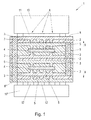
- connection system for electronic components is denoted by reference numeral 1.
- the connection system for electronic components consists of a plurality of insulating layers 2 and conductive layers 3 which make up the layered structure of the connection system for electronic components.
- the central insulating layer 2 and the two conductive layers 3 covering this central insulating layer 2 form the central core of the inventive connection system for electronic components 1.
- Embedded components 4 are embedded within insulating layers 2 of the connection system for electronic components 1, in this example the embedded components 4 take the form of gallium-nitride power transistors which are contacted by electric vias 5 to corresponding conductive layers 3 which are appropriately patterned to contact and drive the power transistors 4.
- a conductive adhesive 11 can be interposed between the surface of the connection system for electronic components 1 and the surface-mounted component 10, however, the heat delivered by the thermal duct 6 can also migrate into the second surface-mounted component 10' by solder balls 12 arranged on the second surface-mounted component 10' and being in contact with the surface 8 of the connection system for electronic components 1.
Landscapes
- Engineering & Computer Science (AREA)
- Microelectronics & Electronic Packaging (AREA)
- Physics & Mathematics (AREA)
- Thermal Sciences (AREA)
- Production Of Multi-Layered Print Wiring Board (AREA)
- Structure Of Printed Boards (AREA)
- Cooling Or The Like Of Semiconductors Or Solid State Devices (AREA)
- Manufacturing & Machinery (AREA)
Priority Applications (2)
| Application Number | Priority Date | Filing Date | Title |
|---|---|---|---|
| EP15186707.4A EP3148300B1 (fr) | 2015-09-24 | 2015-09-24 | Système de connexion pour composants électroniques |
| US15/272,568 US9698130B2 (en) | 2015-09-24 | 2016-09-22 | Connection system for electronic components |
Applications Claiming Priority (1)
| Application Number | Priority Date | Filing Date | Title |
|---|---|---|---|
| EP15186707.4A EP3148300B1 (fr) | 2015-09-24 | 2015-09-24 | Système de connexion pour composants électroniques |
Publications (2)
| Publication Number | Publication Date |
|---|---|
| EP3148300A1 true EP3148300A1 (fr) | 2017-03-29 |
| EP3148300B1 EP3148300B1 (fr) | 2023-07-26 |
Family
ID=54199593
Family Applications (1)
| Application Number | Title | Priority Date | Filing Date |
|---|---|---|---|
| EP15186707.4A Active EP3148300B1 (fr) | 2015-09-24 | 2015-09-24 | Système de connexion pour composants électroniques |
Country Status (2)
| Country | Link |
|---|---|
| US (1) | US9698130B2 (fr) |
| EP (1) | EP3148300B1 (fr) |
Cited By (2)
| Publication number | Priority date | Publication date | Assignee | Title |
|---|---|---|---|---|
| EP3481161A1 (fr) | 2017-11-02 | 2019-05-08 | AT & S Austria Technologie & Systemtechnik Aktiengesellschaft | Support de composant ayant des composants de transistor disposés côte à côte |
| EP3716326A1 (fr) * | 2019-03-25 | 2020-09-30 | Mitsubishi Electric R&D Centre Europe B.V. | Ensemble d'alimentation électrique comportant des couches électriquement conductrices épaisses |
Families Citing this family (7)
| Publication number | Priority date | Publication date | Assignee | Title |
|---|---|---|---|---|
| US10276585B2 (en) | 2016-08-12 | 2019-04-30 | Toshiba Memory Corporation | Semiconductor memory device |
| CN111164899B (zh) * | 2017-09-29 | 2022-05-10 | 株式会社村田制作所 | 高频电路以及通信装置 |
| US20200161206A1 (en) * | 2018-11-20 | 2020-05-21 | Advanced Semiconductor Engineering, Inc. | Semiconductor package structure and semiconductor manufacturing process |
| US10912195B2 (en) | 2019-01-02 | 2021-02-02 | The Boeing Company | Multi-embedded radio frequency board and mobile device including the same |
| US10462937B1 (en) | 2019-04-11 | 2019-10-29 | Borgwarner, Inc. | PCB design for electrically-actuated turbochargers |
| JP7318428B2 (ja) * | 2019-09-04 | 2023-08-01 | Tdk株式会社 | 電子部品内蔵回路基板及びその製造方法 |
| EP3869923B1 (fr) * | 2020-02-20 | 2025-01-08 | AT & S Austria Technologie & Systemtechnik Aktiengesellschaft | Intégration de profil de refroidissement pour systèmes d'alimentation intégrés |
Citations (4)
| Publication number | Priority date | Publication date | Assignee | Title |
|---|---|---|---|---|
| US20050207133A1 (en) * | 2004-03-11 | 2005-09-22 | Mark Pavier | Embedded power management control circuit |
| US20100025082A1 (en) * | 2006-12-18 | 2010-02-04 | Kenji Sasaoka | Electronic component built-in wiring board and method for radiating heat generated at the same |
| US20120227261A1 (en) * | 2011-03-11 | 2012-09-13 | Ibiden Co., Ltd. | Method for manufacturing printed wiring board |
| US20140110820A1 (en) * | 2012-10-18 | 2014-04-24 | Infineon Technologies Austria Ag | Passive component as thermal capacitance and heat sink |
Family Cites Families (9)
| Publication number | Priority date | Publication date | Assignee | Title |
|---|---|---|---|---|
| US20080318055A1 (en) | 2007-06-21 | 2008-12-25 | General Electric Company | Recoverable electronic component |
| US8914974B2 (en) | 2008-10-30 | 2014-12-23 | At & S Austria Technologie & Systemtechnik Aktiengesellschaft | Method for integrating an electronic component into a printed circuit board |
| KR101055509B1 (ko) | 2009-03-19 | 2011-08-08 | 삼성전기주식회사 | 전자부품 내장형 인쇄회로기판 |
| JP5624699B1 (ja) * | 2012-12-21 | 2014-11-12 | パナソニック株式会社 | 電子部品パッケージおよびその製造方法 |
| JP6116949B2 (ja) | 2013-03-14 | 2017-04-19 | 新光電気工業株式会社 | 発光素子搭載用の配線基板、発光装置、発光素子搭載用の配線基板の製造方法及び発光装置の製造方法 |
| AT514085B1 (de) * | 2013-06-11 | 2014-10-15 | Austria Tech & System Tech | Leistungsmodul |
| EP2911486B1 (fr) * | 2014-02-19 | 2024-07-31 | AT & S Austria Technologie & Systemtechnik Aktiengesellschaft | Dispositif de connecteur à PCB |
| SG10201400390YA (en) * | 2014-03-05 | 2015-10-29 | Delta Electronics Int L Singapore Pte Ltd | Package structure |
| EP3091822A1 (fr) * | 2015-05-08 | 2016-11-09 | AT & S Austria Technologie & Systemtechnik Aktiengesellschaft | Procédé pour la production d'un module électronique ainsi que module électronique correspondant |
-
2015
- 2015-09-24 EP EP15186707.4A patent/EP3148300B1/fr active Active
-
2016
- 2016-09-22 US US15/272,568 patent/US9698130B2/en active Active
Patent Citations (4)
| Publication number | Priority date | Publication date | Assignee | Title |
|---|---|---|---|---|
| US20050207133A1 (en) * | 2004-03-11 | 2005-09-22 | Mark Pavier | Embedded power management control circuit |
| US20100025082A1 (en) * | 2006-12-18 | 2010-02-04 | Kenji Sasaoka | Electronic component built-in wiring board and method for radiating heat generated at the same |
| US20120227261A1 (en) * | 2011-03-11 | 2012-09-13 | Ibiden Co., Ltd. | Method for manufacturing printed wiring board |
| US20140110820A1 (en) * | 2012-10-18 | 2014-04-24 | Infineon Technologies Austria Ag | Passive component as thermal capacitance and heat sink |
Cited By (7)
| Publication number | Priority date | Publication date | Assignee | Title |
|---|---|---|---|---|
| EP3481161A1 (fr) | 2017-11-02 | 2019-05-08 | AT & S Austria Technologie & Systemtechnik Aktiengesellschaft | Support de composant ayant des composants de transistor disposés côte à côte |
| US10973113B2 (en) | 2017-11-02 | 2021-04-06 | At&S Austria Technologie & Systemtechnik Aktiengesellschaft | Component carrier with transistor components arranged side by side |
| EP4604177A2 (fr) | 2017-11-02 | 2025-08-20 | AT & S Austria Technologie & Systemtechnik Aktiengesellschaft | Support de composant avec composants de transistor disposés côte à côte |
| EP3716326A1 (fr) * | 2019-03-25 | 2020-09-30 | Mitsubishi Electric R&D Centre Europe B.V. | Ensemble d'alimentation électrique comportant des couches électriquement conductrices épaisses |
| WO2020195089A1 (fr) * | 2019-03-25 | 2020-10-01 | Mitsubishi Electric Corporation | Ensemble d'alimentation électrique à couches électriquement conductrices épaisses |
| JP2022515931A (ja) * | 2019-03-25 | 2022-02-22 | ミツビシ・エレクトリック・アールアンドディー・センター・ヨーロッパ・ビーヴィ | 厚い導電層を備える電気パワーアセンブリ |
| US11791254B2 (en) | 2019-03-25 | 2023-10-17 | Mitsubishi Electric Corporation | Electrically power assembly with thick electrically conductive layers |
Also Published As
| Publication number | Publication date |
|---|---|
| US9698130B2 (en) | 2017-07-04 |
| EP3148300B1 (fr) | 2023-07-26 |
| US20170092630A1 (en) | 2017-03-30 |
Similar Documents
| Publication | Publication Date | Title |
|---|---|---|
| US9698130B2 (en) | Connection system for electronic components | |
| EP3481161B1 (fr) | Support de composant ayant des composants de transistor disposés côte à côte | |
| US10699986B2 (en) | Cooled electronics package with stacked power electronics components | |
| CN106953504B (zh) | 电子的线路单元 | |
| US20090078456A1 (en) | Three dimensional packaging optimized for high frequency circuitry | |
| US20190198423A1 (en) | Device module embedded with switch chip and manufacturing method thereof | |
| US9386686B2 (en) | Metal core printed circuit board and electronic package structure | |
| WO2014162478A1 (fr) | Substrat à composants intégrés et son procédé de fabrication | |
| US10498116B2 (en) | Three-dimensional power distribution interconnect structure | |
| TWI679734B (zh) | 電子模組及其製造方法 | |
| US11051432B2 (en) | Electronic module, in particular an electronic power module for hybrid vehicles or electric vehicles | |
| US9924590B2 (en) | Printed board and electronic apparatus | |
| US10212802B2 (en) | Electronic device and method for producing an electronic device | |
| US9609741B1 (en) | Printed circuit board and electronic apparatus | |
| US20170079130A1 (en) | Heat Spreader in Multilayer Build Ups | |
| KR20210018811A (ko) | 열 전도성 전자장치 패키징 | |
| US11653473B2 (en) | Integrated electrical bus bars in liquid coldplate with high density interconnects | |
| TWI738019B (zh) | 用於射頻組件之多堆疊冷卻結構 | |
| Thelemann et al. | Advancing packaging solutions using 3D capabilities of ceramic multilayers | |
| EP3086627B1 (fr) | Ascenseur comprenant une unité d'alimentation | |
| CN120770074A (zh) | 功率模块、逆变器以及机电装置 | |
| CN117476574A (zh) | 功率模块和包括其的逆变器及机电装置 |
Legal Events
| Date | Code | Title | Description |
|---|---|---|---|
| PUAI | Public reference made under article 153(3) epc to a published international application that has entered the european phase |
Free format text: ORIGINAL CODE: 0009012 |
|
| STAA | Information on the status of an ep patent application or granted ep patent |
Free format text: STATUS: THE APPLICATION HAS BEEN PUBLISHED |
|
| AK | Designated contracting states |
Kind code of ref document: A1 Designated state(s): AL AT BE BG CH CY CZ DE DK EE ES FI FR GB GR HR HU IE IS IT LI LT LU LV MC MK MT NL NO PL PT RO RS SE SI SK SM TR |
|
| AX | Request for extension of the european patent |
Extension state: BA ME |
|
| STAA | Information on the status of an ep patent application or granted ep patent |
Free format text: STATUS: REQUEST FOR EXAMINATION WAS MADE |
|
| 17P | Request for examination filed |
Effective date: 20170921 |
|
| RBV | Designated contracting states (corrected) |
Designated state(s): AL AT BE BG CH CY CZ DE DK EE ES FI FR GB GR HR HU IE IS IT LI LT LU LV MC MK MT NL NO PL PT RO RS SE SI SK SM TR |
|
| STAA | Information on the status of an ep patent application or granted ep patent |
Free format text: STATUS: EXAMINATION IS IN PROGRESS |
|
| 17Q | First examination report despatched |
Effective date: 20200113 |
|
| GRAP | Despatch of communication of intention to grant a patent |
Free format text: ORIGINAL CODE: EPIDOSNIGR1 |
|
| STAA | Information on the status of an ep patent application or granted ep patent |
Free format text: STATUS: GRANT OF PATENT IS INTENDED |
|
| RIC1 | Information provided on ipc code assigned before grant |
Ipc: H01L 25/10 19740701ALI20230109BHEP Ipc: H01L 23/00 19740701ALI20230109BHEP Ipc: H01L 23/538 19900101ALI20230109BHEP Ipc: H01L 23/367 19900101ALI20230109BHEP Ipc: H05K 1/02 19680901ALI20230109BHEP Ipc: H05K 1/18 19680901AFI20230109BHEP |
|
| INTG | Intention to grant announced |
Effective date: 20230210 |
|
| RAP3 | Party data changed (applicant data changed or rights of an application transferred) |
Owner name: AT & S AUSTRIA TECHNOLOGIE & SYSTEMTECHNIK AKTIENGESELLSCHAFT |
|
| GRAS | Grant fee paid |
Free format text: ORIGINAL CODE: EPIDOSNIGR3 |
|
| GRAA | (expected) grant |
Free format text: ORIGINAL CODE: 0009210 |
|
| STAA | Information on the status of an ep patent application or granted ep patent |
Free format text: STATUS: THE PATENT HAS BEEN GRANTED |
|
| AK | Designated contracting states |
Kind code of ref document: B1 Designated state(s): AL AT BE BG CH CY CZ DE DK EE ES FI FR GB GR HR HU IE IS IT LI LT LU LV MC MK MT NL NO PL PT RO RS SE SI SK SM TR |
|
| REG | Reference to a national code |
Ref country code: CH Ref legal event code: EP |
|
| REG | Reference to a national code |
Ref country code: IE Ref legal event code: FG4D |
|
| REG | Reference to a national code |
Ref country code: DE Ref legal event code: R096 Ref document number: 602015084738 Country of ref document: DE |
|
| P01 | Opt-out of the competence of the unified patent court (upc) registered |
Effective date: 20230824 |
|
| REG | Reference to a national code |
Ref country code: LT Ref legal event code: MG9D |
|
| REG | Reference to a national code |
Ref country code: NL Ref legal event code: MP Effective date: 20230726 |
|
| REG | Reference to a national code |
Ref country code: AT Ref legal event code: MK05 Ref document number: 1593481 Country of ref document: AT Kind code of ref document: T Effective date: 20230726 |
|
| PG25 | Lapsed in a contracting state [announced via postgrant information from national office to epo] |
Ref country code: NL Free format text: LAPSE BECAUSE OF FAILURE TO SUBMIT A TRANSLATION OF THE DESCRIPTION OR TO PAY THE FEE WITHIN THE PRESCRIBED TIME-LIMIT Effective date: 20230726 |
|
| PG25 | Lapsed in a contracting state [announced via postgrant information from national office to epo] |
Ref country code: GR Free format text: LAPSE BECAUSE OF FAILURE TO SUBMIT A TRANSLATION OF THE DESCRIPTION OR TO PAY THE FEE WITHIN THE PRESCRIBED TIME-LIMIT Effective date: 20231027 |
|
| PG25 | Lapsed in a contracting state [announced via postgrant information from national office to epo] |
Ref country code: IS Free format text: LAPSE BECAUSE OF FAILURE TO SUBMIT A TRANSLATION OF THE DESCRIPTION OR TO PAY THE FEE WITHIN THE PRESCRIBED TIME-LIMIT Effective date: 20231126 |
|
| PG25 | Lapsed in a contracting state [announced via postgrant information from national office to epo] |
Ref country code: SE Free format text: LAPSE BECAUSE OF FAILURE TO SUBMIT A TRANSLATION OF THE DESCRIPTION OR TO PAY THE FEE WITHIN THE PRESCRIBED TIME-LIMIT Effective date: 20230726 Ref country code: RS Free format text: LAPSE BECAUSE OF FAILURE TO SUBMIT A TRANSLATION OF THE DESCRIPTION OR TO PAY THE FEE WITHIN THE PRESCRIBED TIME-LIMIT Effective date: 20230726 Ref country code: PT Free format text: LAPSE BECAUSE OF FAILURE TO SUBMIT A TRANSLATION OF THE DESCRIPTION OR TO PAY THE FEE WITHIN THE PRESCRIBED TIME-LIMIT Effective date: 20231127 Ref country code: NO Free format text: LAPSE BECAUSE OF FAILURE TO SUBMIT A TRANSLATION OF THE DESCRIPTION OR TO PAY THE FEE WITHIN THE PRESCRIBED TIME-LIMIT Effective date: 20231026 Ref country code: LV Free format text: LAPSE BECAUSE OF FAILURE TO SUBMIT A TRANSLATION OF THE DESCRIPTION OR TO PAY THE FEE WITHIN THE PRESCRIBED TIME-LIMIT Effective date: 20230726 Ref country code: LT Free format text: LAPSE BECAUSE OF FAILURE TO SUBMIT A TRANSLATION OF THE DESCRIPTION OR TO PAY THE FEE WITHIN THE PRESCRIBED TIME-LIMIT Effective date: 20230726 Ref country code: IS Free format text: LAPSE BECAUSE OF FAILURE TO SUBMIT A TRANSLATION OF THE DESCRIPTION OR TO PAY THE FEE WITHIN THE PRESCRIBED TIME-LIMIT Effective date: 20231126 Ref country code: HR Free format text: LAPSE BECAUSE OF FAILURE TO SUBMIT A TRANSLATION OF THE DESCRIPTION OR TO PAY THE FEE WITHIN THE PRESCRIBED TIME-LIMIT Effective date: 20230726 Ref country code: GR Free format text: LAPSE BECAUSE OF FAILURE TO SUBMIT A TRANSLATION OF THE DESCRIPTION OR TO PAY THE FEE WITHIN THE PRESCRIBED TIME-LIMIT Effective date: 20231027 Ref country code: FI Free format text: LAPSE BECAUSE OF FAILURE TO SUBMIT A TRANSLATION OF THE DESCRIPTION OR TO PAY THE FEE WITHIN THE PRESCRIBED TIME-LIMIT Effective date: 20230726 Ref country code: AT Free format text: LAPSE BECAUSE OF FAILURE TO SUBMIT A TRANSLATION OF THE DESCRIPTION OR TO PAY THE FEE WITHIN THE PRESCRIBED TIME-LIMIT Effective date: 20230726 |
|
| PG25 | Lapsed in a contracting state [announced via postgrant information from national office to epo] |
Ref country code: PL Free format text: LAPSE BECAUSE OF FAILURE TO SUBMIT A TRANSLATION OF THE DESCRIPTION OR TO PAY THE FEE WITHIN THE PRESCRIBED TIME-LIMIT Effective date: 20230726 |
|
| PG25 | Lapsed in a contracting state [announced via postgrant information from national office to epo] |
Ref country code: ES Free format text: LAPSE BECAUSE OF FAILURE TO SUBMIT A TRANSLATION OF THE DESCRIPTION OR TO PAY THE FEE WITHIN THE PRESCRIBED TIME-LIMIT Effective date: 20230726 |
|
| REG | Reference to a national code |
Ref country code: DE Ref legal event code: R097 Ref document number: 602015084738 Country of ref document: DE |
|
| PG25 | Lapsed in a contracting state [announced via postgrant information from national office to epo] |
Ref country code: SM Free format text: LAPSE BECAUSE OF FAILURE TO SUBMIT A TRANSLATION OF THE DESCRIPTION OR TO PAY THE FEE WITHIN THE PRESCRIBED TIME-LIMIT Effective date: 20230726 Ref country code: RO Free format text: LAPSE BECAUSE OF FAILURE TO SUBMIT A TRANSLATION OF THE DESCRIPTION OR TO PAY THE FEE WITHIN THE PRESCRIBED TIME-LIMIT Effective date: 20230726 Ref country code: ES Free format text: LAPSE BECAUSE OF FAILURE TO SUBMIT A TRANSLATION OF THE DESCRIPTION OR TO PAY THE FEE WITHIN THE PRESCRIBED TIME-LIMIT Effective date: 20230726 Ref country code: EE Free format text: LAPSE BECAUSE OF FAILURE TO SUBMIT A TRANSLATION OF THE DESCRIPTION OR TO PAY THE FEE WITHIN THE PRESCRIBED TIME-LIMIT Effective date: 20230726 Ref country code: DK Free format text: LAPSE BECAUSE OF FAILURE TO SUBMIT A TRANSLATION OF THE DESCRIPTION OR TO PAY THE FEE WITHIN THE PRESCRIBED TIME-LIMIT Effective date: 20230726 Ref country code: CZ Free format text: LAPSE BECAUSE OF FAILURE TO SUBMIT A TRANSLATION OF THE DESCRIPTION OR TO PAY THE FEE WITHIN THE PRESCRIBED TIME-LIMIT Effective date: 20230726 Ref country code: SK Free format text: LAPSE BECAUSE OF FAILURE TO SUBMIT A TRANSLATION OF THE DESCRIPTION OR TO PAY THE FEE WITHIN THE PRESCRIBED TIME-LIMIT Effective date: 20230726 |
|
| REG | Reference to a national code |
Ref country code: CH Ref legal event code: PL |
|
| PG25 | Lapsed in a contracting state [announced via postgrant information from national office to epo] |
Ref country code: LU Free format text: LAPSE BECAUSE OF NON-PAYMENT OF DUE FEES Effective date: 20230924 |
|
| REG | Reference to a national code |
Ref country code: BE Ref legal event code: MM Effective date: 20230930 |
|
| PG25 | Lapsed in a contracting state [announced via postgrant information from national office to epo] |
Ref country code: LU Free format text: LAPSE BECAUSE OF NON-PAYMENT OF DUE FEES Effective date: 20230924 Ref country code: IT Free format text: LAPSE BECAUSE OF FAILURE TO SUBMIT A TRANSLATION OF THE DESCRIPTION OR TO PAY THE FEE WITHIN THE PRESCRIBED TIME-LIMIT Effective date: 20230726 Ref country code: MC Free format text: LAPSE BECAUSE OF FAILURE TO SUBMIT A TRANSLATION OF THE DESCRIPTION OR TO PAY THE FEE WITHIN THE PRESCRIBED TIME-LIMIT Effective date: 20230726 |
|
| PLBE | No opposition filed within time limit |
Free format text: ORIGINAL CODE: 0009261 |
|
| STAA | Information on the status of an ep patent application or granted ep patent |
Free format text: STATUS: NO OPPOSITION FILED WITHIN TIME LIMIT |
|
| GBPC | Gb: european patent ceased through non-payment of renewal fee |
Effective date: 20231026 |
|
| 26N | No opposition filed |
Effective date: 20240429 |
|
| REG | Reference to a national code |
Ref country code: IE Ref legal event code: MM4A |
|
| PG25 | Lapsed in a contracting state [announced via postgrant information from national office to epo] |
Ref country code: IE Free format text: LAPSE BECAUSE OF NON-PAYMENT OF DUE FEES Effective date: 20230924 |
|
| PG25 | Lapsed in a contracting state [announced via postgrant information from national office to epo] |
Ref country code: GB Free format text: LAPSE BECAUSE OF NON-PAYMENT OF DUE FEES Effective date: 20231026 |
|
| PG25 | Lapsed in a contracting state [announced via postgrant information from national office to epo] |
Ref country code: CH Free format text: LAPSE BECAUSE OF NON-PAYMENT OF DUE FEES Effective date: 20230930 |
|
| PG25 | Lapsed in a contracting state [announced via postgrant information from national office to epo] |
Ref country code: IE Free format text: LAPSE BECAUSE OF NON-PAYMENT OF DUE FEES Effective date: 20230924 Ref country code: GB Free format text: LAPSE BECAUSE OF NON-PAYMENT OF DUE FEES Effective date: 20231026 Ref country code: CH Free format text: LAPSE BECAUSE OF NON-PAYMENT OF DUE FEES Effective date: 20230930 Ref country code: SI Free format text: LAPSE BECAUSE OF FAILURE TO SUBMIT A TRANSLATION OF THE DESCRIPTION OR TO PAY THE FEE WITHIN THE PRESCRIBED TIME-LIMIT Effective date: 20230726 |
|
| PG25 | Lapsed in a contracting state [announced via postgrant information from national office to epo] |
Ref country code: BE Free format text: LAPSE BECAUSE OF NON-PAYMENT OF DUE FEES Effective date: 20230930 |
|
| PG25 | Lapsed in a contracting state [announced via postgrant information from national office to epo] |
Ref country code: BG Free format text: LAPSE BECAUSE OF FAILURE TO SUBMIT A TRANSLATION OF THE DESCRIPTION OR TO PAY THE FEE WITHIN THE PRESCRIBED TIME-LIMIT Effective date: 20230726 |
|
| PG25 | Lapsed in a contracting state [announced via postgrant information from national office to epo] |
Ref country code: BG Free format text: LAPSE BECAUSE OF FAILURE TO SUBMIT A TRANSLATION OF THE DESCRIPTION OR TO PAY THE FEE WITHIN THE PRESCRIBED TIME-LIMIT Effective date: 20230726 |
|
| PG25 | Lapsed in a contracting state [announced via postgrant information from national office to epo] |
Ref country code: CY Free format text: LAPSE BECAUSE OF FAILURE TO SUBMIT A TRANSLATION OF THE DESCRIPTION OR TO PAY THE FEE WITHIN THE PRESCRIBED TIME-LIMIT; INVALID AB INITIO Effective date: 20150924 |
|
| PG25 | Lapsed in a contracting state [announced via postgrant information from national office to epo] |
Ref country code: HU Free format text: LAPSE BECAUSE OF FAILURE TO SUBMIT A TRANSLATION OF THE DESCRIPTION OR TO PAY THE FEE WITHIN THE PRESCRIBED TIME-LIMIT; INVALID AB INITIO Effective date: 20150924 |
|
| PGFP | Annual fee paid to national office [announced via postgrant information from national office to epo] |
Ref country code: DE Payment date: 20250917 Year of fee payment: 11 |
|
| PGFP | Annual fee paid to national office [announced via postgrant information from national office to epo] |
Ref country code: FR Payment date: 20250926 Year of fee payment: 11 |
|
| PG25 | Lapsed in a contracting state [announced via postgrant information from national office to epo] |
Ref country code: TR Free format text: LAPSE BECAUSE OF FAILURE TO SUBMIT A TRANSLATION OF THE DESCRIPTION OR TO PAY THE FEE WITHIN THE PRESCRIBED TIME-LIMIT Effective date: 20230726 |