EP3149092B1 - Encre conductrice pour stylo à bille roulante et tracé conducteur formé sur un substrat - Google Patents
Encre conductrice pour stylo à bille roulante et tracé conducteur formé sur un substrat Download PDFInfo
- Publication number
- EP3149092B1 EP3149092B1 EP15799641.4A EP15799641A EP3149092B1 EP 3149092 B1 EP3149092 B1 EP 3149092B1 EP 15799641 A EP15799641 A EP 15799641A EP 3149092 B1 EP3149092 B1 EP 3149092B1
- Authority
- EP
- European Patent Office
- Prior art keywords
- conductive
- ink
- trace
- flakes
- particles
- Prior art date
- Legal status (The legal status is an assumption and is not a legal conclusion. Google has not performed a legal analysis and makes no representation as to the accuracy of the status listed.)
- Active
Links
Images

Classifications
-
- C—CHEMISTRY; METALLURGY
- C09—DYES; PAINTS; POLISHES; NATURAL RESINS; ADHESIVES; COMPOSITIONS NOT OTHERWISE PROVIDED FOR; APPLICATIONS OF MATERIALS NOT OTHERWISE PROVIDED FOR
- C09D—COATING COMPOSITIONS, e.g. PAINTS, VARNISHES OR LACQUERS; FILLING PASTES; CHEMICAL PAINT OR INK REMOVERS; INKS; CORRECTING FLUIDS; WOODSTAINS; PASTES OR SOLIDS FOR COLOURING OR PRINTING; USE OF MATERIALS THEREFOR
- C09D11/00—Inks
- C09D11/52—Electrically conductive inks
-
- C—CHEMISTRY; METALLURGY
- C09—DYES; PAINTS; POLISHES; NATURAL RESINS; ADHESIVES; COMPOSITIONS NOT OTHERWISE PROVIDED FOR; APPLICATIONS OF MATERIALS NOT OTHERWISE PROVIDED FOR
- C09D—COATING COMPOSITIONS, e.g. PAINTS, VARNISHES OR LACQUERS; FILLING PASTES; CHEMICAL PAINT OR INK REMOVERS; INKS; CORRECTING FLUIDS; WOODSTAINS; PASTES OR SOLIDS FOR COLOURING OR PRINTING; USE OF MATERIALS THEREFOR
- C09D11/00—Inks
- C09D11/16—Writing inks
- C09D11/18—Writing inks specially adapted for ball-point writing instruments
-
- H—ELECTRICITY
- H01—ELECTRIC ELEMENTS
- H01B—CABLES; CONDUCTORS; INSULATORS; SELECTION OF MATERIALS FOR THEIR CONDUCTIVE, INSULATING OR DIELECTRIC PROPERTIES
- H01B1/00—Conductors or conductive bodies characterised by the conductive materials; Selection of materials as conductors
- H01B1/02—Conductors or conductive bodies characterised by the conductive materials; Selection of materials as conductors mainly consisting of metals or alloys
-
- H—ELECTRICITY
- H05—ELECTRIC TECHNIQUES NOT OTHERWISE PROVIDED FOR
- H05K—PRINTED CIRCUITS; CASINGS OR CONSTRUCTIONAL DETAILS OF ELECTRIC APPARATUS; MANUFACTURE OF ASSEMBLAGES OF ELECTRICAL COMPONENTS
- H05K1/00—Printed circuits
- H05K1/02—Details
- H05K1/0274—Optical details, e.g. printed circuits comprising integral optical means
-
- H—ELECTRICITY
- H05—ELECTRIC TECHNIQUES NOT OTHERWISE PROVIDED FOR
- H05K—PRINTED CIRCUITS; CASINGS OR CONSTRUCTIONAL DETAILS OF ELECTRIC APPARATUS; MANUFACTURE OF ASSEMBLAGES OF ELECTRICAL COMPONENTS
- H05K1/00—Printed circuits
- H05K1/02—Details
- H05K1/09—Use of materials for the conductive, e.g. metallic pattern
- H05K1/092—Dispersed materials, e.g. conductive pastes or inks
- H05K1/097—Inks comprising nanoparticles and specially adapted for being sintered at low temperature
-
- C—CHEMISTRY; METALLURGY
- C01—INORGANIC CHEMISTRY
- C01P—INDEXING SCHEME RELATING TO STRUCTURAL AND PHYSICAL ASPECTS OF SOLID INORGANIC COMPOUNDS
- C01P2004/00—Particle morphology
- C01P2004/30—Particle morphology extending in three dimensions
- C01P2004/32—Spheres
-
- C—CHEMISTRY; METALLURGY
- C01—INORGANIC CHEMISTRY
- C01P—INDEXING SCHEME RELATING TO STRUCTURAL AND PHYSICAL ASPECTS OF SOLID INORGANIC COMPOUNDS
- C01P2004/00—Particle morphology
- C01P2004/60—Particles characterised by their size
- C01P2004/64—Nanometer sized, i.e. from 1-100 nanometer
-
- C—CHEMISTRY; METALLURGY
- C01—INORGANIC CHEMISTRY
- C01P—INDEXING SCHEME RELATING TO STRUCTURAL AND PHYSICAL ASPECTS OF SOLID INORGANIC COMPOUNDS
- C01P2006/00—Physical properties of inorganic compounds
- C01P2006/40—Electric properties
-
- H—ELECTRICITY
- H05—ELECTRIC TECHNIQUES NOT OTHERWISE PROVIDED FOR
- H05K—PRINTED CIRCUITS; CASINGS OR CONSTRUCTIONAL DETAILS OF ELECTRIC APPARATUS; MANUFACTURE OF ASSEMBLAGES OF ELECTRICAL COMPONENTS
- H05K2201/00—Indexing scheme relating to printed circuits covered by H05K1/00
- H05K2201/02—Fillers; Particles; Fibers; Reinforcement materials
- H05K2201/0203—Fillers and particles
- H05K2201/0242—Shape of an individual particle
- H05K2201/0245—Flakes, flat particles or lamellar particles
-
- H—ELECTRICITY
- H05—ELECTRIC TECHNIQUES NOT OTHERWISE PROVIDED FOR
- H05K—PRINTED CIRCUITS; CASINGS OR CONSTRUCTIONAL DETAILS OF ELECTRIC APPARATUS; MANUFACTURE OF ASSEMBLAGES OF ELECTRICAL COMPONENTS
- H05K2201/00—Indexing scheme relating to printed circuits covered by H05K1/00
- H05K2201/02—Fillers; Particles; Fibers; Reinforcement materials
- H05K2201/0203—Fillers and particles
- H05K2201/0242—Shape of an individual particle
- H05K2201/0257—Nanoparticles
Definitions
- the present disclosure is related generally to ink formulations more particularly to a conductive ink that may be written onto paper and other substrates to form conductive traces.
- Printed electronics constitute an emerging class of materials with potential application in photovoltaics, transistors, displays, batteries, antennas, and sensors. Recent attention has focused on paper substrates as a low-cost, enabling platform for flexible, lightweight, and disposable devices. Such devices require conductive electrodes, which, to date, have been deposited by sputter coating, inkjet printing, and airbrush spraying. However, these deposition methods may be costly or may employ dilute inks that readily permeate the paper substrate.
- Paper substrates offer many advantages for printed electronic devices. Not only is paper widely available and inexpensive, it is lightweight, biodegradable, and can be rolled or folded into three-dimensional (3D) configurations. Functional electronic components, including thermochromic displays, disposable radio frequency identification (RFID) tags, and cellulose-based batteries have recently been produced on paper substrates. The wide variety of available paper textures, compositions, and coatings can be exploited to enable specific device architectures. Facile routes to creating devices "on-the-fly" under ambient conditions could make it possible to fully exploit the potential of paper-based printed electronics.
- RFID radio frequency identification
- a conductive ink for a rollerball pen comprises an aqueous solvent and conductive particles comprising one or more metals dispersed therein at a concentration of at least 30 wt.%.
- the conductive particles include conductive flakes and conductive nanoparticles.
- a dispersant coats the conductive particles at a loading level of at least 0.1 mg/m 2 to 0.8 mg/m 2 .
- a conductive trace deposited on a substrate from a rollerball pen comprises a percolative network of conductive particles comprising one or more metals.
- the conductive particles include conductive flakes and conductive nanoparticles.
- the conductive trace has a conductivity of at least about 1% of a bulk metal conductivity and a reflectance of greater than 40%.
- a conductive trace formed by: providing a conductive ink in a rollerball pen; moving the rollerban pen over a surface to deposit the conductive ink on the surface; and drying the conductive ink at room temperature, thereby forming the conductive trace.
- the conductive ink comprises an aqueous solvent and conductive particles comprising one or more metals dispersed therein at a concentration of at least 30 wt.%.
- the conductive particles include conductive flakes and conductive nanoparticles.
- a dispersant coats the conductive particles at a loading level of from 0.1 mg/m 2 to 0.8 mg/m 2 .
- a method of forming a conductive trace comprises providing a conductive ink in a rollerball pen, moving the rollerball pen over a surface to deposit the conductive ink on the surface, and drying the conductive ink at room temperature, thereby forming the conductive trace.
- the conductive ink comprises an aqueous solvent and conductive particles comprising one or more metals dispersed therein at a concentration of at least 30 wt.%.
- the conductive particles comprise conductive flakes and conductive nanoparticles, and a dispersant coats the conductive particles at a loading level of from 0.1 mg/m 2 to 0.8 mg/m 2 .
- a highly stable and quick-drying conductive ink formulation has been developed for use with a rollerball pen to form conductive traces on a wide range of substrates.
- the conductive traces comprise a metal such as silver and may exhibit a conductivity up to 20% of a bulk conductivity of the metal.
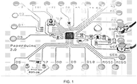
- the conductive ink may be deposited onto paper, plastic, and other flexible or rigid substrates to form traces that serve as the wiring for electronic devices, as shown for example in FIG. 1 .
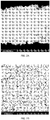
- FIGs. 2A and 2B show scanning electron microscopy (SEM) images at two different magnifications of an exemplary conductive trace formed on copy paper
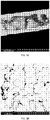
- FIGs. 3A and 3B show SEM images at two different magnifications of an exemplary conductive trace formed on photo paper.
- the conductive trace comprises a percolative network of conductive particles comprising silver.
- the conductive particles may include conductive particles of different sizes and morphologies, including flakes and nanoparticles.
- the conductive ink used to form the traces comprises an aqueous solvent and conductive particles comprising one or more metals dispersed therein at a concentration of at least 30 wt.%.
- a dispersant coats the conductive particles at a loading level of from 0.1 mg/m 2 to 0.8 mg/m 2 .
- the conductive particles include the conductive flakes and conductive nanoparticles shown for example in FIG. 2B after deposition.
- a low resistance conductive trace may be formed when the ink is deposited onto paper (or another substrate). Also, the use of conductive particles having a bimodal size distribution and/or different morphologies may improve particle packing in the conductive trace, and thus promote percolation (formation of an electrically continuous path through the conductive particles).
- the conductive ink has a long shelf life or dispersion stability, which, as would be recognized by one of ordinary skill in the art, may be in conflict with achieving a high solids (particle) loading.
- a dispersant to enhance the stability of the ink may also detrimentally affect the conductivity of the trace written on the substrate.
- the inventors have found that, by using an amount of dispersant in the range of 0.1 mg/m 2 to 0.8 mg/m 2 , combined with a suitable ratio of conductive flakes to conductive nanoparticles as discussed below, a stable and quick-drying conductive ink can be formed even at high solids loading levels.
- the conductive ink When applied to a substrate such as paper using a rollerball pen, the conductive ink dries to form a highly conductive trace that also features high reflectivity and good adhesion to the substrate.
- the concentration of the conductive particles in the ink is at least 40 wt.%, at least 50 wt.%, at least 60 wt.%, at least 70 wt.%, or at least 80 wt.%.
- the concentration may also be as high as 85 wt.%, or as high as 90 wt.%.
- the amount of the dispersant may be at least 0.2 mg/m 2 , at least 0.3 mg/m 2 , at least 0.4 mg/m 2 , or at least 0.5 mg/m 2 , where the units represent mass of the dispersant in mg per m 2 of surface area of the conductive particles. Typically, the amount of the dispersant does not exceed 0.7 mg/m 2 or 0.8 mg/m 2 . When adsorbed to the surfaces of the conductive particles (flakes and/or nanoparticles), the dispersant prevents or minimizes aggregation, thereby enhancing the stability of the ink composition. If an amount in excess of 0.8 mg/m 2 is used, however, it may inhibit electrical contact between the conductive flakes and particles and reduce the conductivity of the conductive trace.
- the dispersant may comprise a polymer, such as a polyelectrolyte with a molecular weight greater than 1000 g/mol ( e . g ., polyvinylpyrrollidone (PVP), polyacrylic acid (PAA) and/or hydroxypropyl cellulose (HPC)).
- a polymer such as a polyelectrolyte with a molecular weight greater than 1000 g/mol (e . g ., polyvinylpyrrollidone (PVP), polyacrylic acid (PAA) and/or hydroxypropyl cellulose (HPC)).
- PVP polyvinylpyrrollidone
- PAA polyacrylic acid
- HPC hydroxypropyl cellulose
- the polymer may be selected from the group consisting of polyvinylpyrrollidone (PVP), polyacrylic acid (PAA), hydroxypropyl cellulose (HPC), polyvinylmethylether (PVME), polyvinyl alcohol (PVA), polyoxyethylene glycol sorbitan alkyl esters, polyoxypropylene glycol alkyl ethers, polyoxyethylene glycol alkyl ethers, and polyoxyethylene glycol octylphenol ethers.
- the dispersant may alternatively not comprise a polymer.
- the dispersant may be perfluorooctanesulfonate (PFOS) or perfluorononanoic acid (PFNA).
- the conductive flakes may have a plate-like morphology with an average thickness that is much smaller than an average lateral dimension of the flakes, where "lateral dimension” refers to a linear dimension (e . g ., width, length and/or diameter) measured normal to the thickness of the flake.
- lateral dimension refers to a linear dimension (e . g ., width, length and/or diameter) measured normal to the thickness of the flake.
- the average thickness of the conductive flakes is 1-2 orders of magnitude smaller than the average width (or other lateral dimension).
- the conductive flakes may have an average width of a few microns ( e . g ., 1-5 microns), while the average thickness of the conductive flakes may be tens to hundreds of nanometers.
- the average lateral dimension of the conductive flakes may be at least 500 nm, at least 750 nm, at least 1 micron, or at least 2 microns in size, and is typically no greater than 5 microns, no greater than 4 microns, or no greater than 3 microns.
- the average thickness of the conductive flakes may be at least 10 nm, at least 50 nm, or at least 100 nm, and is typically no greater than 300 nm, no greater than 200 nm, or no greater than 100 nm.
- the conductive nanoparticles may have a substantially spherical shape and thus may be referred to as conductive nanospheres. Alternatively, the conductive nanoparticles may have an irregular or other morphology, such as a faceted shape or an acicular shape.
- the conductive nanoparticles typically have an average linear dimension (length, width and/or diameter) of 500 nm or less, 200 nm or less, or 100 nm or less.
- the average linear dimension may also be at least 10 nm, at least 50 nm, or at least 100 nm.
- the average linear dimension of the conductive nanoparticles may range from 10 nm to 200 nm, or from 100 nm to 500 nm.
- the weight ratio may be at least 0.1:1, at least 1:1, at least 3:1, at least 6:1, or at least 9:1.
- the weight ratio is no greater than 20:1, or no greater than 15:1.
- the conductive particles including the conductive flakes and conductive nanoparticles may comprise one or more metals selected from the transition metals, the metalloids, and/or the rare earth metals.
- the one or more metals may be selected from the group consisting of: Al, Sc, Ti, V, Cr, Mn, Fe, Co, Ni, Cu, Y, Zr, Nb, Mo, Tc, Ru, Rh, Pd, Ag, In, Sn, Sb, Hf, Ta, W, Re, Os, Ir, Pt, and Au.
- Preferred metals may include Ag, Au, Cu, Ni, Pt, and/or Pd.
- the conductive particles may comprise substantially pure metals containing only incidental impurities, metal alloys, and/or metal oxides (e . g ., tin oxide or indium-tin oxide). It is also contemplated that the conductive particles may include a coating (e . g ., a conductive coating or a passivation layer) on individual flakes and/or particles. The coating may include one or more of the metals mentioned above.
- the conductive ink may further comprise a viscosifier to adjust the flow behavior of the ink.
- the viscosifier may be selected from among hydroxylethyl cellulose (HEC), xantham gum, and guar gum.
- HEC hydroxylethyl cellulose
- xantham gum xantham gum
- guar gum hydroxylethyl cellulose
- the viscosifier is HEC at a concentration of from 2 wt.% to 3 wt.% with respect to the conductive particles.
- the viscosity of the conductive ink may range from 4000 centipoise to 6000 centipoise under zero shear stress conditions.
- a surfactant may be added to the conductive ink to reduce surface tension and promote good wetting of the paper or other substrate.
- the surfactant may comprise a polymeric fluorosurfactant such as BYK® 340 (BYK-Chemie GmbH, Wesel, Germany).
- the conductive ink may be prepared by forming a mixture including the conductive flakes and nanoparticles in an aqueous solvent (such as water) along with the dispersant (e . g ., PAA).
- the mixture may be sonicated to ensure that the flakes and nanoparticles are well dispersed.
- a viscosifier may be added to increase the viscosity of the mixture, and a small amount of a surface tension modifier (surfactant) may also or alternatively be added to improve the smoothness of the dispensed ink on the paper or other substrate.
- the ink may be loaded into a rollerball pen for writing.
- Rollerball pens known in the art typically have ball diameters ranging from 250 microns to nearly one millimeter.
- a preferred range of rollerball pen diameters for use with the conductive ink is from 800 microns to 1000 microns.
- the conductive ink designed as described above may exhibit a dispersion stability or shelf life of at least 8 months, or at least 12 months.
- the shelf life may also be 24 months or more.
- the dispersion stability/shelf life is from 8 months to 12 months.
- a conductive trace may be formed from the conductive ink by first providing a conductive ink in a rollerball pen, where, as set forth above, the conductive ink comprises an aqueous solvent and conductive particles comprising one or more metals dispersed therein at a concentration of at least 30 wt.%, where the conductive particles include conductive flakes and conductive nanoparticles, and a dispersant coats the conductive particles at a loading level of from 0.1 mg/m 2 to 0.8 mg/m 2 .
- the rollerball pen is then moved over a surface to deposit the conductive ink on the surface.
- the conductive ink is dried at room temperature to form the conductive trace.
- the conductive ink is engineered to dry rapidly.
- a profilometer may be used to measure the cross-sectional area A.
- the conductive trace formed upon drying may comprise a percolative network of conductive particles comprising one or more metals, as shown for example in FIG. 2B .
- the conductive particles include conductive flakes and conductive nanoparticles, and the conductive trace may have a conductivity of at least 1% of a bulk metal conductivity, as explained below, and a reflectance of greater than 40%.
- the one or more metals of the conductive trace may be selected from the transition metals, the metalloids, and/or the rare earth metals.
- the one or more metals may be selected from the group consisting of: Al, Sc, Ti, V, Cr, Mn, Fe, Co, Ni, Cu, Y, Zr, Nb, Mo, Tc, Ru, Rh, Pd, Ag, In, Sn, Sb, Hf, Ta, W, Re, Os, Ir, Pt, and Au.
- Preferred metals may include Ag, Au, Cu, Ni, Pt, and/or Pd.
- the conductive particles may comprise substantially pure metals containing only incidental impurities, metal alloys, and/or metal oxides (e . g ., tin oxide or indium-tin oxide). It is also contemplated that the conductive particles may include a coating (e . g ., a conductive coating or a passivation layer) on individual flakes and/or particles. The coating may include one or more of the metals mentioned above.
- the conductive flakes and the conductive nanoparticles of the conductive trace may have any of the morphologies and sizes set forth above in the description of the conductive ink. Because the ink is deposited and dried at room temperature, excessive sintering may be avoided and the flakes and nanoparticles of the conductive trace may be similar or identical in morphology/size to those of the as-deposited conductive ink.
- an appropriate weight ratio of the conductive flakes to the conductive nanoparticles may be selected to achieve good particle packing and formation of a percolative network of conductive particles in the deposited conductive trace.
- the weight ratio may be at least 0.1:1, at least 1:1, at least 3:1, at least 6:1, or at least 9:1.
- the weight ratio is no greater than 20:1, or no greater than 15:1.
- the percolative network of conductive particles may comprise a dispersant coated thereon, and the dispersant may be present in an amount ranging from 0.1 mg/m 2 to 0.8 mg/m 2 , or from 0.5 mg/m 2 to 0.8 mg/m 2 .
- the conductive trace exhibits a conductivity of at least 0.1% of a bulk metal conductivity, where bulk metal conductivity refers to the bulk conductivity of the metal making up a primary portion of, or an entirety of, the conductive trace.
- the conductivity may also be at least about 1% of the bulk metal conductivity, at least 5% of the bulk metal conductivity, at least 10% of the bulk metal conductivity, or at least 15% of the bulk metal conductivity.
- the conductivity of the conductive trace (or the bulk metal) may be determined by measuring resistivity (p) as set forth above, since conductivity is the reciprocal of resistivity. A two-point probe or a four-point probe method may be used with a profilometer.
- the electrical resistivity of the conductive trace is 10 -5 Ohm-cm or less.
- the conductivity may be as high as 20% of the bulk metal conductivity.
- the conductive trace may also have a highly reflective surface.
- a UV-Vis reflectance spectrophotometer may be used to measure the intensity of light reflected from a conductive trace (I). When compared to the intensity of light reflected from a reference material (I 0 ), such as WS-1, a Teflon diffuse reflectance standard, a ratio I/I 0 (reflectance) may be determined. The reflectance is typically multiplied by 100 and expressed as a percentage (% reflectance). Accordingly, as determined by UV-Vis reflectance measurements, the conductive trace may exhibit reflectance values of at least 40%, at least 50%, at least 60%, at least 70%, or at least 80%. The reflectance of the conductive trace may be as high as 90%, or as high as 99%.
- Adhesion of the trace to the substrate may be measured according to ASTM standard D3359.
- the test method entails producing cross-hatch cuts in the conductive trace and applying tape to the crosshatched area. After the tape is pulled off, the cut area is inspected and rated.
- the conductive traces produced as described here are found to have sufficient adhesion to the substrate to pass the test, as indicated in the tables below.
- a method of forming a conductive trace includes providing a conductive ink in a rollerball pen, moving the rollerball pen over a surface to deposit the conductive ink on the surface; and drying the conductive ink at room temperature to form the conductive trace.
- the conductive ink comprises, as set forth above, an aqueous solvent and conductive particles comprising one or more metals dispersed therein at a concentration of at least 30 wt.%, where the conductive particles include conductive flakes and conductive nanoparticles, and a dispersant coats the conductive particles at a loading level of from 0.1 mg/m 2 to 0.8 mg/m 2 .
- the drying time is extremely rapid and takes place in 30 seconds or less, as set forth above.
- the conductive trace formed by the preceding method may have any of the characteristics described previously.
- the rollerball pen may be moved over the substrate manually or automatically ( e . g ., via a plotter, as shown in FIG. 4 ).
- the conductive ink may be deposited on the substrate at any desired speed.
- Deposition speeds of at least 1 mm/s, at least 10 mm/s, or at least 100 mm/s are readily achievable, and exemplary traces formed at these speeds are shown via computed tomography (CT) images in FIG. 5 .
- CT computed tomography
- Typical traces range in width and thickness from 500 microns to 1200 microns.
- the substrate may comprise any of a number of materials, including heat sensitive materials such as polymers and paper ( e . g ., photo paper, copy paper, cardstock, etc.), as well as ceramics, metals and/or semiconductors.
- heat sensitive materials such as polymers and paper ( e . g ., photo paper, copy paper, cardstock, etc.), as well as ceramics, metals and/or semiconductors.
- a conductive ink formulation is produced by dispersing 90% by weight silver flakes (average size 1-3 microns) and 10% by weight silver nanoparticles (average size 50-500 nm) using a poly(acrylic acid) dispersant at a loading level of 0.2 mg/m 2 .
- the nanoparticles are substantially spherical in morphology.
- the weight percentage of the silver in the solution (the solids loading) is adjusted to be 20 wt.% and the viscosity is increased by adding hydroxyethyl cellulose as a viscosifier at a concentration of 3% by weight of the silver.
- the conductive silver ink is thoroughly mixed and the final viscosity is determined to be 4000 cPs.
- the ink is deposited onto a substrate (paper) and dries rapidly at room temperature to form a silver trace.
- the resistivity of the silver trace is measured to be ⁇ 10 -4 Ohm-cm, which corresponds to a conductivity of about 1% of the bulk silver conductivity (Ag resistivity is 1.59 x10 -6 Ohm-cm) at room temperature, and the silver trace is observed to have a metallic appearance.
- a conductive ink formulation is produced by dispersing 90% by weight silver flakes (average size 1-3 microns) and 10% by weight silver nanoparticles (average size 50-500 nm) using a poly(acrylic acid) dispersant at a loading level of 0.2 mg/m 2 .
- the nanoparticles are substantially spherical in morphology.
- the weight percentage of the silver in the solution (the solids loading) is adjusted to be 50 wt.% and the viscosity is increased by adding hydroxyethyl cellulose as a viscosifier at a concentration of 3% by weight of the silver.
- the conductive silver ink is thoroughly mixed and the final viscosity is determined to be 4000 cPs.
- the ink is deposited onto a substrate and dries rapidly at room temperature to form a silver trace.
- the resistivity of the silver trace is measured to be ⁇ 5 x 10 -5 Ohm-cm, which corresponds to a conductivity of about 2% of the bulk silver conductivity at room temperature, and the silver trace is observed to have a metallic appearance.
- a conductive ink formulation is produced by dispersing 90% by weight silver flakes (average size 1-3 microns) and 10% by weight silver nanoparticles (average size 50-500 nm) using a poly(acrylic acid) dispersant at a loading level of 0.2 mg/m 2 .
- the nanoparticles are substantially spherical in morphology.
- the weight percentage of the silver in the solution (the solids loading) is adjusted to be 80 wt.% and the viscosity is increased by adding hydroxyethyl cellulose as a viscosifier at a concentration of 3% by weight of the silver.
- the conductive silver ink is thoroughly mixed and the final viscosity is determined to be 4000 cPs.
- the ink is deposited onto a substrate and dries rapidly at room temperature to form a silver trace.
- the resistivity of the silver trace is measured to be ⁇ 10 -5 Ohm-cm, which corresponds to a conductivity of about 10% of the bulk silver conductivity at room temperature, and the silver trace is observed to have a metallic appearance.
- a conductive ink formulation is produced by dispersing 90% by weight silver flakes (average size 1-3 microns) and 10% by weight silver nanoparticles (average size 50-500 nm) using a poly(acrylic acid) dispersant at a loading level of 0.2 mg/m 2 .
- the nanoparticles are substantially spherical in morphology.
- the weight percentage of the silver in the solution (the solids loading) is adjusted to be 50 wt.% and the viscosity is increased by adding hydroxyethyl cellulose as a viscosifier at a concentration of 3% by weight of the silver.
- the conductive silver ink is thoroughly mixed and the final viscosity is determined to be 4000 cPs.
- the ink is deposited onto a substrate and dries rapidly at room temperature to form a silver trace.
- the resistivity of the silver trace is measured to be ⁇ 10 -5 Ohm-cm, which corresponds to a conductivity of about 4% of the bulk silver conductivity at room temperature, and the silver trace is observed to have a metallic appearance.
- a conductive ink formulation is produced by dispersing 50% by weight silver flakes (average size 1-3 microns) and 50% by weight silver nanoparticles (average size 50-500 nm) using a poly(acrylic acid) dispersant at a loading level of 0.2 mg/m 2 .
- the nanoparticles are substantially spherical in morphology.
- the weight percentage of the silver in the solution (the solids loading) is adjusted to be 50 wt.% and the viscosity is increased by adding hydroxyethyl cellulose as a viscosifier at a concentration of 3% by weight of the silver.
- the conductive silver ink is thoroughly mixed and the final viscosity is determined to be 4000 cPs.
- the ink is deposited onto a substrate and dries rapidly at room temperature to form a silver trace.
- the resistivity of the silver trace is measured to be ⁇ 10 -5 Ohm-cm, which corresponds to a conductivity of about 5% of the bulk silver conductivity at room temperature, and the silver trace is observed to have a metallic appearance.
- a conductive ink formulation is produced by dispersing 10% by weight silver flakes (average size 1-3 microns) and 90% by weight silver nanoparticles (average size 50-500 nm) using a poly(acrylic acid) dispersant at a loading level of 0.2 mg/m 2 .
- the nanoparticles are substantially spherical in morphology.
- the weight percentage of the silver in the solution (the solids loading) is adjusted to be 50 wt.% and the viscosity is increased by adding hydroxyethyl cellulose as a viscosifier at a concentration of 3% by weight of the silver.
- the conductive silver ink is thoroughly mixed and the final viscosity is determined to be 4000 cPs.
- the ink is deposited onto a substrate and dries rapidly at room temperature to form a silver trace.
- the resistivity of the silver trace is measured to be ⁇ 10 -4 Ohm-cm, which corresponds to a conductivity of about 5% of the bulk silver conductivity at room temperature, and the silver trace is observed to have a metallic appearance.
Landscapes
- Chemical & Material Sciences (AREA)
- Engineering & Computer Science (AREA)
- Life Sciences & Earth Sciences (AREA)
- Materials Engineering (AREA)
- Wood Science & Technology (AREA)
- Organic Chemistry (AREA)
- Microelectronics & Electronic Packaging (AREA)
- Nanotechnology (AREA)
- Dispersion Chemistry (AREA)
- Inks, Pencil-Leads, Or Crayons (AREA)
- Conductive Materials (AREA)
- Pens And Brushes (AREA)
- Non-Insulated Conductors (AREA)
- Parts Printed On Printed Circuit Boards (AREA)
- Manufacturing Of Electric Cables (AREA)
Claims (15)
- Encre conductrice pour stylo à bille roulante, l'encre conductrice comprenant :un solvant aqueux ;des particules conductrices comprenant un ou plusieurs métaux dispersés dans le solvant aqueux à une concentration d'au moins 30% en poids, les particules conductrices comprenant des paillettes conductrices et des nanoparticules conductrices ; etun dispersant recouvrant les particules conductrices à un niveau de charge de 0,1 mg/m2 à 0,8 mg/m2.
- Encre conductrice de la revendication 1, où le rapport en poids des paillettes conductrices par rapport aux nanoparticules conductrices est i) au moins 3:1 ou ii) au moins 9:1.
- Encre conductrice de l'une quelconque des revendications 1-2, où la concentration de particules conductrices est au moins 50% en poids.
- Encre conductrice de l'une quelconque des revendications 1-3, où le niveau de charge du dispersant est de 0,5 mg/m2 à 0,8 mg/m2.
- Encre conductrice de l'une quelconque des revendications 1-4, où l'un ou plusieurs métaux sont choisis parmi le groupe composé de : Ag, Au, Cu, Ni, Pt et Pd.
- Encre conductrice de l'une quelconque des revendications 1-5, où les paillettes conductrices comprennent une dimension latérale moyenne de 1 micron à 4 microns, et une épaisseur moyenne de 10 nm à 100 nm.
- Encre conductrice de l'une quelconque des revendications 1-6, où les nanoparticules conductrices comprennent i) des nanosphères conductrices ayant une forme sensiblement sphérique ou ii) une dimension linéaire moyenne de 500 nm ou moins.
- Encre conductrice de l'une quelconque des revendications 1-7, comprenant une viscosité de 4000 centipoises à 6000 centipoises.
- Encre conductrice de l'une quelconque des revendications 1-8, comprenant en outre un agent viscosant ou un tensioactif dans le solvant aqueux.
- Tracé conducteur formé sur un substrat d'un stylo à bille roulante, le tracé conducteur comprenant :un réseau par percolation de particules conductrices comprenant un ou plusieurs métaux, les particules conductrices comprenant des paillettes conductrices et des nanoparticules conductrices,où le tracé conducteur a une conductivité d'au moins 1% d'une conductivité de métal en vrac et une réflectance supérieure à 40%.
- Tracé conducteur de la revendication 10, où un ou plusieurs métaux sont choisis parmi le groupe composé de : Ag, Au, Cu, Ni, Pt et Pd.
- Tracé conducteur de la revendication 10 ou 11, où le rapport en poids des paillettes conductrices par rapport aux particules conductrices est i) au moins 3:1 ou ii) au moins 9:1.
- Tracé conducteur de l'une quelconque des revendications 10-12, où les paillettes conductrices comprennent une dimension latérale moyenne de 1 micron à 4 microns et une épaisseur moyenne de 10 nm à 100 nm.
- Tracé conducteur de l'une quelconque des revendications 10-13, où les nanoparticules conductrices comprennent un élément choisi dans le groupe comprenant i) des nanosphères conductrices ayant une forme sensiblement sphérique ; ii) une dimension linéaire moyenne de 500 nm ou moins ; et iii) un dispersant les recouvrant, le dispersant étant présent en une quantité de 0,5 mg/m2 à 0,8 mg/m2.
- Procédé de formation d'un tracé conducteur, le procédé comprenant :
la fourniture d'une encre conductrice dans un stylo à bille roulante, l'encre conductrice comprenant :un solvant aqueux ;des particules conductrices comprenant un ou plusieurs métaux dispersés dans le solvant aqueux à une concentration d'au moins 30% en poids, les particules conductrices comprenant des paillettes conductrices et des nanoparticules conductrices ; etun dispersant recouvrant les particules conductrices à un niveau de charge de 0,1 mg/m2 à 0,8 mg/m2;le mouvement du stylo à bille roulant sur une surface pour déposer l'encre conductrice sur la surface ; etle séchage de l'encre conductrice à température ambiante, formant ainsi le tracé conducteur.
Applications Claiming Priority (2)
| Application Number | Priority Date | Filing Date | Title |
|---|---|---|---|
| US201462005305P | 2014-05-30 | 2014-05-30 | |
| PCT/US2015/031898 WO2015183679A1 (fr) | 2014-05-30 | 2015-05-21 | Encre conductrice pour stylo à bille roulante et tracé conducteur formé sur un substrat |
Publications (3)
| Publication Number | Publication Date |
|---|---|
| EP3149092A1 EP3149092A1 (fr) | 2017-04-05 |
| EP3149092A4 EP3149092A4 (fr) | 2017-11-08 |
| EP3149092B1 true EP3149092B1 (fr) | 2020-04-01 |
Family
ID=54699593
Family Applications (1)
| Application Number | Title | Priority Date | Filing Date |
|---|---|---|---|
| EP15799641.4A Active EP3149092B1 (fr) | 2014-05-30 | 2015-05-21 | Encre conductrice pour stylo à bille roulante et tracé conducteur formé sur un substrat |
Country Status (7)
| Country | Link |
|---|---|
| US (1) | US10703924B2 (fr) |
| EP (1) | EP3149092B1 (fr) |
| JP (4) | JP6845015B2 (fr) |
| KR (1) | KR20170017908A (fr) |
| CN (1) | CN106661360A (fr) |
| IL (1) | IL248344A0 (fr) |
| WO (1) | WO2015183679A1 (fr) |
Families Citing this family (15)
| Publication number | Priority date | Publication date | Assignee | Title |
|---|---|---|---|---|
| US9982154B2 (en) * | 2014-04-17 | 2018-05-29 | Electroninks Incorporated | Solid ink composition |
| KR102387043B1 (ko) | 2014-06-19 | 2022-04-14 | 내셔날 리서치 카운실 오브 캐나다 | 분자 잉크 |
| WO2018101299A1 (fr) * | 2016-12-02 | 2018-06-07 | 日産化学工業株式会社 | Composition conductrice |
| TWI842668B (zh) | 2017-02-08 | 2024-05-21 | 加拿大國家研究委員會 | 具低黏度與低加工溫度之銀分子油墨 |
| TW201842087A (zh) | 2017-02-08 | 2018-12-01 | 加拿大國家研究委員會 | 具改良之熱穩定性的分子油墨 |
| TWI874294B (zh) | 2017-02-08 | 2025-03-01 | 加拿大國家研究委員會 | 可印刷分子油墨 |
| EP3385342B1 (fr) * | 2017-04-03 | 2020-03-25 | Nano and Advanced Materials Institute Limited | Encre conductrice à base d'eau pour prototype rapide en électronique inscriptible |
| JP6541837B1 (ja) * | 2018-05-01 | 2019-07-10 | 億奇生物科技責任有限公司Aidmics Biotechnology (Hk) Co., Limited | 手作りの回路基板 |
| CN111154337A (zh) * | 2020-01-22 | 2020-05-15 | 广东南海启明光大科技有限公司 | 一种常温自干书写型导电墨水及其制备方法和应用 |
| WO2021178238A1 (fr) * | 2020-03-02 | 2021-09-10 | Kuprion Inc. | Ensembles de carte de circuit imprimé à base de céramique formés à l'aide de nanoparticules métalliques |
| JP6977814B2 (ja) | 2020-05-15 | 2021-12-08 | Jfeスチール株式会社 | 線状溝形成方法および方向性電磁鋼板の製造方法 |
| JP2022099135A (ja) * | 2020-12-22 | 2022-07-04 | 花王株式会社 | 筆記具用インク |
| EP4291614A4 (fr) * | 2021-02-11 | 2025-02-12 | Yazaki Corporation | Composition d'encre conductrice à base d'un composite nanotube de carbone-argent |
| EP4332182A1 (fr) * | 2022-08-31 | 2024-03-06 | Société BIC | Utilisation d'une composition d'encre plasmonique sur du papier synthétique |
| CN118872037A (zh) * | 2023-09-01 | 2024-10-29 | 北京时代全芯存储技术股份有限公司 | 半导体钨导线接触窗的物理失效分析方法 |
Family Cites Families (39)
| Publication number | Priority date | Publication date | Assignee | Title |
|---|---|---|---|---|
| FR2593346B1 (fr) * | 1986-01-17 | 1990-05-25 | Nec Corp | Substrat de cablage utilisant une ceramique comme isolant |
| US20010028953A1 (en) * | 1998-11-16 | 2001-10-11 | 3M Innovative Properties Company | Adhesive compositions and methods of use |
| US6697694B2 (en) | 1998-08-26 | 2004-02-24 | Electronic Materials, L.L.C. | Apparatus and method for creating flexible circuits |
| JP2001294795A (ja) * | 2000-04-14 | 2001-10-23 | Mitsubishi Pencil Co Ltd | 水性ボールペン用金属光沢インキ |
| US7211205B2 (en) * | 2003-01-29 | 2007-05-01 | Parelec, Inc. | High conductivity inks with improved adhesion |
| JP3858902B2 (ja) * | 2004-03-03 | 2006-12-20 | 住友電気工業株式会社 | 導電性銀ペーストおよびその製造方法 |
| US7211135B2 (en) * | 2004-03-16 | 2007-05-01 | Nanogate Coating Systems Gmbh | Writable and printable colloidal gold solution |
| JP4647224B2 (ja) * | 2004-03-30 | 2011-03-09 | 昭栄化学工業株式会社 | 積層セラミック電子部品端子電極用導体ペースト |
| EP2329902A1 (fr) * | 2004-06-25 | 2011-06-08 | Mitsubishi Materials Corporation | Particules de colloïde de métal, colloïde de métal et utilisation du colloïde |
| US7270694B2 (en) * | 2004-10-05 | 2007-09-18 | Xerox Corporation | Stabilized silver nanoparticles and their use |
| WO2006076603A2 (fr) * | 2005-01-14 | 2006-07-20 | Cabot Corporation | Conducteurs electriques imprimables |
| US8071888B2 (en) * | 2005-03-11 | 2011-12-06 | Toyo Ink. Mfg. Co., Ltd. | Electrically conductive ink, electrically conductive circuit, and non-contact-type medium |
| TW200712151A (en) * | 2005-06-09 | 2007-04-01 | Nat Starch Chem Invest | Aqueous printable electrical conductors |
| JP4929653B2 (ja) * | 2005-09-02 | 2012-05-09 | 住友電気工業株式会社 | 導電性ペーストおよびそれを用いた配線基板 |
| WO2007037440A1 (fr) * | 2005-09-29 | 2007-04-05 | Alpha Scientific, Corporation | Poudre conductrice et procédé servant à produire celle-ci, pâte de poudre conductrice et procédé servant à produire la pâte de poudre conductrice |
| EP1952918B1 (fr) * | 2005-10-14 | 2013-05-22 | Toyo Ink Mfg. Co., Ltd | Procédé de production de dispersion de particules métalliques, encre conductrice utilisant ladite dispersion et pellicule de revêtement conductrice |
| US20070144305A1 (en) * | 2005-12-20 | 2007-06-28 | Jablonski Gregory A | Synthesis of Metallic Nanoparticle Dispersions |
| WO2007097249A1 (fr) | 2006-02-20 | 2007-08-30 | Daicel Chemical Industries, Ltd. | Film poreux et produit stratifie comprenant un film poreux |
| KR20080088712A (ko) | 2007-03-30 | 2008-10-06 | 삼성전자주식회사 | 전도성 잉크 조성물 및 이를 이용한 전도성 패턴의 형성방법 |
| JP2008300046A (ja) * | 2007-05-29 | 2008-12-11 | Mitsuboshi Belting Ltd | 被覆組成物及び導電膜 |
| US8236598B2 (en) | 2007-08-31 | 2012-08-07 | Ferro Corporation | Layered contact structure for solar cells |
| CA2727611A1 (fr) * | 2008-06-12 | 2009-12-17 | Nanomas Technologies, Inc. | Encres et pates conductrices |
| US7922939B2 (en) * | 2008-10-03 | 2011-04-12 | The Board Of Trustees Of The University Of Illinois | Metal nanoparticle inks |
| JP2010269516A (ja) | 2009-05-21 | 2010-12-02 | Dic Corp | 導電性水性インクを充填した筆記具、銀配線回路及びその製造方法 |
| US8558117B2 (en) * | 2010-02-13 | 2013-10-15 | Aculon, Inc. | Electroconductive inks made with metallic nanoparticles |
| JP5623861B2 (ja) * | 2010-10-14 | 2014-11-12 | 株式会社東芝 | 金属ナノ粒子分散組成物 |
| US8419981B2 (en) * | 2010-11-15 | 2013-04-16 | Cheil Industries, Inc. | Conductive paste composition and electrode prepared using the same |
| JP5527901B2 (ja) * | 2011-01-19 | 2014-06-25 | 横浜ゴム株式会社 | 太陽電池集電電極形成用導電性組成物および太陽電池セル |
| TW201245364A (en) * | 2011-01-28 | 2012-11-16 | Hitachi Chemical Co Ltd | Adhesive composition and semiconductor device using same |
| US8586134B2 (en) * | 2011-05-06 | 2013-11-19 | Xerox Corporation | Method of fabricating high-resolution features |
| TWI481326B (zh) * | 2011-11-24 | 2015-04-11 | Showa Denko Kk | A conductive pattern forming method, and a conductive pattern forming composition by light irradiation or microwave heating |
| EP2785792B1 (fr) | 2011-12-02 | 2015-08-12 | E. I. du Pont de Nemours and Company | Composition métallique conductrice |
| WO2013176494A1 (fr) * | 2012-05-23 | 2013-11-28 | 주식회사 엘지화학 | Composition d'encre à changement de phase et motif conducteur l'utilisant |
| WO2014038331A1 (fr) * | 2012-09-05 | 2014-03-13 | 日立化成株式会社 | Composition de pâte d'argent et dispositif semi-conducteur l'utilisant |
| JP5827203B2 (ja) * | 2012-09-27 | 2015-12-02 | 三ツ星ベルト株式会社 | 導電性組成物 |
| CN105408095A (zh) * | 2013-06-24 | 2016-03-16 | 哈佛学院院长等 | 打印的三维(3d)功能部件及其制造方法 |
| CN105658745B (zh) * | 2013-10-31 | 2019-06-04 | 昭和电工株式会社 | 薄膜印刷用导电性组合物及薄膜导电图案形成方法 |
| JP2015133317A (ja) * | 2013-12-10 | 2015-07-23 | Dowaエレクトロニクス株式会社 | 導電性ペーストおよびそれを用いた導電膜の製造方法 |
| KR20150134728A (ko) * | 2014-05-22 | 2015-12-02 | 주식회사 동진쎄미켐 | 전도성 조성물 |
-
2015
- 2015-05-21 CN CN201580028805.XA patent/CN106661360A/zh active Pending
- 2015-05-21 WO PCT/US2015/031898 patent/WO2015183679A1/fr not_active Ceased
- 2015-05-21 EP EP15799641.4A patent/EP3149092B1/fr active Active
- 2015-05-21 KR KR1020167034433A patent/KR20170017908A/ko not_active Withdrawn
- 2015-05-21 US US15/314,498 patent/US10703924B2/en active Active
- 2015-05-21 JP JP2016565656A patent/JP6845015B2/ja active Active
-
2016
- 2016-10-13 IL IL248344A patent/IL248344A0/en unknown
-
2021
- 2021-02-25 JP JP2021028964A patent/JP2021091915A/ja not_active Withdrawn
-
2023
- 2023-04-06 JP JP2023062218A patent/JP2023098963A/ja not_active Withdrawn
-
2025
- 2025-07-17 JP JP2025120822A patent/JP2025142096A/ja active Pending
Non-Patent Citations (1)
| Title |
|---|
| None * |
Also Published As
| Publication number | Publication date |
|---|---|
| US20170107390A1 (en) | 2017-04-20 |
| JP2021091915A (ja) | 2021-06-17 |
| WO2015183679A1 (fr) | 2015-12-03 |
| IL248344A0 (en) | 2016-11-30 |
| JP6845015B2 (ja) | 2021-03-17 |
| EP3149092A1 (fr) | 2017-04-05 |
| US10703924B2 (en) | 2020-07-07 |
| JP2025142096A (ja) | 2025-09-29 |
| EP3149092A4 (fr) | 2017-11-08 |
| CN106661360A (zh) | 2017-05-10 |
| JP2017523251A (ja) | 2017-08-17 |
| KR20170017908A (ko) | 2017-02-15 |
| JP2023098963A (ja) | 2023-07-11 |
Similar Documents
| Publication | Publication Date | Title |
|---|---|---|
| EP3149092B1 (fr) | Encre conductrice pour stylo à bille roulante et tracé conducteur formé sur un substrat | |
| Lee et al. | Effect of nano-sized silver particles on the resistivity of polymeric conductive adhesives | |
| JP5453813B2 (ja) | 金属ナノ粒子分散液及びその製造方法 | |
| JP5632852B2 (ja) | 低温焼結性銀ナノ粒子組成物および該組成物を用いて形成された電子物品 | |
| CN101232963B (zh) | 铜微粒分散液及其制造方法 | |
| TWI426111B (zh) | 含銀水性調配物及其用於製造電導性或反射性塗層之用途 | |
| TW201217070A (en) | Production of conductive surface coatings using a dispersion containing electrostatically stabilised silver nanoparticles | |
| JP5747941B2 (ja) | 金属ナノ粒子の合成方法 | |
| JP2005531679A (ja) | 低温焼結導電性ナノインク及びその製造方法 | |
| KR20110108272A (ko) | 저온 소결성 금속 나노 입자 조성물 및 상기 조성물을 이용하여 형성된 전자 물품 | |
| US12091567B2 (en) | Ink composition, method for forming a conductive member, and conductive device | |
| JP5326647B2 (ja) | 太陽電池の電極形成用組成物の製造方法 | |
| KR102495578B1 (ko) | 은 미립자 분산액 | |
| JP5757759B2 (ja) | アルミニウムインク組成物及びそれを用いた印刷物 | |
| JP5151230B2 (ja) | 太陽電池の電極形成用組成物及び該電極の形成方法並びに該形成方法により得られた電極を用いた太陽電池の製造方法 | |
| JP2021001294A (ja) | フレキシブル電子部品用ペースト、フレキシブル電子部品用硬化膜、及びフレキシブル電子部品 | |
| JP2023125344A (ja) | 銀ペーストの製造方法および銀ペースト | |
| JP2009221597A (ja) | 金属ナノ粒子の合成方法 | |
| JP2013077415A (ja) | 導電性反射膜用組成物および導電性反射膜の製造方法 | |
| HK1161613A (en) | Low-temperature sinterable metal nanoparticle composition and electronic article formed using the composition | |
| JP2012231171A (ja) | 太陽電池の電極の形成方法及び該形成方法により得られた電極を用いた太陽電池 | |
| HK1162395B (en) | Production of conductive surface coatings using a dispersion containing electrostatically stabilised silver nanoparticles |
Legal Events
| Date | Code | Title | Description |
|---|---|---|---|
| STAA | Information on the status of an ep patent application or granted ep patent |
Free format text: STATUS: THE INTERNATIONAL PUBLICATION HAS BEEN MADE |
|
| PUAI | Public reference made under article 153(3) epc to a published international application that has entered the european phase |
Free format text: ORIGINAL CODE: 0009012 |
|
| STAA | Information on the status of an ep patent application or granted ep patent |
Free format text: STATUS: REQUEST FOR EXAMINATION WAS MADE |
|
| 17P | Request for examination filed |
Effective date: 20161222 |
|
| AK | Designated contracting states |
Kind code of ref document: A1 Designated state(s): AL AT BE BG CH CY CZ DE DK EE ES FI FR GB GR HR HU IE IS IT LI LT LU LV MC MK MT NL NO PL PT RO RS SE SI SK SM TR |
|
| AX | Request for extension of the european patent |
Extension state: BA ME |
|
| DAV | Request for validation of the european patent (deleted) | ||
| DAX | Request for extension of the european patent (deleted) | ||
| A4 | Supplementary search report drawn up and despatched |
Effective date: 20171006 |
|
| RIC1 | Information provided on ipc code assigned before grant |
Ipc: C09D 11/18 20060101ALI20170929BHEP Ipc: C09D 11/52 20140101AFI20170929BHEP |
|
| REG | Reference to a national code |
Ref country code: HK Ref legal event code: DE Ref document number: 1236216 Country of ref document: HK |
|
| GRAP | Despatch of communication of intention to grant a patent |
Free format text: ORIGINAL CODE: EPIDOSNIGR1 |
|
| STAA | Information on the status of an ep patent application or granted ep patent |
Free format text: STATUS: GRANT OF PATENT IS INTENDED |
|
| RIC1 | Information provided on ipc code assigned before grant |
Ipc: C09D 11/18 20060101ALI20190920BHEP Ipc: C09D 11/52 20140101AFI20190920BHEP |
|
| INTG | Intention to grant announced |
Effective date: 20191023 |
|
| GRAS | Grant fee paid |
Free format text: ORIGINAL CODE: EPIDOSNIGR3 |
|
| GRAA | (expected) grant |
Free format text: ORIGINAL CODE: 0009210 |
|
| STAA | Information on the status of an ep patent application or granted ep patent |
Free format text: STATUS: THE PATENT HAS BEEN GRANTED |
|
| AK | Designated contracting states |
Kind code of ref document: B1 Designated state(s): AL AT BE BG CH CY CZ DE DK EE ES FI FR GB GR HR HU IE IS IT LI LT LU LV MC MK MT NL NO PL PT RO RS SE SI SK SM TR |
|
| REG | Reference to a national code |
Ref country code: GB Ref legal event code: FG4D |
|
| REG | Reference to a national code |
Ref country code: CH Ref legal event code: EP Ref country code: AT Ref legal event code: REF Ref document number: 1251311 Country of ref document: AT Kind code of ref document: T Effective date: 20200415 |
|
| REG | Reference to a national code |
Ref country code: DE Ref legal event code: R096 Ref document number: 602015049949 Country of ref document: DE |
|
| REG | Reference to a national code |
Ref country code: IE Ref legal event code: FG4D |
|
| PG25 | Lapsed in a contracting state [announced via postgrant information from national office to epo] |
Ref country code: BG Free format text: LAPSE BECAUSE OF FAILURE TO SUBMIT A TRANSLATION OF THE DESCRIPTION OR TO PAY THE FEE WITHIN THE PRESCRIBED TIME-LIMIT Effective date: 20200701 |
|
| REG | Reference to a national code |
Ref country code: NL Ref legal event code: MP Effective date: 20200401 |
|
| REG | Reference to a national code |
Ref country code: LT Ref legal event code: MG4D |
|
| PG25 | Lapsed in a contracting state [announced via postgrant information from national office to epo] |
Ref country code: SE Free format text: LAPSE BECAUSE OF FAILURE TO SUBMIT A TRANSLATION OF THE DESCRIPTION OR TO PAY THE FEE WITHIN THE PRESCRIBED TIME-LIMIT Effective date: 20200401 Ref country code: NO Free format text: LAPSE BECAUSE OF FAILURE TO SUBMIT A TRANSLATION OF THE DESCRIPTION OR TO PAY THE FEE WITHIN THE PRESCRIBED TIME-LIMIT Effective date: 20200701 Ref country code: GR Free format text: LAPSE BECAUSE OF FAILURE TO SUBMIT A TRANSLATION OF THE DESCRIPTION OR TO PAY THE FEE WITHIN THE PRESCRIBED TIME-LIMIT Effective date: 20200702 Ref country code: IS Free format text: LAPSE BECAUSE OF FAILURE TO SUBMIT A TRANSLATION OF THE DESCRIPTION OR TO PAY THE FEE WITHIN THE PRESCRIBED TIME-LIMIT Effective date: 20200801 Ref country code: PT Free format text: LAPSE BECAUSE OF FAILURE TO SUBMIT A TRANSLATION OF THE DESCRIPTION OR TO PAY THE FEE WITHIN THE PRESCRIBED TIME-LIMIT Effective date: 20200817 Ref country code: FI Free format text: LAPSE BECAUSE OF FAILURE TO SUBMIT A TRANSLATION OF THE DESCRIPTION OR TO PAY THE FEE WITHIN THE PRESCRIBED TIME-LIMIT Effective date: 20200401 Ref country code: LT Free format text: LAPSE BECAUSE OF FAILURE TO SUBMIT A TRANSLATION OF THE DESCRIPTION OR TO PAY THE FEE WITHIN THE PRESCRIBED TIME-LIMIT Effective date: 20200401 Ref country code: CZ Free format text: LAPSE BECAUSE OF FAILURE TO SUBMIT A TRANSLATION OF THE DESCRIPTION OR TO PAY THE FEE WITHIN THE PRESCRIBED TIME-LIMIT Effective date: 20200401 Ref country code: NL Free format text: LAPSE BECAUSE OF FAILURE TO SUBMIT A TRANSLATION OF THE DESCRIPTION OR TO PAY THE FEE WITHIN THE PRESCRIBED TIME-LIMIT Effective date: 20200401 |
|
| REG | Reference to a national code |
Ref country code: AT Ref legal event code: MK05 Ref document number: 1251311 Country of ref document: AT Kind code of ref document: T Effective date: 20200401 |
|
| PG25 | Lapsed in a contracting state [announced via postgrant information from national office to epo] |
Ref country code: LV Free format text: LAPSE BECAUSE OF FAILURE TO SUBMIT A TRANSLATION OF THE DESCRIPTION OR TO PAY THE FEE WITHIN THE PRESCRIBED TIME-LIMIT Effective date: 20200401 Ref country code: HR Free format text: LAPSE BECAUSE OF FAILURE TO SUBMIT A TRANSLATION OF THE DESCRIPTION OR TO PAY THE FEE WITHIN THE PRESCRIBED TIME-LIMIT Effective date: 20200401 Ref country code: RS Free format text: LAPSE BECAUSE OF FAILURE TO SUBMIT A TRANSLATION OF THE DESCRIPTION OR TO PAY THE FEE WITHIN THE PRESCRIBED TIME-LIMIT Effective date: 20200401 |
|
| PG25 | Lapsed in a contracting state [announced via postgrant information from national office to epo] |
Ref country code: AL Free format text: LAPSE BECAUSE OF FAILURE TO SUBMIT A TRANSLATION OF THE DESCRIPTION OR TO PAY THE FEE WITHIN THE PRESCRIBED TIME-LIMIT Effective date: 20200401 |
|
| REG | Reference to a national code |
Ref country code: DE Ref legal event code: R097 Ref document number: 602015049949 Country of ref document: DE |
|
| PG25 | Lapsed in a contracting state [announced via postgrant information from national office to epo] |
Ref country code: EE Free format text: LAPSE BECAUSE OF FAILURE TO SUBMIT A TRANSLATION OF THE DESCRIPTION OR TO PAY THE FEE WITHIN THE PRESCRIBED TIME-LIMIT Effective date: 20200401 Ref country code: SM Free format text: LAPSE BECAUSE OF FAILURE TO SUBMIT A TRANSLATION OF THE DESCRIPTION OR TO PAY THE FEE WITHIN THE PRESCRIBED TIME-LIMIT Effective date: 20200401 Ref country code: DK Free format text: LAPSE BECAUSE OF FAILURE TO SUBMIT A TRANSLATION OF THE DESCRIPTION OR TO PAY THE FEE WITHIN THE PRESCRIBED TIME-LIMIT Effective date: 20200401 Ref country code: LI Free format text: LAPSE BECAUSE OF NON-PAYMENT OF DUE FEES Effective date: 20200531 Ref country code: MC Free format text: LAPSE BECAUSE OF FAILURE TO SUBMIT A TRANSLATION OF THE DESCRIPTION OR TO PAY THE FEE WITHIN THE PRESCRIBED TIME-LIMIT Effective date: 20200401 Ref country code: CH Free format text: LAPSE BECAUSE OF NON-PAYMENT OF DUE FEES Effective date: 20200531 Ref country code: ES Free format text: LAPSE BECAUSE OF FAILURE TO SUBMIT A TRANSLATION OF THE DESCRIPTION OR TO PAY THE FEE WITHIN THE PRESCRIBED TIME-LIMIT Effective date: 20200401 Ref country code: RO Free format text: LAPSE BECAUSE OF FAILURE TO SUBMIT A TRANSLATION OF THE DESCRIPTION OR TO PAY THE FEE WITHIN THE PRESCRIBED TIME-LIMIT Effective date: 20200401 Ref country code: IT Free format text: LAPSE BECAUSE OF FAILURE TO SUBMIT A TRANSLATION OF THE DESCRIPTION OR TO PAY THE FEE WITHIN THE PRESCRIBED TIME-LIMIT Effective date: 20200401 Ref country code: AT Free format text: LAPSE BECAUSE OF FAILURE TO SUBMIT A TRANSLATION OF THE DESCRIPTION OR TO PAY THE FEE WITHIN THE PRESCRIBED TIME-LIMIT Effective date: 20200401 |
|
| PLBE | No opposition filed within time limit |
Free format text: ORIGINAL CODE: 0009261 |
|
| STAA | Information on the status of an ep patent application or granted ep patent |
Free format text: STATUS: NO OPPOSITION FILED WITHIN TIME LIMIT |
|
| PG25 | Lapsed in a contracting state [announced via postgrant information from national office to epo] |
Ref country code: PL Free format text: LAPSE BECAUSE OF FAILURE TO SUBMIT A TRANSLATION OF THE DESCRIPTION OR TO PAY THE FEE WITHIN THE PRESCRIBED TIME-LIMIT Effective date: 20200401 Ref country code: SK Free format text: LAPSE BECAUSE OF FAILURE TO SUBMIT A TRANSLATION OF THE DESCRIPTION OR TO PAY THE FEE WITHIN THE PRESCRIBED TIME-LIMIT Effective date: 20200401 |
|
| 26N | No opposition filed |
Effective date: 20210112 |
|
| REG | Reference to a national code |
Ref country code: BE Ref legal event code: MM Effective date: 20200531 |
|
| REG | Reference to a national code |
Ref country code: HK Ref legal event code: WD Ref document number: 1236216 Country of ref document: HK |
|
| GBPC | Gb: european patent ceased through non-payment of renewal fee |
Effective date: 20200701 |
|
| PG25 | Lapsed in a contracting state [announced via postgrant information from national office to epo] |
Ref country code: LU Free format text: LAPSE BECAUSE OF NON-PAYMENT OF DUE FEES Effective date: 20200521 |
|
| PG25 | Lapsed in a contracting state [announced via postgrant information from national office to epo] |
Ref country code: IE Free format text: LAPSE BECAUSE OF NON-PAYMENT OF DUE FEES Effective date: 20200521 Ref country code: GB Free format text: LAPSE BECAUSE OF NON-PAYMENT OF DUE FEES Effective date: 20200701 Ref country code: FR Free format text: LAPSE BECAUSE OF NON-PAYMENT OF DUE FEES Effective date: 20200601 |
|
| PG25 | Lapsed in a contracting state [announced via postgrant information from national office to epo] |
Ref country code: BE Free format text: LAPSE BECAUSE OF NON-PAYMENT OF DUE FEES Effective date: 20200531 Ref country code: SI Free format text: LAPSE BECAUSE OF FAILURE TO SUBMIT A TRANSLATION OF THE DESCRIPTION OR TO PAY THE FEE WITHIN THE PRESCRIBED TIME-LIMIT Effective date: 20200401 |
|
| PG25 | Lapsed in a contracting state [announced via postgrant information from national office to epo] |
Ref country code: TR Free format text: LAPSE BECAUSE OF FAILURE TO SUBMIT A TRANSLATION OF THE DESCRIPTION OR TO PAY THE FEE WITHIN THE PRESCRIBED TIME-LIMIT Effective date: 20200401 Ref country code: MT Free format text: LAPSE BECAUSE OF FAILURE TO SUBMIT A TRANSLATION OF THE DESCRIPTION OR TO PAY THE FEE WITHIN THE PRESCRIBED TIME-LIMIT Effective date: 20200401 Ref country code: CY Free format text: LAPSE BECAUSE OF FAILURE TO SUBMIT A TRANSLATION OF THE DESCRIPTION OR TO PAY THE FEE WITHIN THE PRESCRIBED TIME-LIMIT Effective date: 20200401 |
|
| PG25 | Lapsed in a contracting state [announced via postgrant information from national office to epo] |
Ref country code: MK Free format text: LAPSE BECAUSE OF FAILURE TO SUBMIT A TRANSLATION OF THE DESCRIPTION OR TO PAY THE FEE WITHIN THE PRESCRIBED TIME-LIMIT Effective date: 20200401 |
|
| PGFP | Annual fee paid to national office [announced via postgrant information from national office to epo] |
Ref country code: DE Payment date: 20250530 Year of fee payment: 11 |