EP3149540B1 - Lentille avec filtre spatial passe-bande d'ordre mixte - Google Patents
Lentille avec filtre spatial passe-bande d'ordre mixte Download PDFInfo
- Publication number
- EP3149540B1 EP3149540B1 EP14893861.6A EP14893861A EP3149540B1 EP 3149540 B1 EP3149540 B1 EP 3149540B1 EP 14893861 A EP14893861 A EP 14893861A EP 3149540 B1 EP3149540 B1 EP 3149540B1
- Authority
- EP
- European Patent Office
- Prior art keywords
- conductive elements
- lens
- fss
- substrate layer
- layers
- Prior art date
- Legal status (The legal status is an assumption and is not a legal conclusion. Google has not performed a legal analysis and makes no representation as to the accuracy of the status listed.)
- Active
Links
Images


Classifications
-
- H—ELECTRICITY
- H01—ELECTRIC ELEMENTS
- H01Q—ANTENNAS, i.e. RADIO AERIALS
- H01Q19/00—Combinations of primary active antenna elements and units with secondary devices, e.g. with quasi-optical devices, for giving the antenna a desired directional characteristic
- H01Q19/06—Combinations of primary active antenna elements and units with secondary devices, e.g. with quasi-optical devices, for giving the antenna a desired directional characteristic using refracting or diffracting devices, e.g. lens
- H01Q19/062—Combinations of primary active antenna elements and units with secondary devices, e.g. with quasi-optical devices, for giving the antenna a desired directional characteristic using refracting or diffracting devices, e.g. lens for focusing
-
- H—ELECTRICITY
- H01—ELECTRIC ELEMENTS
- H01Q—ANTENNAS, i.e. RADIO AERIALS
- H01Q15/00—Devices for reflection, refraction, diffraction or polarisation of waves radiated from an antenna, e.g. quasi-optical devices
- H01Q15/0006—Devices acting selectively as reflecting surface, as diffracting or as refracting device, e.g. frequency filtering or angular spatial filtering devices
- H01Q15/0013—Devices acting selectively as reflecting surface, as diffracting or as refracting device, e.g. frequency filtering or angular spatial filtering devices said selective devices working as frequency-selective reflecting surfaces, e.g. FSS, dichroic plates, surfaces being partly transmissive and reflective
- H01Q15/0026—Devices acting selectively as reflecting surface, as diffracting or as refracting device, e.g. frequency filtering or angular spatial filtering devices said selective devices working as frequency-selective reflecting surfaces, e.g. FSS, dichroic plates, surfaces being partly transmissive and reflective said selective devices having a stacked geometry or having multiple layers
-
- H—ELECTRICITY
- H01—ELECTRIC ELEMENTS
- H01Q—ANTENNAS, i.e. RADIO AERIALS
- H01Q15/00—Devices for reflection, refraction, diffraction or polarisation of waves radiated from an antenna, e.g. quasi-optical devices
- H01Q15/02—Refracting or diffracting devices, e.g. lens, prism
- H01Q15/10—Refracting or diffracting devices, e.g. lens, prism comprising three-dimensional [3D] array of impedance discontinuities, e.g. holes in conductive surfaces or conductive discs forming artificial dielectric
Definitions
- This application relates generally to wireless communication systems and, more specifically, to the use of a lens in electromagnetic (EM) wave transmissions.
- EM electromagnetic
- a lens is an electronic device that can focus a planar wave front of EM waves to a focal point or, conversely, collimate spherical waves emitting from a point source to plane waves.
- Such fundamental characteristics are widely used in various applications, such as communication, imaging, radar, and spatial power combining systems.
- US-2007/001918-A1 relates to an antenna which comprises a dielectric material having first and second surfaces, a discrete lens array operatively coupled to the first surface, and at least one broadside feed antenna operatively coupled to the second surface.
- US-5455594 relates to an array antenna which includes a means of thermally isolating the feed network from the space illuminated by the antenna.
- Filtering layers are incorporated into the structure between the feed and the radiating patches. These filtering layers are transparent to radiation in the frequency range of operation of the antenna, primarily microwaves and millimeter waves, but reflect much shorter wavelengths such as infrared and visible light.
- US 2012/0076498 A1 relates to a hybrid analog-digital phased MIMO transceiver system.
- Embodiments of this disclosure provide lenses with spatial mixed-order bandpass filters and related systems and methods.
- an apparatus comprising: a lens comprising a plurality of layers of conductive elements and a substrate layer; a first of the layers of conductive elements comprising a first portion including conductive elements having a first structure and a second portion including conductive elements having a second structure different from the first structure; wherein the lens is a mixed-order frequency selective surface, FSS, including: a central portion that includes conductive elements of different structures on opposite sides of the substrate layer; and an outer portion that includes conductive elements having a same type of structure on the substrate layer.
- FSS mixed-order frequency selective surface
- a method comprising: transmitting electromagnetic waves through a lens comprising a plurality of layers of conductive elements and a substrate layer, a first of the layers of conductive elements including a first portion comprising conductive elements having a first structure and a second portion including conductive elements having a second structure different from the first structure; wherein the lens is a mixed-order frequency selective surface, FSS, including: a central portion that includes conductive elements of different structures on opposite sides of the substrate layer; and an outer portion that includes conductive elements having a same type of structure on the substrate layer.
- FSS mixed-order frequency selective surface
- an apparatus including a plurality of layers of conductive elements and a substrate layer.
- a first of the layers of conductive elements has a first portion that includes conductive elements having a first structure different from a second structure of conductive elements in a second portion of the first layer.
- a method including transmitting electromagnetic waves through a lens.
- the lens includes a plurality of layers of conductive elements and a substrate layer.
- a first of the layers of conductive elements has a first portion that includes conductive elements having a first structure different from a second structure of conductive elements in a second portion of the first layer.
- a system including a lens, at least one antenna, and a transmitter or transceiver.
- the lens includes a plurality of layers of conductive elements and a substrate layer.
- a first of the layers of conductive elements has a first portion that includes conductive elements having a first structure different from a second structure of conductive elements in a second portion of the first layer.
- the at least one antenna is configured to transmit or receive electromagnetic waves through the lens.
- the transmitter or transceiver is configured to generate signals for wireless transmission or receive signals transmitted wirelessly via the antenna.
- Embodiments of this disclosure also provide several design and construction advantages.
- the FSS lenses of this disclosure may reduce the number of both metal and dielectric layers used, which can simplify lens design and construction; reduce the lens cost, thickness (size), and weight; and reduce or eliminate extraneous materials in lens construction that may degrade performance.
- Couple and its derivatives refer to any direct or indirect communication between two or more elements, whether or not those elements are in physical contact with one another.
- transmit and “communicate,” as well as derivatives thereof, encompass both direct and indirect communication.
- the term “or” is inclusive, meaning and/or.
- phrases "associated with,” as well as derivatives thereof, means to include, be included within, interconnect with, contain, be contained within, connect to or with, couple to or with, be communicable with, cooperate with, interleave, juxtapose, be proximate to, be bound to or with, have, have a property of, have a relationship to or with, or the like.
- the phrase "at least one of,” when used with a list of items, means that different combinations of one or more of the listed items may be used, and only one item in the list may be needed. For example, "at least one of: A, B, and C” includes any of the following combinations: A, B, C, A and B, A and C, B and C, and A and B and C.
- FIGURES 1 through 10b discussed below, and the various embodiments used to describe the principles of this disclosure in this patent document are by way of illustration only and should not be construed in any way to limit the scope of the disclosure. Those skilled in the art will understand that the principles of this disclosure may be implemented in any suitably-arranged system or device.
- FIG. 1 Various figures described below may be implemented in wireless communication systems, possibly including those that use orthogonal frequency division multiplexing (OFDM) or orthogonal frequency division multiple access (OFDMA) communication techniques.
- OFDM orthogonal frequency division multiplexing
- OFDMA orthogonal frequency division multiple access
- FIGURE 1 illustrates an example wireless network 100 according to this disclosure.
- the embodiment of the wireless network 100 shown in FIGURE 1 is for illustration only. Other embodiments of the wireless network 100 could be used without departing from the scope of this disclosure.
- the wireless network 100 includes an eNodeB (eNB) 101, an eNB 102, and an eNB 103.
- the eNB 101 communicates with the eNB 102 and the eNB 103.
- the eNB 101 also communicates with at least one Internet Protocol (IP) network 130, such as the Internet, a proprietary IP network, or other data network.
- IP Internet Protocol
- the eNB 102 provides wireless broadband access to the network 130 for a first plurality of user equipments (UEs) within a coverage area 120 of the eNB 102.
- the first plurality of UEs includes a UE 111, which may be located in a small business (SB); a UE 112, which may be located in an enterprise (E); a UE 113, which may be located in a WiFi hotspot (HS); a UE 114, which may be located in a first residence (R); a UE 115, which may be located in a second residence (R); and a UE 116, which may be a mobile device (M) like a cell phone, a wireless laptop, a wireless PDA, or the like.
- M mobile device
- the eNB 103 provides wireless broadband access to the network 130 for a second plurality of UEs within a coverage area 125 of the eNB 103.
- the second plurality of UEs includes the UE 115 and the UE 116.
- one or more of the eNBs 101-103 may communicate with each other and with the UEs 111-116 using 5G, LTE, LTE-A, WiMAX, WiFi, or other wireless communication techniques.
- eNodeB eNodeB
- eNB base station
- access point eNodeB
- eNodeB and eNB are used in this patent document to refer to network infrastructure components that provide wireless access to remote terminals.
- UE user equipment
- mobile station such as a mobile telephone or smartphone
- remote terminal such as a desktop computer or vending machine
- Dotted lines show the approximate extents of the coverage areas 120 and 125, which are shown as approximately circular for the purposes of illustration and explanation only. It should be clearly understood that the coverage areas associated with eNBs, such as the coverage areas 120 and 125, may have other shapes, including irregular shapes, depending upon the configuration of the eNBs and variations in the radio environment associated with natural and man-made obstructions.
- the eNBs 101-103 and/or the UEs 111-116 could include one or more mixed-order bandpass frequency selective surface (FSS) lenses.
- FSS bandpass frequency selective surface
- FIGURE 1 illustrates one example of a wireless network 100
- the wireless network 100 could include any number of eNBs and any number of UEs in any suitable arrangement.
- the eNB 101 could communicate directly with any number of UEs and provide those UEs with wireless broadband access to the network 130.
- each eNB 102-103 could communicate directly with the network 130 and provide UEs with direct wireless broadband access to the network 130.
- the eNB 101, 102, and/or 103 could provide access to other or additional external networks, such as external telephone networks or other types of data networks.
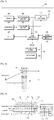
- FIGURE 2 illustrates an example eNB 102 according to this disclosure.
- the embodiment of the eNB 102 illustrated in FIGURE 2 is for illustration only, and the eNBs 101 and 103 of FIGURE 1 could have the same or similar configuration.
- eNBs come in a wide variety of configurations, and FIGURE 2 does not limit the scope of this disclosure to any particular implementation of an eNB.
- the eNB 102 includes multiple antennas 205a-205n, multiple RF transceivers 210a-210n, transmit (TX) processing circuitry 215, and receive (RX) processing circuitry 220.
- the eNB 102 also includes a controller/ processor 225, a memory 230, and a backhaul or network interface 235.
- the RF transceivers 210a-210n receive from the antennas 205a-205n incoming RF signals, such as signals transmitted by UEs in the wireless network 100.
- the RF transceivers 210a-210n down-convert the incoming RF signals to generate IF or baseband signals.
- the IF or baseband signals are sent to the RX processing circuitry 220, which generates processed baseband signals by filtering, decoding, and/or digitizing the baseband or IF signals.
- the RX processing circuitry 220 transmits the processed baseband signals to the controller/processor 225 for further processing.
- the TX processing circuitry 215 receives analog or digital data (such as voice data, web data, e-mail, or interactive video game data) from the controller/processor 225.
- the TX processing circuitry 215 encodes, multiplexes, and/or digitizes the outgoing baseband data to generate processed baseband or IF signals.
- the RF transceivers 210a-210n receive the outgoing processed baseband or IF signals from the TX processing circuitry 215 and up-converts the baseband or IF signals to RF signals that are transmitted via the antennas 205a-205n.
- the controller/processor 225 can include one or more processors or other processing devices that control the overall operation of the eNB 102.
- the controller/ processor 225 could control the reception of forward channel signals and the transmission of reverse channel signals by the RF transceivers 210a-210n, the RX processing circuitry 220, and the TX processing circuitry 215 in accordance with well-known principles.
- the controller/ processor 225 could support additional functions as well, such as more advanced wireless communication functions.
- the controller/processor 225 could support beam forming or directional routing operations in which outgoing signals from multiple antennas 205a-205n are weighted differently to effectively steer the outgoing signals in a desired direction. Any of a wide variety of other functions could be supported in the eNB 102 by the controller/processor 225.
- the controller/processor 225 includes at least one microprocessor or microcontroller.
- the controller/processor 225 is also capable of executing programs and other processes resident in the memory 230, such as a basic OS.
- the controller/processor 225 can move data into or out of the memory 230 as required by an executing process.
- the controller/processor 225 is also coupled to the backhaul or network interface 235.
- the backhaul or network interface 235 allows the eNB 102 to communicate with other devices or systems over a backhaul connection or over a network.
- the interface 235 could support communications over any suitable wired or wireless connection(s). For example, when the eNB 102 is implemented as part of a cellular communication system (such as one supporting 5G, LTE, or LTE-A), the interface 235 could allow the eNB 102 to communicate with other eNBs over a wired or wireless backhaul connection.
- the interface 235 could allow the eNB 102 to communicate over a wired or wireless local area network or over a wired or wireless connection to a larger network (such as the Internet).
- the interface 235 includes any suitable structure supporting communications over a wired or wireless connection, such as an Ethernet or RF transceiver.
- the memory 230 is coupled to the controller/processor 225. Part of the memory 230 could include a RAM, and another part of the memory 230 could include a Flash memory or other ROM.
- the eNB 102 could include one or more mixed-order bandpass FSS lenses.
- FIGURE 2 illustrates one example of eNB 102
- the eNB 102 could include any number of each component shown in FIGURE 2 .
- an access point could include a number of interfaces 235, and the controller/processor 225 could support routing functions to route data between different network addresses.
- the eNB 102 while shown as including a single instance of TX processing circuitry 215 and a single instance of RX processing circuitry 220, the eNB 102 could include multiple instances of each (such as one per RF transceiver).
- various components in FIGURE 2 could be combined, further subdivided, or omitted, and additional components could be added according to particular needs.
- FIGURE 3 illustrates an example UE 116 according to this disclosure.
- the embodiment of the UE 116 illustrated in FIGURE 3 is for illustration only, and the UEs 111-115 of FIGURE 1 could have the same or similar configuration.
- UEs come in a wide variety of configurations, and FIGURE 3 does not limit the scope of this disclosure to any particular implementation of a UE.
- the UE 116 includes an antenna 305, a radio frequency (RF) transceiver 310, transmit (TX) processing circuitry 315, a microphone 320, and receive (RX) processing circuitry 325.
- the UE 116 also includes a speaker 330, a main processor 340, an input/output (I/O) interface (IF) 345, a keypad 350, a display 355, and a memory 360.
- the memory 360 includes a basic operating system (OS) program 361 and one or more applications 362.
- OS basic operating system
- the RF transceiver 310 receives from the antenna 305 an incoming RF signal transmitted by an eNB of the network 100.
- the RF transceiver 310 down-converts the incoming RF signal to generate an intermediate frequency (IF) or baseband signal.
- the IF or baseband signal is sent to the RX processing circuitry 325, which generates a processed baseband signal by filtering, decoding, and/or digitizing the baseband or IF signal.
- the RX processing circuitry 325 transmits the processed baseband signal to the speaker 330 (such as for voice data) or to the main processor 340 for further processing (such as for web browsing data).
- the TX processing circuitry 315 receives analog or digital voice data from the microphone 320 or other outgoing baseband data (such as web data, e-mail, or interactive video game data) from the main processor 340.
- the TX processing circuitry 315 encodes, multiplexes, and/or digitizes the outgoing baseband data to generate a processed baseband or IF signal.
- the RF transceiver 310 receives the outgoing processed baseband or IF signal from the TX processing circuitry 315 and up-converts the baseband or IF signal to an RF signal that is transmitted via the antenna 305.
- the main processor 340 can include one or more processors or other processing devices and execute the basic OS program 361 stored in the memory 360 in order to control the overall operation of the UE 116.
- the main processor 340 could control the reception of forward channel signals and the transmission of reverse channel signals by the RF transceiver 310, the RX processing circuitry 325, and the TX processing circuitry 315 in accordance with well-known principles.
- the main processor 340 includes at least one microprocessor or microcontroller.
- the main processor 340 is also capable of executing other processes and programs resident in the memory 360.
- the main processor 340 can move data into or out of the memory 360 as required by an executing process.
- the main processor 340 is configured to execute the applications 362 based on the OS program 361 or in response to signals received from eNBs or an operator.
- the main processor 340 is also coupled to the I/O interface 345, which provides the UE 116 with the ability to connect to other devices, such as laptop computers and handheld computers.
- the I/O interface 345 is the communication path between these accessories and the main processor 340.
- the main processor 340 is also coupled to the keypad 350 and the display 355.
- the operator of the UE 116 can use the keypad 350 to enter data into the UE 116.
- the display 355 may be a liquid crystal display or other display capable of rendering text and/or at least limited graphics, such as from web sites.
- the memory 360 is coupled to the main processor 340.
- Part of the memory 360 could include a random access memory (RAM), and another part of the memory 360 could include a Flash memory or other read-only memory (ROM).
- RAM random access memory
- ROM read-only memory
- the UE 116 could include one or more mixed-order bandpass FSS lenses.
- FIGURE 3 illustrates one example of UE 116
- various changes may be made to FIGURE 3 .
- various components in FIGURE 3 could be combined, further subdivided, or omitted, and additional components could be added according to particular needs.
- the main processor 340 could be divided into multiple processors, such as one or more central processing units (CPUs) and one or more graphics processing units (GPUs).
- FIGURE 3 illustrates the UE 116 configured as a mobile telephone or smartphone, UEs could be configured to operate as other types of mobile or stationary devices.
- Embodiments of this disclosure recognize and take into account the fact that lenses may provide several significant improvements to antennas used in communication systems, including microwave and millimeter wave (MMW) communication systems. These improvements can include increased antenna directivity for specific point-to-point communications and improved link availability; increased antenna gains for better signal-to-noise ratios, data capacities, and link reliabilities; reduced antenna side-lobes for more effective use of antenna radiation patterns and for less interference from other radios; and reduced antenna losses for lower system power consumptions. Lenses provide these improvements while maintaining the capability of antenna pattern beam steering, which is useful in many microwave and MMW communication systems. Further, these enhancements can be realized using only passive structures to avoid the complexity and energy losses associated with approaches where active devices are used for such improvements.
- MMW millimeter wave
- Embodiments of this disclosure also recognize and take into account the fact that phase shifts realized by a frequency selective surface (FSS) can be used to design planar lenses.
- FSS frequency selective surface
- a wide range of phase shifts may be covered by tuning high-order bandpass FSSs.
- cascading multiple first-order FSSs with a spacing of a quarter wavelength between each panel can increase the overall thickness of the FSS and enhance the sensitivity of the frequency response to the angle and polarization of incidence of EM waves.
- Advances in FSS technology also enable the synthesis of low-profile high-order bandpass FSSs that are composed entirely of non-resonant periodic structures.
- One type of FSS uses a pair of inductive and capacitive layers to increase one or more orders of the bandpass response.
- this stacked topology with multiple bonding layers constitutes a bottleneck for commercial MMW applications due to its high cost and to performance degradations caused by multiple bonding layers.
- Embodiments of this disclosure further recognize and take into account the fact that certain planar lens technologies for microwave or MMW systems have critical drawbacks, which hamper their practical applications. These drawbacks can include the following:
- shortcomings in certain high-order bandpass FSS lenses may include the following:
- various embodiments of this disclosure provide low-cost, low-profile planar lenses.
- the lenses of this disclosure can be used in various ways, such as for gain/pattern enhancements of radiating elements (such as antennas) operating in wireless communication platforms like UEs and eNBs.
- various embodiments of this disclosure provide thinner configurations of planar lenses to cover elements with a reduced loading complexity.
- the lenses of various embodiments of this disclosure may enhance system gains at RF front ends without using active devices and thus improve signal-to-noise ratios (SNRs).
- SNRs signal-to-noise ratios
- the increase in the power level of a received signal may allow for a reduction of power consumption in the overall system and more reliable wireless connections.
- planar lenses employ a mixed-order bandpass filter response, which may allow for a reduction in the number of substrates and metal layers in the lenses while maintaining phase shift targets.
- the planar lenses of the present disclosure employ a single-substrate spatial mixed-order bandpass filter including one dielectric substrate and two metal layers. This approach allows for the reduction in the number of substrate and metal layers while maintaining desired goals for phase shift.
- some conventional lenses employ a third-order bandpass filter response, four substrates, five metal layers, and three bonding layers (where both inductive and capacitive layers are used).
- the single-substrate spatial mixed-order bandpass lens of the present disclosure uses one substrate and two metal layers and may not require bonding layers.
- FIGURE 4 illustrates an example planar FSS lens 400 in accordance with this disclosure.
- a phase shift is realized by the phase response of an FSS of the lens 400.
- An aperture of the lens 400 is split into multiple different zones (such as Zone1, Zone2, ..., ZoneN).
- Zone1, Zone2, ..., ZoneN zones
- rays passing through the different zones of the FSS experience different amounts of phase shift. More specifically, the phase shift experienced by rays passing through the lens 400 decreases the further the rays are from the center of the lens 400, so there are higher phase shifts near the center of the lens 400 and lower phase shifts near the edges of the lens 400.
- ⁇ diff
- the value of ⁇ diff is determined by the tunable range of the phase shift of FSS elements within the pass band of the FSS.
- the lens 400 may acquire the tunable range by modifying the sizes of the FSS elements slightly according to the number of zones.
- design parameters for the lens 400 include the size of the lens aperture (AP), the thickness (t) of the lens 400, and the size of FSS unit cells. As the aperture size increases, the focusing gain increases, but the focal length f also increases when ⁇ diff is fixed.
- the lens thickness is related to the sensitivity of the lens 400 to the angle of incidence of EM waves.
- smaller FSS unit cells lead to finer focusing resolutions of the lens 400 but can require better tolerances of a fabrication process.
- the aforementioned design parameters in the lens 400 may be determined by considering the tradeoffs among performance, size, and fabrication conditions.
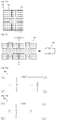
- FIGURE 5 illustrates an exploded view of an example topology of a mixed-order bandpass FSS lens 500 in accordance with this disclosure.
- the lens 500 includes a substrate layer 505 and two conductive element layers 510 and 515.
- the lens 500 is mixed-order in that the lens 500 includes a capacitively-loaded first-order bandpass FSS portion 520 and a second-order bandpass FSS portion 525.
- Portion 530 of layer 510 is enlarged to illustrate details of the patterns of conductive elements present in layer 510, which is described in greater detail below.
- FIGURES 6a and 6b illustrate perspective views of an example topology of a unit cell 600 for a second-order bandpass FSS in accordance with this disclosure.
- the unit cell 600 is an example of a unit cell present within a cross section of the second-order bandpass FSS portion 525 of the lens 500 in FIGURE 5 .
- the unit cell 600 is depicted in a side view, with a portion 605 of the substrate layer 505 present in the unit cell 600 depicted as being transparent so that the structure of a conductive element 610 in the conductive element layer 510 is viewable.
- the unit cell 600 is depicted in a top and/or bottom view, with the structure of the conductive element 610 and/or a conductive element 615 distinguished from the underlying portion 605 of the substrate layer 505.
- the unit cell 600 is a second-order bandpass FSS.
- the combination of a dielectric in the substrate portion 605 and metal in the conductive elements 610 and 615 provides a bandpass filter response for EM waves that propagate through the unit cell 600.
- Each side of the unit cell 600 provides a single-order bandpass FSS such that the unit cell 600 is a second-order bandpass FSS.
- Several such unit cells 600 form the second-order bandpass FSS portion 525 of the lens 500.
- the outer portions of the lens 500 may employ the second-order bandpass FSS. Different amounts of phase shifts and tuning of phase shifts may be obtainable by varying properties of the unit cell 600.
- These properties include, for example, the size of the conductive elements 610/615 in the conductive element layers 510/515, the thickness of the conductive elements 610/615 in the conductive element layers 510/515, g1 (the size(s) of the gap between adjacent conductive elements 610/615 in a conductive element layer 510/515), g2 (the size(s) of the gaps within the conductive elements 610/615), L (the length between gaps on opposite ends of the conductive element), w (the width between gaps on the same end of the conductive element), and/or other properties of the structure of the conductive elements 610/615 in the unit cell 600.
- the structure of the conductive elements 610 and 615 shown in FIGURES 6a and 6b is for the purpose of illustrating one example of a second-order bandpass FSS.
- Other suitable structure shapes may be utilized (such as rectangles, triangles, and ellipses). Additionally, any number of different sizes, positions, and number of gaps within the conductive elements 610/615 may be suitably employed in accordance with the principles of the present disclosure.
- FIGURES 7a through 7c illustrate perspective views of an example topology of a unit cell 700 for a capacitively-loaded, first-order bandpass FSS in accordance with this disclosure.
- the unit cell 700 is an example of a unit cell present within a cross section of the capacitively-loaded, first-order bandpass FSS portion 520 of the lens 500 in FIGURE 5 .
- the unit cell 700 is depicted in a side view, with a portion 705 of the substrate layer 505 present in the unit cell 700 depicted as transparent so that the structure of conductive elements 710 in the conductive element layer 510 is viewable.
- the unit cell 700 is depicted from one side 720 (such as a top and/or bottom view), with the structure of the conductive elements 710 distinguished from the underlying portion 705 of the substrate layer 505.
- the unit cell 700 is depicted from the other side 725 (such as a bottom and/or top side), with the structure of conductive elements 715 again distinguished from the underlying portion 705 of the substrate layer 505.
- the conductive elements 710/715 have the same structure as the conductive elements 610/615 in the unit cell 600.
- the unit cell 700 is a capacitively-loaded, first-order bandpass FSS.
- the combination of a dielectric in the substrate portion 705 and metal in the conductive elements 710 provides a capacitive filter response for EM waves that propagate through the side 720 of the unit cell 700.
- the structure of the conductive elements may have a patch structure, such as a rectangular shape, which provides the capacitive filter response for EM waves that propagate through the side 720 of the unit cell 700.
- the combination of the dielectric in the substrate portion 705 and metal in the conductive elements 715 provides a bandpass filter response for EM waves that propagate through the side 725 of the unit cell 700.
- the unit cell 700 is a first-order bandpass FSS that is "capacitively loaded.”
- unit cells 700 form the capacitively-loaded, first-order bandpass FSS portion 520 of the lens 500.
- the inner portions of the lens 500 may employ the capacitively-loaded, first-order bandpass FSS.
- Different amounts of phase shifts and tuning of phase shifts may be obtainable by varying properties of the unit cell 700.
- these properties include, for example, size, thickness, g1, g2, L, w, and/or other properties of the structure of the conductive elements 710/715 in the unit cell 700.
- the side 720 includes the property g3, which refers to the size(s) of the gap between adjacent conductive elements 710 in the side 720 and/or in the portion 525 of the layer 510 of the lens 500.
- the illustrations of the unit cells 600 and 700 are examples only and for the purpose of showing the structure and arrangement of individual conductive elements within their respective layers.
- the lens 500 includes multiple unit cells, and the substrate layer 505 is substantially contiguous or unbroken across the multiple unit cells.
- FIGURE 8 illustrates an example topology and equivalent circuit model of a bandpass FSS 800 in accordance with this disclosure.
- the FSS 800 may be a portion of either side of the lens 500 having a bandpass filter metal layer structure, such as the layer 515 or the portions of the layer 510 in the second-order portion 525.
- the combination of the dielectric in the substrate layer 505 and the metal in the conductive element layer(s) 510 and/or 515 provides a bandpass filter response for EM waves that propagate through the bandpass FSS 800.
- a circuit model 805 illustrates a shunt resonator including a shunt inductor and shunt capacitor realized on a single surface including conductive elements and dielectric gaps.
- FIGURES 9a and 9b illustrate equivalent circuit models for an example second-order bandpass FSS and an example capacitively-loaded, first-order bandpass FSS, respectively, of an FSS lens in accordance with this disclosure.
- a circuit model 900 shows the circuit equivalence of the phase shift obtained by EM waves that propagate through the second-order bandpass FSS bandpass portions of an FSS lens, such as the portion 525 in the lens 500.
- the model 900 includes two bandpass filter responses (a capacitor in parallel with an inductor).
- a circuit model 905 shows the circuit equivalence of the phase shift obtained by EM waves that propagate through a capacitively-loaded, first-order bandpass FSS, such as the portion 520 in the lens 500.
- the model 905 includes one bandpass filter response (a capacitor in parallel with an inductor) on one side, with the other side having a capacitive filter response.
- the circuit models 900 and 905 are for the purpose of illustrating an equivalent or approximate representation of the phase shift properties of the different portions of the FSS lens 500.
- the capacitive loading in the capacitively-loaded first-order bandpass FSS lowers the overall phase shift values for the portion 520 of the FSS lens 500 at the operating frequency of the lens 500.
- the capacitive loading can allow the portion 520 of the FSS lens 500 to cover a new tunable range of phase shifts that may not be covered by a bandpass-only spatial FSS.
- the tunable range of phase shifts for different-order bandpass spatial FSSs may overlap.
- a mixed-order bandpass-only FSS may not provide additional tunable ranges of phase shifts beyond that of the highest order in the bandpass FSS.
- the tunable range of phase shifts for first- and second-order bandpass FSSs may be encompassed within the tunable range of phase shifts for a third-order bandpass FSS.
- the capacitive loading of the portion 520 of the FSS lens 500 modifies the slope of the lower cutoff frequency response, which moves the tunable range of phase shifts for the capacitively-loaded, first-order FSS portion 520 of the FSS lens 500 to cover a range that may not be covered by the second-order bandpass FSS portion 525 of the FSS lens 500.
- the capacitively-loaded first- and second-order FSS lens of the present disclosure may provide a tunable range of phase shifts comparable to that of a third-order bandpass filter, which is unexpected for bandpass filters.
- the use of a single substrate, while providing a comparable tunable range of phase shifts as a third-order bandpass FSS lens (which may need multiple substrates and bonding layers), provides several advantages as described herein.
- FIGURES 10a and 10b illustrate example magnitude and phase plots, respectively, of transmittance of a mixed-order bandpass FSS lens in accordance with this disclosure.
- FIGURE 10a illustrates a plot 1000 of the magnitude response of different portions of the FSS lens 500.
- FIGURE 10b illustrates a plot 1005 of the frequency response of different portions of the FSS lens 500.
- the phase response for the first-order portions of the FSS lens 500 does not overlap the phase response for the second-order portions of the FSS lens 500.
- a tunable range 1010 of the mixed-order FSS lens 500 is increased.
- the tunable range 1010 of the FSS lens 500 may be about 200°.
- This tunable range may be greater than some third-order bandpass FSS lenses, which may employ much larger numbers of metal, substrate, and/or bonding layers. Accordingly, the mixed-order bandpass FSS lens 500 can achieve desired goals of attaining suitable phase shift tunable ranges while reducing the size, thickness, and/or machining limitations of existing lenses.
- the lens 500 can represent a single-substrate mixed-order bandpass FSS lens designed for a 28.2GHz operating frequency with a unit cell size of 2.7mm, and the dielectric constant and thickness of the substrates (Rogers 3003) are 3mm and 0.5mm, respectively.
- the lens 500 provides sub-wavelength filtering.
- the size or lateral dimension of the conductive elements and the overall thickness of the lens may be less than a wavelength of the operating frequency designed for spatial phase shifting by the lens 500.
- design parameters (such as g1, g2, g3, w, and L) are appropriately tuned for the second-order and capacitively-loaded first-order bandpass portions.
- Values for the design parameters of the FSS lens 500 for the 28.2GHz design example are listed in the legend for the plots 1000 and 1005.
- the values and dimensions described above are examples only and are not limitations on different dimensions that may be utilized in accordance with embodiments of this disclosure.
- the sizes, number, and/or gaps of the conductive elements in any of the layers may be increased or decreased based on various factors, such as phase shifts, lens thicknesses, and/or machining tolerances.
- the mixed-order bandpass FSS lens 500 of the present disclosure may utilize fewer metal and dielectric layers than that of existing planar lenses while providing comparable or better ranges of spatial phase shifts.
- First-order capacitively-loaded elements may be placed in the center of the FSS lens 500, while second-order elements may be placed around the outside of the lens.
- the higher absolute phase delay of the first-order capacitively-loaded elements is utilized in the central portion of the lens 500 to provide a larger phase delay for collimation or focusing EM waves near the center of the lens.
- the second-order elements towards the outer region of the lens 500 provide less absolute phase delay but contribute to a wider range of phase delay for tuning the collimation or focusing of the planar lens 500.
- advantages of using the mixed-order bandpass FSS lens of this disclosure may include:
- the FSS lenses can enhance coverage of a beam steering angle.
- an FSS lens may include spatial phase shifters that cause waves propagating through the lens to be focused in any desired angle.
- the FSS lenses may be utilized for beam broadening. This beam broadening can provide different levels of beam widths in different angles of radiation, which can enable multi-functional wireless communications (such as antenna diversity).
- the FSS lenses of this disclosure can be used with any type or shape of antennas, such as horn antennas, monopole antennas, dipole antennas, and slot antennas. Additionally, while the shape of the FSS lens is illustrated in some of the figures as being flat, the FSS lens may be a curved, non-flat, and/or conformal lens. Also, while the use of metal for the conductive elements has been described, the conductive elements could be fabricated from other conductive material(s). Moreover, while the shape of the conductive elements is illustrated in some of the figures as being rectangular or square, the conductive elements may have other shapes.
- the conductive elements may be hexagons, ellipses, circles, octagons, shapes with curved as well as straight edges, etc.
- the FSS lenses of this disclosure can be designed and fabricated for applications involving nearly any RF frequency range, from a few megahertz to multiple hundreds of gigahertz (such as 1 MHz to 300 GHz).
- the planar lenses of this disclosure can be fabricated and integrated with various platforms without strict fabrication process requirements. For instance, patterns in the planar lenses of this disclosure may only be two dimensional without requiring vertical structures.
- Embodiments of this disclosure provide several significant improvements to antennas for wireless communication systems and other applications.
- the FSS lenses of this disclosure can provide increased antenna gains and directivities, reduced antenna pattern side-lobes, and reduced antenna losses. These technical improvements provide a host of commercial and market advantages to any products and systems using such lenses.
- the FSS lenses of this disclosure can provide higher data throughputs or higher data capacities.
- the higher antenna gains of antennas with lenses produce higher signal-to-noise ratio values, and higher signal-to-noise ratio values provide higher data throughputs and higher data capacities.
- the FSS lenses of this disclosure can provide better connection availabilities and better connection establishments.
- the FSS lenses can provide higher gains and stronger signals, and stronger signal levels between eNBs and UEs (or between other devices) provide more dependable initial establishment of connection between the devices.
- the FSS lenses of this disclosure can also provide more reliable wireless connections due to higher directivities and higher interference suppressions of antennas with lenses. Higher directivities of beam steering provide alignment of antenna patterns with communication paths or channels. Higher directivities and lower side-lobes also reduce the level of undesired signals intercepted along a desired communication path.
- the FSS lenses of this disclosure can further provide lower densities of eNBs with a greater range of UEs. The higher antenna gains allow UEs to operate farther from their eNBs with comparable transmitter powers, allowing fewer eNBs within a given area.
- the FSS lenses of this disclosure can provide longer battery life for mobile or consumer products.
- the enhanced gain of a mobile antenna allows a reduction in transmitter power for comparable signal level.
- the improved gain of an eNB antenna provides a reduction in the power required for the receiver at a UE.
- the enhanced gain can reduce the electrical power consumed in the UE's electronics and allow longer operations between battery recharge cycles.
- the FSS lenses of this disclosure can also provide smaller products or products with more features and functions.
- the enhanced antenna directivities or gains provided allow the area used by the antenna to be reduced. The extra area may be re-allocated for components needed for other system functions or features, or the extra area may be used to reduce the overall size and volume of a UE or eNB.
Landscapes
- Aerials With Secondary Devices (AREA)
Claims (14)
- Appareil comprenant:une lentille (400) comprenant une pluralité de couches d'éléments conducteurs (610, 615, 710, 715) et une couche de substrat (505) ;une première des couches d'éléments conducteurs (610, 615, 710, 715) comprenant une première partie (520) comprenant des éléments conducteurs (610, 615, 715) possédant une première structure et une seconde partie (525) comprenant des éléments conducteurs (710) possédant une seconde structure différente de la première structure, caractérisé en ce que :
la lentille (400) est une surface sélective en fréquence d'ordre mixte (FSS), comprenant :une partie centrale qui comprend des éléments conducteurs de structures différentes sur des côtés opposés de la couche de substrat (505) ;et une partie externe qui comprend des éléments conducteurs possédant un même type de structure sur la couche de substrat (505). - Appareil selon la revendication 1,
ladite première des couches étant en contact avec un côté de la couche de substrat (505) ;
et des éléments conducteurs (610, 615, 710, 715) dans une seconde des couches d'éléments conducteurs (610, 615, 710, 715) étant en contact avec un autre côté de la couche de substrat (505) et possédant la première structure. - Appareil selon la revendication 2, une taille et une épaisseur des éléments conducteurs (610, 615, 715) possédant la première structure variant sur la seconde couche d'éléments conducteurs (610, 615, 710, 715).
- Appareil selon la revendication 1, ladite partie centrale (400) comprenant un premier type de cellule unitaire (700) comprenant :au moins un élément conducteur (715) possédant la première structure positionnée sur un côté de la couche de substrat (505) ;et des éléments conducteurs (710) possédant la seconde structure positionnée sur un autre côté de la couche de substrat (505).
- Appareil selon la revendication 4, ledit premier type de cellule unitaire (700) étant conçu pour fournir une réponse de filtre passe-bande à charge capacitive pour des ondes électromagnétiques traversant le premier type de cellule unitaire (700).
- Appareil selon la revendication 5,
ladite partie externe (400) comprenant un second type de cellule unitaire (600) comprenant des éléments conducteurs (610, 615) positionnés sur des côtés opposés de la couche de substrat (505) et possédant la première structure ;
et ledit second type de cellule unitaire (600) étant conçu pour fournir une réponse de filtre passe-bande pour les ondes électromagnétiques traversant le second type de cellule unitaire (600). - Appareil selon la revendication 1, une taille et une épaisseur des éléments conducteurs (610, 615, 710, 715) possédant la première structure et la seconde structure variant sur la première des couches d'éléments conducteurs (610, 615, 710, 715).
- Appareil selon la revendication 1,
ladite première structure étant une structure de filtre passe-bande ;
et ladite seconde structure étant une structure de plaque. - Appareil selon la revendication 1, une plage de réponses de déphasage pour les ondes électromagnétiques traversant la lentille (400) étant basée sur au moins un espacement entre les éléments conducteurs (610, 615, 710, 715) dans la pluralité de couches.
- Appareil selon la revendication 1, ladite lentille (400) comprenant uniquement deux couches d'éléments conducteurs (610, 615, 710, 715) et une couche de substrat (505).
- Appareil selon la revendication 1, une dimension latérale des éléments conducteurs (610, 615, 710, 715) et une épaisseur de la lentille (400) étant inférieures à une longueur d'onde d'une fréquence de fonctionnement pour un déphasage spatial.
- Procédé comprenant :
l'émission d'ondes électromagnétiques à travers une lentille (400) comprenant une pluralité de couches d'éléments conducteurs (610, 615, 710, 715) et une couche de substrat (505), une première des couches d'éléments conducteurs (610, 615, 710, 715) comprenant une première partie (520) comprenant des éléments conducteurs (610, 615, 710, 715) possédant une première structure et une seconde partie (525) comprenant des éléments conducteurs (710) possédant une seconde structure différente de la première structure, caractérisé en ce que :
la lentille (400) est une surface sélective en fréquence d'ordre mixte (FSS), comprenant :une partie centrale qui comprend des éléments conducteurs de structures différentes sur des côtés opposés de la couche de substrat (505) ;et une partie externe qui comprend des éléments conducteurs possédant un même type de structure sur la couche de substrat (505). - Procédé selon la revendication 12,
ladite première des couches étant en contact avec un côté de la couche de substrat (505) ;
et des éléments conducteurs (610, 615, 710, 715) dans une seconde des couches d'éléments conducteurs (610, 615, 710, 715) étant en contact avec un autre côté de la couche de substrat (505) et possédant la première structure. - Procédé selon la revendication 13, ladite partie centrale (400) comprenant un premier type de cellule unitaire (700) comprenant :au moins un élément conducteur (715) possédant la première structure positionnée sur un côté de la couche de substrat (505) ;et des éléments conducteurs (710) possédant la seconde structure positionnée sur un autre côté de la couche de substrat (505).
Applications Claiming Priority (3)
| Application Number | Priority Date | Filing Date | Title |
|---|---|---|---|
| US201361843749P | 2013-07-08 | 2013-07-08 | |
| US14/293,985 US9425513B2 (en) | 2013-07-08 | 2014-06-02 | Lens with spatial mixed-order bandpass filter |
| PCT/KR2014/009847 WO2015186867A1 (fr) | 2013-07-08 | 2014-10-20 | Lentille avec filtre spatial passe-bande d'ordre mixte |
Publications (3)
| Publication Number | Publication Date |
|---|---|
| EP3149540A1 EP3149540A1 (fr) | 2017-04-05 |
| EP3149540A4 EP3149540A4 (fr) | 2018-01-24 |
| EP3149540B1 true EP3149540B1 (fr) | 2019-12-04 |
Family
ID=52132431
Family Applications (1)
| Application Number | Title | Priority Date | Filing Date |
|---|---|---|---|
| EP14893861.6A Active EP3149540B1 (fr) | 2013-07-08 | 2014-10-20 | Lentille avec filtre spatial passe-bande d'ordre mixte |
Country Status (4)
| Country | Link |
|---|---|
| US (1) | US9425513B2 (fr) |
| EP (1) | EP3149540B1 (fr) |
| CN (1) | CN106415369B (fr) |
| WO (1) | WO2015186867A1 (fr) |
Families Citing this family (16)
| Publication number | Priority date | Publication date | Assignee | Title |
|---|---|---|---|---|
| US10116058B2 (en) | 2015-02-13 | 2018-10-30 | Samsung Electronics Co., Ltd. | Multi-aperture planar lens antenna system |
| KR102391485B1 (ko) | 2016-03-17 | 2022-04-28 | 삼성전자주식회사 | 무선 통신 시스템에서 빔을 송신하기 위한 방법 및 장치 |
| JP2018191247A (ja) * | 2017-05-11 | 2018-11-29 | 日本電信電話株式会社 | 電磁界バンドパスフィルタ |
| KR102380185B1 (ko) | 2017-09-18 | 2022-03-29 | 삼성전자주식회사 | 무선 통신 시스템에서 빔포밍을 운용하기 위한 장치 및 방법 |
| KR102531003B1 (ko) | 2017-12-19 | 2023-05-10 | 삼성전자 주식회사 | 렌즈를 포함하는 빔포밍 안테나 모듈 |
| KR102486588B1 (ko) | 2017-12-19 | 2023-01-10 | 삼성전자 주식회사 | 렌즈를 포함하는 빔포밍 안테나 모듈 |
| KR102529946B1 (ko) | 2017-12-19 | 2023-05-08 | 삼성전자 주식회사 | 렌즈를 포함하는 빔포밍 안테나 모듈 |
| KR20190118794A (ko) | 2018-04-11 | 2019-10-21 | 삼성전자주식회사 | 무선 통신 시스템에서 렌즈를 이용하여 빔을 조절하기 위한 장치 및 방법 |
| KR20190118792A (ko) | 2018-04-11 | 2019-10-21 | 삼성전자주식회사 | 무선 통신 시스템에서 렌즈를 이용하여 빔을 제어하기 위한 장치 및 방법 |
| KR102482247B1 (ko) | 2018-08-13 | 2022-12-28 | 삼성전자주식회사 | 평면 렌즈를 포함하는 안테나 장치 |
| US11705637B2 (en) * | 2018-10-11 | 2023-07-18 | Northeastern University | Magnetodielectric metamaterials and articles including magnetodielectric metamaterials |
| CN109802242B (zh) * | 2019-03-05 | 2020-12-11 | 南京理工大学 | 超表面透镜 |
| CN110943278B (zh) * | 2019-10-29 | 2021-06-25 | Oppo广东移动通信有限公司 | 阵列透镜、透镜天线和电子设备 |
| CN110739552B (zh) * | 2019-10-31 | 2021-10-22 | Oppo广东移动通信有限公司 | 透镜结构、透镜天线及电子设备 |
| CN111262035B (zh) * | 2020-01-17 | 2021-04-20 | 安徽捷纳森电子科技有限公司 | 基于频率选择表面的屏蔽材料 |
| FR3126003B1 (fr) | 2021-08-09 | 2025-03-07 | Arkema France | Polyamide de rigidité élevée à sorption d’eau réduite |
Family Cites Families (24)
| Publication number | Priority date | Publication date | Assignee | Title |
|---|---|---|---|---|
| US2849713A (en) | 1955-12-01 | 1958-08-26 | Scientific Atlanta | Spherical microwave lens |
| US4721966A (en) | 1986-05-02 | 1988-01-26 | The United States Of America As Represented By The Secretary Of The Air Force | Planar three-dimensional constrained lens for wide-angle scanning |
| US5373302A (en) * | 1992-06-24 | 1994-12-13 | The United States Of America As Represented By The Administrator Of The National Aeronautics And Space Administration | Double-loop frequency selective surfaces for multi frequency division multiplexing in a dual reflector antenna |
| US5455594A (en) * | 1992-07-16 | 1995-10-03 | Conductus, Inc. | Internal thermal isolation layer for array antenna |
| US5497169A (en) * | 1993-07-15 | 1996-03-05 | The United States Of America As Represented By The Administrator Of The National Aeronautics And Space Administration | Wide angle, single screen, gridded square-loop frequency selective surface for diplexing two closely separated frequency bands |
| JP3257383B2 (ja) | 1996-01-18 | 2002-02-18 | 株式会社村田製作所 | 誘電体レンズ装置 |
| US6606077B2 (en) * | 1999-11-18 | 2003-08-12 | Automotive Systems Laboratory, Inc. | Multi-beam antenna |
| WO2002031914A1 (fr) | 2000-10-12 | 2002-04-18 | E-Tenna Corporation | Antennes dielectriques artificielles accordables de poids reduit |
| US6396451B1 (en) * | 2001-05-17 | 2002-05-28 | Trw Inc. | Precision multi-layer grids fabrication technique |
| US7071889B2 (en) * | 2001-08-06 | 2006-07-04 | Actiontec Electronics, Inc. | Low frequency enhanced frequency selective surface technology and applications |
| US6822622B2 (en) * | 2002-07-29 | 2004-11-23 | Ball Aerospace & Technologies Corp | Electronically reconfigurable microwave lens and shutter using cascaded frequency selective surfaces and polyimide macro-electro-mechanical systems |
| WO2004020186A2 (fr) | 2002-08-29 | 2004-03-11 | The Regents Of The University Of California | Materiaux indefinis |
| US7420524B2 (en) * | 2003-04-11 | 2008-09-02 | The Penn State Research Foundation | Pixelized frequency selective surfaces for reconfigurable artificial magnetically conducting ground planes |
| US7145418B2 (en) | 2004-12-15 | 2006-12-05 | Raytheon Company | Bandpass filter |
| US7898480B2 (en) * | 2005-05-05 | 2011-03-01 | Automotive Systems Labortaory, Inc. | Antenna |
| US7821473B2 (en) | 2007-05-15 | 2010-10-26 | Toyota Motor Engineering & Manufacturing North America, Inc. | Gradient index lens for microwave radiation |
| US20090058746A1 (en) * | 2007-08-31 | 2009-03-05 | Harris Corporation | Evanescent wave-coupled frequency selective surface |
| TWI398984B (zh) | 2008-05-23 | 2013-06-11 | Murata Manufacturing Co | Laminated bandpass filter |
| US8421706B2 (en) | 2009-02-27 | 2013-04-16 | Toyota Motor Engineering & Manufacturing North America, Inc. | Metamaterial microwave lens |
| US8633866B2 (en) | 2010-02-26 | 2014-01-21 | The Regents Of The University Of Michigan | Frequency-selective surface (FSS) structures |
| US8228251B1 (en) | 2010-08-23 | 2012-07-24 | University Of Central Florida Research Foundation, Inc. | Ultra-wideband, low profile antenna |
| JP4766354B1 (ja) | 2010-09-09 | 2011-09-07 | Tdk株式会社 | 積層型バンドパスフィルタ |
| US8811511B2 (en) * | 2010-09-28 | 2014-08-19 | Wisconsin Alumni Research Foundation | Hybrid analog-digital phased MIMO transceiver system |
| US8912973B2 (en) | 2011-05-04 | 2014-12-16 | The Penn State Research Foundation | Anisotropic metamaterial gain-enhancing lens for antenna applications |
-
2014
- 2014-06-02 US US14/293,985 patent/US9425513B2/en not_active Expired - Fee Related
- 2014-10-20 CN CN201480079526.1A patent/CN106415369B/zh not_active Expired - Fee Related
- 2014-10-20 WO PCT/KR2014/009847 patent/WO2015186867A1/fr not_active Ceased
- 2014-10-20 EP EP14893861.6A patent/EP3149540B1/fr active Active
Non-Patent Citations (1)
| Title |
|---|
| None * |
Also Published As
| Publication number | Publication date |
|---|---|
| EP3149540A4 (fr) | 2018-01-24 |
| WO2015186867A1 (fr) | 2015-12-10 |
| US9425513B2 (en) | 2016-08-23 |
| CN106415369A (zh) | 2017-02-15 |
| US20150009080A1 (en) | 2015-01-08 |
| EP3149540A1 (fr) | 2017-04-05 |
| CN106415369B (zh) | 2019-08-02 |
Similar Documents
| Publication | Publication Date | Title |
|---|---|---|
| EP3149540B1 (fr) | Lentille avec filtre spatial passe-bande d'ordre mixte | |
| US20140313090A1 (en) | Lens with mixed-order cauer/elliptic frequency selective surface | |
| US11552397B2 (en) | High gain and large bandwidth antenna incorporating a built-in differential feeding scheme | |
| EP3857643B1 (fr) | Antenne avec métamatériau à gradient d'indice | |
| US9742070B2 (en) | Open end antenna, antenna array, and related system and method | |
| US20150200452A1 (en) | Planar beam steerable lens antenna system using non-uniform feed array | |
| JP6446547B2 (ja) | ワイヤレス電子デバイスのための周期スロットを有するストリップライン結合アンテナ | |
| Rahmati et al. | Multiband metallic frequency selective surface with wide range of band ratio | |
| US11063344B2 (en) | High gain and large bandwidth antenna incorporating a built-in differential feeding scheme | |
| EP3987614B1 (fr) | Antennes réseau à ondes millimétriques à double bande et à double polarisation ayant un niveau de lobe latéral (sll) amélioré pour des terminaux 5g | |
| US20150194736A1 (en) | Quasi-yagi-type antenna | |
| Guo et al. | Antenna technologies for 6G–Advances and challenges | |
| CN114256636B (zh) | 具有多个相控天线阵列的电子设备 | |
| Hassan et al. | Designs strategies and performance of IoT antennas: a comprehensive review | |
| EP3020091A1 (fr) | Techniques pour commander des antennes réseaux à commande de phase dans des modules radio à onde millimétrique | |
| US11258187B2 (en) | Antenna array for wide angle beam steering | |
| KR20230067692A (ko) | 안테나 디바이스, 안테나 디바이스들의 어레이 | |
| EP4340123A1 (fr) | Architecture de réseau d'antennes compacte et à large bande à commutation de faisceau | |
| CN112018497A (zh) | 天线模组及电子设备 | |
| CN109904592B (zh) | 一种天线结构及通信终端 | |
| Sharma et al. | 4-port MIMO antenna backed with frequency selective surface (FSS) for improved characteristics in n46 and n47 WLAN Bands | |
| KR102173843B1 (ko) | 공간 혼합-차수 대역통과 필터를 갖는 렌즈 | |
| Volakis et al. | Highlights of Antenna Innovations (1974–2024): New developments over recent decades | |
| So et al. | Multiband sector antenna with the same beamwidth employing multiple woodpile metamaterial reflectors | |
| US11522270B2 (en) | Solution for beam tilting associated with dual-polarized mm-Wave antennas in 5G terminals |
Legal Events
| Date | Code | Title | Description |
|---|---|---|---|
| STAA | Information on the status of an ep patent application or granted ep patent |
Free format text: STATUS: THE INTERNATIONAL PUBLICATION HAS BEEN MADE |
|
| PUAI | Public reference made under article 153(3) epc to a published international application that has entered the european phase |
Free format text: ORIGINAL CODE: 0009012 |
|
| STAA | Information on the status of an ep patent application or granted ep patent |
Free format text: STATUS: REQUEST FOR EXAMINATION WAS MADE |
|
| 17P | Request for examination filed |
Effective date: 20161208 |
|
| AK | Designated contracting states |
Kind code of ref document: A1 Designated state(s): AL AT BE BG CH CY CZ DE DK EE ES FI FR GB GR HR HU IE IS IT LI LT LU LV MC MK MT NL NO PL PT RO RS SE SI SK SM TR |
|
| AX | Request for extension of the european patent |
Extension state: BA ME |
|
| DAX | Request for extension of the european patent (deleted) | ||
| A4 | Supplementary search report drawn up and despatched |
Effective date: 20171221 |
|
| RIC1 | Information provided on ipc code assigned before grant |
Ipc: H01Q 15/10 20060101ALI20171215BHEP Ipc: H01Q 19/06 20060101AFI20171215BHEP |
|
| REG | Reference to a national code |
Ref country code: DE Ref legal event code: R079 Ref document number: 602014058075 Country of ref document: DE Free format text: PREVIOUS MAIN CLASS: G02B0027460000 Ipc: H01Q0019060000 |
|
| GRAP | Despatch of communication of intention to grant a patent |
Free format text: ORIGINAL CODE: EPIDOSNIGR1 |
|
| STAA | Information on the status of an ep patent application or granted ep patent |
Free format text: STATUS: GRANT OF PATENT IS INTENDED |
|
| RIC1 | Information provided on ipc code assigned before grant |
Ipc: H01Q 15/10 20060101ALI20190731BHEP Ipc: H01Q 19/06 20060101AFI20190731BHEP |
|
| GRAS | Grant fee paid |
Free format text: ORIGINAL CODE: EPIDOSNIGR3 |
|
| INTG | Intention to grant announced |
Effective date: 20190902 |
|
| GRAA | (expected) grant |
Free format text: ORIGINAL CODE: 0009210 |
|
| STAA | Information on the status of an ep patent application or granted ep patent |
Free format text: STATUS: THE PATENT HAS BEEN GRANTED |
|
| AK | Designated contracting states |
Kind code of ref document: B1 Designated state(s): AL AT BE BG CH CY CZ DE DK EE ES FI FR GB GR HR HU IE IS IT LI LT LU LV MC MK MT NL NO PL PT RO RS SE SI SK SM TR |
|
| REG | Reference to a national code |
Ref country code: GB Ref legal event code: FG4D |
|
| REG | Reference to a national code |
Ref country code: CH Ref legal event code: EP |
|
| REG | Reference to a national code |
Ref country code: AT Ref legal event code: REF Ref document number: 1210576 Country of ref document: AT Kind code of ref document: T Effective date: 20191215 |
|
| REG | Reference to a national code |
Ref country code: DE Ref legal event code: R096 Ref document number: 602014058075 Country of ref document: DE |
|
| REG | Reference to a national code |
Ref country code: IE Ref legal event code: FG4D |
|
| REG | Reference to a national code |
Ref country code: NL Ref legal event code: MP Effective date: 20191204 |
|
| REG | Reference to a national code |
Ref country code: LT Ref legal event code: MG4D |
|
| PG25 | Lapsed in a contracting state [announced via postgrant information from national office to epo] |
Ref country code: LT Free format text: LAPSE BECAUSE OF FAILURE TO SUBMIT A TRANSLATION OF THE DESCRIPTION OR TO PAY THE FEE WITHIN THE PRESCRIBED TIME-LIMIT Effective date: 20191204 Ref country code: NO Free format text: LAPSE BECAUSE OF FAILURE TO SUBMIT A TRANSLATION OF THE DESCRIPTION OR TO PAY THE FEE WITHIN THE PRESCRIBED TIME-LIMIT Effective date: 20200304 Ref country code: GR Free format text: LAPSE BECAUSE OF FAILURE TO SUBMIT A TRANSLATION OF THE DESCRIPTION OR TO PAY THE FEE WITHIN THE PRESCRIBED TIME-LIMIT Effective date: 20200305 Ref country code: FI Free format text: LAPSE BECAUSE OF FAILURE TO SUBMIT A TRANSLATION OF THE DESCRIPTION OR TO PAY THE FEE WITHIN THE PRESCRIBED TIME-LIMIT Effective date: 20191204 Ref country code: SE Free format text: LAPSE BECAUSE OF FAILURE TO SUBMIT A TRANSLATION OF THE DESCRIPTION OR TO PAY THE FEE WITHIN THE PRESCRIBED TIME-LIMIT Effective date: 20191204 Ref country code: BG Free format text: LAPSE BECAUSE OF FAILURE TO SUBMIT A TRANSLATION OF THE DESCRIPTION OR TO PAY THE FEE WITHIN THE PRESCRIBED TIME-LIMIT Effective date: 20200304 Ref country code: LV Free format text: LAPSE BECAUSE OF FAILURE TO SUBMIT A TRANSLATION OF THE DESCRIPTION OR TO PAY THE FEE WITHIN THE PRESCRIBED TIME-LIMIT Effective date: 20191204 |
|
| PG25 | Lapsed in a contracting state [announced via postgrant information from national office to epo] |
Ref country code: RS Free format text: LAPSE BECAUSE OF FAILURE TO SUBMIT A TRANSLATION OF THE DESCRIPTION OR TO PAY THE FEE WITHIN THE PRESCRIBED TIME-LIMIT Effective date: 20191204 Ref country code: HR Free format text: LAPSE BECAUSE OF FAILURE TO SUBMIT A TRANSLATION OF THE DESCRIPTION OR TO PAY THE FEE WITHIN THE PRESCRIBED TIME-LIMIT Effective date: 20191204 |
|
| PG25 | Lapsed in a contracting state [announced via postgrant information from national office to epo] |
Ref country code: AL Free format text: LAPSE BECAUSE OF FAILURE TO SUBMIT A TRANSLATION OF THE DESCRIPTION OR TO PAY THE FEE WITHIN THE PRESCRIBED TIME-LIMIT Effective date: 20191204 |
|
| PG25 | Lapsed in a contracting state [announced via postgrant information from national office to epo] |
Ref country code: PT Free format text: LAPSE BECAUSE OF FAILURE TO SUBMIT A TRANSLATION OF THE DESCRIPTION OR TO PAY THE FEE WITHIN THE PRESCRIBED TIME-LIMIT Effective date: 20200429 Ref country code: ES Free format text: LAPSE BECAUSE OF FAILURE TO SUBMIT A TRANSLATION OF THE DESCRIPTION OR TO PAY THE FEE WITHIN THE PRESCRIBED TIME-LIMIT Effective date: 20191204 Ref country code: CZ Free format text: LAPSE BECAUSE OF FAILURE TO SUBMIT A TRANSLATION OF THE DESCRIPTION OR TO PAY THE FEE WITHIN THE PRESCRIBED TIME-LIMIT Effective date: 20191204 Ref country code: EE Free format text: LAPSE BECAUSE OF FAILURE TO SUBMIT A TRANSLATION OF THE DESCRIPTION OR TO PAY THE FEE WITHIN THE PRESCRIBED TIME-LIMIT Effective date: 20191204 Ref country code: NL Free format text: LAPSE BECAUSE OF FAILURE TO SUBMIT A TRANSLATION OF THE DESCRIPTION OR TO PAY THE FEE WITHIN THE PRESCRIBED TIME-LIMIT Effective date: 20191204 Ref country code: RO Free format text: LAPSE BECAUSE OF FAILURE TO SUBMIT A TRANSLATION OF THE DESCRIPTION OR TO PAY THE FEE WITHIN THE PRESCRIBED TIME-LIMIT Effective date: 20191204 |
|
| PG25 | Lapsed in a contracting state [announced via postgrant information from national office to epo] |
Ref country code: SK Free format text: LAPSE BECAUSE OF FAILURE TO SUBMIT A TRANSLATION OF THE DESCRIPTION OR TO PAY THE FEE WITHIN THE PRESCRIBED TIME-LIMIT Effective date: 20191204 Ref country code: IS Free format text: LAPSE BECAUSE OF FAILURE TO SUBMIT A TRANSLATION OF THE DESCRIPTION OR TO PAY THE FEE WITHIN THE PRESCRIBED TIME-LIMIT Effective date: 20200404 Ref country code: SM Free format text: LAPSE BECAUSE OF FAILURE TO SUBMIT A TRANSLATION OF THE DESCRIPTION OR TO PAY THE FEE WITHIN THE PRESCRIBED TIME-LIMIT Effective date: 20191204 |
|
| REG | Reference to a national code |
Ref country code: DE Ref legal event code: R097 Ref document number: 602014058075 Country of ref document: DE |
|
| REG | Reference to a national code |
Ref country code: AT Ref legal event code: MK05 Ref document number: 1210576 Country of ref document: AT Kind code of ref document: T Effective date: 20191204 |
|
| PLBE | No opposition filed within time limit |
Free format text: ORIGINAL CODE: 0009261 |
|
| STAA | Information on the status of an ep patent application or granted ep patent |
Free format text: STATUS: NO OPPOSITION FILED WITHIN TIME LIMIT |
|
| PG25 | Lapsed in a contracting state [announced via postgrant information from national office to epo] |
Ref country code: DK Free format text: LAPSE BECAUSE OF FAILURE TO SUBMIT A TRANSLATION OF THE DESCRIPTION OR TO PAY THE FEE WITHIN THE PRESCRIBED TIME-LIMIT Effective date: 20191204 |
|
| PGFP | Annual fee paid to national office [announced via postgrant information from national office to epo] |
Ref country code: GB Payment date: 20200923 Year of fee payment: 7 |
|
| 26N | No opposition filed |
Effective date: 20200907 |
|
| PG25 | Lapsed in a contracting state [announced via postgrant information from national office to epo] |
Ref country code: AT Free format text: LAPSE BECAUSE OF FAILURE TO SUBMIT A TRANSLATION OF THE DESCRIPTION OR TO PAY THE FEE WITHIN THE PRESCRIBED TIME-LIMIT Effective date: 20191204 Ref country code: PL Free format text: LAPSE BECAUSE OF FAILURE TO SUBMIT A TRANSLATION OF THE DESCRIPTION OR TO PAY THE FEE WITHIN THE PRESCRIBED TIME-LIMIT Effective date: 20191204 Ref country code: SI Free format text: LAPSE BECAUSE OF FAILURE TO SUBMIT A TRANSLATION OF THE DESCRIPTION OR TO PAY THE FEE WITHIN THE PRESCRIBED TIME-LIMIT Effective date: 20191204 |
|
| PG25 | Lapsed in a contracting state [announced via postgrant information from national office to epo] |
Ref country code: IT Free format text: LAPSE BECAUSE OF FAILURE TO SUBMIT A TRANSLATION OF THE DESCRIPTION OR TO PAY THE FEE WITHIN THE PRESCRIBED TIME-LIMIT Effective date: 20191204 |
|
| PGFP | Annual fee paid to national office [announced via postgrant information from national office to epo] |
Ref country code: DE Payment date: 20200921 Year of fee payment: 7 |
|
| REG | Reference to a national code |
Ref country code: CH Ref legal event code: PL |
|
| PG25 | Lapsed in a contracting state [announced via postgrant information from national office to epo] |
Ref country code: LU Free format text: LAPSE BECAUSE OF NON-PAYMENT OF DUE FEES Effective date: 20201020 Ref country code: MC Free format text: LAPSE BECAUSE OF FAILURE TO SUBMIT A TRANSLATION OF THE DESCRIPTION OR TO PAY THE FEE WITHIN THE PRESCRIBED TIME-LIMIT Effective date: 20191204 |
|
| REG | Reference to a national code |
Ref country code: BE Ref legal event code: MM Effective date: 20201031 |
|
| PG25 | Lapsed in a contracting state [announced via postgrant information from national office to epo] |
Ref country code: FR Free format text: LAPSE BECAUSE OF NON-PAYMENT OF DUE FEES Effective date: 20201031 |
|
| PG25 | Lapsed in a contracting state [announced via postgrant information from national office to epo] |
Ref country code: CH Free format text: LAPSE BECAUSE OF NON-PAYMENT OF DUE FEES Effective date: 20201031 Ref country code: BE Free format text: LAPSE BECAUSE OF NON-PAYMENT OF DUE FEES Effective date: 20201031 Ref country code: LI Free format text: LAPSE BECAUSE OF NON-PAYMENT OF DUE FEES Effective date: 20201031 |
|
| PG25 | Lapsed in a contracting state [announced via postgrant information from national office to epo] |
Ref country code: IE Free format text: LAPSE BECAUSE OF NON-PAYMENT OF DUE FEES Effective date: 20201020 |
|
| REG | Reference to a national code |
Ref country code: DE Ref legal event code: R119 Ref document number: 602014058075 Country of ref document: DE |
|
| PG25 | Lapsed in a contracting state [announced via postgrant information from national office to epo] |
Ref country code: TR Free format text: LAPSE BECAUSE OF FAILURE TO SUBMIT A TRANSLATION OF THE DESCRIPTION OR TO PAY THE FEE WITHIN THE PRESCRIBED TIME-LIMIT Effective date: 20191204 Ref country code: MT Free format text: LAPSE BECAUSE OF FAILURE TO SUBMIT A TRANSLATION OF THE DESCRIPTION OR TO PAY THE FEE WITHIN THE PRESCRIBED TIME-LIMIT Effective date: 20191204 Ref country code: CY Free format text: LAPSE BECAUSE OF FAILURE TO SUBMIT A TRANSLATION OF THE DESCRIPTION OR TO PAY THE FEE WITHIN THE PRESCRIBED TIME-LIMIT Effective date: 20191204 |
|
| GBPC | Gb: european patent ceased through non-payment of renewal fee |
Effective date: 20211020 |
|
| PG25 | Lapsed in a contracting state [announced via postgrant information from national office to epo] |
Ref country code: MK Free format text: LAPSE BECAUSE OF FAILURE TO SUBMIT A TRANSLATION OF THE DESCRIPTION OR TO PAY THE FEE WITHIN THE PRESCRIBED TIME-LIMIT Effective date: 20191204 |
|
| PG25 | Lapsed in a contracting state [announced via postgrant information from national office to epo] |
Ref country code: GB Free format text: LAPSE BECAUSE OF NON-PAYMENT OF DUE FEES Effective date: 20211020 Ref country code: DE Free format text: LAPSE BECAUSE OF NON-PAYMENT OF DUE FEES Effective date: 20220503 |