EP3149848B1 - Oszillatorschaltung mit vorstromgenerator - Google Patents
Oszillatorschaltung mit vorstromgenerator Download PDFInfo
- Publication number
- EP3149848B1 EP3149848B1 EP14730799.5A EP14730799A EP3149848B1 EP 3149848 B1 EP3149848 B1 EP 3149848B1 EP 14730799 A EP14730799 A EP 14730799A EP 3149848 B1 EP3149848 B1 EP 3149848B1
- Authority
- EP
- European Patent Office
- Prior art keywords
- bias current
- increasing
- level
- signal
- generating
- Prior art date
- Legal status (The legal status is an assumption and is not a legal conclusion. Google has not performed a legal analysis and makes no representation as to the accuracy of the status listed.)
- Active
Links
Images


Classifications
-
- H—ELECTRICITY
- H03—ELECTRONIC CIRCUITRY
- H03L—AUTOMATIC CONTROL, STARTING, SYNCHRONISATION OR STABILISATION OF GENERATORS OF ELECTRONIC OSCILLATIONS OR PULSES
- H03L3/00—Starting of generators
-
- H—ELECTRICITY
- H03—ELECTRONIC CIRCUITRY
- H03B—GENERATION OF OSCILLATIONS, DIRECTLY OR BY FREQUENCY-CHANGING, BY CIRCUITS EMPLOYING ACTIVE ELEMENTS WHICH OPERATE IN A NON-SWITCHING MANNER; GENERATION OF NOISE BY SUCH CIRCUITS
- H03B5/00—Generation of oscillations using amplifier with regenerative feedback from output to input
- H03B5/30—Generation of oscillations using amplifier with regenerative feedback from output to input with frequency-determining element being electromechanical resonator
- H03B5/32—Generation of oscillations using amplifier with regenerative feedback from output to input with frequency-determining element being electromechanical resonator being a piezoelectric resonator
-
- H—ELECTRICITY
- H03—ELECTRONIC CIRCUITRY
- H03K—PULSE TECHNIQUE
- H03K19/00—Logic circuits, i.e. having at least two inputs acting on one output; Inverting circuits
- H03K19/20—Logic circuits, i.e. having at least two inputs acting on one output; Inverting circuits characterised by logic function, e.g. AND, OR, NOR, NOT circuits
-
- H—ELECTRICITY
- H03—ELECTRONIC CIRCUITRY
- H03L—AUTOMATIC CONTROL, STARTING, SYNCHRONISATION OR STABILISATION OF GENERATORS OF ELECTRONIC OSCILLATIONS OR PULSES
- H03L5/00—Automatic control of voltage, current, or power
-
- H—ELECTRICITY
- H03—ELECTRONIC CIRCUITRY
- H03B—GENERATION OF OSCILLATIONS, DIRECTLY OR BY FREQUENCY-CHANGING, BY CIRCUITS EMPLOYING ACTIVE ELEMENTS WHICH OPERATE IN A NON-SWITCHING MANNER; GENERATION OF NOISE BY SUCH CIRCUITS
- H03B2200/00—Indexing scheme relating to details of oscillators covered by H03B
- H03B2200/0002—Types of oscillators
- H03B2200/0012—Pierce oscillator
-
- H—ELECTRICITY
- H03—ELECTRONIC CIRCUITRY
- H03B—GENERATION OF OSCILLATIONS, DIRECTLY OR BY FREQUENCY-CHANGING, BY CIRCUITS EMPLOYING ACTIVE ELEMENTS WHICH OPERATE IN A NON-SWITCHING MANNER; GENERATION OF NOISE BY SUCH CIRCUITS
- H03B2200/00—Indexing scheme relating to details of oscillators covered by H03B
- H03B2200/006—Functional aspects of oscillators
- H03B2200/0062—Bias and operating point
-
- H—ELECTRICITY
- H03—ELECTRONIC CIRCUITRY
- H03B—GENERATION OF OSCILLATIONS, DIRECTLY OR BY FREQUENCY-CHANGING, BY CIRCUITS EMPLOYING ACTIVE ELEMENTS WHICH OPERATE IN A NON-SWITCHING MANNER; GENERATION OF NOISE BY SUCH CIRCUITS
- H03B2200/00—Indexing scheme relating to details of oscillators covered by H03B
- H03B2200/006—Functional aspects of oscillators
- H03B2200/0066—Amplitude or AM detection
-
- H—ELECTRICITY
- H03—ELECTRONIC CIRCUITRY
- H03B—GENERATION OF OSCILLATIONS, DIRECTLY OR BY FREQUENCY-CHANGING, BY CIRCUITS EMPLOYING ACTIVE ELEMENTS WHICH OPERATE IN A NON-SWITCHING MANNER; GENERATION OF NOISE BY SUCH CIRCUITS
- H03B2200/00—Indexing scheme relating to details of oscillators covered by H03B
- H03B2200/006—Functional aspects of oscillators
- H03B2200/0082—Lowering the supply voltage and saving power
-
- H—ELECTRICITY
- H03—ELECTRONIC CIRCUITRY
- H03B—GENERATION OF OSCILLATIONS, DIRECTLY OR BY FREQUENCY-CHANGING, BY CIRCUITS EMPLOYING ACTIVE ELEMENTS WHICH OPERATE IN A NON-SWITCHING MANNER; GENERATION OF NOISE BY SUCH CIRCUITS
- H03B2200/00—Indexing scheme relating to details of oscillators covered by H03B
- H03B2200/006—Functional aspects of oscillators
- H03B2200/0094—Measures to ensure starting of oscillations
Definitions
- the present disclosure relates to an oscillator circuit, a method of operating an oscillator circuit, and a wireless communication device comprising an oscillator circuit.
- a system clock is typically generated using a crystal oscillator.
- a crystal oscillator comprises an active part and a resonator.
- the active part comprises an amplifier and is commonly referred to as the oscillator core.
- the resonator which comprises a piezoelectric crystal, is coupled between an input of the active part and an output of the active part.
- the oscillator core may be integrated with a transceiver in an integrated circuit, the crystal being external to the integrated circuit, or the oscillator core and crystal may be implemented in a module, such as a temperature controlled crystal oscillator (TCXO), external to a transceiver integrated circuit.
- TXO temperature controlled crystal oscillator
- the negative resistance of the oscillator core should be arranged to ensure oscillator start-up, negative resistance being the property whereby a voltage decreases in response to an increasing current, but integrated circuit process variation can result in a spread in the negative resistance of the oscillator core.
- US2012/068774A1 discloses an amplitude control circuit that includes a pair of peak detectors.
- the pair of peak detectors are responsive to a voltage reference generator.
- the amplitude control circuit is configured to be responsive to an oscillating signal of a crystal oscillator and configured to generate a control signal to control an amplitude of the oscillating signal.
- US2012/154066A1 discloses an oscillator that includes a reference voltage generator, an oscillation element configured to oscillate by either a drive voltage or a drive current and output an oscillation signal, a peak hold element configured to detect a peak level of the oscillation signal for output; and a controller configured to increase or decrease the drive voltage or drive current in accordance with the reference voltage generated by the reference voltage generator and the peak level output from the peak hold element.
- EP2634914A1 discloses an oscillator circuit comprising first and second resonator terminals for connecting to respective terminals of a resonator.
- the oscillator circuit also comprises a first inverting amplifier connected between the first and second resonator terminals in a first mode of operation; and a back to back pair of second inverting amplifiers connected between the first and second resonator terminals in a second mode of operation.
- a controller configured to compare an operational parameter of the oscillator circuit to a switchover threshold, and switch the oscillator circuit from the first mode of operation to the second mode of operation when the operational parameter exceeds the switchover threshold.
- US6798301 B1 discloses a circuit which controls an oscillation amplitude of a crystal oscillator including a crystal resonator, a current source supplying a bias current, and an output transistor coupled to the crystal resonator and the current source.
- the circuit includes a peak detector for detecting a peak voltage of an output signal of the crystal oscillator, and a controller coupled to the peak detector and to the current source for controlling the current source in accordance with a difference between the peak voltage and a target voltage, the target voltage being set to be substantially equal to 2Vth, where Vth is a threshold voltage of the output transistor.
- a frequency control circuit controls a first switched-capacitor array and a second switched-capacitor array coupled to the crystal resonator, and alternately switches a unit capacitor in the first switched-capacitor array and a unit capacitor in the second switched-capacitor array based on a frequency control signal.
- EP0724331A1 discloses a semiconductor integrated circuit having a constant voltage generation circuit and an oscillation circuit for generating a clock signal.
- the constant voltage generation circuit supplies a first voltage to the oscillation circuit until the clock signal is stabilized and the constant voltage generation circuit supplies a second voltage lower than the first voltage to the oscillation circuit after the clock signal has been stabilized.
- US2007/096841A1 discloses a frequency source having a fast start-up time and low noise in steady state.
- the frequency source includes an oscillator and a hybrid automatic gain control (AGC) loop that switches between an analog AGC loop at oscillator start up and a digital AGC loop at steady state operation.
- the analog AGC loop includes a peak detector connected to the oscillator and an error integrator integrating the difference between the peak detector output and a reference voltage.
- the digital AGC loop includes a comparator comparing the peak detector output and high/low reference voltages, an oscillator counter providing a timer signal, a digital-to-analog converter (DAC) supplied with a digital word, and a low pass filter between the DAC and the oscillator.
- the timer signal causes a multiplexer to select either the analog AGC loop or the digital AGC loop.
- JP2006121477A discloses an oscillation device that is provided with an inverter for inputting the output amplitude of a crystal oscillation circuit, and for changing an output pulse width according to the change of the output amplitude, and configured to detect the amplitude of the oscillation signal of the crystal oscillation circuit by monitoring the change of the pulse width (duty rate) of a pulse signal outputted from the inverter, and to detect the amplitude of the oscillation signal of the crystal oscillation circuit, and to control the driving voltage VOSC of the crystal oscillation circuit so that the output amplitude of the crystal oscillation circuit can be put in a state immediately before it is saturated based on the detection result.
- WO8903617A1 discloses a signal source for generating a well-controlled, predictable oscillating output signal within a short, predetermined and constant start-up time.
- the invention includes a switchable current source for selectively providing an electrical signal to a tank circuit which, in response, provides an oscillating output signal.
- a control circuit comprising a comparator is connected to the tank circuit for providing a control signal to the switchable current source which causes the current source to switch in response to the output signal.
- Particular embodiments of the invention include means for controlling the amplitude of the oscillating output signal, means for controlling the transconductance of the current source, and means for starting the signal source.
- a wireless communication device comprising the oscillator circuit of the first aspect.
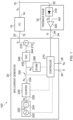
- a first preferred embodiment of an oscillator circuit 100 comprises a crystal oscillator (XO) 10, a bias current generator 20 and a feedback stage 30.
- the crystal oscillator 10 has an input 12 coupled to an output 22 of the bias current generator 20 for receiving a bias current is generated by the bias current generator 20, and an output 14 coupled to an output 15 of the oscillator circuit 100 for delivering an oscillation signal S O .
- the feedback stage 30 has an input 32 coupled to the output 14 of the crystal oscillator 10 for receiving the oscillation signal S O , and an output 34 for delivering a feedback signal S F .
- the feedback stage 30 comprises an amplitude detector 310 coupled to the input 32 of the feedback stage 30.
- the amplitude detector 310 generates an indication S A of the amplitude of the oscillation signal S O .
- the feedback stage 30 also comprises a comparator 320 coupled to the amplitude detector 310 for receiving the indication S A of the amplitude of the oscillation signal S O .
- the comparator 320 is also coupled to an amplitude threshold REF.
- the comparator 320 When the oscillator circuit 100 is powered-up, and consequently the amplitude of the oscillation signal S O increases from zero, the comparator 320 generates a feedback signal S F in response to the amplitude of the oscillation signal S O , and therefore the indication S A , reaching the amplitude threshold REF.
- the comparator 320 is coupled to the output 34 of the feedback stage 30 for delivering the feedback signal S F .
- the output 34 of the feedback stage 30 is coupled to a first input 24 of the bias current generator 20.
- the bias current generator 20 has a second input 26 for an initialisation signal S I , and a third input 28 for a wake-up signal S W .
- the initialisation signal S I indicates to the oscillator circuit 100 when the oscillator circuit 100 is required to commence oscillation from an initial power-off state, when initialisation is required, and the wake-up signal S W indicates when the oscillator circuit 100 is required to commence oscillation from a subsequent power-off state, when initialisation is not required again. Power supply connections to the oscillator circuit 100 are not illustrated in Figure 1 , for clarity.
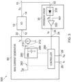
- the bias current generator 20 comprises a current source 210 coupled to the output 22 of the bias current generator 20 for generating the bias current I B .
- the current source 210 has a control input 212 for controlling the magnitude of the bias current, as described below.
- the bias current generator 20 comprises an auxiliary clock signal generator 220 that generates an auxiliary clock signal S C .
- the auxiliary clock signal generator 220 comprises an auxiliary oscillator 222 that generates an auxiliary oscillation signal S X , coupled to a frequency divider 224 that generates the auxiliary clock signal S C by dividing the auxiliary oscillation signal S X .
- the frequency divider 224 may have a division ratio of, for example, one hundred, with the auxiliary oscillation signal S X having a frequency of, for example, 100kHz and the auxiliary clock signal S C having a frequency of 1kHz.
- An output 226 of the auxiliary clock signal generator 220 is coupled to a counter 230 that generates a count value N C by counting pulses, that is, cycles, of the auxiliary clock signal S C . Therefore, the count value N C increases in a step-wise manner.
- the frequency divider 224 may be omitted, in which case the output 226 of the auxiliary clock signal generator 220 corresponds to an output of the auxiliary oscillator 222, and is coupled to the counter 230.
- the auxiliary oscillation signal S X is used as the auxiliary clock signal S C
- the auxiliary clock signal S C has a frequency equal to a frequency of the auxiliary oscillation signal S X , for example 1kHz.
- An output 234 of the counter 230 is coupled to an input 242 of a digital-to-analogue (DAC) converter 240 via a switch 250.
- a storage device (STORE) 260 is coupled to the input 242 of the DAC 240, and therefore is also coupled to the to the output 234 of the counter 230 via the switch 250.
- the switch 250 In a first state of the switch 250, in which the switch 250 is closed, that is, is in a conducting state, the count value N C is delivered from the output 234 of the counter 230 to the input 242 of the DAC 240, and to the storage device 260 for storing the current count value N C . This stored value is denoted N S .
- the output 234 of the counter 230 is de-coupled from the input 242 of the DAC 240, and from the storage device 260, and in this state the stored value N S , instead of the increasing count value N C , is delivered to the input 242 of the DAC 240. Therefore, depending on the state of the switch 250, the storage device 260 is arranged to either store a new count value N C , or to output the stored value N S , as described in detail below.
- An output 244 of the DAC 240 is coupled to the control input 212 of the current source 210 for controlling the magnitude of the bias current I B dependent on the increasing count value N C delivered at the output 234 of the counter 230, or the stored value N S which is constant, according to the state of the switch 250.
- the bias current generator 20 also comprises a controller 270 coupled to the first, second and third inputs 24, 26, 28 of the bias current generator 20 for receiving, respectively, the feedback signal S F , the initialisation signal S I and the wake-up signal S W .
- the controller 270 is also coupled to the auxiliary oscillator 220 for starting and stopping generation of the auxiliary clock signal S C , to the counter 230 for starting and resetting the counting of the pulses of the auxiliary clock signal S C , to the switch 250 for controlling whether the switch 250 has the first state or the second state, and to the storage device 260 for initiating storage of the current count value N C into the storage device 260 and reading of the stored value N S from the storage device 260.
- step 400 power is switched on, thereby supplying power to the oscillator circuit 100.
- This power-on condition is detected in the oscillator circuit 100 by means of the initialisation signal S I at the second input 26 of the bias current generator 20, which is supplied to the controller 270.
- the controller 270 In response to the initialisation signal S I , at step 410 the controller 270 initialises the count value N C of the counter 230 to zero, sets the switch 250 into the first state, thereby enabling the count value N C to be routed to the DAC 240, and then enables the auxiliary oscillator 220 to start generating the auxiliary clock signal S C .
- the bias current I B With the count value N C initialised to zero, the bias current I B has a first level that is zero or near zero, being insufficient to sustain oscillation of the crystal oscillator 10 for the expected spread of crystal resistance and the expected spread of negative resistance of the active part.
- the counter 230 increments in response to receiving a pulse of the auxiliary clock signal S C from the auxiliary oscillator 220, thereby increasing the count value N C , and consequently increasing the bias current I B supplied to the crystal oscillator 10.
- the count value N C increments in a step-wise manner, smoothing may take place in the current source 210 such that the bias current I B increases in a more gradual manner.
- the amplitude detector 310 detects the amplitude of the oscillation signal S O and generates the indication S A of the amplitude of the oscillation signal S O . This amplitude will be zero if the crystal oscillator 10 has not yet started to oscillate.
- the comparator 320 compares the indication S A with the amplitude reference REF. If the indication S A is less than the amplitude reference REF, the feedback signal S F is not generated at the output 34 of the feedback stage 30, and flow returns to step 420 where the counter 230 again increments in response to receiving a further pulse of the auxiliary clock signal S C from the auxiliary oscillator 220, thereby further increasing the count value N C , and consequently further increasing the bias current I B supplied to the crystal oscillator 10.
- the loop comprising steps 420, 430 and 440 is repeated, thereby successively increasing the bias current I B with each iteration. While the count value N C is low, the bias current I B may be insufficient to sustain oscillation of the crystal oscillator 10.
- the bias current I B increases to a level sufficient to sustain oscillation of the crystal oscillator 10. As the count value N C increases further, the bias current I B increases further, thereby enabling the amplitude of the oscillation signal S O to increase.
- step 440 If, at step 440, the comparator 320 determines that the indication S A is equal to, or greater than, the amplitude reference REF, flow proceeds to step 450 where the feedback signal S F is generated at the output 34 of the feedback stage 30. Flow then proceeds to step 460.
- the controller 270 in response to the feedback signal S F , the controller 270 enables the storage device 260 to store the current count value N C , that is N S , and sets the switch 250 into the second state, thereby enabling the stored value N S to be routed to the DAC 240. Consequently, for subsequent oscillation, the bias current I B becomes constant at a second level dependent on the stored value N S . Also at step 460, the controller 270 may disable the auxiliary oscillator 220 and the counter 230 in order to conserve power.
- the rate of increase of the count value N C depends on the frequency of the auxiliary clock signal S C , and this frequency may be selected to ensure that the rate of increase of the amplitude of the oscillation signal S O is sufficiently slow to avoid generation of unwanted parasitic oscillations.
- the oscillation signal S O has a frequency of 26MHz and the frequency of the auxiliary clock signal S C is 1kHz, the oscillation signal S O will have 26000 cycles for each increment of the count value N C and each increment of the bias current I B . If, on average, 8 increments are required before the feedback signal S F is generated, the start-up time will on average be about 8ms.
- the auxiliary clock signal S C preferably has a frequency lower than the frequency of the oscillation signal S O , for example not exceeding one tenth, or not exceeding one hundredth, or not exceeding one thousandth of the frequency of the oscillation signal S O .
- the rate of increase of the amplitude of the oscillation signal S O depends on the characteristics of the crystal oscillator 10, and in particular on the resistance of the crystal employed by the crystal oscillator 10 and on the negative resistance of the oscillator core. Therefore the stored value N S will also depend on these factors, and is adapted by the oscillator circuit 100 dependent on these factors.
- the level of the bias current I B may be established dependent on the stored value N S , without requiring to perform the initialisation process of increasing the bias current I B in response to the increasing count value N C . Therefore, subsequent start-up of the oscillator circuit 100 may be faster than the start-up when the initialisation process is performed.
- the storage device 260 should be non-volatile, retaining the stored value N S while power is switched off.
- the initialisation process may be performed when power to the oscillator circuit 100 is switched from off to on, for example during manufacture of the oscillator circuit 100 or manufacture of a device comprising the oscillator circuit 100, or when a user of a device comprising the oscillator circuit 100 initiates powering-on by pushing a power-on button.
- initialisation is not required and the level of the bias current I B may be established dependent on the stored value N S .
- such a wake-up may be performed within 1ms.
- the storage device 260 and the switch 250 may be omitted and, under the control of the controller 270, the counter 230 may cease counting and retain the final count value N C reached, with this final count value N C being delivered to the input 242 of the DAC 240 for subsequent oscillation of the crystal oscillator 10.
- This variant is suitable in circumstances where, for example, the initialisation is performed every time the oscillator circuit 100 is powered-up and the time required to perform the initialisation on each such occasion is tolerable.
- the stored value N S may be different from the final count value N C , and in particular may be lower than the final count value N C by a predetermined amount, for example by a single increment. This variant may be employed in circumstances where the amplitude of the oscillation signal S O may overshoot a desired maximum value during the increasing of the bias current I B due to the count value N C being quantised.
- the bias current I B supplied during subsequent operation of the crystal oscillator 10, and which is dependent on the stored value N S may be lower than the final level of the bias current I B reached when the increasing is terminated, thereby ensuring the amplitude of the oscillation signal S O does not exceed the desired maximum, but nevertheless is dependent on this final level. More generally, during subsequent operation of the crystal oscillator 10, that is, after the initialisation process, the bias current I B is supplied at a second level dependent on, and optionally but not necessarily equal to, the final level of the bias current I B reached when the increasing of the bias current I B is terminated.
- the bias current I B may be at a third level dependent on the stored value N S , the third level being optionally but not necessarily equal to the final level of the bias current I B reached when the increasing of the bias current I B is terminated during the initialisation process.
- the second and third levels may be equal.
- a second preferred embodiment of an oscillator circuit 500 comprises the crystal oscillator 10 and the feedback stage 30 as described with reference to Figure 1 coupled to a bias current generator 50 that has the same inputs and outputs as the bias current generator 20 described with reference to Figure 1 , but a different internal architecture. Therefore, the description in the following paragraphs of the oscillator circuit 500 is focussed principally on the internal architecture of the bias current generator 50. The crystal oscillator 10 and the feedback stage 30 and their connections are not described again.
- the bias current generator 50 comprises an integrator 280 coupled to a power supply voltage V dd via a switch 282.
- the integrator 280 is illustrated as a simple resistor-capacitor (RC) network, but other integration circuits may alternatively be used.
- the integrator 280 In response to the switch 282 closing, the integrator 280 generates an increasing ramp voltage V R at an output 284 of the integrator 280.
- the bias current generator 50 also comprises the current source 210, and the output 284 of the integrator 280 is coupled to the control input 212 of the current source 210 which therefore generates the bias current I B having a level, that is, magnitude, dependent on the ramp voltage V R . Therefore, the bias current I B increases as the ramp voltage V R at the control input 212 of the current source 210 increases.
- the bias current generator 50 also comprises a controller 290 coupled to the first, second and third inputs 24, 26, 28 of the bias current generator 50 for receiving, respectively, the feedback signal S F , the initialisation signal S I and the wake-up signal S W .
- the controller 290 is also coupled to the switch 282 for controlling the starting and stopping of the generation of the ramp voltage V R , and to the integrator 280 for resetting any voltage stored in the integrator 280 to zero or a low value.
- the controller 290 resets the voltage stored in the integrator 280 and closes the switch 282.
- the voltage stored in the integrator 280 starts to increase, thereby providing the ramp voltage V R , and consequently the bias current I B starts to increase in level from a first level which may be zero or small, being insufficient to sustain oscillation of the crystal oscillator 10.
- the controller 280 opens the switch 282. Consequently, the ramp voltage V R stops increasing, and the final level reached by the ramp voltage V R is stored in the integrator 280, thereby causing the bias current I B to cease increasing and become constant at a second level, corresponding to the final level of the ramp voltage V R .
- the level of the bias current I B is constant at the second level, being dependent on the voltage stored in the integrator 280.
- the rate of increase of the bias current I B while the ramp voltage V R is increasing, and consequently the rate of increase of the amplitude of the oscillation signal S O depends on the integration time constant of the integrator 280, and this time constant may be selected to be sufficiently slow to avoid generation of unwanted parasitic oscillations.
- a wireless communication device 300 comprises an antenna 310 coupled to an input of a low noise amplifier 320 for amplifying an RF signal received by the antenna 310.
- An output of the low noise amplifier 320 is coupled to a first input 332 of a down-conversion stage 330 for down-converting the amplified RF signal to baseband by mixing the amplified RF signal with quadrature related components of a local oscillator signal present at a second input 334 of the down-conversion stage 330.
- the baseband signal comprises quadrature related components.
- An output 336 of the down-conversion stage 330 is coupled to an input 352 of a digital signal processor (DSP) 350 via an analogue-to-digital converter (ADC) 340 that digitises the quadrature related components of the baseband signal.
- the DSP 350 demodulates and decodes the digitised baseband signal.
- the DSP 350 also generates, at an output 354 of the DSP 350, quadrature related components of a baseband signal for up-conversion.
- the output 354 of the DSP 350 is coupled to a first input 372 of an up-conversion stage 370 via a DAC 360.
- the up-conversion stage 370 up-converts the baseband signal to RF for transmission by mixing the quadrature related components of the baseband signal with quadrature related components of the local oscillator signal present at a second input 374 of the up-conversion stage 370.
- An output 376 of the up-conversion stage 370 is coupled to the antenna 310 via a power amplifier 380 that amplifies the RF signal for transmission.
- the wireless communication device 300 comprises the oscillator circuit 100, or alternatively may comprise the oscillator circuit 500.
- the output 15 of the oscillator circuit 100 is coupled to an input 392 of a phase shifting element 390.
- the phase shifting element 390 generates from the oscillation signal S O quadrature related components of the local oscillator signal at both a first output 394 and also at a second output 396 of the phase shifting element 390.
- the first output 394 of the phase shifting element 390 is coupled to the second input 334 of the down-conversion stage 330 for delivering the quadrature related components of a local oscillator signal to the down-conversion stage 330
- the second output 396 of the phase shifting element 390 is coupled to the second input 374 of the up-conversion stage 370 for delivering the quadrature related components of the local oscillator signal present to the up-conversion stage 370.
- these stored values may be updated by repeating the initialisation process. Moreover, these stored values may be updated by an automatic gain control (AGC) scheme in response to fluctuations in the amplitude of the oscillation signal S O , in order to restore the amplitude of the oscillation signal S O to a target level. Nonetheless, such updated values remain dependent on the final level of the bias current I B reached when the increasing of the level of the bias current I B is terminated.
- AGC automatic gain control
Landscapes
- Physics & Mathematics (AREA)
- Engineering & Computer Science (AREA)
- Computer Hardware Design (AREA)
- Computing Systems (AREA)
- General Engineering & Computer Science (AREA)
- Mathematical Physics (AREA)
- Oscillators With Electromechanical Resonators (AREA)
Claims (12)
- Verfahren zum Betreiben einer Oszillatorschaltung (100), umfassend:
als Reaktion darauf, dass eine Stromzufuhr an die Oszillatorschaltung (100) eingeschaltet wird, Initialisieren der Oszillatorschaltung, wobei das Initialisieren der Oszillatorschaltung Folgendes umfasst:Generieren eines Vorstroms mit einem steigenden Pegel, der bei einem ersten Pegel beginnt;Zuführen des Vorstroms an einen Kristalloszillator (10);Generieren eines Rückkopplungssignals als Reaktion darauf, dass eine Amplitude eines Oszillationssignals, das durch den Kristalloszillator (10) generiert wird, eine Amplitudenschwelle erreicht; undals Reaktion auf das Rückkopplungssignal, Beenden des Steigerns und Speichern einer Anzeige des finalen Pegels des Vorstroms, der erreicht wurde, wenn das Steigern beendet wird; undwährend nachfolgendem Betrieb des Kristalloszillators (10), Zuführen des Vorstroms auf einem zweiten Pegel in Abhängigkeit von dem finalen Pegel des Vorstroms, der erreicht wurde, wenn das Steigern beendet wird,wobei das Verfahren ferner Folgendes umfasst:
als Reaktion darauf, dass die Stromzufuhr an die Oszillatorschaltung (100) nach einem Zwischenzeitraum des Betriebs in einem Ruhemodus, in dem die Stromzufuhr an die Oszillatorschaltung abgeschaltet ist, eingeschaltet wird, Generieren des Vorstroms auf einem dritten Pegel in Abhängigkeit von der gespeicherten Anzeige, ohne erneutes Initialisieren der Oszillatorschaltung. - Verfahren nach einem der vorhergehenden Ansprüche, wobei der zweite Pegel gleich dem finalen Pegel ist.
- Verfahren nach Anspruch 1 oder Anspruch 2, wobei das Generieren des Vorstroms mit einem steigenden Pegel Folgendes umfasst:Generieren einer steigenden Sägezahnspannung; undSteigern des Pegels des Vorstroms als Reaktion auf die steigende Sägezahnspannung.
- Verfahren zum Betreiben einer Oszillatorschaltung (100) nach Anspruch 1, wobei das Generieren des Vorstroms mit einem steigenden Pegel Folgendes umfasst:Generieren eines Hilfstaktsignals;Generieren eines steigenden Zählwerts durch Zählen von Impulsen des Hilfstaktsignals; undSteigern des Pegels des Vorstroms als Reaktion auf den steigenden Zählwert.
- Verfahren nach Anspruch 4, wobei das Generieren des Vorstroms mit einem steigenden Pegel Folgendes umfasst:Generieren eines Hilfsoszillationssignals; undGenerieren des Hilfstaktsignals durch Teilen des Hilfsoszillationssignals.
- Verfahren nach Anspruch 4 oder Anspruch 5, wobei das Generieren des Vorstroms mit einem steigenden Pegel Folgendes umfasst:Umwandeln des steigenden Zählwerts in ein steigendes Analogsignal; undSteigern des Pegels des Vorstroms in Abhängigkeit von dem steigenden Analogsignal.
- Verfahren nach einem der Ansprüche 4 bis 6, wobei das Hilfstaktsignal eine Frequenz, die niedriger als eine Frequenz des Oszillationssignals ist, aufweist.
- Verfahren nach einem der Ansprüche 4 bis 6, wobei das Hilfstaktsignal eine Frequenz, die eines von einem Zehntel, einem Hundertstel und einem Tausendstel einer Frequenz des Oszillationssignals nicht überschreitet, aufweist.
- Verfahren nach einem der vorhergehenden Ansprüche, wobei der dritte Pegel gleich dem zweiten Pegel ist.
- Verfahren nach einem der vorhergehenden Ansprüche, wobei das Generieren eines Rückkopplungssignals als Reaktion darauf, dass eine Amplitude eines Oszillationssignals, das durch den Kristalloszillator (10) generiert wird, eine Amplitudenschwelle erreicht, Folgendes umfasst:Generieren einer Anzeige der Amplitude des Oszillationssignals; undGenerieren des Rückkopplungssignals als Reaktion auf die Anzeige, dass die Amplitude des Oszillationssignals die Amplitudenschwelle erreicht.
- Oszillatorschaltung (100), umfassend:einen Kristalloszillator (10), der dazu angeordnet ist, ein Oszillationssignal zu generieren;einen Vorstromgenerator (20), der dazu angeordnet ist, dem Kristalloszillator (10) einen Vorstrom zuzuführen;eine Rückkopplungsstufe (30), die dazu angeordnet ist, ein Rückkopplungssignal als Reaktion darauf, dass eine Amplitude des Oszillationssignals eine Amplitudenschwelle erreicht, zu generieren; undeine Speichervorrichtung (260),wobei die Oszillatorschaltung (100) dazu konfiguriert ist, das Verfahren nach einem der vorhergehenden Ansprüche durchzuführen.
- Drahtlose Kommunikationsvorrichtung (300), umfassend eine Oszillatorschaltung (100) nach Anspruch 11.
Applications Claiming Priority (1)
| Application Number | Priority Date | Filing Date | Title |
|---|---|---|---|
| PCT/EP2014/061407 WO2015185103A1 (en) | 2014-06-02 | 2014-06-02 | Oscillator circuit with bias current generator |
Publications (3)
| Publication Number | Publication Date |
|---|---|
| EP3149848A1 EP3149848A1 (de) | 2017-04-05 |
| EP3149848C0 EP3149848C0 (de) | 2024-11-06 |
| EP3149848B1 true EP3149848B1 (de) | 2024-11-06 |
Family
ID=50972656
Family Applications (1)
| Application Number | Title | Priority Date | Filing Date |
|---|---|---|---|
| EP14730799.5A Active EP3149848B1 (de) | 2014-06-02 | 2014-06-02 | Oszillatorschaltung mit vorstromgenerator |
Country Status (3)
| Country | Link |
|---|---|
| US (4) | US10333526B2 (de) |
| EP (1) | EP3149848B1 (de) |
| WO (1) | WO2015185103A1 (de) |
Families Citing this family (10)
| Publication number | Priority date | Publication date | Assignee | Title |
|---|---|---|---|---|
| WO2015185103A1 (en) * | 2014-06-02 | 2015-12-10 | Telefonaktiebolaget L M Ericsson (Publ) | Oscillator circuit with bias current generator |
| US10193497B2 (en) * | 2016-12-06 | 2019-01-29 | Qualcomm Incorporated | Enhanced broadband operation of an active mixer |
| US10432143B2 (en) * | 2017-12-25 | 2019-10-01 | Shenzhen GOODIX Technology Co., Ltd. | Circuit and method for facilitating startup time of crystal oscillator |
| US10673383B2 (en) * | 2018-09-20 | 2020-06-02 | Silicon Laboratories Inc. | Clock circuit and method for recalibrating an injection oscillator coupled to kick-start a crystal oscillator |
| US10924013B1 (en) * | 2019-11-06 | 2021-02-16 | Alpha And Omega Semiconductor (Cayman) Ltd. | Voltage-controlled oscillator for current mode hysteretic modulator |
| CN111404517B (zh) * | 2020-04-08 | 2023-11-10 | 北京集创北方科技股份有限公司 | 脉冲消除电路、电压检测电路以及检测方法 |
| US12362705B2 (en) | 2021-05-12 | 2025-07-15 | Nordic Semiconductor Asa | Oscillator regulation |
| CN114189244B (zh) * | 2021-11-30 | 2025-03-04 | 上海美仁半导体有限公司 | 调节增益的晶振电路方法 |
| CN114448426B (zh) * | 2022-01-28 | 2022-11-29 | 上海先楫半导体科技有限公司 | 一种晶体振荡器的直流偏置电路及芯片 |
| WO2025119495A1 (en) | 2023-12-08 | 2025-06-12 | Telefonaktiebolaget Lm Ericsson (Publ) | A procedure to operate high frequency crystal oscillators |
Citations (14)
| Publication number | Priority date | Publication date | Assignee | Title |
|---|---|---|---|---|
| WO1989003617A1 (en) * | 1987-10-07 | 1989-04-20 | Hughes Aircraft Company | Signal source for use with an lc tank circuit |
| EP0724331A1 (de) * | 1995-01-30 | 1996-07-31 | Nec Corporation | Integrierte Halbleiterschaltung mit einem Oszillator mit geringem Energieverbrauch |
| US6798301B1 (en) * | 2001-06-11 | 2004-09-28 | Lsi Logic Corporation | Method and apparatus for controlling oscillation amplitude and oscillation frequency of crystal oscillator |
| JP2006121477A (ja) * | 2004-10-22 | 2006-05-11 | Ricoh Co Ltd | 発振装置とそれを用いた電子装置 |
| US20070096841A1 (en) * | 2005-10-28 | 2007-05-03 | Freescale Semiconductor, Inc. | Low noise reference oscillator with fast start-up |
| EP1791252A1 (de) * | 2005-11-24 | 2007-05-30 | Telefonaktiebolaget LM Ericsson (publ) | Oszillator mit einer Anlaufsteuerungsvorrichtung |
| US7486153B2 (en) * | 2004-04-13 | 2009-02-03 | Nxp, B.V. | Circuit and method for controlling an oscillation loop |
| US20090079510A1 (en) * | 2006-09-05 | 2009-03-26 | Meik Wilhelm Widmer | Integrated circuit and receiver of a global positioning system (gps) |
| US20110074499A1 (en) * | 2009-09-28 | 2011-03-31 | Renesas Electronics Corporation | Semiconductor device and method for controlling the same |
| US20120068774A1 (en) * | 2010-09-21 | 2012-03-22 | Qualcomm Incorporated | Amplitude Control for Oscillator |
| US20120098609A1 (en) * | 2010-10-26 | 2012-04-26 | Ashutosh Verma | Crystal Oscillator With Low-Power Mode |
| US20120154066A1 (en) * | 2010-12-20 | 2012-06-21 | Ricoh Company, Ltd | Oscillator, and clock generator, semiconductor device, and electronic device including the same |
| US20120161889A1 (en) * | 2010-12-24 | 2012-06-28 | Renesas Electronics Corporation | Crystal oscillation device and semiconductor device |
| EP2634914A1 (de) * | 2012-03-02 | 2013-09-04 | Nxp B.V. | Oszillatorschaltung |
Family Cites Families (12)
| Publication number | Priority date | Publication date | Assignee | Title |
|---|---|---|---|---|
| US6052036A (en) | 1997-10-31 | 2000-04-18 | Telefonaktiebolaget L M Ericsson | Crystal oscillator with AGC and on-chip tuning |
| US6563891B1 (en) | 1998-11-24 | 2003-05-13 | Telefonaktiebolaget L M Ericsson (Publ) | Automatic gain control for slotted mode operation |
| JP2005303639A (ja) | 2004-04-12 | 2005-10-27 | Nippon Dempa Kogyo Co Ltd | 水晶発振器 |
| US7292114B2 (en) * | 2005-08-01 | 2007-11-06 | Marvell World Trade Ltd. | Low-noise high-stability crystal oscillator |
| US7482888B1 (en) | 2007-07-12 | 2009-01-27 | Zerog Wireless, Inc. | Fast startup resonant element oscillator |
| US8710936B2 (en) | 2009-08-05 | 2014-04-29 | Apple Inc. | Resonant oscillator with start up and shut down circuitry |
| US8120439B2 (en) | 2009-08-13 | 2012-02-21 | Texas Instruments Incorporated | Fast start-up crystal oscillator |
| ITMI20111196A1 (it) * | 2011-06-29 | 2012-12-30 | St Microelectronics Srl | Metodo di regolazione di un ritardo di timeout introdotto all'avvio di un sistema digitale per assicurare la prontezza di un oscillatore master a cristallo regolato in ampiezza e circuito che lo implementa |
| CN104426479B (zh) * | 2013-08-29 | 2018-02-13 | 京微雅格(北京)科技有限公司 | 一种低功耗、低抖动、宽工作范围的晶体振荡器电路 |
| EP2884658A1 (de) | 2013-12-16 | 2015-06-17 | Telefonaktiebolaget L M Ericsson (publ) | Oszillatorschaltung |
| WO2015185103A1 (en) * | 2014-06-02 | 2015-12-10 | Telefonaktiebolaget L M Ericsson (Publ) | Oscillator circuit with bias current generator |
| US20160099677A1 (en) * | 2014-10-06 | 2016-04-07 | Advanced Micro Devices, Inc. | Crystal oscillator circuit with reduced startup time |
-
2014
- 2014-06-02 WO PCT/EP2014/061407 patent/WO2015185103A1/en not_active Ceased
- 2014-06-02 EP EP14730799.5A patent/EP3149848B1/de active Active
- 2014-06-02 US US15/314,843 patent/US10333526B2/en active Active
-
2019
- 2019-05-15 US US16/412,777 patent/US10868543B2/en active Active
-
2020
- 2020-09-22 US US17/028,147 patent/US11070213B2/en active Active
-
2021
- 2021-06-23 US US17/355,716 patent/US11356102B2/en active Active
Patent Citations (14)
| Publication number | Priority date | Publication date | Assignee | Title |
|---|---|---|---|---|
| WO1989003617A1 (en) * | 1987-10-07 | 1989-04-20 | Hughes Aircraft Company | Signal source for use with an lc tank circuit |
| EP0724331A1 (de) * | 1995-01-30 | 1996-07-31 | Nec Corporation | Integrierte Halbleiterschaltung mit einem Oszillator mit geringem Energieverbrauch |
| US6798301B1 (en) * | 2001-06-11 | 2004-09-28 | Lsi Logic Corporation | Method and apparatus for controlling oscillation amplitude and oscillation frequency of crystal oscillator |
| US7486153B2 (en) * | 2004-04-13 | 2009-02-03 | Nxp, B.V. | Circuit and method for controlling an oscillation loop |
| JP2006121477A (ja) * | 2004-10-22 | 2006-05-11 | Ricoh Co Ltd | 発振装置とそれを用いた電子装置 |
| US20070096841A1 (en) * | 2005-10-28 | 2007-05-03 | Freescale Semiconductor, Inc. | Low noise reference oscillator with fast start-up |
| EP1791252A1 (de) * | 2005-11-24 | 2007-05-30 | Telefonaktiebolaget LM Ericsson (publ) | Oszillator mit einer Anlaufsteuerungsvorrichtung |
| US20090079510A1 (en) * | 2006-09-05 | 2009-03-26 | Meik Wilhelm Widmer | Integrated circuit and receiver of a global positioning system (gps) |
| US20110074499A1 (en) * | 2009-09-28 | 2011-03-31 | Renesas Electronics Corporation | Semiconductor device and method for controlling the same |
| US20120068774A1 (en) * | 2010-09-21 | 2012-03-22 | Qualcomm Incorporated | Amplitude Control for Oscillator |
| US20120098609A1 (en) * | 2010-10-26 | 2012-04-26 | Ashutosh Verma | Crystal Oscillator With Low-Power Mode |
| US20120154066A1 (en) * | 2010-12-20 | 2012-06-21 | Ricoh Company, Ltd | Oscillator, and clock generator, semiconductor device, and electronic device including the same |
| US20120161889A1 (en) * | 2010-12-24 | 2012-06-28 | Renesas Electronics Corporation | Crystal oscillation device and semiconductor device |
| EP2634914A1 (de) * | 2012-03-02 | 2013-09-04 | Nxp B.V. | Oszillatorschaltung |
Also Published As
| Publication number | Publication date |
|---|---|
| EP3149848C0 (de) | 2024-11-06 |
| US20210006252A1 (en) | 2021-01-07 |
| US10868543B2 (en) | 2020-12-15 |
| US11070213B2 (en) | 2021-07-20 |
| US10333526B2 (en) | 2019-06-25 |
| US11356102B2 (en) | 2022-06-07 |
| US20190268002A1 (en) | 2019-08-29 |
| EP3149848A1 (de) | 2017-04-05 |
| US20210391863A1 (en) | 2021-12-16 |
| US20170237441A1 (en) | 2017-08-17 |
| WO2015185103A1 (en) | 2015-12-10 |
Similar Documents
| Publication | Publication Date | Title |
|---|---|---|
| EP3149848B1 (de) | Oszillatorschaltung mit vorstromgenerator | |
| US7332979B2 (en) | Low noise reference oscillator with fast start-up | |
| US7969132B2 (en) | Switching power supply unit and control method of switching power supply unit | |
| US9692354B2 (en) | Oscillator circuit with two switchable oscillators | |
| KR20110026484A (ko) | Gm-c 필터를 튜닝하는 장치 및 방법 | |
| JP6602539B2 (ja) | 信頼性の高い水晶発振器の起動 | |
| JP4625849B2 (ja) | 発振器制御装置 | |
| US9484856B2 (en) | Oscillator startup | |
| KR101901706B1 (ko) | 스퓨리어스 저감 기능을 갖는 파워 증폭 장치 | |
| US8559904B2 (en) | System and method for duty cycle control of a crystal oscillator | |
| US20090066434A1 (en) | Oscillator Comprising a Startup Control Device | |
| CN111209712B (zh) | 一种获取晶体振荡器工作电压的系统、方法、芯片 | |
| JP2015154394A (ja) | Vco回路及び周波数シンセサイザ | |
| JP2012044455A (ja) | フィルタ調整装置、電源制御システム、およびフィルタ調整方法、 | |
| US20160269171A1 (en) | Radio communication device and pll loop control method | |
| CN116232315A (zh) | 振荡电路、振荡方法以及振荡电路的调整方法 | |
| US8593231B2 (en) | System and method for amplitude contorl of a crystal oscillator | |
| KR101128613B1 (ko) | 빠른 안정 상태를 갖는 크리스털 오실레이터 및 이의 캘리브레이션 방법 | |
| WO2007060210A1 (en) | Oscillator comprising a startup control device | |
| US6353403B1 (en) | Fast ramping of control voltage with enhanced resolution | |
| WO2003094341A1 (en) | Integrated circuit for correcting an offset voltage. |
Legal Events
| Date | Code | Title | Description |
|---|---|---|---|
| STAA | Information on the status of an ep patent application or granted ep patent |
Free format text: STATUS: THE INTERNATIONAL PUBLICATION HAS BEEN MADE |
|
| PUAI | Public reference made under article 153(3) epc to a published international application that has entered the european phase |
Free format text: ORIGINAL CODE: 0009012 |
|
| STAA | Information on the status of an ep patent application or granted ep patent |
Free format text: STATUS: REQUEST FOR EXAMINATION WAS MADE |
|
| 17P | Request for examination filed |
Effective date: 20161116 |
|
| AK | Designated contracting states |
Kind code of ref document: A1 Designated state(s): AL AT BE BG CH CY CZ DE DK EE ES FI FR GB GR HR HU IE IS IT LI LT LU LV MC MK MT NL NO PL PT RO RS SE SI SK SM TR |
|
| AX | Request for extension of the european patent |
Extension state: BA ME |
|
| DAX | Request for extension of the european patent (deleted) | ||
| STAA | Information on the status of an ep patent application or granted ep patent |
Free format text: STATUS: EXAMINATION IS IN PROGRESS |
|
| PUAG | Search results despatched under rule 164(2) epc together with communication from examining division |
Free format text: ORIGINAL CODE: 0009017 |
|
| 17Q | First examination report despatched |
Effective date: 20190820 |
|
| B565 | Issuance of search results under rule 164(2) epc |
Effective date: 20190820 |
|
| RIC1 | Information provided on ipc code assigned before grant |
Ipc: H03L 3/00 20060101ALI20190814BHEP Ipc: H03B 5/32 20060101AFI20190814BHEP Ipc: H03L 5/00 20060101ALI20190814BHEP |
|
| APBK | Appeal reference recorded |
Free format text: ORIGINAL CODE: EPIDOSNREFNE |
|
| APBN | Date of receipt of notice of appeal recorded |
Free format text: ORIGINAL CODE: EPIDOSNNOA2E |
|
| APAI | Date of receipt of notice of appeal modified |
Free format text: ORIGINAL CODE: EPIDOSCNOA2E |
|
| APBR | Date of receipt of statement of grounds of appeal recorded |
Free format text: ORIGINAL CODE: EPIDOSNNOA3E |
|
| APAF | Appeal reference modified |
Free format text: ORIGINAL CODE: EPIDOSCREFNE |
|
| APBT | Appeal procedure closed |
Free format text: ORIGINAL CODE: EPIDOSNNOA9E |
|
| GRAP | Despatch of communication of intention to grant a patent |
Free format text: ORIGINAL CODE: EPIDOSNIGR1 |
|
| STAA | Information on the status of an ep patent application or granted ep patent |
Free format text: STATUS: GRANT OF PATENT IS INTENDED |
|
| INTG | Intention to grant announced |
Effective date: 20240722 |
|
| GRAS | Grant fee paid |
Free format text: ORIGINAL CODE: EPIDOSNIGR3 |
|
| GRAA | (expected) grant |
Free format text: ORIGINAL CODE: 0009210 |
|
| STAA | Information on the status of an ep patent application or granted ep patent |
Free format text: STATUS: THE PATENT HAS BEEN GRANTED |
|
| AK | Designated contracting states |
Kind code of ref document: B1 Designated state(s): AL AT BE BG CH CY CZ DE DK EE ES FI FR GB GR HR HU IE IS IT LI LT LU LV MC MK MT NL NO PL PT RO RS SE SI SK SM TR |
|
| REG | Reference to a national code |
Ref country code: GB Ref legal event code: FG4D |
|
| REG | Reference to a national code |
Ref country code: CH Ref legal event code: EP |
|
| REG | Reference to a national code |
Ref country code: DE Ref legal event code: R096 Ref document number: 602014091118 Country of ref document: DE |
|
| REG | Reference to a national code |
Ref country code: IE Ref legal event code: FG4D |
|
| U01 | Request for unitary effect filed |
Effective date: 20241118 |
|
| U07 | Unitary effect registered |
Designated state(s): AT BE BG DE DK EE FI FR IT LT LU LV MT NL PT RO SE SI Effective date: 20241125 |
|
| PG25 | Lapsed in a contracting state [announced via postgrant information from national office to epo] |
Ref country code: HR Free format text: LAPSE BECAUSE OF FAILURE TO SUBMIT A TRANSLATION OF THE DESCRIPTION OR TO PAY THE FEE WITHIN THE PRESCRIBED TIME-LIMIT Effective date: 20241106 Ref country code: IS Free format text: LAPSE BECAUSE OF FAILURE TO SUBMIT A TRANSLATION OF THE DESCRIPTION OR TO PAY THE FEE WITHIN THE PRESCRIBED TIME-LIMIT Effective date: 20250306 |
|
| PG25 | Lapsed in a contracting state [announced via postgrant information from national office to epo] |
Ref country code: ES Free format text: LAPSE BECAUSE OF FAILURE TO SUBMIT A TRANSLATION OF THE DESCRIPTION OR TO PAY THE FEE WITHIN THE PRESCRIBED TIME-LIMIT Effective date: 20241106 |
|
| PG25 | Lapsed in a contracting state [announced via postgrant information from national office to epo] |
Ref country code: NO Free format text: LAPSE BECAUSE OF FAILURE TO SUBMIT A TRANSLATION OF THE DESCRIPTION OR TO PAY THE FEE WITHIN THE PRESCRIBED TIME-LIMIT Effective date: 20250206 |
|
| PG25 | Lapsed in a contracting state [announced via postgrant information from national office to epo] |
Ref country code: GR Free format text: LAPSE BECAUSE OF FAILURE TO SUBMIT A TRANSLATION OF THE DESCRIPTION OR TO PAY THE FEE WITHIN THE PRESCRIBED TIME-LIMIT Effective date: 20250207 |
|
| PG25 | Lapsed in a contracting state [announced via postgrant information from national office to epo] |
Ref country code: PL Free format text: LAPSE BECAUSE OF FAILURE TO SUBMIT A TRANSLATION OF THE DESCRIPTION OR TO PAY THE FEE WITHIN THE PRESCRIBED TIME-LIMIT Effective date: 20241106 |
|
| PG25 | Lapsed in a contracting state [announced via postgrant information from national office to epo] |
Ref country code: RS Free format text: LAPSE BECAUSE OF FAILURE TO SUBMIT A TRANSLATION OF THE DESCRIPTION OR TO PAY THE FEE WITHIN THE PRESCRIBED TIME-LIMIT Effective date: 20250206 |
|
| PG25 | Lapsed in a contracting state [announced via postgrant information from national office to epo] |
Ref country code: SM Free format text: LAPSE BECAUSE OF FAILURE TO SUBMIT A TRANSLATION OF THE DESCRIPTION OR TO PAY THE FEE WITHIN THE PRESCRIBED TIME-LIMIT Effective date: 20241106 |
|
| PGFP | Annual fee paid to national office [announced via postgrant information from national office to epo] |
Ref country code: GB Payment date: 20250627 Year of fee payment: 12 |
|
| PG25 | Lapsed in a contracting state [announced via postgrant information from national office to epo] |
Ref country code: SK Free format text: LAPSE BECAUSE OF FAILURE TO SUBMIT A TRANSLATION OF THE DESCRIPTION OR TO PAY THE FEE WITHIN THE PRESCRIBED TIME-LIMIT Effective date: 20241106 |
|
| PG25 | Lapsed in a contracting state [announced via postgrant information from national office to epo] |
Ref country code: CZ Free format text: LAPSE BECAUSE OF FAILURE TO SUBMIT A TRANSLATION OF THE DESCRIPTION OR TO PAY THE FEE WITHIN THE PRESCRIBED TIME-LIMIT Effective date: 20241106 |
|
| U20 | Renewal fee for the european patent with unitary effect paid |
Year of fee payment: 12 Effective date: 20250628 |
|
| PLBE | No opposition filed within time limit |
Free format text: ORIGINAL CODE: 0009261 |
|
| STAA | Information on the status of an ep patent application or granted ep patent |
Free format text: STATUS: NO OPPOSITION FILED WITHIN TIME LIMIT |
|
| 26N | No opposition filed |
Effective date: 20250807 |
|
| REG | Reference to a national code |
Ref country code: CH Ref legal event code: H13 Free format text: ST27 STATUS EVENT CODE: U-0-0-H10-H13 (AS PROVIDED BY THE NATIONAL OFFICE) Effective date: 20260127 |
|
| PG25 | Lapsed in a contracting state [announced via postgrant information from national office to epo] |
Ref country code: MC Free format text: LAPSE BECAUSE OF FAILURE TO SUBMIT A TRANSLATION OF THE DESCRIPTION OR TO PAY THE FEE WITHIN THE PRESCRIBED TIME-LIMIT Effective date: 20241106 |
|
| PG25 | Lapsed in a contracting state [announced via postgrant information from national office to epo] |
Ref country code: IE Free format text: LAPSE BECAUSE OF NON-PAYMENT OF DUE FEES Effective date: 20250602 |
|
| PG25 | Lapsed in a contracting state [announced via postgrant information from national office to epo] |
Ref country code: CH Free format text: LAPSE BECAUSE OF NON-PAYMENT OF DUE FEES Effective date: 20250630 |