EP3151101A1 - Module tactile pour touchers multiples - Google Patents
Module tactile pour touchers multiples Download PDFInfo
- Publication number
- EP3151101A1 EP3151101A1 EP15803661.6A EP15803661A EP3151101A1 EP 3151101 A1 EP3151101 A1 EP 3151101A1 EP 15803661 A EP15803661 A EP 15803661A EP 3151101 A1 EP3151101 A1 EP 3151101A1
- Authority
- EP
- European Patent Office
- Prior art keywords
- touch
- units
- film
- disposed
- fixed
- Prior art date
- Legal status (The legal status is an assumption and is not a legal conclusion. Google has not performed a legal analysis and makes no representation as to the accuracy of the status listed.)
- Granted
Links
Images











Classifications
-
- G—PHYSICS
- G06—COMPUTING OR CALCULATING; COUNTING
- G06F—ELECTRIC DIGITAL DATA PROCESSING
- G06F3/00—Input arrangements for transferring data to be processed into a form capable of being handled by the computer; Output arrangements for transferring data from processing unit to output unit, e.g. interface arrangements
- G06F3/01—Input arrangements or combined input and output arrangements for interaction between user and computer
- G06F3/03—Arrangements for converting the position or the displacement of a member into a coded form
- G06F3/041—Digitisers, e.g. for touch screens or touch pads, characterised by the transducing means
- G06F3/0416—Control or interface arrangements specially adapted for digitisers
- G06F3/0418—Control or interface arrangements specially adapted for digitisers for error correction or compensation, e.g. based on parallax, calibration or alignment
-
- G—PHYSICS
- G06—COMPUTING OR CALCULATING; COUNTING
- G06F—ELECTRIC DIGITAL DATA PROCESSING
- G06F21/00—Security arrangements for protecting computers, components thereof, programs or data against unauthorised activity
- G06F21/30—Authentication, i.e. establishing the identity or authorisation of security principals
- G06F21/31—User authentication
- G06F21/36—User authentication by graphic or iconic representation
-
- G—PHYSICS
- G06—COMPUTING OR CALCULATING; COUNTING
- G06F—ELECTRIC DIGITAL DATA PROCESSING
- G06F3/00—Input arrangements for transferring data to be processed into a form capable of being handled by the computer; Output arrangements for transferring data from processing unit to output unit, e.g. interface arrangements
- G06F3/01—Input arrangements or combined input and output arrangements for interaction between user and computer
- G06F3/03—Arrangements for converting the position or the displacement of a member into a coded form
- G06F3/033—Pointing devices displaced or positioned by the user, e.g. mice, trackballs, pens or joysticks; Accessories therefor
- G06F3/039—Accessories therefor, e.g. mouse pads
- G06F3/0393—Accessories for touch pads or touch screens, e.g. mechanical guides added to touch screens for drawing straight lines, hard keys overlaying touch screens or touch pads
-
- G—PHYSICS
- G06—COMPUTING OR CALCULATING; COUNTING
- G06F—ELECTRIC DIGITAL DATA PROCESSING
- G06F2203/00—Indexing scheme relating to G06F3/00 - G06F3/048
- G06F2203/041—Indexing scheme relating to G06F3/041 - G06F3/045
- G06F2203/04104—Multi-touch detection in digitiser, i.e. details about the simultaneous detection of a plurality of touching locations, e.g. multiple fingers or pen and finger
-
- G—PHYSICS
- G06—COMPUTING OR CALCULATING; COUNTING
- G06F—ELECTRIC DIGITAL DATA PROCESSING
- G06F3/00—Input arrangements for transferring data to be processed into a form capable of being handled by the computer; Output arrangements for transferring data from processing unit to output unit, e.g. interface arrangements
- G06F3/01—Input arrangements or combined input and output arrangements for interaction between user and computer
- G06F3/03—Arrangements for converting the position or the displacement of a member into a coded form
- G06F3/041—Digitisers, e.g. for touch screens or touch pads, characterised by the transducing means
- G06F3/044—Digitisers, e.g. for touch screens or touch pads, characterised by the transducing means by capacitive means
Definitions
- the present invention fabricates a touch module by disposing a plurality of touch units including a material which induces a capacitance change in a predesigned unique geometric relation, blocks visual exposure outside of a geometric relation on a design for the plurality of touch units and a mechanical structure in which the plurality of touch units are touched and recognized on a capacitive touch screen, and at the same time prevents a recognition error and a distortion of the geometric relation at the time of a capacitive touch using a capacitive touch in which a certain number of touch units are disposed on or contacted with a touch film which is in contact with the capacitive touch screen.
- Touch-based services in which a plurality of touch units including a material which induces a capacitance change are disposed in a predesigned unique geometric relation, and the geometric relation of a plurality of touch points is recognized by touching a terminal of a fabricated touch module to the capacitive touch screen included in a terminal in a capacitive mode and read, and the geometric relation of the read points is used as an identification means and/or a certification means of a service provision, are provided.
- the geometric relation formed by the touch points is used as the identification means and/or the certification means of a service provision, the geometric relation on the touch units disposed on the touch module should not be visually exposed outside because it.
- the geometric relation of the touch units is exposed outside, a problem of easy illegal use of it including duplication or theft may occur.
- a circuit of a horizontal/vertical lattice structure may be formed on the touch screen, and in this case, when three or more points are multiply-touched in a horizontal direction or three of more points multiply-touched in a vertical direction and three or more points multiply-touched in the same circuit, the capacitance is dispersed, and a part of touch points may not be recognized.
- touch units included in a touch module do not directly touch the capacitive touch screen and a film exists between the touch units and the touch screen, there is a problem of the capacitance being dispersed and a further increase in a probability of non-recognition of a part of touch points.
- An object of the present invention which solves the problems as described above, provides a multiple touch module including a plurality of touch units including a material which induces a capacitance change and disposed in a predesigned unique geometric relation on a design projected on a capacitive touch screen, and a touch film which blocks visual exposure of the touch units between the plurality of touch units and the capacitive touch screen.
- Another object of the present invention provides a multiple touch module which provides a capacitive touch in which a certain number of touch units corresponding to the geometric relation on the design are disposed on and fixed to an internal area included on an opposite side of a contact area of a touch film which is in contact with a capacitive touch screen, or the certain number of touch units corresponding to the geometric relation on the design are in contact with on the internal area when the multiple touch module touches the capacitive touch screen.
- Still another object of the present invention provides a multiple touch module in which touch units disposed on and fixed to an internal area of a touch film or coming into contact with the internal area of the touch film by a pressure applied by a human hand are sequentially touched on a capacitive touch screen and recognized with a minute time difference, and therefore all the touch units included in the touch module are effectively touched and recognized without a recognition error even when the number of the touch units included in the touch module increases.
- the present invention may adjust the number of touch points which are simultaneously multiply-touched on the capacitive touch screen using a multiple touch with a minute time difference generated inside of the touch film even though the touch units touch the capacitive touch screen through the touch film without directly touching the capacitive touch screen.
- Yet another object of the present invention provides a multiple touch module in which touch film included in the touch module is first touched on the capacitive touch screen and touch units which are then disposed on and fixed to the internal area of the touch film by a pressure or comes into contact with the internal area of the touch film, touch the capacitive touch screen and are recognized, and therefore a geometric relation of the touch units is not distorted due to a pressure applied in the touch process even when the touch units sequentially touch the capacitive touch screen with a minute time difference.
- a higher touch unit may touch more area than a calculated area and a lower touch unit may touch less than the calculated area according to a magnitude of pressure applied to the touch module, and therefore a probability of generating a distortion of a geometric relation may increase.
- touch units having different areas are disposed on touch module according to a height difference after the area distortion is corrected, when touch units having different heights directly touch the capacitive touch screen, a force direction with which the pressure is applied may be tilted in a specific direction by height difference, and the probability that the distortion of the geometric relation is generated may increase.
- the present invention may prevent the geometric relation from distorting by a plurality of touch units being contacted touch the capacitive touch screen after the touch film first contacting the capacitive touch screen, wherein the plurality of touch units is disposed and fixed on an internal area of the touch film.
- a multiple touch module in a touch module touching a capacitive touch screen, includes a plurality of touch units each including a material which induces a capacitance change of the capacitive touch screen, and disposed in a geometric relation on a design projected on the capacitive touch screen in a predesigned unique geometric relation, and a touch film including a contact area which is in contact with the capacitive touch screen, and configured to dispose and fix a certain number of touch units corresponding to the geometric relation on the design on an internal area included on an opposite side of the contact area, or to come into contact with the certain number of touch units corresponding to the geometric relation on the design through the internal area when the multiple touch module touches the capacitive touch screen.
- the touch film may include a material capable of transferring capacitive touches of the plurality of touch units to the capacitive touch screen, and may include a material which blocks the geometric relation formed by the plurality of touch units so as not to visually exposed.
- the plurality of touch units may include a material configured to be restorable after contraction.
- the plurality of touch units may be disposed and fixed so that at least one touch unit is higher than the other touch units.
- the plurality of touch units may touch the capacitive touch screen in a capacitive mode sequentially starting from a highest touch unit.
- the multiple touch module may further include a frame unit which applies a capacitance of a human body to the touch units.
- the geometric relation on the design may include at least one relation of a distance relation and an angle relation between centers of respective touch units.
- the geometric relation on the design may include a geometric relation in which any one specified touch unit of the plurality of touch units is disposed and fixed on a certain position on the design.
- the geometric relation on the design may include at least one relation of a distance relation and an angle relation between a center of the specified touch unit and centers of the remaining touch units.
- the geometric relation on the design may include at least one relation of a distance relation and an angle relation between a reference point determined by the specified touch unit and centers of each of the touch units.
- the multiple touch module may further include a frame unit which disposes and fixes the plurality of touch units corresponding to the geometric relation on the design, and the touch film may come into contact with the touch units disposed on and fixed to the frame unit through the internal area.
- the touch film may come into contact with the touch units disposed on and fixed to the frame unit by a pressure applied in one side direction when the multiple touch module touches the capacitive touch screen.
- the touch film may dispose and fix a part of the plurality of touch units corresponding to the geometric relation on the design
- the multiple touch module may further include a frame unit configured to dispose and fix the remaining touch units of the plurality of touch units corresponding to the geometric relation on the design.
- the touch film may come into contact with the remaining touch units disposed on and fixed to the frame unit through the internal area, and the frame unit may be in contact with a part of the touch units disposed on and fixed to the internal area of the touch film.
- the touch film may dispose and fix the plurality of touch units corresponding to the geometric relation on the design
- the multiple touch module may further include a frame unit configured to be in contact with the touch units disposed on and fixed to the internal area of the touch film.
- the frame unit may come in contact with the touch units disposed on and fixed to the internal area of the touch film by a pressure applied in one side direction when the multiple touch module touches the capacitive touch screen.
- a multiple touch module in a touch module touching a capacitive touch screen, includes a plurality of touch units each including a material which induces a capacitance change of the capacitive touch screen, and disposed in a geometric relation on a design projected on the capacitive touch screen in a predesigned unique geometric relation, a frame unit configured to dispose and fix the plurality of touch units corresponding to the geometric relation on the design in the geometric relation on the design, and a touch film including a contact area which is in contact with the capacitive touch screen, and configured to come into contact with the touch units disposed and fixed to the frame unit through an internal area provided on an opposite side of the contact area.
- a multiple touch module in a touch module touching a capacitive touch screen, includes a plurality of touch units each including a material which induces a capacitance change of the capacitive touch screen, and disposed in a geometric relation on a design projected on the capacitive touch screen in a predesigned unique geometric relation, a touch film including a contact area which is in contact with the capacitive touch screen, and configured to dispose and fix a part of the plurality of touch units corresponding to the geometric relation on the design on an internal area provided on an opposite side of the contact area, and a frame unit configured to dispose and fix touch units excluding touch units disposed on and fixed to an internal area of the touch film of the plurality of touch units.
- the touch film may be in contact with touch units disposed on and fixed to the frame unit
- the frame units may be in contact with touch units disposed on and fixed to the internal area of the touch film.
- a multiple touch module in a touch module touching a capacitive touch screen, includes a plurality of touch units each including a material which induces a capacitance change of the capacitive touch screen, and disposed in a geometric relation on a design projected on the capacitive touch screen in a predesigned unique geometric relation, a touch film including a contact area which is in contact with the capacitive touch screen, and configured to dispose and fix in the geometric relation on the design the plurality of touch units corresponding to the geometric relation on the design on an internal area provided on an opposite side of the contact area, and a frame unit configured to be in contact with touch units disposed and fixed to the internal area of the touch film.
- geometric relations e.g., a distance and/or an angle
- mechanical structures e.g., a height difference
- touch units disposed on and fixed to an internal area of a touch film or coming in contact with the internal area of the touch film by a pressure applied by a human hand sequentially touch a touch screen and are recognized with a minute time difference
- the touch module has an advantage that all the touch units included in the touch module are effectively touched and recognized without a recognition error even when the number of the touch units included in the touch module increases. For example, when four or more touch units included in the touch module directly contact and simultaneously touch a capacitive touch screen, the probability that a part of the touch units is not recognized under a specific condition may increase.
- the present invention has an advantage that four or more touch units touch the capacitive touch screen and are recognized altogether safely without an error compared to a case that four or more touch units are simultaneously and directly touched on the capacitive touch screen and recognized even when directly touched and passing through a touch film.
- touch films included in the touch module are first touched on the capacitive touch screen and touch units are then disposed on and fixed to the internal area of the touch film or comes in contact with the internal area of the touch film by a pressure, touch the capacitive touch screen and are recognized, and therefore the touch module has an advantage that even when the touch units sequentially touch the capacitive touch screen with a minute time difference, a geometric relation of the touch units is not distorted due to a pressure applied in the touch process.
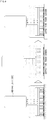
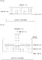
- FIG. 1 is a diagram illustrating a relation between touch units 105 and a touch film 110 included in a touch module 100.
- FIG. 1 is a diagram illustrating a relation between touch units 105, a touch film 110, and a frame unit 115 included in a touch module 100 in which a plurality of touch units 105 including a material which induces capacitance change of a capacitive touch screen is disposed and fabricated in a predesigned unique geometric relation, and those skilled in the art may infer various embodiments for a relation between the touch units 105 and the touch film 110 by referencing and/or modifying FIG. 1 .
- the present invention may include all the inferred embodiments, and the technical feature is not limited to the embodiment shown in FIG. 1 .
- the touch module 100 includes a plurality of touch units 105 each including a material which induces capacitance change of the capacitive touch screen, and disposed in a predesigned unique geometric relation on design, and the touch film 110 including a contact area 110a contacting the capacitive touch screen, and configured to dispose and fix touch units 105 of a specified number corresponding to the geometric relation on design on/to an internal area 110b included on an opposite side of the contact area 110a, or contact the touch units 105 of the specified number corresponding to the geometric relation on design when the touch module 100 touches the capacitive touch screen, and further includes the frame unit 115 including a material which applies capacitance of a human body to the touch units 105.
- the touch units 105 are collective terms for the composition including a capacitance-change inducing material capable of touching the capacitive touch screen in a capacitive mode, and it is preferable that the touch units 105 include a capacitance-change inducing material which is restorable after contraction by an external force (e.g., a pressure).
- an external force e.g., a pressure
- the touch units 105 may be fabricated using at least one conductive material having a rubber-elasticity of a conductive rubber material, a conductive plastic material, and a conductive silicone material, and for example the touch units 105 may be fabricated to have a predesigned hardness (e.g., 80 or lower based on a Shore A hardness tester) and a predesigned electric resistance (e.g., a measured resistance value between a touched portion and a portion electrically connected to a human body of 300 or lower).
- a predesigned hardness e.g. 80 or lower based on a Shore A hardness tester
- a predesigned electric resistance e.g., a measured resistance value between a touched portion and a portion electrically connected to a human body of 300 or lower.
- the touch units 105 may be fabricated using a metallic material, and the metallic material may be any material when it is a metallic material having high electric conductivity (e.g., a measured resistance value between a touched portion and a portion electrically connected to a human body of lower than 1 Ohm) such as gold, silver, copper, aluminum, etc.
- the metallic material is hard to contract and restore, and therefore the metallic material may be provided in the touch module 100 in a form connected with a capacitance-change inducing material which is restorable after contraction.
- the touch units 105 may be fabricated by coating a non-conductive material with a metallic material.
- the non-conductive material include a material which is restorable after contraction.
- the non-conductive material may be provided in the touch module 100 in a form connected with another capacitance-change inducing material which is restorable after contraction.
- the touch units 105 may be fabricated by forming a metal film of a metallic material on the outside surface of a bumper member having an elastic material which is restorable after contraction.
- the bumper member may include a foamed material such as sponge, polyurethane, etc., and the metal film may be fabricated by coating the bumper member with the metallic material and/or by thread spinning or cotton spinning the metallic material.
- the touch units 105 may be formed in a gasket structure for EMI shielding.
- the touch units 105 may be fabricated using a carbon fiber material including a carbon nanotube material or a single walled carbon nanotube material.
- the touch units 105 may be fabricated using a dielectric material including a solid state dielectric material or a liquid state dielectric material and a vessel receiving the dielectric material.
- the dielectric material is a collective term for a material in which a polarization is generated by a voltage or an electric field and a bound charge is generated on a surface, and it is preferable that the dielectric material includes a ferroelectric material (e.g., barium titanate or Rochelle salt, etc.) having a dielectric constant so that a polarization is generated by a voltage or an electric field applied to a surface of a touch screen and a bound charge capable of inducing a capacitance change is generated.
- a ferroelectric material e.g., barium titanate or Rochelle salt, etc.
- the touch units 105 may have a combined form of the first to sixth touch unit embodiments (e.g., a form of a metallic material of the touch unit of the second embodiment combined with a material in which a metal film of a metallic material is formed on outside of a bumper material of an elastic material which is restorable after contraction).
- a combined form of the first to sixth touch unit embodiments e.g., a form of a metallic material of the touch unit of the second embodiment combined with a material in which a metal film of a metallic material is formed on outside of a bumper material of an elastic material which is restorable after contraction.
- the touch unit embodiment of the present invention is not limited to the first to seventh touch unit embodiments, and it is obvious that any material can be included in a scope of a patent when the touch units include a material which induces capacitance change of a capacitive touch screen.
- the touch units 105 fabricated using the first to seventh touch unit embodiments are fabricated including a contact surface having a calculated contact area so that the touch units 105 touch the capacitive touch screen.
- the contact surface of the touch units 105 may be fabricated in a circle shape having a diameter of 3 to 7, or an oval shape or a polygon shape having a contact area corresponding to a circle area of a diameter of 3 to 7.
- the plurality of touch units 105 may be fabricated so that each touch unit has the same height or at least one touch unit is higher than the other touch units 105 by a predetermined reference value or more.
- the touch units 105 touch the capacitive touch screen in a capacitive mode sequentially starting from a highest touch unit 105.
- the plurality of touch units 105 may touch the capacitive touch screen in a capacitive mode with a minute time difference while a pressure is applied to the frame unit 115 and the plurality of touch units 105 slides.
- the touch film 110 is a collective term for the composition which includes a material capable of transferring a capacitance change generated by the touch units 105 to the capacitive touch screen, and preferably the touch film 110 is fabricated in a plane shape including a contact area 110a which contacts the capacitive touch screen.
- the touch film 110 may dispose and fix the touch units 105 on an internal area 110b provided on the opposite side of the contact area 110a included in the touch film 110, or may contact the touch units 105 disposed on and fixed to the frame unit 115.
- the touch film 110 may be disposed on or fixed to the internal area 110b and/or may include a material capable of transferring a capacitance change generated by the touch units 105 to the capacitive touch screen.
- the touch film 110 may include at least one of a non-conductive material and a combination of a conductive material and the non-conductive material in view of an electric conductivity.
- the touch film 110 may include the non-conductive material, and in this case it is preferable that the touch film 110 is fabricated with a thickness equal to or less than 0.2 mm. That is, though the touch film 110 is the non-conductive material when the thickness is equal to or less than 0.2 mm, it is possible to transfer 99% of a capacitance change of a capacitance-change inducing material included in the plurality of touch units 105 to the capacitive touch screen based on electric capacitance of a human body.
- the thickness of the touch film 110 including the non-conductive material may be varied to be proportional to a magnitude of a current or a voltage applied to a surface of the capacitive touch screen, or inversely proportional to resistance of the touch units 105 including a conductive material which transfers human electric capacitance, and it is obvious that the present invention includes even a case of the touch film 110 including the non-conductive material in a scope of a patent.
- the touch film 110 may be fabricated so that a plurality of holes is formed in a lattice structure (or beehive structure) in the non-conductive material, and a metallic material passes through the plurality of holes and is plated on a predetermined area (e.g., about 2 mm) of both surfaces of the touch film 110 and plated holes are formed.
- the metallic material passing through the plating holes and plated on the predetermined area of both surfaces performs a role of transferring a capacitance change of the touch units 105.
- the plating holes are densely disposed (e.g., a distance between areas plated on both surfaces passing through the plating holes is about 2 mm).
- the thickness of the touch film 110 may not be limited by a specific numerical value, but a transfer rate of the capacitance change may be further improved when the thickness is 0.2 mm or less.
- the touch film 110 may be fabricated so that a conductive material (e.g., a metallic material) is embedded inside of a plate of a non-conductive material and a conductive layer is formed.
- the conductive layer may have a shape of a plate or a net.
- the thickness of the touch film 110 itself may not be limited by a specific numerical value, but it is preferable that the touch film 110 is fabricated so that a distance between the conductive layer and the capacitive touch screen is 0.2 mm or less when the touch film 110 contacts the capacitive touch screen.
- the touch film 110 may be fabricated to have a form in which two or more of the first to third conductivity embodiments are combined.
- the embodiment of the touch film 110 of the present invention is not limited to the above-described embodiments, and when the touch film 110 has a material or property capable of transferring a capacitance change generated by the touch units 105 to the capacitive touch screen, it is obvious that the touch film 110 can be included in a scope of a patent described in the claim whatever form or structure it has.
- the touch film 110 may include a material configured to block the plurality of touch units 105 so that the geometric relation formed by the plurality of touch units disposed on or fixed to and/or contacting the internal area 110b is not exposed.
- the touch film 110 in view of a light transmission factor, may include at least one or a combination of two or more of an opaque material, an opaque material disposed on at least one side, a translucent material, a translucent material disposed on at least one side, a transparent material, a transparent material disposed on at least one side, a transmission-factor changing material, and a transmission-factor changing material disposed on at least one side.
- the touch film 110 may include an opaque material capable of transferring a capacitance change generated by a capacitance-change inducing material to the capacitive touch screen.
- the opaque material includes a material having a transmission factor of a light incident on the touch film 110 of 0 %, but even a light transmission factor in which a specified geometric relation of the plurality of touch units 105 is not visually discriminated is defined to be included in the opaque material, and the numerical value may include to the light transmission factor of less than 5 %.
- the touch film 110 may include, on at least one side, an opaque material capable of transferring a capacitance change generated by a capacitance-change inducing material to the capacitive touch screen.
- the touch film 110 may include a transparent material or a translucent material on the other side, and may include a layer or a film of an opaque material or include a form in which an opaque material is coated or painted on the at least one side.
- the touch film 110 may include a translucent material capable of transferring a capacitance change generated by a capacitance-change inducing material to the capacitive touch screen.
- the translucent material refers to a material in which a transmission factor of a light incident on the touch film 110 is not included in a scope of the opaque material and the transparent material.
- the touch film 110 may include, on at least one side, a translucent material capable of transferring a capacitance change generated by a capacitance-change inducing material to the capacitive touch screen.
- the translucent material touch film 110 may include a transparent material or an opaque material on the other side, and may include a layer or a film of a translucent material or include a form in which a translucent material is coated or painted on the at least one side.
- the touch film 110 may include a transparent material capable of transferring a capacitance change generated by a capacitance-change inducing material to the capacitive touch screen.
- the transparent material includes a material having a transmission factor of a light incident on the touch film 110 of 100 %, but even a material having the light transmission factor of 95 % or more may be defined to be included in the transparent material.
- the touch film 110 may include, on at least one side, a transparent material capable of transferring a capacitance change generated by a capacitance-change inducing material to the capacitive touch screen.
- the touch film 110 may include an opaque material or a translucent material on the other side, and may include a layer or a film of a transparent material or include a form in which a transparent material is coated or painted on the at least one side.
- the touch film 110 may include a transmission-factor changing material capable of transferring a capacitance change generated by a capacitance-change inducing material to the capacitive touch screen.
- the transmission-factor changing material is a collective term for a material in which the transmission factor is changed by an electric signal, and for example may include a transmission-factor changing glass material.
- the transmission-factor changing material is not limited to the transmission-factor changing glass material, and when the touch film 110 has a transmission-factor changing material capable of transferring a capacitance change generated by the capacitance-change inducing material to the capacitive touch screen, it is obvious that the touch film 110 can be included in a scope of a patent described in the claim whatever material it includes.
- the touch film 110 may include, on at least one side, a transmission-factor changing material capable of transferring a capacitance change generated by a capacitance-change inducing material to the capacitive touch screen.
- the touch film 110 may include a transparent material, a translucent material, or an opaque material on the other side, and may include a layer or a film of a transmission-factor changing material or include a form in which a transmission-factor changing material is coated or painted on the at least one side.
- the touch film 110 may be fabricated to have a form in which two or more of the first to eighth transmission factor embodiments are combined.
- the embodiment of the touch film 110 of the present invention is not limited to the above-described embodiments, and when the touch film 110 has a material or property capable of transferring a capacitance change generated by the touch units 105 to the capacitive touch screen, it is obvious that the touch film 110 can be included in a scope of a patent described in the claim whatever light transmission factor it has.
- a capacitive touch is generated on the capacitive touch screen by the touch units 105 disposed on and fixed to the internal area 110b of the touch film 110 and/or contacting the internal area 110b of the touch film 110.
- the plurality of touch units 105 may be disposed on and fixed to the frame unit 115 and, in this case, the frame unit 115 disposes and fixes the plurality of touch units 105 in a predesigned unique geometric relation on design.
- the touch module 100 in which the plurality of touch units 105 is disposed on and fixed to the frame unit 115 touches the capacitive touch screen
- a plurality of touch points touches the capacitive touch screen and is recognized according to a geometric relation on design of the touch units 105 disposed on and fixed to the frame unit 115. That is, in the first touch unit disposition embodiment, the frame unit 115 disposes and fixes the plurality of touch units 105 in a geometric relation on design projected on the capacitive touch screen.
- the plurality of touch units 105 may be disposed on and fixed to the internal area 110b of the touch film 110 and, in this case, the internal area 110b of the touch film 110 disposes and fixes the plurality of touch units 105 in a predesigned unique geometric relation on design.
- the touch module 100 in which the plurality of touch units 105 is disposed on and fixed to the internal area 110b of the touch film 110 touches the capacitive touch screen
- a plurality of touch points touches the capacitive touch screen and is recognized according to a geometric relation on design of the touch units 105 disposed on and fixed to the internal area 110b of the touch film 110. That is, in the second touch unit disposition embodiment, the internal area 110b of the touch film 110 disposes and fixes the plurality of touch units 105 in a geometric relation on design projected on the capacitive touch screen.
- a part of the plurality of touch units 105 may be disposed on and fixed to the internal area 110b of the touch film 110 and the rest touch units 105 may be disposed on and fixed to the frame unit 115.
- the geometric relation on design disposing the plurality of touch units 105 is defined as a geometric relation in which a disposed position of a part of the plurality of touch units 105 disposed on and fixed to the internal area 110b of the touch film 110 and a disposed position of the rest touch units 105 disposed on and fixed to the frame unit 115 are combined.
- the geometric relation on design includes a geometric relation of the touch units 105 in which a disposed position of a part of the plurality of touch units 105 disposed on and fixed to the internal area 110b of the touch film 110 and a disposed position of the rest touch units 105 disposed on and fixed to the frame unit 115 are combined and projected on the capacitive touch screen.
- the geometric relation on design which disposes the plurality of touch units 105 may include at least one relation of a distance relation on design between centers of respective touch units 105, an angle relation on design between centers of respective touch units, and a combination of the distance relation on design and the angle relation on design between centers of respective touch units 105.
- the geometric relation on design which disposes the plurality of touch units 105 may include a geometric relation in which one specified touch unit 105 of the plurality of touch units 105 is disposed on and fixed to a fixed position predetermined on design.
- the geometric relation on design may include at least one relation of a distance relation on design and an angle relation on design between a center of the specified touch unit 105 and centers of the other touch units 105, and a combination of the distance relation on design and the angle relation on design between a center of the specified touch unit 105 and centers of the other touch units 105.
- the specified touch unit 105 disposed on and fixed to a fixed position predetermined on design may be an indicator which sets a reference point of the geometric relation on design.
- the geometric relation on design may include at least one relation of a distance relation on design and an angle relation on design between a reference point determined by the specified touch unit 105 and a center of each touch unit 105, and a combination of the distance relation on design and the angle relation on design between the reference point determined by the specified touch unit 105 and the center of each touch unit 105.
- the specified touch unit 105 or the reference point provides a reference for reading out the geometric relation of touch points whatever position or in whatever direction of the capacitive touch screen the touch module 100 touches.
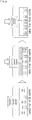
- FIGS. 2 to 5 are diagrams illustrating a relation among touch units 105, a touch film 110, and a frame unit 115 included in a touch module 100 in accordance with a first embodiment of the present invention.
- FIGS. 2 to 5 illustrate embodiments in which the plurality of touch units 105 each having the same height are disposed on and fixed to the internal area 110b of the touch film 110 in a predesigned unique geometric relation on design.
- the touch module 100 of FIG. 2 includes the touch film 110 including the internal area 110b which disposes and fixes the plurality of touch units 105 each having the same height in a predesigned unique geometric relation on design, and includes the frame unit 115 which is separated from the touch units 105 disposed on and fixed to the internal area 110b of the touch film 110 by a specified distance or more after the contact area 110a of the touch film 110 contacts the capacitive touch screen and before a pressure is applied.
- the touch module 100 includes a housing unit 120 which fixes the touch film 110 and protects the touch units 105 disposed on and fixed to the internal area 110b of the touch film 110.
- the touch film 110 is fixed to the housing unit 120, and the touch units 105 disposed on and fixed to the internal area 110b of the touch film 110 are not visually exposed outside by the touch film 110 and the housing unit 120.
- the frame unit 115 having a facing surface capable of contacting the touch units 105 disposed on and fixed to the internal area 110b of the touch film 110 is provided inside of the housing unit 120.
- One side of the frame unit 115 protrudes outside and receives electric capacitance of a human body which grasps the touch module 100 with a hand.
- the frame unit 115 protruding outside of the housing unit 120 may be connected to a holder unit 130 which may be grasped by a hand of a human body, and the holder unit 130 may include a conductive material electrically connected to the frame unit 115.
- the touch module 100 includes a spring 125 which separates the touch units 105 disposed on and fixed to the internal area 110b of the touch film 110 from the frame unit 115 by a specified distance or more after the contact area 110a of the touch film 110 contacts the capacitive touch screen and before a pressure is applied. Meanwhile, the spring 125 may be omitted as an embodiment of FIG. 5 .
- the frame unit 115 contacts the touch units 105 disposed on and fixed to the internal area 110b of the touch film 110, at this time capacitance of the human body which applies the pressure is applied to the touch units 105 disposed on and fixed to the internal area 110b of the touch film 110 through the frame unit 115, and the plurality of touch units 105 disposed on and fixed to the internal area 110b of the touch film 110 touch the capacitive touch screen and are recognized in a predesigned unique geometric relation on design.
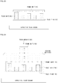
- FIGS. 6 to 9 are diagrams illustrating a relation among touch units 105, a touch film 110, and a frame unit 115 included in a touch module 100 in accordance with a second embodiment of the present invention.
- FIGS. 6 to 9 illustrate embodiments in which the plurality of touch units 105 each having the same height are disposed on and fixed to the frame unit 115 in a predesigned unique geometric relation on design.
- the touch module 100 of FIG. 6 includes the frame unit 115 which disposes and fixes the plurality of touch units 105 each having the same height in a predesigned unique geometric relation on design, and includes the touch film 110 which is separated from the touch units 105 disposed on and fixed to the frame unit 115 by a specified distance or more after the contact area 110a of the touch film 110 contacts the capacitive touch screen and before a pressure is applied.
- the touch module 100 includes a housing unit 120 which fixes the touch film 110 and protects the touch units 105 disposed on and fixed to the frame unit 115.
- the touch film 110 is fixed to the housing unit 120, and the touch units 105 disposed on and fixed to the frame unit 115 are not visually exposed outside by the touch film 110 and the housing unit 120.
- One side of the frame unit 115 protrudes outside of the housing unit 120 and receives electric capacitance of a human body which grasps the touch module 100 with a hand. Meanwhile, the frame unit 115 protruding outside of the housing unit 120 may be connected to a holder unit 130 which may be grasped by a hand of a human body, and the holder unit 130 may include a conductive material electrically connected to the frame unit 115.
- the touch module 100 includes a spring 125 which separates the touch units 105 disposed on and fixed to the frame unit 115 from the internal area 110b of the touch film 110 by a specified distance or more after the contact area 110a of the touch film 110 contacts the capacitive touch screen and before a pressure is applied. Meanwhile, the spring 125 may be omitted as an embodiment of FIG. 9 .
- the touch units 105 disposed on and fixed to the frame unit 115 contact the internal area 110b of the touch film 110, at this time capacitance of the human body which applies the pressure is applied to the touch units 105 through the frame unit 115, and the plurality of touch units 105 disposed on and fixed to the frame unit 115 contacts the internal area 110b of the touch film 110 and touch the capacitive touch screen and are recognized in a predesigned unique geometric relation on design.
- FIGS. 10 to 13 are diagrams illustrating a relation among touch units 105, a touch film 110, and a frame unit 115 included in a touch module 100 in accordance with a third embodiment of the present invention.
- FIGS. 10 to 13 illustrate embodiments in which a part of the plurality of touch units 105 each having the same height is disposed on and fixed to the internal area 110b of the touch film 110, and the rest touch units of the plurality of touch units 105 are disposed on and fixed to the frame unit 115.
- the touch module 100 of FIG. 10 includes the touch film 110 including the internal area 110b which disposes and fixes a part of the plurality of touch units 105 each having the same height, and the frame unit 115 which disposes and fixes the rest touch units 105 except the touch units 105 disposed on and fixed to the internal area 110b of the touch film 110, and a geometric relation in which a disposed position of the touch units 105 disposed on and fixed to the internal area 110b of the touch film 110 and a disposed position of the touch units 105 disposed on and fixed to the frame unit 115 are combined forms a predesigned unique geometric relation on design.
- the touch units 105 disposed on and fixed to the internal area 110b of the touch film 110 are separated from the frame unit 115 by a specified distance or more, and the touch units 105 disposed on and fixed to the frame unit 115 are separated from the internal area 110b of the touch film 110, after the contact area 110a of the touch film 110 contacts the capacitive touch screen and before a pressure is applied.
- the touch module 100 includes a housing unit 120 which fixes the touch film 110 and protects the touch units 105 dispersed and disposed on and fixed to the internal area 110b of the touch film 110 and the frame unit 115.
- the touch film 110 is fixed to the housing unit 120, and the touch units 105 dispersed and disposed on and fixed to the internal area 110b of the touch film 110 and the frame unit 115 are not visually exposed outside by the touch film 110 and the housing unit 120.
- One side of the frame unit 115 protrude outside of the housing unit 120 and receives electric capacitance of a human body which grasps the touch module 100 with a hand. Meanwhile, the frame unit 115 protruding outside of the housing unit 120 may be connected to a holder unit 130 which may be grasped by a hand of a human body, and the holder unit 130 may include a conductive material electrically connected to the frame unit 115.
- the touch module 100 includes a spring 125 which separates the touch units 105 disposed on and fixed to the frame unit 115 from the internal area 110b of the touch film 110 by a specified distance or more after the contact area 110a of the touch film 110 contacts the capacitive touch screen and before a pressure is applied. Meanwhile, the spring 125 may be omitted as an embodiment of FIG. 13 .
- the touch units 105 disposed on and fixed to the internal area 110b of the touch film 110 contact the frame unit 115, and the touch units 105 disposed on and fixed to the frame unit 115 contact the internal area 110b of the touch film 110.
- capacitance of the human body which applies the pressure is applied to the touch units 105 through the frame unit 115, and the touch units 105 disposed on and fixed to the internal area 110b of the touch film 110 and the frame unit 115 touch the capacitive touch screen and are recognized in a predesigned unique geometric relation on design.
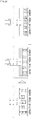
- FIGS. 14 to 16 are diagrams illustrating a relation among touch units 105, a touch film 110, and a frame unit 115 included in a touch module 100 in accordance with a fourth embodiment of the present invention.
- FIGS. 14 to 16 illustrate embodiments in which the plurality of touch units 105 including at least one touch unit 105 having a height different from those of the other touch units 105 is disposed on and fixed to the internal area 110b of the touch film 110 in a predesigned unique geometric relation on design.
- the touch module 100 of FIG. 14 includes the touch film 110 including the internal area 110b which disposes and fixes the plurality of touch units 105 including at least one touch unit 105 having a height different from those of the other touch units 105 in a predesigned unique geometric relation on design, and includes the frame unit 115 which is separated from the touch units 105 disposed on and fixed to the internal area 110b of the touch film 110 by a specified distance or more after the contact area 110a of the touch film 110 contacts the capacitive touch screen and before a pressure is applied.
- the touch module 100 includes a housing unit 120 which fixes the touch film 110 and protects the touch units 105 disposed on and fixed to the internal area 110b of the touch film 110.
- the touch film 110 is fixed to the housing unit 120, and the touch units 105 disposed on and fixed to the internal area 110b of the touch film 110 are not visually exposed outside by the touch film 110 and the housing unit 120.
- the frame unit 115 having a facing surface capable of contacting the touch units 105 disposed on and fixed to the internal area 110b of the touch film 110 is provided inside of the housing unit 120.
- One side of the frame unit 115 protrudes outside of the housing unit 120 and receives electric capacitance of a human body which grasps the touch module 100 with a hand.
- the frame unit 115 protruding outside of the housing unit 120 may be connected to a holder unit 130 which may be grasped by a hand of a human body, and the holder unit 130 may include a conductive material electrically connected to the frame unit 115.
- the touch module 100 includes a spring 125 which separates the touch units 105 disposed on and fixed to the internal area 110b of the touch film 110 from the frame unit 115 by a specified distance or more after the contact area 110a of the touch film 110 contacts the capacitive touch screen and before a pressure is applied.
- the touch units 105 disposed on and fixed to the internal area 110b of the touch film 110 contact the frame unit 115 sequentially starting from a highest touch unit 105, at this time capacitance of the human body which applies the pressure is sequentially applied to the touch units 105 disposed on and fixed to the internal area 110b of the touch film 110 with different heights through the frame unit 115, and the plurality of touch units 105 disposed on and fixed to the internal area 110b of the touch film 110 touch the capacitive touch screen and are recognized in a predesigned unique geometric relation on design.
- FIGS. 17 to 19 are diagrams illustrating a relation among touch units 105, a touch film 110, and a frame unit 115 included in a touch module 100 in accordance with a fifth embodiment of the present invention.
- FIGS. 17 to 19 illustrate embodiments in which the plurality of touch units 105 including at least one touch unit 105 having a height different from those of the other touch units 105 are disposed on and fixed to the frame unit 115 in a predesigned unique geometric relation on design.
- the touch module 100 of FIG. 17 includes the frame unit 115 which dispose and fix the plurality of touch units 105 including at least one touch unit 105 having a height different from those of the other touch units 105 in a predesigned unique geometric relation on design, and includes the touch film 110 which is separated from the touch units 105 disposed on and fixed to the frame unit 115 by a specified distance or more after the contact area 110a of the touch film 110 contacts the capacitive touch screen and before a pressure is applied.
- the touch module 100 includes a housing unit 120 which fixes the touch film 110 and protects the touch units 105 disposed on and fixed to the frame unit 115.
- the touch film 110 is fixed to the housing unit 120, and the touch units 105 disposed on and fixed to the frame unit 115 are not visually exposed outside by the touch film 110 and the housing unit 120.
- One side of the frame unit 115 protrudes outside of the housing unit 120 and receives electric capacitance of a human body which grasps the touch module 100 with a hand. Meanwhile, the frame unit 115 protruding outside of the housing unit 120 may be connected to a holder unit 130 which may be grasped by a hand of a human body, and the holder unit 130 may include a conductive material electrically connected to the frame unit 115.
- the touch module 100 includes a spring 125 which separates the touch units 105 disposed on and fixed to the frame unit 115 from the internal area 110b of the touch film 110 by a specified distance or more after the contact area 110a of the touch film 110 contacts the capacitive touch screen and before a pressure is applied.
- the touch units 105 disposed on and fixed to the frame unit 115 contact the internal area 110b of the touch film 110 sequentially starting from a highest touch unit 105, at this time capacitance of the human body which applies the pressure is applied to the touch units 105, and the plurality of touch units 105 disposed on and fixed to the frame unit 115 sequentially contact the internal area 110b of the touch film 110 and sequentially touch the capacitive touch screen and are recognized in a predesigned unique geometric relation on design.
- FIGS. 20 to 22 are diagrams illustrating a relation among touch units 105, a touch film 110, and a frame unit 115 included in a touch module 100 in accordance with a sixth embodiment of the present invention.
- FIGS. 20 to 22 illustrate embodiments in which a part of the plurality of touch units 105 including at least one touch unit 105 having a height different from those of the other touch units 105 is disposed on and fixed to the internal area 110b of the touch film 110, and the rest touch units of the plurality of touch units 105 are disposed on and fixed to the frame unit 115.
- the touch module 100 of FIG. 20 includes the touch film 110 including the internal area 110b which disposes and fixes a part of the plurality of touch units 105 including at least one touch unit 105 having a height different from those of the other touch units 105, and the frame unit 115 which disposes and fixes the rest touch units 105 except the touch units 105 disposed on and fixed to the internal area 110b of the touch film 110, and a geometric relation in which a disposed position of the touch units 105 disposed on and fixed to the internal area 110b of the touch film 110 and a disposed position of the touch units 105 disposed on and fixed to the frame unit 115 are combined forms a predesigned unique geometric relation on design.
- the touch units 105 disposed on and fixed to the internal area 110b of the touch film 110 are separated from the frame unit 115 by a specified distance or more, and the touch units 105 disposed on and fixed to the frame unit 115 are separated from the internal area 110b of the touch film 110, after the contact area 110a of the touch film 110 contacts the capacitive touch screen and before a pressure is applied.
- the touch module 100 includes a housing unit 120 which fixes the touch film 110 and protects the touch units 105 dispersed and disposed on and fixed to the internal area 110b of the touch film 110 and the frame unit 115.
- the touch film 110 is fixed to the housing unit 120, and the touch units 105 dispersed and disposed on and fixed to the internal area 110b of the touch film 110 and the frame unit 115 are not visually exposed outside by the touch film 110 and the housing unit 120.
- One side of the frame unit 115 protrudes outside of the housing unit 120 and receives electric capacitance of a human body which grasps the touch module 100 with a hand. Meanwhile, the frame unit 115 protruding outside of the housing unit 120 may be connected to a holder unit 130 which may be grasped by a hand of a human body, and the holder unit 130 may include a conductive material electrically connected to the frame unit 115.
- the touch module 100 includes a spring 125 which separates the touch units 105 disposed on and fixed to the frame unit 115 from the internal area 110b of the touch film 110 by a specified distance or more after the contact area 110a of the touch film 110 contacts the capacitive touch screen and before a pressure is applied.
- the touch units 105 disposed on and fixed to the internal area 110b of the touch film 110 contact the frame unit 115 sequentially starting from a highest touch unit 105, and the touch units 105 disposed on and fixed to the frame unit 115 contact the internal area 110b of the touch film 110 sequentially starting from a highest touch unit 105.
- the highest touch unit 105 of the plurality of touch units 105 is disposed on and fixed to the internal area 110b of the touch film 110, the plurality of touch units 105 contact the frame unit 115 starting from a highest touch unit 105 by the pressure.
- the plurality of touch units 105 contact the internal area 110b of the touch film 110 starting from a highest touch unit 105 by the pressure.
- capacitance of the human body which applies the pressure is first applied to the touch units 105 disposed on and fixed to the frame unit 115, and then applies to the touch units disposed on and fixed to the internal area 110b of the touch film 110 as the touch units 105 disposed on and fixed to the internal area 110b of the touch film 110 contact the frame unit 115.
- the touch units 105 disposed on and fixed to the internal area 110b of the touch film 110 contact the frame unit 115 and an order in which the touch units 105 disposed on and fixed to the frame unit 115 contact the internal area 110b of the touch film 110, the touch units 105 dispersed and disposed on and fixed to the internal area 110b of the touch film 110 and the frame unit 115 with different heights sequentially touch the capacitive touch screen and are recognized in a predesigned unique geometric relation on design.
- FIGS. 23 to 25 are diagrams illustrating a relation among touch units 105, a touch film 110, and a frame unit 115 included in a touch module 100 in accordance with a seventh embodiment of the present invention.
- FIGS. 23 to 25 illustrate embodiments in which the plurality of touch units 105 including at least one touch unit 105 having a height different from those of the other touch units 105 are disposed on and fixed to the internal area 110b of the touch film 110 in a predesigned unique geometric relation on design.
- the touch module 100 of FIG. 23 includes the touch film 110 including the internal area 110b which disposes and fixes the plurality of touch units 105 including at least one touch unit 105 having a height different from those of the other touch units 105 in a predesigned unique geometric relation on design, and includes the frame unit 115 which maintains a contacted state with a highest touch unit 105 among the touch units 105 disposed on and fixed to the internal area 110b of the touch film 110.
- the touch module 100 includes a housing unit 120 which fixes the touch film 110 and protects the touch units 105 disposed on and fixed to the internal area 110b of the touch film 110.
- the touch film 110 is fixed to the housing unit 120, and the touch units 105 disposed on and fixed to the internal area 110b of the touch film 110 are not visually exposed outside by the touch film 110 and the housing unit 120.
- the frame unit 115 having a facing surface capable of contacting the touch units 105 disposed on and fixed to the internal area 110b of the touch film 110 is provided inside of the housing unit 120.
- One side of the frame unit 115 protrudes outside of the housing unit 120 and receives electric capacitance of a human body which grasps the touch module 100 with a hand.
- the frame unit 115 protruding outside of the housing unit 120 may be connected to a holder unit 130 which may be grasped by a hand of a human body, and the holder unit 130 may include a conductive material electrically connected to the frame unit 115.
- the touch units 105 disposed on and fixed to the internal area 110b of the touch film 110 contact the frame unit 115 sequentially based on respective heights, at this time capacitance of the human body which applies the pressure is sequentially applied to respective touch units 105 disposed on and fixed to the internal area 110b of the touch film 110 with different heights through the frame unit 115, and the plurality of touch units 105 disposed on and fixed to the internal area 110b of the touch film 110 touch the capacitive touch screen and are recognized in a predesigned unique geometric relation on design.
- FIGS. 26 to 28 are diagrams illustrating a relation among touch units 105, a touch film 110, and a frame unit 115 included in a touch module 100 in accordance with a eighth embodiment of the present invention.
- FIGS. 26 to 28 illustrate embodiments in which the plurality of touch units 105 including at least one touch unit 105 having a height different from those of the other touch units 105 are disposed on and fixed to the frame unit 115 in a predesigned unique geometric relation on design.
- the touch module 100 of FIG. 26 includes the frame unit 115 which disposes and fixes the plurality of touch units 105 including at least one touch unit 105 having a height different from those of the other touch units 105 in a predesigned unique geometric relation on design, and includes the touch film 110 which maintains a contacted state with a highest touch unit 105 among the touch units 105 disposed on and fixed to the frame unit 115.
- the touch module 100 includes a housing unit 120 which fixes the touch film 110 and protects the touch units 105 disposed on and fixed to the frame unit 115.
- the touch film 110 is fixed to the housing unit 120, and the touch units 105 disposed on and fixed to the frame unit 115 are not visually exposed outside by the touch film 110 and the housing unit 120.
- One side of the frame unit 115 protrudes outside of the housing unit 120 and receives electric capacitance of a human body which grasps the touch module 100 with a hand. Meanwhile, the frame unit 115 protruding outside of the housing unit 120 may be connected to a holder unit 130 which may be grasped by a hand of a human body, and the holder unit 130 may include a conductive material electrically connected to the frame unit 115.
- the touch units 105 disposed on and fixed to the frame unit 115 contact the internal area 110b of the touch film 110 sequentially based on respective heights, at this time capacitance of the human body which applies the pressure is sequentially applied to respective touch units 105 through the frame unit 115, and the plurality of touch units 105 disposed on and fixed to the frame unit 115 sequentially contacts the internal area 110b of the touch film 110 and touch the capacitive touch screen and are recognized in a predesigned unique geometric relation on design.
- FIGS. 29 to 31 are diagrams illustrating a relation among touch units 105, a touch film 110, and a frame unit 115 included in a touch module 100 in accordance with a ninth embodiment of the present invention.
- FIGS. 29 to 31 illustrate embodiments in which a part of the plurality of touch units 105 including at least one touch unit of the housing unit 120 the other touch units 105 is disposed on and fixed to the internal area 110b of the touch film 110, and the rest touch units of the plurality of touch units 105 are disposed on and fixed to the frame unit 115.
- the touch module 100 of FIG. 29 includes the touch film 110 including the internal area 110b which dispose and fix a part of the plurality of touch units 105 including at least one touch unit of the housing unit 120 the other touch units 105, and the frame unit 115 which disposes and fixes the rest touch units 105 except the touch units 105 disposed on and fixed to the internal area 110b of the touch film 110, and a geometric relation in which a disposed position of the touch units 105 disposed on and fixed to the internal area 110b of the touch film 110 and a disposed position of the touch units 105 disposed on and fixed to the frame unit 115 are combined forms a predesigned unique geometric relation on design.
- the frame unit 115 disposes and fixes a highest touch unit 105 among the plurality of touch units 105, and the highest touch unit 105 disposed on and fixed to the frame unit 115 maintains a contacted state with the internal area 110b of the touch film 110.
- the touch module 100 includes a housing unit 120 which fixes the touch film 110 and protects the touch units 105 dispersed and disposed on and fixed to the internal area 110b of the touch film 110 and the frame unit 115.
- the touch film 110 is fixed to the housing unit 120, and the touch units 105 dispersed and disposed on and fixed to the internal area 110b of the touch film 110 and the frame unit 115 are not visually exposed outside by the touch film 110 and the housing unit 120.
- One side of the frame unit 115 protrudes outside of the housing unit 120 and receives electric capacitance of a human body which grasps the touch module 100 with a hand. Meanwhile, the frame unit 115 protruding outside of the housing unit 120 may be connected to a holder unit 130 which may be grasped by a hand of a human body, and the holder unit 130 may include a conductive material electrically connected to the frame unit 115.
- the touch units 105 disposed on and fixed to the internal area 110b of the touch film 110 contact the frame unit 115 sequentially starting from the highest touch unit 105, and the touch units 105 disposed on and fixed to the frame unit 115 contact the internal area 110b of the touch film 110 sequentially starting from the highest touch unit 105.
- capacitance of the human body which applies the pressure is first applied to the highest touch unit 105 of the touch units 105 disposed on and fixed to the frame unit 115 and the internal area 110b of the touch film 110, and also applied to the touch units 105 disposed on and fixed to the internal area 110b of the touch film 110 as the touch units 105 disposed on and fixed to the internal area 110b of the touch film 110 contact the frame unit 115.
- the highest touch unit 105 disposed on and fixed to the frame unit 115 of the touch units 105 dispersed and disposed on and fixed to the internal area 110b of the touch film 110 and the frame unit 115 with different heights is first touched and recognized, and the rest touch units 105 are sequentially touched on the capacitive touch screen and recognized according to a predesigned unique geometric relation on design based on an order in which the touch units 105 disposed on and fixed to the internal area 110b of the touch film 110 contact the frame unit 115 and an order in which the touch units 105 disposed on and fixed to the frame unit 115 contact the internal area 110b of the touch film 110 by the pressure.
- FIGS. 32 to 34 are diagrams illustrating a relation among touch units 105, a touch film 110, and a frame unit 115 included in a touch module 100 in accordance with a tenth embodiment of the present invention.
- FIGS. 32 to 34 illustrate embodiments in which a part of the plurality of touch units 105 including at least one touch unit 105 having a height different from those of the other touch units 105 is disposed on and fixed to the internal area 110b of the touch film 110, and the rest touch units of the plurality of touch units 105 are disposed on and fixed to the frame unit 115.
- the touch module 100 of FIG. 32 includes the touch film 110 including the internal area 110b which disposes and fixes a part of the plurality of touch units 105 including at least one touch unit 105 having a height different from those of the other touch units 105, and the frame unit 115 which disposes and fixes the rest touch units 105 except the touch units 105 disposed on and fixed to the internal area 110b of the touch film 110, and a geometric relation in which a disposed position of the touch units 105 disposed on and fixed to the internal area 110b of the touch film 110 and a disposed position of the touch units 105 disposed on and fixed to the frame unit 115 are combined forms a predesigned unique geometric relation on design.
- the internal area 110b of the touch film 110 disposes and fixes a highest touch unit 105 among the plurality of touch units 105, and the highest touch unit 105 disposed on and fixed to the internal area 110b of the touch film 110 maintains a contacted state with the frame unit 115.
- the touch module 100 includes a housing unit 120 which fixes the touch film 110 and protects the touch units 105 dispersed and disposed on and fixed to the internal area 110b of the touch film 110 and the frame unit 115.
- the touch film 110 is fixed to the housing unit 120, and the touch units 105 dispersed and disposed on and fixed to the internal area 110b of the touch film 110 and the frame unit 115 are not visually exposed outside by the touch film 110 and the housing unit 120.
- One side of the frame unit 115 protrudes outside of the housing unit 120 and receives electric capacitance of a human body which grasps the touch module 100 with a hand. Meanwhile, the frame unit 115 protruding outside of the housing unit 120 may be connected to a holder unit 130 which may be grasped by a hand of a human body, and the holder unit 130 may include a conductive material electrically connected to the frame unit 115.
- the touch units 105 disposed on and fixed to the internal area 110b of the touch film 110 contact the frame unit 115 sequentially starting from the highest touch unit 105, and the touch units 105 disposed on and fixed to the frame unit 115 contact the internal area 110b of the touch film 110 sequentially starting from the highest touch unit 105.
- capacitance of the human body which applies the pressure is first applied to the touch units 105 disposed on and fixed to the frame unit 115, and also applied to the touch units 105 disposed on and fixed to the internal area 110b of the touch film 110 as the touch units 105 disposed on and fixed to the internal area 110b of the touch film 110 contact the frame unit 115.
- the highest touch unit 105 disposed on and fixed to the internal area 110b of the touch film 110 dispersed and disposed on and fixed to the internal area 110b of the touch film 110 and the frame unit 115 with different heights is first touched and recognized, and the rest touch units 105 are sequentially touched on the capacitive touch screen and recognized according to a predesigned unique geometric relation on design based on an order in which the touch units 105 disposed on and fixed to the internal area 110b of the touch film 110 contact the frame unit 115 and an order in which the touch units 105 disposed on and fixed to the frame unit 115 contact the internal area 110b of the touch film 110 by the pressure.
- FIGS. 35 to 39 are diagrams illustrating a process of fabricating a touch module 100 in accordance with an embodiment of the present invention.
- FIGS. 35 to 39 illustrate a process of fabricating a touch module 100 in which touch units 105 having different heights are disposed on and fixed to the internal area 110b of the touch film 110 in a predesigned unique geometric relation on design and a specified distance or more between the touch units 105 and the frame unit 115 is maintained through the spring 125.
- Those skilled in the art may infer various embodiments (e.g., embodiments in which a part of steps or processes is omitted or the order is changed) for a fabrication process of the touch module 100 by referring to and/or modifying FIGS. 35 to 39 , and the present invention includes all the embodiments which can be inferred, and the technical feature is not limited to embodiments illustrated in FIGS.
- the plurality of touch units 105 in which at least one touch unit 105 having a height different from those of the other touch units 105, and the embedded plate unit135 for embedding the plurality of touch units 105 are provided.
- a unique geometric relation to dispose the plurality of touch units 105 is designed, and embedded holes 140 are formed in the embedded plate unit135 based on the designed unique geometric relation.
- the geometric relation on design may include at least one relation of a distance relation on design and an angle relation on design between centers of respective embedded holes 140, and combination of the distance relation on design and the angle relation on design between centers of respective embedded holes 140.
- the geometric relation on design to dispose the plurality of embedded holes 140 may include a geometric relation in which one specified embedded hole 140 of the plurality of embedded holes 140 is disposed on and fixed to a fixed position predetermined on design.
- the geometric relation on design may include at least one relation of a distance relation on design and an angle relation on design between a center of the specified embedded hole 140 and centers of the rest embedded holes 140, and combination of the distance relation on design and the angle relation on design between the center of the specified embedded hole 140 and the centers of the rest embedded holes 140.
- the specified embedded hole 140 disposed on and fixed to a fixed position predetermined on design may be an indicator for determining a reference point of the geometric relation on design.
- the geometric relation on design may include at least one relation of a distance relation on design and an angle relation on design between a reference point determined by the specified embedded hole 140 and centers of respective embedded holes 140, and combination of the distance relation on design and the angle relation on design between the reference point determined by the specified embedded hole 140 and the centers of respective embedded holes 140.
- the embedded plate unit135 in which the embedded holes 140 are formed in the predesigned unique geometric relation on design is stacked on the internal area 110b of the touch film 110, and the plurality of touch units 105 are embedded in the embedded holes 140 of the embedded plate unit135 and fixed to the internal area 110b of the touch film 110.
- the plurality of touch units 105 embedded in the embedded holes 140 of the embedded plate unit 135 form a geometric relation on design the same as a geometric relation on design of the embedded holes 140. Meanwhile, when the plurality of touch units 105 are fixed to the internal area 110b of the touch film 110, the embedded plate may be removed.
- the housing unit 120 to fix the touch film 110 is provided, an external frame unit 115 which is outside of the housing unit 120 and an internal frame unit 115 which is inside of the housing unit 120 are provided, the spring 125 included between the external frame unit 115 and the internal frame unit 115 is provided, and then a column of the internal frame unit 115 is inserted in an inserting hole of the housing unit 120 and combined with the external frame unit 115, and the spring 125 is positioned between the internal frame unit 115 and the external frame unit 115, and the internal frame unit 115 contacts the housing unit 120.
- the internal frame unit 115 and the external frame unit 115 may be coupled by a bolt coupling.
- the touch module 100 may be fabricated as shown in FIG. 39 by fixing the touch film 110 fabricated as FIG. 36 to the housing unit 120 fabricated through the process of FIG. 37 .
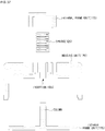
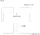
- FIGS. 40 to 44 are diagrams illustrating a process of fabricating a touch module in accordance with another embodiment of the present invention.
- FIGS. 40 to 44 illustrate a process of fabricating a touch module 100 in which touch units 105 having different heights are disposed on and fixed to the internal area 110b of the touch film 110 in a predesigned unique geometric relation on design.
- Those skilled in the art may infer various embodiments (e.g., embodiments in which a part of steps or processes is omitted or the order is changed) for a fabrication process of the touch module 100 by referring to and/or modifying FIGS. 40 to 44 , and the present invention includes all the embodiments which can be inferred, and the technical feature is not limited to embodiments illustrated in FIGS. 40 to 44 .
- the plurality of touch units 105 in which at least one touch unit 105 has a height different from those of the other touch units 105, and embedded plate unit135 for embedding the plurality of touch units 105 are provided.
- a unique geometric relation for disposing the plurality of touch units 105 is designed, and embedded holes 140 are formed in the embedded plate unit135 according to the designed unique geometric relation, and then as shown in FIG. 41 , the embedded plate unit 135 is stacked on the touch film 110 and at the same time the plurality of touch units 105 are embedded in the embedded holes 140 of the holder unit 135 and fixed to the internal area 110b of the touch film 110.
- the plurality of touch units 105 fixed to the internal area 110b of the touch film 110 form a geometric relation on design the same as a geometric relation on design of the embedded holes 140.
- the housing unit 120 to fix the touch film 110 is provided, and the frame unit 115 included in the housing unit 120 is provided, and a column of the internal frame unit 115 is inserted in an inserting hole of the housing unit 120 as shown in FIG. 43 , and then the touch module 100 may be fabricated as shown in FIG. 44 by fixing the touch film 110 fabricated as FIG. 41 to the housing unit 120.
Landscapes
- Engineering & Computer Science (AREA)
- Theoretical Computer Science (AREA)
- General Engineering & Computer Science (AREA)
- Physics & Mathematics (AREA)
- General Physics & Mathematics (AREA)
- Human Computer Interaction (AREA)
- Computer Security & Cryptography (AREA)
- Computer Hardware Design (AREA)
- Software Systems (AREA)
- Position Input By Displaying (AREA)
- Switches That Are Operated By Magnetic Or Electric Fields (AREA)
- User Interface Of Digital Computer (AREA)
Priority Applications (1)
| Application Number | Priority Date | Filing Date | Title |
|---|---|---|---|
| PL15803661T PL3151101T3 (pl) | 2014-06-02 | 2015-06-01 | Moduł dotykowy wielokrotnego dotyku |
Applications Claiming Priority (7)
| Application Number | Priority Date | Filing Date | Title |
|---|---|---|---|
| KR1020140066718A KR101481475B1 (ko) | 2014-06-02 | 2014-06-02 | 다중 순차 터치용 터치모듈 |
| KR20140066717A KR101482660B1 (ko) | 2014-06-02 | 2014-06-02 | 터치막을 구비한 다중 터치용 터치모듈 |
| KR1020140068395A KR101481477B1 (ko) | 2014-06-05 | 2014-06-05 | 다중 순차 터치용 터치모듈 |
| KR1020140069164A KR102238931B1 (ko) | 2014-06-09 | 2014-06-09 | 터치모듈과 그 제조 방법 |
| KR1020140069168A KR101507058B1 (ko) | 2014-06-09 | 2014-06-09 | 터치모듈과 그 제조 방법 |
| KR1020140069173A KR101482667B1 (ko) | 2014-06-09 | 2014-06-09 | 터치모듈과 그 제조 방법 |
| PCT/KR2015/005470 WO2015186939A1 (fr) | 2014-06-02 | 2015-06-01 | Module tactile pour touchers multiples |
Publications (3)
| Publication Number | Publication Date |
|---|---|
| EP3151101A1 true EP3151101A1 (fr) | 2017-04-05 |
| EP3151101A4 EP3151101A4 (fr) | 2017-12-13 |
| EP3151101B1 EP3151101B1 (fr) | 2020-10-14 |
Family
ID=54766968
Family Applications (1)
| Application Number | Title | Priority Date | Filing Date |
|---|---|---|---|
| EP15803661.6A Active EP3151101B1 (fr) | 2014-06-02 | 2015-06-01 | Module tactile pour touchers multiples |
Country Status (10)
| Country | Link |
|---|---|
| US (1) | US10678383B2 (fr) |
| EP (1) | EP3151101B1 (fr) |
| JP (2) | JP6476210B2 (fr) |
| CN (1) | CN106462305B (fr) |
| ES (1) | ES2843266T3 (fr) |
| MY (1) | MY174463A (fr) |
| PH (1) | PH12016502383B1 (fr) |
| PL (1) | PL3151101T3 (fr) |
| SG (1) | SG11201610135TA (fr) |
| WO (1) | WO2015186939A1 (fr) |
Families Citing this family (4)
| Publication number | Priority date | Publication date | Assignee | Title |
|---|---|---|---|---|
| PL3151101T3 (pl) | 2014-06-02 | 2021-05-17 | 12Cm Global Pte. Ltd. | Moduł dotykowy wielokrotnego dotyku |
| CN111671393A (zh) * | 2019-03-11 | 2020-09-18 | 郑庆生 | 一种高精度传感器及在测力鞋垫的应用 |
| CN113377247A (zh) * | 2020-03-10 | 2021-09-10 | 郑庆生 | 一种高精度传感器及在测力鞋垫的应用 |
| US11874995B2 (en) | 2021-09-30 | 2024-01-16 | Samsung Electronics Co., Ltd. | Electronic device identifying force touch and method for operating the same |
Family Cites Families (12)
| Publication number | Priority date | Publication date | Assignee | Title |
|---|---|---|---|---|
| EP2077484A1 (fr) * | 2006-10-24 | 2009-07-08 | Newcom, Inc. | Outil opérationnel avec pièce conductrice |
| JP5577202B2 (ja) * | 2009-11-30 | 2014-08-20 | 高司 山本 | 情報処理装置用の駆動装置及びマルチタッチ機能を利用した情報処理システム |
| JP5934195B2 (ja) * | 2010-06-11 | 2016-06-15 | ティ−タッチ・インターナショナル・ソシエテ・ア・レスポンサビリテ・リミテT−Touch International S.a.r.l. | 情報を取得するための容量性情報担体を備えるシステム |
| JP2012099093A (ja) * | 2010-10-08 | 2012-05-24 | Ag Ltd | タッチパッド用の入力デバイス、プログラム、データ処理方法およびデータ処理装置 |
| KR101211189B1 (ko) * | 2011-03-02 | 2012-12-11 | 한국과학기술원 | 스틱형 터치스크린 입력 장치, 스틱형 터치스크린 입력 장치가 포함된 전자기기 신호 입력 시스템 및 스틱형 터치스크린 입력 장치가 포함된 전자기기 신호 입력 방법 |
| US20140304806A1 (en) | 2011-09-06 | 2014-10-09 | 3Waytechnology Co., Ltd. | Security media and authentication system including the same |
| KR20130093855A (ko) * | 2012-01-30 | 2013-08-23 | 쓰리웨이테크놀러지(주) | 보안매체 |
| TWM432105U (en) | 2011-09-19 | 2012-06-21 | Dagi Corp Ltd | Capacitive touch panel sensing card |
| EP2724761A1 (fr) * | 2012-10-26 | 2014-04-30 | printechnologics GmbH | Objet modulaire pour l'identification par écran tactile |
| PL2920729T3 (pl) * | 2012-11-19 | 2019-01-31 | 12Cm Global Pte. Ltd. | Sposób i system uwierzytelniania dotknięcia stemplem |
| CN203276207U (zh) * | 2013-02-07 | 2013-11-06 | 郝克明 | 贴膜以及具有触摸屏的设备 |
| PL3151101T3 (pl) | 2014-06-02 | 2021-05-17 | 12Cm Global Pte. Ltd. | Moduł dotykowy wielokrotnego dotyku |
-
2015
- 2015-06-01 PL PL15803661T patent/PL3151101T3/pl unknown
- 2015-06-01 MY MYPI2016704496A patent/MY174463A/en unknown
- 2015-06-01 WO PCT/KR2015/005470 patent/WO2015186939A1/fr not_active Ceased
- 2015-06-01 JP JP2016571187A patent/JP6476210B2/ja active Active
- 2015-06-01 EP EP15803661.6A patent/EP3151101B1/fr active Active
- 2015-06-01 ES ES15803661T patent/ES2843266T3/es active Active
- 2015-06-01 SG SG11201610135TA patent/SG11201610135TA/en unknown
- 2015-06-01 CN CN201580030299.8A patent/CN106462305B/zh not_active Expired - Fee Related
- 2015-06-01 US US15/315,379 patent/US10678383B2/en active Active
-
2016
- 2016-11-29 PH PH12016502383A patent/PH12016502383B1/en unknown
-
2018
- 2018-12-07 JP JP2018230366A patent/JP7026036B2/ja active Active
Also Published As
| Publication number | Publication date |
|---|---|
| JP2019075137A (ja) | 2019-05-16 |
| US20170220152A1 (en) | 2017-08-03 |
| CN106462305A (zh) | 2017-02-22 |
| WO2015186939A1 (fr) | 2015-12-10 |
| PL3151101T3 (pl) | 2021-05-17 |
| EP3151101B1 (fr) | 2020-10-14 |
| EP3151101A4 (fr) | 2017-12-13 |
| PH12016502383A1 (en) | 2017-02-20 |
| PH12016502383B1 (en) | 2021-04-16 |
| JP7026036B2 (ja) | 2022-02-25 |
| JP6476210B2 (ja) | 2019-02-27 |
| SG11201610135TA (en) | 2017-01-27 |
| CN106462305B (zh) | 2019-12-24 |
| MY174463A (en) | 2020-04-20 |
| ES2843266T3 (es) | 2021-07-16 |
| JP2017520836A (ja) | 2017-07-27 |
| US10678383B2 (en) | 2020-06-09 |
Similar Documents
| Publication | Publication Date | Title |
|---|---|---|
| US9830033B2 (en) | Touch sensor and method of manufacturing the same | |
| US9600025B2 (en) | Touch panel and manufacturing method thereof | |
| US10678383B2 (en) | Touch module for multiple touch | |
| WO2017160543A1 (fr) | Matrice d'électrode de maille rhombique contenant des électrodes périodiques | |
| CN107436707A (zh) | 保护盖板及触摸屏盖板 | |
| CN204463063U (zh) | 触控屏及采用该触控屏的电子装置 | |
| KR102086866B1 (ko) | 다중 순차 터치용 터치모듈 | |
| KR102238931B1 (ko) | 터치모듈과 그 제조 방법 | |
| KR102086867B1 (ko) | 다중 순차 터치용 터치모듈 | |
| KR102250545B1 (ko) | 적층형 터치유닛을 구비한 터치모듈 | |
| KR102086865B1 (ko) | 터치막을 구비한 다중 터치용 터치모듈 | |
| KR102326171B1 (ko) | 터치 보호막을 구비한 다중 순차 터치용 터치모듈 | |
| KR101481477B1 (ko) | 다중 순차 터치용 터치모듈 | |
| KR20150115456A (ko) | 정전식 터치모듈 | |
| KR102337893B1 (ko) | 고해상도 터치센서 | |
| KR101481475B1 (ko) | 다중 순차 터치용 터치모듈 | |
| KR20160011813A (ko) | 적층형 터치유닛 및 그 제조 방법 | |
| CN108334236A (zh) | 触控面板 | |
| KR101482660B1 (ko) | 터치막을 구비한 다중 터치용 터치모듈 | |
| KR102217373B1 (ko) | 터치 유닛 | |
| KR102086868B1 (ko) | 터치모듈과 그 제조 방법 | |
| KR20150134216A (ko) | 터치 유닛 | |
| KR20150145931A (ko) | 터치막을 구비한 다중 터치모듈 | |
| KR20150115322A (ko) | 불투명 터치막을 구비한 터치모듈 | |
| JP2020064404A (ja) | 入力装置及び電子機器 |
Legal Events
| Date | Code | Title | Description |
|---|---|---|---|
| STAA | Information on the status of an ep patent application or granted ep patent |
Free format text: STATUS: THE INTERNATIONAL PUBLICATION HAS BEEN MADE |
|
| PUAI | Public reference made under article 153(3) epc to a published international application that has entered the european phase |
Free format text: ORIGINAL CODE: 0009012 |
|
| STAA | Information on the status of an ep patent application or granted ep patent |
Free format text: STATUS: REQUEST FOR EXAMINATION WAS MADE |
|
| 17P | Request for examination filed |
Effective date: 20161213 |
|
| AK | Designated contracting states |
Kind code of ref document: A1 Designated state(s): AL AT BE BG CH CY CZ DE DK EE ES FI FR GB GR HR HU IE IS IT LI LT LU LV MC MK MT NL NO PL PT RO RS SE SI SK SM TR |
|
| AX | Request for extension of the european patent |
Extension state: BA ME |
|
| RAP1 | Party data changed (applicant data changed or rights of an application transferred) |
Owner name: 12CM GLOBAL PTE. LTD. |
|
| DAV | Request for validation of the european patent (deleted) | ||
| DAX | Request for extension of the european patent (deleted) | ||
| A4 | Supplementary search report drawn up and despatched |
Effective date: 20171115 |
|
| RIC1 | Information provided on ipc code assigned before grant |
Ipc: G06F 21/36 20130101ALI20171109BHEP Ipc: G06F 3/044 20060101AFI20171109BHEP |
|
| STAA | Information on the status of an ep patent application or granted ep patent |
Free format text: STATUS: EXAMINATION IS IN PROGRESS |
|
| 17Q | First examination report despatched |
Effective date: 20190708 |
|
| GRAP | Despatch of communication of intention to grant a patent |
Free format text: ORIGINAL CODE: EPIDOSNIGR1 |
|
| STAA | Information on the status of an ep patent application or granted ep patent |
Free format text: STATUS: GRANT OF PATENT IS INTENDED |
|
| INTG | Intention to grant announced |
Effective date: 20200504 |
|
| GRAS | Grant fee paid |
Free format text: ORIGINAL CODE: EPIDOSNIGR3 |
|
| GRAA | (expected) grant |
Free format text: ORIGINAL CODE: 0009210 |
|
| STAA | Information on the status of an ep patent application or granted ep patent |
Free format text: STATUS: THE PATENT HAS BEEN GRANTED |
|
| AK | Designated contracting states |
Kind code of ref document: B1 Designated state(s): AL AT BE BG CH CY CZ DE DK EE ES FI FR GB GR HR HU IE IS IT LI LT LU LV MC MK MT NL NO PL PT RO RS SE SI SK SM TR |
|
| REG | Reference to a national code |
Ref country code: GB Ref legal event code: FG4D |
|
| REG | Reference to a national code |
Ref country code: AT Ref legal event code: REF Ref document number: 1324223 Country of ref document: AT Kind code of ref document: T Effective date: 20201015 Ref country code: CH Ref legal event code: EP |
|
| REG | Reference to a national code |
Ref country code: DE Ref legal event code: R096 Ref document number: 602015060523 Country of ref document: DE |
|
| REG | Reference to a national code |
Ref country code: IE Ref legal event code: FG4D |
|
| REG | Reference to a national code |
Ref country code: CH Ref legal event code: NV Representative=s name: DR. LUSUARDI AG, CH |
|
| REG | Reference to a national code |
Ref country code: NL Ref legal event code: FP |
|
| REG | Reference to a national code |
Ref country code: AT Ref legal event code: MK05 Ref document number: 1324223 Country of ref document: AT Kind code of ref document: T Effective date: 20201014 |
|
| PG25 | Lapsed in a contracting state [announced via postgrant information from national office to epo] |
Ref country code: NO Free format text: LAPSE BECAUSE OF FAILURE TO SUBMIT A TRANSLATION OF THE DESCRIPTION OR TO PAY THE FEE WITHIN THE PRESCRIBED TIME-LIMIT Effective date: 20210114 Ref country code: PT Free format text: LAPSE BECAUSE OF FAILURE TO SUBMIT A TRANSLATION OF THE DESCRIPTION OR TO PAY THE FEE WITHIN THE PRESCRIBED TIME-LIMIT Effective date: 20210215 Ref country code: RS Free format text: LAPSE BECAUSE OF FAILURE TO SUBMIT A TRANSLATION OF THE DESCRIPTION OR TO PAY THE FEE WITHIN THE PRESCRIBED TIME-LIMIT Effective date: 20201014 Ref country code: FI Free format text: LAPSE BECAUSE OF FAILURE TO SUBMIT A TRANSLATION OF THE DESCRIPTION OR TO PAY THE FEE WITHIN THE PRESCRIBED TIME-LIMIT Effective date: 20201014 Ref country code: GR Free format text: LAPSE BECAUSE OF FAILURE TO SUBMIT A TRANSLATION OF THE DESCRIPTION OR TO PAY THE FEE WITHIN THE PRESCRIBED TIME-LIMIT Effective date: 20210115 |
|
| REG | Reference to a national code |
Ref country code: LT Ref legal event code: MG4D |
|
| PG25 | Lapsed in a contracting state [announced via postgrant information from national office to epo] |
Ref country code: BG Free format text: LAPSE BECAUSE OF FAILURE TO SUBMIT A TRANSLATION OF THE DESCRIPTION OR TO PAY THE FEE WITHIN THE PRESCRIBED TIME-LIMIT Effective date: 20210114 Ref country code: AT Free format text: LAPSE BECAUSE OF FAILURE TO SUBMIT A TRANSLATION OF THE DESCRIPTION OR TO PAY THE FEE WITHIN THE PRESCRIBED TIME-LIMIT Effective date: 20201014 Ref country code: SE Free format text: LAPSE BECAUSE OF FAILURE TO SUBMIT A TRANSLATION OF THE DESCRIPTION OR TO PAY THE FEE WITHIN THE PRESCRIBED TIME-LIMIT Effective date: 20201014 Ref country code: IS Free format text: LAPSE BECAUSE OF FAILURE TO SUBMIT A TRANSLATION OF THE DESCRIPTION OR TO PAY THE FEE WITHIN THE PRESCRIBED TIME-LIMIT Effective date: 20210214 Ref country code: LV Free format text: LAPSE BECAUSE OF FAILURE TO SUBMIT A TRANSLATION OF THE DESCRIPTION OR TO PAY THE FEE WITHIN THE PRESCRIBED TIME-LIMIT Effective date: 20201014 |
|
| PG25 | Lapsed in a contracting state [announced via postgrant information from national office to epo] |
Ref country code: HR Free format text: LAPSE BECAUSE OF FAILURE TO SUBMIT A TRANSLATION OF THE DESCRIPTION OR TO PAY THE FEE WITHIN THE PRESCRIBED TIME-LIMIT Effective date: 20201014 |
|
| REG | Reference to a national code |
Ref country code: DE Ref legal event code: R097 Ref document number: 602015060523 Country of ref document: DE |
|
| REG | Reference to a national code |
Ref country code: ES Ref legal event code: FG2A Ref document number: 2843266 Country of ref document: ES Kind code of ref document: T3 Effective date: 20210716 |
|
| PG25 | Lapsed in a contracting state [announced via postgrant information from national office to epo] |
Ref country code: LT Free format text: LAPSE BECAUSE OF FAILURE TO SUBMIT A TRANSLATION OF THE DESCRIPTION OR TO PAY THE FEE WITHIN THE PRESCRIBED TIME-LIMIT Effective date: 20201014 Ref country code: SK Free format text: LAPSE BECAUSE OF FAILURE TO SUBMIT A TRANSLATION OF THE DESCRIPTION OR TO PAY THE FEE WITHIN THE PRESCRIBED TIME-LIMIT Effective date: 20201014 Ref country code: RO Free format text: LAPSE BECAUSE OF FAILURE TO SUBMIT A TRANSLATION OF THE DESCRIPTION OR TO PAY THE FEE WITHIN THE PRESCRIBED TIME-LIMIT Effective date: 20201014 Ref country code: EE Free format text: LAPSE BECAUSE OF FAILURE TO SUBMIT A TRANSLATION OF THE DESCRIPTION OR TO PAY THE FEE WITHIN THE PRESCRIBED TIME-LIMIT Effective date: 20201014 Ref country code: SM Free format text: LAPSE BECAUSE OF FAILURE TO SUBMIT A TRANSLATION OF THE DESCRIPTION OR TO PAY THE FEE WITHIN THE PRESCRIBED TIME-LIMIT Effective date: 20201014 |
|
| PLBE | No opposition filed within time limit |
Free format text: ORIGINAL CODE: 0009261 |
|
| STAA | Information on the status of an ep patent application or granted ep patent |
Free format text: STATUS: NO OPPOSITION FILED WITHIN TIME LIMIT |
|
| PG25 | Lapsed in a contracting state [announced via postgrant information from national office to epo] |
Ref country code: DK Free format text: LAPSE BECAUSE OF FAILURE TO SUBMIT A TRANSLATION OF THE DESCRIPTION OR TO PAY THE FEE WITHIN THE PRESCRIBED TIME-LIMIT Effective date: 20201014 |
|
| 26N | No opposition filed |
Effective date: 20210715 |
|
| PG25 | Lapsed in a contracting state [announced via postgrant information from national office to epo] |
Ref country code: AL Free format text: LAPSE BECAUSE OF FAILURE TO SUBMIT A TRANSLATION OF THE DESCRIPTION OR TO PAY THE FEE WITHIN THE PRESCRIBED TIME-LIMIT Effective date: 20201014 |
|
| PG25 | Lapsed in a contracting state [announced via postgrant information from national office to epo] |
Ref country code: SI Free format text: LAPSE BECAUSE OF FAILURE TO SUBMIT A TRANSLATION OF THE DESCRIPTION OR TO PAY THE FEE WITHIN THE PRESCRIBED TIME-LIMIT Effective date: 20201014 |
|
| PG25 | Lapsed in a contracting state [announced via postgrant information from national office to epo] |
Ref country code: MC Free format text: LAPSE BECAUSE OF FAILURE TO SUBMIT A TRANSLATION OF THE DESCRIPTION OR TO PAY THE FEE WITHIN THE PRESCRIBED TIME-LIMIT Effective date: 20201014 |
|
| PG25 | Lapsed in a contracting state [announced via postgrant information from national office to epo] |
Ref country code: LU Free format text: LAPSE BECAUSE OF NON-PAYMENT OF DUE FEES Effective date: 20210601 |
|
| PG25 | Lapsed in a contracting state [announced via postgrant information from national office to epo] |
Ref country code: IE Free format text: LAPSE BECAUSE OF NON-PAYMENT OF DUE FEES Effective date: 20210601 |
|
| PG25 | Lapsed in a contracting state [announced via postgrant information from national office to epo] |
Ref country code: IS Free format text: LAPSE BECAUSE OF FAILURE TO SUBMIT A TRANSLATION OF THE DESCRIPTION OR TO PAY THE FEE WITHIN THE PRESCRIBED TIME-LIMIT Effective date: 20210214 |
|
| PGFP | Annual fee paid to national office [announced via postgrant information from national office to epo] |
Ref country code: NL Payment date: 20220620 Year of fee payment: 8 Ref country code: IT Payment date: 20220627 Year of fee payment: 8 Ref country code: GB Payment date: 20220627 Year of fee payment: 8 Ref country code: CZ Payment date: 20220531 Year of fee payment: 8 |
|
| PGFP | Annual fee paid to national office [announced via postgrant information from national office to epo] |
Ref country code: PL Payment date: 20220525 Year of fee payment: 8 Ref country code: BE Payment date: 20220620 Year of fee payment: 8 |
|
| PGFP | Annual fee paid to national office [announced via postgrant information from national office to epo] |
Ref country code: FR Payment date: 20220628 Year of fee payment: 8 |
|
| PGFP | Annual fee paid to national office [announced via postgrant information from national office to epo] |
Ref country code: ES Payment date: 20220830 Year of fee payment: 8 Ref country code: DE Payment date: 20220630 Year of fee payment: 8 |
|
| PGFP | Annual fee paid to national office [announced via postgrant information from national office to epo] |
Ref country code: CH Payment date: 20220630 Year of fee payment: 8 |
|
| PG25 | Lapsed in a contracting state [announced via postgrant information from national office to epo] |
Ref country code: HU Free format text: LAPSE BECAUSE OF FAILURE TO SUBMIT A TRANSLATION OF THE DESCRIPTION OR TO PAY THE FEE WITHIN THE PRESCRIBED TIME-LIMIT; INVALID AB INITIO Effective date: 20150601 |
|
| PG25 | Lapsed in a contracting state [announced via postgrant information from national office to epo] |
Ref country code: CY Free format text: LAPSE BECAUSE OF FAILURE TO SUBMIT A TRANSLATION OF THE DESCRIPTION OR TO PAY THE FEE WITHIN THE PRESCRIBED TIME-LIMIT Effective date: 20201014 |
|
| REG | Reference to a national code |
Ref country code: DE Ref legal event code: R119 Ref document number: 602015060523 Country of ref document: DE |
|
| PG25 | Lapsed in a contracting state [announced via postgrant information from national office to epo] |
Ref country code: CZ Free format text: LAPSE BECAUSE OF NON-PAYMENT OF DUE FEES Effective date: 20230601 |
|
| REG | Reference to a national code |
Ref country code: CH Ref legal event code: PL |
|
| REG | Reference to a national code |
Ref country code: NL Ref legal event code: MM Effective date: 20230701 |
|
| REG | Reference to a national code |
Ref country code: BE Ref legal event code: MM Effective date: 20230630 |
|
| GBPC | Gb: european patent ceased through non-payment of renewal fee |
Effective date: 20230601 |
|
| PG25 | Lapsed in a contracting state [announced via postgrant information from national office to epo] |
Ref country code: NL Free format text: LAPSE BECAUSE OF NON-PAYMENT OF DUE FEES Effective date: 20230701 |
|
| PG25 | Lapsed in a contracting state [announced via postgrant information from national office to epo] |
Ref country code: MK Free format text: LAPSE BECAUSE OF FAILURE TO SUBMIT A TRANSLATION OF THE DESCRIPTION OR TO PAY THE FEE WITHIN THE PRESCRIBED TIME-LIMIT Effective date: 20201014 Ref country code: DE Free format text: LAPSE BECAUSE OF NON-PAYMENT OF DUE FEES Effective date: 20240103 Ref country code: GB Free format text: LAPSE BECAUSE OF NON-PAYMENT OF DUE FEES Effective date: 20230601 Ref country code: CH Free format text: LAPSE BECAUSE OF NON-PAYMENT OF DUE FEES Effective date: 20230630 |
|
| PG25 | Lapsed in a contracting state [announced via postgrant information from national office to epo] |
Ref country code: FR Free format text: LAPSE BECAUSE OF NON-PAYMENT OF DUE FEES Effective date: 20230630 Ref country code: BE Free format text: LAPSE BECAUSE OF NON-PAYMENT OF DUE FEES Effective date: 20230630 |
|
| REG | Reference to a national code |
Ref country code: ES Ref legal event code: FD2A Effective date: 20240729 |
|
| PG25 | Lapsed in a contracting state [announced via postgrant information from national office to epo] |
Ref country code: IT Free format text: LAPSE BECAUSE OF NON-PAYMENT OF DUE FEES Effective date: 20230601 |
|
| PG25 | Lapsed in a contracting state [announced via postgrant information from national office to epo] |
Ref country code: MT Free format text: LAPSE BECAUSE OF FAILURE TO SUBMIT A TRANSLATION OF THE DESCRIPTION OR TO PAY THE FEE WITHIN THE PRESCRIBED TIME-LIMIT Effective date: 20201014 |
|
| PG25 | Lapsed in a contracting state [announced via postgrant information from national office to epo] |
Ref country code: ES Free format text: LAPSE BECAUSE OF NON-PAYMENT OF DUE FEES Effective date: 20230602 |
|
| PG25 | Lapsed in a contracting state [announced via postgrant information from national office to epo] |
Ref country code: ES Free format text: LAPSE BECAUSE OF NON-PAYMENT OF DUE FEES Effective date: 20230602 |
|
| PG25 | Lapsed in a contracting state [announced via postgrant information from national office to epo] |
Ref country code: PL Free format text: LAPSE BECAUSE OF NON-PAYMENT OF DUE FEES Effective date: 20230601 |
|
| PG25 | Lapsed in a contracting state [announced via postgrant information from national office to epo] |
Ref country code: PL Free format text: LAPSE BECAUSE OF NON-PAYMENT OF DUE FEES Effective date: 20230601 |
|
| PG25 | Lapsed in a contracting state [announced via postgrant information from national office to epo] |
Ref country code: TR Free format text: LAPSE BECAUSE OF FAILURE TO SUBMIT A TRANSLATION OF THE DESCRIPTION OR TO PAY THE FEE WITHIN THE PRESCRIBED TIME-LIMIT Effective date: 20201014 |