EP3152158B1 - Verfahren zum graphen- und kohlenstoffnanoröhrchenwachstum - Google Patents
Verfahren zum graphen- und kohlenstoffnanoröhrchenwachstum Download PDFInfo
- Publication number
- EP3152158B1 EP3152158B1 EP15728919.0A EP15728919A EP3152158B1 EP 3152158 B1 EP3152158 B1 EP 3152158B1 EP 15728919 A EP15728919 A EP 15728919A EP 3152158 B1 EP3152158 B1 EP 3152158B1
- Authority
- EP
- European Patent Office
- Prior art keywords
- layer
- cnts
- graphene
- catalyst
- substrate
- Prior art date
- Legal status (The legal status is an assumption and is not a legal conclusion. Google has not performed a legal analysis and makes no representation as to the accuracy of the status listed.)
- Active
Links
Images










Classifications
-
- C—CHEMISTRY; METALLURGY
- C23—COATING METALLIC MATERIAL; COATING MATERIAL WITH METALLIC MATERIAL; CHEMICAL SURFACE TREATMENT; DIFFUSION TREATMENT OF METALLIC MATERIAL; COATING BY VACUUM EVAPORATION, BY SPUTTERING, BY ION IMPLANTATION OR BY CHEMICAL VAPOUR DEPOSITION, IN GENERAL; INHIBITING CORROSION OF METALLIC MATERIAL OR INCRUSTATION IN GENERAL
- C23C—COATING METALLIC MATERIAL; COATING MATERIAL WITH METALLIC MATERIAL; SURFACE TREATMENT OF METALLIC MATERIAL BY DIFFUSION INTO THE SURFACE, BY CHEMICAL CONVERSION OR SUBSTITUTION; COATING BY VACUUM EVAPORATION, BY SPUTTERING, BY ION IMPLANTATION OR BY CHEMICAL VAPOUR DEPOSITION, IN GENERAL
- C23C16/00—Chemical coating by decomposition of gaseous compounds, without leaving reaction products of surface material in the coating, i.e. chemical vapour deposition [CVD] processes
- C23C16/44—Chemical coating by decomposition of gaseous compounds, without leaving reaction products of surface material in the coating, i.e. chemical vapour deposition [CVD] processes characterised by the method of coating
- C23C16/455—Chemical coating by decomposition of gaseous compounds, without leaving reaction products of surface material in the coating, i.e. chemical vapour deposition [CVD] processes characterised by the method of coating characterised by the method used for introducing gases into reaction chamber or for modifying gas flows in reaction chamber
-
- C—CHEMISTRY; METALLURGY
- C01—INORGANIC CHEMISTRY
- C01B—NON-METALLIC ELEMENTS; COMPOUNDS THEREOF; METALLOIDS OR COMPOUNDS THEREOF NOT COVERED BY SUBCLASS C01C
- C01B32/00—Carbon; Compounds thereof
- C01B32/15—Nano-sized carbon materials
- C01B32/158—Carbon nanotubes
- C01B32/16—Preparation
-
- C—CHEMISTRY; METALLURGY
- C01—INORGANIC CHEMISTRY
- C01B—NON-METALLIC ELEMENTS; COMPOUNDS THEREOF; METALLOIDS OR COMPOUNDS THEREOF NOT COVERED BY SUBCLASS C01C
- C01B32/00—Carbon; Compounds thereof
- C01B32/15—Nano-sized carbon materials
- C01B32/182—Graphene
- C01B32/184—Preparation
- C01B32/186—Preparation by chemical vapour deposition [CVD]
Definitions
- the present invention relates to graphene and carbon nanotube growth, and particularly to a novel protected catalyst method for graphene and carbon nanotube growth.
- the invention relates to layer stacks that enable the method to be performed, and to uses of the stacks.
- the method allows for the growth of nanocarbon materials on substrate materials such as metal sheets, steels, to plastics, to glass, semiconductors such as silicon, GaAs and other 2D layered materials.
- a single layer graphene is a two dimensional (2D) material which is one-atom thick ( ⁇ 0.34 nm), composed of carbon atoms where the atoms are arranged in a hexagonal structure.
- 2D two dimensional
- Graphene also exists as few layer graphene sheets and multilayer graphene sheets.
- Rolled-up sheets of graphene form a cylindrical structure form 1D carbon nanotubes (CNT's), which can be single wall carbon nanotubes (SWCNT's) or multiwall carbon nanotubes (MWCNT's).
- the electronic configuration of a carbon atom is is 2 2s 2 2p 2 , where four valence electrons occupy the 2s 2 and 2p 2 orbitals. Due to the small energy difference between 2s 2 and 2p 2 orbitals, their electronic wave functions overlap to result in sp 2 hybridization in carbon.
- Graphene is the strongest known single layer material, being stronger than diamond and about 300 times harder than steel because of the strong in-plane sp 2 bonding.
- Graphene is also an ideal two dimensional ballistic conductor of very high electrical conductivity. Highest thermal conductivity of 5000 Wm -1 K -1 has also been reported for graphene. All these attributes make graphene suitable for a number of applications [1].
- graphene can also be functionalised by adding chemical moieties which allow for the material to be produced in a suspended solvable form. These materials can then be used in composites and can form gas, electrical, chemical and optical sensors.
- Carbon nanotubes exhibit most of the properties inherited from graphene, share many of the applications for which graphene could be employed as well as applications unique to them.
- CNTs being in the form of sheets and ribbons may act as a corrosion-resistant barrier layer for metals and lateral interconnects for electrical conduction
- CNTs being cylindrical are suitable for complementary metal-oxide-semiconductor (CMOS) integrated circuit applications such as vertical interconnect access (via) and TSVs (through silicon vias).
- CMOS complementary metal-oxide-semiconductor
- a key difficulty of using graphene/CNTs in many applications is their poor adhesion to the substrate which can give rise to reliability issues and also compromise good electrical contacts.
- CVD chemical vapour deposition
- a metal catalyst is used which is susceptible to environmental poisoning, such as oxidation, prior to the growth process and hence degrades the material properties.
- the poisoned catalyst may further poison underneath materials.
- many in-situ graphene/CNT based device fabrication processes involve patterning where etching is performed. In a buried catalyst arrangement (where the catalyst is underneath the dielectric layer), the catalyst is also attacked by etchants during the etching process. Protection of the catalyst film from etchants attack, environmental/process poisoning and growth of reliably attached material with the substrate is highly favourable for the applications of graphene/CNTs in various areas.
- the present invention arises from applicant's work in addressing these recognised problems.
- US 2011/0030991 A1 describes how a graphene thin film may be grown on a catalyst thin film from a hydrocarbon gas.
- the graphene thin films produced may be lifted off a carrier substrate and transferred to a receiving substrate.
- US 2013/0202813 A1 describes a method of producing graphene by low-frequency electromagnetic wave.
- the method comprises (a) providing a substrate; (b) optionally forming a metal layer on the substrate; (c) providing a carbon source to form a carbon-containing layer located on the metal layer; and (d) performing a treatment of the carbon-containing layer formed on the metal layer by using low-frequency electromagnetic wave.
- the low-frequency electromagnetic wave is provided by a microwave device.
- a layer stack for growing graphene or carbon nanotubes comprising a substrate, a catalyst layer, a protective layer, and an attachment surface disposed between the catalyst layer and the protective layer, wherein the catalyst layer is capable of catalysing the growth of the graphene and/or the CNTs characterised in that the protective layer comprises a material selected from a group consisting of: Titanium Nitride (TiN), Titanium (Ti), Tantalum (Ta), Tantalum Nitride (TaN), Gold (Au), Silver (Ag), Palladium (Pd), Chromium (Cr), and a 2D layered material, wherein the 2D layered material is BN, MoS 2 , MoSe or WS 2 , is between 1 nm and 500 nm in cross-section and is configured to allow carbon diffusion therethrough to the attachment surface, such that graphene or CNTs grow therefrom and the substrate comprises a material
- the catalyst layer comprises a material selected from a group consisting of: Copper (Cu), Nickel (Ni), Ruthenium (Ru), Cobalt (Co), Iron (Fe), Rubidium (Rd), Platinum (Pt), Iridium (Ir), Palladium (Pd), Rhodium (Rh), carbides, Silver (Ag), Gold (Au), steel or a composite of any two or more of the aforementioned materials.
- a preferred catalyst layer comprises Fe.
- the catalyst layer may be between 1 nm and 500 nm in cross-section.
- the catalyst layer is between 200 nm and 500 nm in cross-section.
- the catalyst layer is preferably between 3 nm and 9 nm in cross-section.
- the layer stack comprises a support layer disposed between the catalyst layer and the substrate.
- the support layer is provided to prevent catalyst diffusion and increase catalytic activity. It can also act to increase energy reflection to the catalyst.
- the support layer comprises a material selected from a group consisting of: Silicon Dioxide (SiO 2 ), Aluminium Oxide (Al 2 O 3 ), Copper (Cu), Aluminium (Al), Tungsten (W), Palladium (Pd), Gold (Au), Silver (Ag), Titanium (Ti), Tantalum (Ta), Tantalum Nitride (TaN) and Titanium Nitride (TiN).
- the support layer may comprise at least two layers wherein each layer comprises a different composition.
- the support layer may comprise combinations selected from a group consisting of: TiN/Al, Ti/TiN, Ta/TaN, Ta/TiN, TiN/Ta or Ti/Cu/TiN/Al etc.
- the support layer may be between 2 nm and 400 nm in cross-section.
- the layer stack comprises a substrate, a support layer disposed adjacent the substrate, a catalyst layer disposed adjacent the support layer, and a protective layer disposed adjacent the catalyst layer.
- the attachment surface for the graphene or CNT growth is preferably disposed between the protective layer and the catalyst layer.
- the protective layer protects the catalyst layer from poisoning.
- poisoning which the protective layer protects the catalyst layer from include environmental and/or process poisoning such as oxidation and incorporation of unwanted gaseous/solid impurities.
- the protective layer can also be configured to protect catalyst from etchants attack during patterning of a sample.
- Etchants may for example include gases such as Tetrafluoromethane (CF 4 ), Sulfur hexafluoride (SF 6 ), Oxygen (O 2 ), Ammonia (NH 3 ), Fluoroform (CHF 3 ), Chlorine (Cl 2 ), Chloroform (CHCl 3 ), Hydrogen Fluoride (HF) etc.
- Hydrochloric Acid HCl
- Nitric Acid HNO 3
- Hydrogen Peroxide H 2 O 2
- Ammonium Hydroxide NH 4 OH
- Hydrofluoric acid HF (aq)
- Buffered Hydrofluoric Acid BHF
- Potassium Hydroxide KOH
- NaOH Sodium Hydroxide
- Acetic Acid CH 3 COOH
- Phosphoric Acid H 3 PO 4
- the provision of the protective layer helps to limit or control the number of graphene layers that grow from the attachment surface.
- the graphene, which grows is either single-layer-graphene (SLG) or few-layer graphene (FLG).
- SLG single-layer-graphene
- FLG few-layer graphene
- the inventors were surprised to observe that the protective layer provides significantly improved adhesion of the graphene or CNTs to the attachment surface compared to embodiments where the protective layer is absent.
- the protective layer comprises Titanium Nitride (TiN).
- the protective layer is between 1 nm and 100 nm in cross-section. More preferably, the protective layer is between 3.5 nm and 17 nm in cross-section.
- the substrate is at least 10 micrometers thick in cross-section, and more preferably is between 10 micrometers and 100 mm in cross-section, or more.
- the substrate may be about 10 ⁇ m to 2mm, and for larger applications, the substrate may be greater than 50 mm in cross-section.
- the layer stack may comprise the structure Sub:[Cat:Pro] n , wherein Sub corresponds to a substrate, Cat corresponds to the catalyst layer and Pro corresponds to the protective layer, and n is greater than 1. In some embodiments, n may be 2, 3, 4 or 5, or more. In other embodiments, n may be at least 10, 50, 100, 150, 200 or more. Preferably, the catalyst and protective layers are alternately disposed onto the substrate.
- the layer stack may comprise: (i) a substrate, (ii) a catalyst layer, (iii) a protective layer, (iv) a catalyst layer, and (v) a protective layer, which would be represented by Sub:[Cat:Pro] 2 , or (i) a substrate, (ii) a catalyst layer, (iii) a protective layer, (iv) a catalyst layer, (v) a protective layer, (vi) a catalyst layer, and (vii) a protective layer, which would be represented by Sub:[Cat:Pro] 3 , and so on, depending on the required number of layers.
- the layer stack may comprise the structure Sub:[Sup:Cat:Pro] n , wherein Sub corresponds to a substrate, Sup corresponds to a support layer, Cat corresponds to the catalyst layer and Pro corresponds to the protective layer, and n is greater than 1.
- n may be 2, 3, 4 or 5, or more. In other embodiments, n may be at least 10, 50, 100, 150, 200 or more.
- the layer stack may comprise: (i) a substrate, (ii) a support layer, (iii) a catalyst layer, (iv) a protective layer, (v) a support layer, (vi) a catalyst layer, and (vii) a protective layer, which would be represented by Sub:[Sup:Cat:Pro] 2 , or (i) a substrate, (ii) a support layer, (iii) a catalyst layer, (iv) a protective layer, (v) a support layer, (vi) a catalyst layer, (vii) a protective layer, (viii) a support layer, (ix) a catalyst layer, and (x) a protective layer, which would be represented by Sub:[Sup:Cat:Pro] 3 , and so on, depending on the required number of layers. In this way, it is possible to grow multiple layers of graphene or CNTs in a single layer stack.
- the layer stack that is manufactured is as defined with respect to the first aspect.
- the substrate is at least 10 micrometers thick in cross-section, and more preferably is between 10 micrometers and 100 mm in cross-section, or more.
- the substrate may be about 10 ⁇ m to 2mm, and for larger applications, the substrate may be greater than 50 mm in cross-section.
- the protective layer comprises Titanium Nitride (TiN).
- the protective layer is between 1 nm and 100 nm in cross-section. More preferably, the protective layer is between 3.5 nm and 17 nm in cross-section.
- the catalyst layer comprises a material selected from a group consisting of: Copper (Cu), Nickel (Ni), Ruthenium (Ru), Cobalt (Co), Iron (Fe), Rubidium (Rd), Platinum (Pt), Iridium (Ir), Palladium (Pd), Rhodium (Rh), carbides, Silver (Ag), Gold (Au), steel or a composite of any two or more of the aforementioned materials.
- a preferred catalyst layer comprises Fe.
- the catalyst layer may be between 1 nm and 500 nm in cross-section.
- the catalyst layer is between 200 nm and 500 nm in cross-section.
- the catalyst layer is preferably between 3 nm and 9 nm in cross-section.
- the method comprises depositing a support layer on the substrate, preferably before the catalyst layer has been deposited.
- the support layer comprises a material selected from a group consisting of: Silicon Dioxide (SiO 2 ), Aluminium Oxide (Al 2 O 3 ), Copper (Cu), Aluminium (Al), Tungsten (W), Palladium (Pd), Gold (Au), Silver (Ag), Titanium (Ti), Tantalum (Ta), Tantalum Nitride (TaN) and Titanium Nitride (TiN)
- the support layer may comprise at least two layers wherein each layer comprises a different composition.
- the support layer may comprise combinations selected from a group consisting of: TiN/Al, Ti/TiN, Ta/TaN, Ta/TiN, TiN/Ta, Ti/Cu/TiN/Al or Ti/Cu/TiN/Al etc.
- the support layer may be between 2 nm and 400 nm in cross-section.
- the support layer, catalyst layer and/or protective layer are sputter deposited.
- the layers could be cluster source deposited, electron beam evaporated, thermally evaporated, solution deposited, solution evaporated, ion implanted, spin coated, chemical vapour deposited, plasma chemical vapour deposited, plasma immersion deposited or electrodeposited. Sputter depositing will be well-known to the skilled person, and is described in the Examples.
- the different layers are preferably deposited sequentially onto the substrate in an inert environment without breaking vacuum. Thus, advantageously exposure of the catalyst layer to the atmosphere is avoided.
- the steps of depositing the catalyst layer and the protective layer may be repeated sequentially such that the method results in the manufacture of a layer stack comprising the structure Sub:[Cat:Pro] n , wherein Sub corresponds to a substrate, Cat corresponds to the catalyst layer and Pro corresponds to the protective layer, and n is greater than 1.
- n may be 2, 3, 4 or 5, or more.
- n may be at least 10, 50, 100, 150, 200 or more.
- the catalyst and protective layers are alternately disposed onto the substrate.
- the layer stack may comprise: (i) a substrate, (ii) a catalyst layer, (iii) a protective layer, (iv) a catalyst layer, and (v) a protective layer, which would be represented by Sub: [Cat:Pro] 2 , or (i) a substrate, (ii) a catalyst layer, (iii) a protective layer, (iv) a catalyst layer, (v) a protective layer, (vi) a catalyst layer, and (vii) a protective layer, which would be represented by Sub: [Cat:Pro] 3 , and so on, depending on the required number of layers.
- n is greater than 1.
- n may be 2, 3, 4 or 5, or more.
- n may be at least 10, 50, 100, 150, 200 or more.
- the layer stack may comprise: (i) a substrate, (ii) a support layer, (iii) a catalyst layer, (iv) a protective layer, (v) a support layer, (vi) a catalyst layer, and (vii) a protective layer, which would be represented by Sub:[Sup:Cat:Pro] 2 , or (i) a substrate, (ii) a support layer, (iii) a catalyst layer, (iv) a protective layer, (v) a support layer, (vi) a catalyst layer, (vii) a protective layer, (viii) a support layer, (ix) a catalyst layer, and (x) a protective layer, which would be represented by Sub:[Sup:Cat:Pro] 3 , and so on, depending on the required number of layers.
- the disclosure provides use of the layer stack according to the first aspect, for growing graphene or carbon nanotubes (CNTs).
- CNTs carbon nanotubes
- the layer stack that is used is as defined with respect to the first aspect.
- the substrate may itself be capable of catalysing the growth of graphene and/or CNTs.
- the substrate comprises nickel (Ni), copper (Cu), iron (Fe) or steel.
- the layer stack comprises a catalyst layer disposed between the substrate and the protective layer, and capable of catalysing the growth of graphene and/or CNTs.
- the catalyst layer comprises a material selected from a group consisting of: Copper (Cu), Nickel (Ni), Ruthenium (Ru), Cobalt (Co), Iron (Fe), Rubidium (Rd), Platinum (Pt), Iridium (Ir), Palladium (Pd), Rhodium (Rh), carbides, Silver (Ag), Gold (Au), steel or a composite of any two or more of the aforementioned materials.
- a preferred catalyst layer comprises Fe.
- the catalyst layer may be between 1 nm and 500 nm in cross-section.
- the catalyst layer stack is intended for growing graphene
- the catalyst layer is between 200 nm and 500 nm in cross-section.
- the catalyst layer is between 3 nm and 9 nm in cross-section.
- the substrate may comprise a material selected from a group consisting of: Silicon (Si), Aluminium Oxide (Al 2 O 3 ), Silicon Carbide (SiC), steel, Cu, Ni, plastics, polymers, glass, Gallium Arsenide (GaAs), Al and zeolite.
- the substrate may comprise a material coated with a 2D layered material, wherein the2D layered material is Boron Nitride (BN), Molybdenum Disulfide (MoS 2 ), Molybdenum Selenide (MoSe) or Tungsten sulphide (WS 2 ).
- BN Boron Nitride
- MoS 2 Molybdenum Disulfide
- MoSe Molybdenum Selenide
- WS 2 Tungsten sulphide
- the substrate is at least 10 micrometers thick in cross-section, and more preferably is between 10 micrometers and 100 mm in cross-section, or more.
- the substrate may be about 10 ⁇ m to 2mm, and for larger applications, the substrate may be greater than 50 mm in cross-section.
- a support layer is disposed between the catalyst layer and the substrate.
- the support layer may comprise a material selected from a group consisting of: Silicon Dioxide (SiO 2 ), Aluminium Oxide (Al 2 O 3 ), Copper (Cu), Aluminium (Al), Tungsten (W), Palladium (Pd), Gold (Au), Silver (Ag), Titanium (Ti), Tantalum (Ta), Tantalum Nitride (TaN) and Titanium Nitride (TiN).
- the support layer may comprise at least two layers wherein each layer comprises a different composition.
- the support layer may comprise combinations selected from a group consisting of: TiN/Al, Ti/TiN, Ta/TaN, Ta/TiN, TiN/Ta, Ti/Cu/TiN/Al or Ti/Cu/TiN/Al etc.
- the support layer may be between 2 nm and 400 nm in cross-section.
- the protective layer comprises a material selected from a group consisting of: Titanium Nitride (TiN), Titanium (Ti), polyimide, plastics, polytetrafluoroethylene (PTFE), PDMS (Polydimethylsiloxane), Tantalum (Ta), Tantalum Nitride (TaN), Gold (Au), Silver (Ag), Palladium (Pd), Chromium (Cr) and polymers, such as parylene (poly(p-xylylene)) polystyrene, polyacrylate, polyethylene, Polyethylene terephthalate (PET) etc.
- the protective layer may also be selected from 2D layered materials, wherein the 2D layered material is BN, MoS 2 , MoSe or WS 2 .
- the protective layer comprises Titanium Nitride (TiN).
- TiN Titanium Nitride
- the protective layer may be between 1 nm and 500 nm in cross-section.
- the protective layer is between 1 nm and 100 nm in cross-section. More preferably, the protective layer is between 3.5 nm and 17 nm in cross-section.
- the layer stack may comprise the structure Sub:[Cat:Pro] n , wherein Sub corresponds to a substrate, Cat corresponds to the catalyst layer and Pro corresponds to the protective layer, and n is greater than 1. In some embodiments, n may be 2, 3, 4 or 5, or more. In other embodiments, n may be at least 10, 50, 100, 150, 200 or more. Preferably, the catalyst and protective layers are alternately disposed onto the substrate.
- the layer stack may comprise: (i) a substrate, (ii) a catalyst layer, (iii) a protective layer, (iv) a catalyst layer, and (v) a protective layer, which would be represented by Sub:[Cat:Pro] 2 , or (i) a substrate, (ii) a catalyst layer, (iii) a protective layer, (iv) a catalyst layer, (v) a protective layer, (vi) a catalyst layer, and (vii) a protective layer, which would be represented by Sub:[Cat:Pro] 3 , and so on, depending on the required number of layers.
- the layer stack may comprise the structure Sub:[Sup:Cat:Pro] n , wherein Sub corresponds to a substrate, Sup corresponds to a support layer, Cat corresponds to the catalyst layer and Pro corresponds to the protective layer, and n is greater than 1.
- n may be 2, 3, 4 or 5, or more. In other embodiments, n may be at least 10, 50, 100, 150, 200 or more.
- the layer stack may comprise: (i) a substrate, (ii) a support layer, (iii) a catalyst layer, (iv) a protective layer, (v) a support layer, (vi) a catalyst layer, and (vii) a protective layer, which would be represented by Sub:[Sup:Cat:Pro] 2 , or (i) a substrate, (ii) a support layer, (iii) a catalyst layer, (iv) a protective layer, (v) a support layer, (vi) a catalyst layer, (vii) a protective layer, (viii) a support layer, (ix) a catalyst layer, and (x) a protective layer, which would be represented by Sub:[Sup:Cat:Pro] 3 , and so on, depending on the required number of layers.
- step (b) of the method of the third aspect comprises growing the graphene or CNTs in a chemical vapour deposition (CVD) system.
- CVD chemical vapour deposition
- the process can be performed in any form of CVD including thermal CVD (TCVD), plasma enhanced CVD (PECVD) or photothermal CVD (PTCVD).
- PTCVD can be used where optical energy is delivered to the layer stack as infrared radiation, preferably from above the substrate.
- IR lamps may be used while the layer stack sample is placed on a water-cooled chuck.
- an upper surface of the substrate provided with the layer stack is heated to a temperature of at least 500 °C, 600 °C, 700 °C or at least 800 °C.
- An upper surface of the substrate provided with the layer stack may be heated up to 1100 °C.
- the bulk of the substrate provided with the layer stack remains at a temperature below 600 °C, 470 °C or below 250 °C.
- the bulk temperature of the sample may be recorded by a pyrometer disposed towards a lower surface of the substrate.
- the temperature of the substrate provided with the layer stack may be mainly controlled by the electrical power supplied to the optical lamps, the gases used and pressure of the gases in the chamber. If the power supplied to the chamber is by another means, this will need to be optimised to couple the correct energy to the system. It will be appreciated that the thermal conductivity of the gases in the chamber will also play an important role in the thermal energy kinetics.
- the growth of graphene or CNTs comprises pre-treating the substrate provided with the layer stack to a substrate bulk temperature below 470°C, preferably in flowing Hydrogen (H 2 ).
- H 2 Hydrogen
- gases such as Argon (Ar), Nitrogen (N 2 ), Helium (He), NH 3 , etc.
- Plasma assisted or chemical based catalyst pre-treatment may also be used.
- the flowing H 2 is delivered at between 25 - 500 sccm (standard cubic centimetres per minute), most preferably about 100 sccm.
- this step is carried out at a pressure between 0.1 Torr and 7600 Torr, preferably about 2 Torr.
- the preheating step is maintained for about 1-60 minutes, more preferably about 5-15 minutes, most preferably about 10 minutes.
- the substrate bulk temperate is between 350 - 650 °C (preferably with an upper surface temperature of between 550-1100 °C), preferably about 460 °C.
- the bulk temperature is preferably in the range of 250 - 500 °C (preferably with an upper surface temperature between 350 - 850 °C).
- Growth of graphene or CNTs may comprise using a carbon feedstock such as Acetylene (C 2 H 2 ), Ethylene (C 2 H 4 ), Methane (CH 4 ), Carbon Monoxide (CO), camphor, naphthalene, ferrocene, benzene, ethanol, or any other carbon feedstock.
- a carbon feedstock such as Acetylene (C 2 H 2 ), Ethylene (C 2 H 4 ), Methane (CH 4 ), Carbon Monoxide (CO), camphor, naphthalene, ferrocene, benzene, ethanol, or any other carbon feedstock.
- the growth of the graphene or CNTs comprises using C 2 H 2 as the carbon feedstock.
- This is maintained for about 0.1-60 minutes, more preferably about 2-8 minutes, most preferably about 5 min.
- the carbon feedstock may be delivered between 5 - 500 sccm.
- the carbon feedstock is delivered at around 10 sccm.
- the attachment surface for the graphene or CNTs may be disposed adjacent the protective layer.
- the substrate may itself be capable of catalysing the growth of the graphene and/or CNTs from the attachment surface.
- the phrase "buried catalyst” can refer to an arrangement where the substrate, which is capable of catalysing the growth of the graphene and/or CNTs, is provided underneath a further layer, where the further layer is configured to be lithographically patterned.
- a catalyst layer may be deposited on the substrate, prior to the deposition of the protective layer, wherein the catalyst layer is capable of catalysing the growth of the graphene and/or the CNTs from the attachment surface.
- the phrase "buried catalyst" can refer to an arrangement where the catalyst is provided underneath a further layer, where the further layer is configured to be lithographically patterned.
- the method according may be used for patterned graphene growth only.
- the method may be used for patterned CNT growth only.
- the method may be used for combined patterned CNT and graphene growth together.
- the combined patterned CNT and graphene growth may comprise multi-level combined patterned CNT and graphene growth.
- the layer stack may be configured such that the resulting CNTs and graphene are configured to act as horizontal and vertical interconnects.
- the further layer may be a dielectric such as Silicon Dioxide (SiO 2 ), F-doped oxides (SiO:F), C-doped oxides (SiO:C), SOG (spin on glass), polymers (polyimides, aromatic polymers, parylene, PTFE, etc or a metal such as Cu, Al, W, Au, Ag, etc.
- the further layer may be between 1 nm to 500 nm in cross-section. Alternatively, the further layer may be more than 500 nm in cross-section.
- the further layer is preferably silicon dioxide.
- the substrate may comprise a material selected from a group consisting of: Silicon (Si), Aluminium Oxide (Al 2 O 3 ), Silicon Carbide (SiC), steel, Al, Ni, Cu, plastics, polymers, glass, Gallim Arsenide (GaAs) and zeolite.
- the substrate may comprise a material coated with a 2D layered material, wherein the 2D layered material is Boron Nitride (BN), Molybdenum Disulfide (MoS 2 ), Molybdenum Selenide (MoSe) or Tungsten sulphide (WS 2 ).
- the substrate comprises silicon.
- the substrate is capable of catalysing the growth of graphene and/or CNTs the substrate comprises nickel (Ni), copper (Cu), iron (Fe) or steel.
- the method comprises depositing a support layer on the substrate, preferably before the catalyst layer has been deposited.
- the support layer comprises a material selected from a group consisting of: Silicon Dioxide (SiO 2 ), Aluminium Oxide (Al 2 O 3 ), Copper (Cu), Aluminium (Al), Tungsten (W), Palladium (Pd), Gold (Au), Silver (Ag), Titanium (Ti), Tantalum (Ta), Tantalum Nitride (TaN) and Titanium Nitride (TiN).
- the support layer may comprise at least two layers wherein each layer comprises a different composition.
- the support layer may comprise combinations selected from a group consisting of: TiN/Al, Ti/TiN, Ta/TaN, Ta/TiN, TiN/Ta or Ti/Cu/TiN/Al etc.
- the support layer may be between 2 nm and 400 nm in cross-section.
- the catalyst layer comprises Copper (Cu), Nickel (Ni), Ruthenium (Ru), Cobalt (Co), Iron (Fe), Rubidium (Rd), Platinum (Pt), Iridium (Ir), Palladium (Pd), Rhodium (Rh), carbides, Silver (Ag), Gold (Au), steel or a composite of any two or more of the aforementioned materials.
- a preferred catalyst layer comprises Fe.
- the catalyst layer comprises a film of 1 nm to 500 nm in cross section.
- the catalyst layer is between 200 nm and 500 nm in cross-section.
- the catalyst layer is between 3 nm and 9 nm in cross-section.
- the catalyst later comprises a film of around 3 nm in cross-section.
- the protective layer comprises a material selected from a group consisting of: Titanium Nitride (TiN), Titanium (Ti), polyimide, plastics, polytetrafluoroethylene (PTFE), PDMS (Polydimethylsiloxane), Tantalum (Ta), Tantalum Nitride (TaN), Gold (Au), Silver (Ag), Palladium (Pd), Chromium (Cr) and polymers, such as parylene (poly(p-xylylene)) polystyrene, polyacrylate, polyethylene, Polyethylene terephthalate (PET) etc.
- the protective layer may also be selected from 2D layered materials, wherein the 2D layered material is as BN, MoS 2 , MoSe or WS 2 .
- the protective layer comprises Titanium Nitride (TiN).
- the protective layer comprises a film of 1 nm - 500 nm in cross-section. More preferably, the protective layer is between 3.5 nm and 17 nm in cross-section. In a preferred embodiment, the protective layer comprises a film of around 7 nm in cross-section.
- the layers could be cluster source deposited, electron beam evaporated, thermally evaporated, solution deposited, solution evaporated, ion implanted, spin coated, chemical vapour deposited, plasma chemical vapour deposited, plasma immersion deposited or electrodeposited.
- the or each further layer, support layer, catalyst layer and/or protective layer is sputter deposited.
- the different layers are preferably deposited sequentially onto the substrate in an inert environment without breaking vacuum. Thus, advantageously exposure of the catalyst layer to the atmosphere is avoided.
- the etching comprises reactive ion etching or wet chemicals etching using gaseous etchants such as CF 4 , SF 6 , O 2 , NH 3 , CHF 3 , Cl 2 , Hydrogen Bromide (HBr), Boron trichloride (BCl 3 ), CHCl 3 etc., or wet chemicals such as HCl, HNO 3 , H 2 O 2 , NH 4 OH, HF, BHF, KOH, NaOH, CH 3 COOH, H 3 PO 4 , etc.
- gaseous etchants such as CF 4 , SF 6 , O 2 , NH 3 , CHF 3 , Cl 2 , Hydrogen Bromide (HBr), Boron trichloride (BCl 3 ), CHCl 3 etc.
- wet chemicals such as HCl, HNO 3 , H 2 O 2 , NH 4 OH, HF, BHF, KOH, NaOH, CH 3 COOH, H 3 PO 4
- the etching comprises reactive ion etching and the etchant comprises CF 4 delivered at between 5- 200 sccm, most preferably about 30 sccm, together with Ar delivered at between 5-500 sccm, most preferably about 10 sccm.
- step (d) of the method is maintained for about 1-60 minutes, more preferably about 5-15 minutes, most preferably about 10 minutes.
- step (d) of the method is performed at between 30-150 mTorr pressure, most preferably about 60 mTorr pressure, and at between 50-200 watt RF Power, most preferably about 100 watt RF power.
- step (e) of the method can be performed in any form of CVD including thermal CVD (TCVD), plasma enhanced CVD (PECVD) or photothermal CVD (PTCVD).
- step (e) is performed in a photo-thermal chemical vapour deposition (PTCVD) system.
- optical energy is delivered to the layer stack as infrared radiation, preferably from above the substrate.
- IR lamps may be used while the layer stack sample is placed on a water-cooled chuck.
- an upper surface of the substrate provided with the layer stack is heated to a temperature of at least 500°C, 600 °C, 700 °C or at least 800 °C.
- An upper surface of the substrate provided with the layer stack may be heated up to 1100 °C.
- the bulk of the substrate provided with the layer stack remains at a temperature below 650 °C, 470 °C, or below 250 °C.
- the bulk temperature of the sample may be recorded by a pyrometer disposed towards a lower surface of the substrate.
- the temperature of the substrate provided with the layer stack may be mainly controlled by the electrical power supplied to the optical lamps, the gases used and pressure of the gases in the chamber. It will be appreciated that the thermal conductivity of the gases in the chamber will also play an important role in the thermal energy kinetics. If the power supplied to the chamber is by another means, this will need to be optimised to couple the correct energy to the system.
- the growth of graphene and/or CNTs comprises pre-treating the substrate provided with the layer stack to a substrate bulk temperature below 470°C, preferably in flowing H 2 .
- gases such as Ar, N 2 , He, NH 3 , etc.
- Plasma assisted or chemical based catalyst pre-treatment may also be used.
- the bulk temperature is between 250 °C - 650 °C.
- the flowing H 2 is delivered at between 25-500 sccm (standard cubic centimetres per minute), most preferably about 100 sccm.
- this step is carried out at a pressure of about 0.1-7600 Torr, preferably about 2 Torr.
- the preheating step is maintained for about 1-60 minutes, more preferably about 5-15 minutes, most preferably about 10 minutes.
- the growth of the graphene and/or CNTs is carried out using a carbon feedstock, such as C 2 H 2 , C 2 H 4 , CH 4 , CO, CO 2 , camphor, naphthalene, Ferrocene, benzene, ethanol, or any other carbon feedstock can also be used.
- a carbon feedstock such as C 2 H 2 , C 2 H 4 , CH 4 , CO, CO 2 , camphor, naphthalene, Ferrocene, benzene, ethanol, or any other carbon feedstock can also be used.
- the growth of the graphene and/or CNTs comprises using C 2 H 2 as the carbon feedstock.
- this is maintained for about 1-60 minutes, more preferably about 2-8 minutes, most preferably about 5 min.
- the carbon feedstock may be delivered between 5 - 500 sccm.
- the carbon feedstock is delivered at around 10 sccm.
- the fabrication of graphene and/or CNT comprises a final step: f) depositing and patterning of a top layer.
- the top layer may comprise a dielectric such as SiO 2 , F-doped oxides (SiO:F), C-doped oxides (SiO:C), SOG (spin on glass), polymers, such as polyimides, aromatic polymers, parylene, PTFE, etc., or a metal such as Cu, Al, W, Au, Ag, etc.
- the top layer comprises an Al film.
- the Al film may be configured to act as a top metal contact.
- the top layer can be 10 - 1000 nm in cross-section.
- the top layer preferably is about 300 nm in cross-section.
- CNTs carbon nanotubes
- the CNT growth causes the portion of the protective layer to separate from the attachment surface.
- the resulting structure comprises CNTs sandwiched between the attachment surface and the protective layer.
- the protective layer comprises at least two sublayers, and the CNT growth may cause a first protective sublayer to separate from a second protective sublayer.
- the resulting structure comprises CNTs sandwiched between the attachment surface and the first protective sublayer, and the second protective sublayer remains adjacent to the attachment surface.
- the layer stack that is used is as defined with respect to the first aspect.
- the protective layer comprises at least one material selected from a group consisting of: Titanium Nitride (TiN), Titanium (Ti), polyimide, plastics, polytetrafluoroethylene (PTFE), PDMS (Polydimethylsiloxane), Tantalum (Ta), Tantalum Nitride (TaN), Gold (Au), Silver (Ag), Palladium (Pd), Chromium (Cr) and polymers, such as parylene (poly(p-xylylene)) polystyrene, polyacrylate, polyethylene, Polyethylene terephthalate (PET) etc.
- the protective layer may also be selected from 2D layered materials, wherein the 2D layered material is BN, MoS 2 , MoSe or WS 2 .
- the protective layer may be between 1 nm and 500 nm in cross-section.
- the protective layer is between 1 nm and 100 nm in cross-section. More preferably, the protective layer is between 3.5 nm and 17 nm in cross-section.
- the method of growing the CNTs comprises using the method of the third aspect.
- the layer stack could be used for the combined growth of graphene and CNTS, which may act as horizontal and vertical interconnects.
- patterning of the CNTs and graphene is performed as defined above.
- 3D structuring of CNTs is performed as defined above.
- the CNTs and/or graphene are grown using the method of the third aspect.
- the plurality of layer stacks is configured to allow the combined growth of graphene and CNTs.
- Example 8 describes use of the methodology to grow CNTs or graphene into cavities within a layer stack system.
- a layer stack for growing graphene or carbon nanotubes wherein the layer stack comprises a substrate, a protective layer, a cavity provided within the layer stack, and an attachment surface, wherein the protective layer is configured to allow carbon diffusion therethrough to both the cavity and the attachment surface, such that graphene or CNTs grow from the attachment surface.
- the attachment surface for the CNTs or graphene is disposed within the cavity, opposite the protective layer.
- the substrate may itself be capable of catalysing the growth of the CNTs or graphene from the attachment surface.
- the layer stack comprises a substrate, wherein the substrate defines an indentation in a surface thereof, a protective layer disposed adjacent the substrate and over the indentation to form a cavity.
- the attachment surface for the graphene or CNT growth is preferably disposed within the cavity opposite the protective layer.
- the layer stack comprises an additional layer disposed between the substrate and the protective layer, wherein the additional layer defines an indentation and the protective layer is disposed over the indentation to form the cavity.
- the layer stack comprises a substrate, an additional layer disposed adjacent the substrate, wherein the additional layer and the substrate define an indentation, a protective layer disposed adjacent the additional layer and over the indentation to form a cavity.
- the attachment surface for the graphene or CNT growth is preferably disposed within the cavity opposite the protective layer.
- the layer stack comprises a catalyst layer disposed on the opposite side of the cavity to the protective layer, wherein the catalyst layer is capable of catalysing the growth of the CNTs or graphene from the attachment surface.
- the layer stack comprises a substrate, a catalyst layer disposed adjacent the substrate, an additional layer disposed adjacent the catalyst layer, wherein the additional layer and catalyst layer define an indentation, and a protective layer disposed adjacent the additional layer and over the indentation to form a cavity.
- the attachment surface for the CNT growth is preferably disposed within the cavity, adjacent the catalyst layer.
- the layer stack comprises a support layer disposed between the catalyst layer and the substrate.
- the layer stack comprises a substrate, a support layer disposed adjacent the substrate, a catalyst layer disposed adjacent the support layer, an additional layer disposed adjacent the catalyst layer, wherein the additional layer and catalyst layer define an indentation, and a protective layer disposed adjacent the additional layer and over the indentation to form a cavity.
- the attachment surface for the CNT or graphene growth is preferably disposed within the cavity, adjacent the catalyst layer.
- the layer stack comprises two protective layers, wherein the first protective layer is disposed between the catalyst layer and the additional layer, and the second protective layer is disposed over the indentation, defined by the additional layer, to form the cavity.
- the layer stack comprises a substrate, an optional support layer disposed adjacent the substrate, a catalyst layer disposed adjacent the support layer where provided, or in embodiments where the support layer is not provided the catalyst layer will be disposed adjacent the substrate, a first protective layer disposed adjacent the catalyst layer, an additional layer disposed adjacent the first protective layer, wherein the additional layer and first protective layer define an indentation, and a second protective layer disposed adjacent the additional layer and over the indentation to form a cavity.
- the attachment surface for the CNT or graphene growth is preferably disposed adjacent the catalyst layer.
- the layer stack comprises a catalyst layer disposed between the protective layer and the cavity wherein the catalyst layer is capable of catalysing the growth of the CNTs or graphene from the attachment surface.
- the layer stack comprises a substrate, wherein the substrate defines an indentation in a surface thereof, a catalyst layer disposed adjacent the substrate and over the indentation to form a cavity, and a protective layer disposed adjacent the catalyst layer.
- the attachment surface for the CNT or graphene growth is preferably disposed within the cavity, adjacent the catalyst layer.
- the layer stack comprises an additional layer disposed between the substrate and the protective layer, wherein the additional layer defines an indentation, and the catalyst layer is disposed over the indentation to form the cavity.
- the layer stack comprises a substrate, an additional layer disposed adjacent the substrate, wherein the additional layer and the substrate define an indentation, a catalyst layer disposed adjacent the additional layer and over the indentation to form a cavity, and a protective layer disposed adjacent the catalyst layer.
- the attachment surface for the CNT or graphene growth is preferably disposed within the cavity, adjacent the catalyst layer.
- the layer stack comprises two attachment surfaces.
- the two attachment surfaces are provided on opposite sides of the cavity.
- the first attachment surface is adjacent to a first catalyst layer and the second attachment surface is adjacent to a second catalyst layer.
- the layer stack comprises a substrate, a first catalyst layer disposed adjacent the substrate, an additional layer disposed adjacent the first catalyst layer, wherein the additional layer and first catalyst layer define an indentation, a second catalyst layer disposed adjacent the additional layer and over the indentation to form a cavity, and a protective layer disposed adjacent the second catalyst layer.
- the first attachment surface for the CNT or graphene growth is preferably disposed within the cavity, adjacent the first catalyst layer, and the second attachment surface for the CNT or graphene growth is preferably disposed with the cavity, adjacent the second catalyst layer.
- the layer stack comprises a support layer disposed between the first catalyst layer and the substrate.
- the layer stack comprises three protective layers, wherein the first protective layer is disposed between the first catalyst layer and the additional layer and the second protective layer is disposed between the additional layer and second catalyst layer and the third protective layer is disposed adjacent the second catalyst layer.
- the layer stack comprises a substrate, a support layer disposed adjacent the substrate, a first catalyst layer disposed adjacent the support layer, a first protective layer disposed adjacent the first catalyst layer, an additional layer disposed adjacent the first protective layer, wherein the additional layer and first protective layer define an indentation, a second protective layer disposed adjacent the additional layer and over the indentation to form a cavity, a second catalyst layer disposed adjacent the second protective layer and a third protective layer disposed adjacent the second catalyst layer.
- the first attachment surface for the CNT or graphene growth is preferably disposed, between the first catalyst layer and first protective layer
- the second attachment surface for the CNT or graphene growth is preferably disposed between the second catalyst layer and second protective layer.
- the additional layer may comprise a material selected from a group consisting of: Silicon (Si), Aluminium Oxide (Al 2 O 3 ), Silicon Carbide (SiC), steel, Copper (Cu), Nickel (Ni), plastics, polymers, glass, Gallium Arsenide (GaAs), Aluminium (Al), zeolite and Silicon Dioxide (SiO 2 ).
- the additional layer comprises Silicon Dioxide.
- the additional layer may be at least 1 nm in cross-section.
- the additional layer is between 1 nm and 1000 nm in cross-section, and more preferably is about 500 nm in cross-section.
- the layer stack is as defined with respect to the first aspect.
- the inventors have developed a process called the "protected catalyst scheme" where a catalyst is capped with an outer protective layer.
- the protective layer may consist of, but is not limited to, materials such as Titanium Nitride (TiN), Titanium (Ti), polyimide, Tantalum (Ta), Tantalum Nitride (TaN), Gold (Au), Silver (Ag), Palladium (Pd) or Chromium (Cr).
- the protective layer allows carbon diffusion therethrough for the growth of graphene/CNTs while still protecting the catalyst from poisoning, and also offers improved adhesion of the grown material (graphene/CNTs) to the substrate.
- the protective layer can also be engineered to be lifted-up with growing CNTs, revealing 3D structures.
- the protected catalyst scheme can additionally be used in etching processes where the catalyst is required to be protected from etchant attacks through the use of protective layers.
- Examples of where the protected catalyst scheme is particularly useful include:
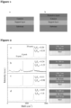
- Figure 1(a) illustrates the general composition of layers used in the prior art where catalyst is always at the top (i.e. outside) and therefore directly exposed to the hydrocarbon feedstock during the CVD process of graphene or CNTs. As previously discussed, prior to the growth process, the catalyst layer remains susceptible to environmental poisoning.
- figure 1(b) shows the general composition of the 'protected catalyst scheme' on the invention, although it will be readily understood that the catalyst and support layer could be combined into one layer.
- a catalyst is capped by a protective layer which protects the catalyst from environmental impurities prior to the growth process as well as process impurities.
- carbon radicals diffuse through the capping layer for the growth of graphene or CNTs. Growth of graphene initiates under the capping/protective layer, whereas CNTs protrude through or lift-up the capping layer.
- the grown material using the protected catalyst scheme has shown better adhesion to the substrate, suitable for many applications including corrosion resistant metal overcoats and electrically/thermally connected carbon nano-layers to the substrate.
- Graphene growth was carried out in a photo-thermal chemical vapour deposition (PTCVD) system [8-11].
- PTCVD photo-thermal chemical vapour deposition
- optical energy is delivered from the top by IR lamps situated in the head of the chamber, while the sample is placed on a water-cooled chuck.
- the top surface of a sample reaches temperature around 800°C, whereas the bulk of the sample remains below 470°C.
- the bulk temperature of a sample is recorded by a pyrometer present at the bottom side of the substrate.
- the temperature of a sample is mainly controlled by the electrical power supplied to the optical lamps, the gases used and pressure of the gases in the chamber.
- the thermal conductivity of the gases in the chamber also plays an important role in the thermal energy kinetics.
- Samples are pre-heated at 460°C (substrate bulk temperature) in flowing H 2 (100 sccm) for 10 min at 2 Torr pressure and growth of graphene is carried out for 5 min using C 2 H 2 (10 sccm) as the carbon feedstock. Samples are characterized using a Renishaw Systems 2000 Raman Spectroscope using a 514 nm laser excitation source.
- figure 2 The Raman spectra of as-grown graphene on steel substrates and corresponding layer structures is illustrated graphically in figure 2 , where figure 2 (a, c) are the spectra of graphene grown using the protected catalyst scheme, and figure 2 (b, d) are the spectra of graphene grown using generally adopted layout in the prior art.
- first order and second order Raman features are observed: the D-peaks around 1350 cm -1 , the G-peak around 1580 cm -1 and the 2D-peaks around 2700 cm1.
- the D-peak is defect induced and its intensity increases with increasing the structural defects in the material or due to the presence of amorphous carbon.
- the strongest feature in the Raman spectra is the G-peak, which is associated with the Raman-active E 2g vibrations of sp 2 bonded carbon atoms and hence, its presence is the signature of graphitization in the material.
- the intensity ratio of the G-peak and the D-peak (I D /I G ) is often used as a measure of the quality of a graphite-like material.
- the low I D /I G values (below 0.26) calculated from the Raman spectra are indicative of high structural quality of as-grown graphene.
- the quality of graphene is further improved when TiN/Al (15/10 nm) bilayers are used under Fe catalyst, as indicated by the lower I D /I G values of 0.11 and 0.05 in figure 2(c) and figure 2(d) , respectively.
- the 2D-peak is the overtone of D-peak but its intensity is independent of defects, since in this second order Raman process, both scattering events are associated with phonons, in contrary to the D-peak where one out of two scattering events is defect related.
- the shape and respective height of the 2D-peak with respect to the G-peak (I G /I 2D ) is associated to the interlayer coupling of electronic band structures and number of layers of graphene sheets, respectively.
- the I G /I 2D values in Figure 2 (a-c) are 0.24 - 1.2 which corresponds to 1 - 3 layers of graphene, whereas I G /I 2D value in Figure 2(d) is 1.6 which correspond to multilayer graphene.
- the I G /I 2D (0.24) of the sample with the catalyst-capping-layer of TiN shows the characteristics of single-layer-graphene (SLG), whereas the I G /I 2D (1.23) of the sample without the catalyst-capping layer ( figure 2(b) ) corresponds to few-layer graphene (FLG).
- the Raman spectrum of the sample given in figure 2(c) (with capping-layer) corresponds to few-layer graphene
- the spectrum given in figure 2(d) (without capping-layer) corresponds to multilayer graphene. This implies that the capping-layer (TiN) can also be utilized to limit or control the number of graphene layers.
- a narrow FWHM of 48 cm -1 and single Lorentzian shape of the 2D-peak in figure 3(b) indicates the absence of interlayer coupling of electronic band structures in FLG graphene, which is in agreement with Reina et al. [17] who stated it as a positive effect for maintaining intrinsic SLG properties in each layer of FLG.
- FIG 4 The Raman spectra of graphene grown on a Si substrate and the corresponding schematics of layer structures are illustrated in figure 4 . All spectra show well-defined Raman peaks including the D-peaks around 1345 cm -1 , the G-peaks around 1580 cm -1 and the 2D-peaks around 2700 cm -1 .
- Figure 4(a) and (c) are the Raman spectra of as-grown graphene using the protected catalyst scheme, where two catalyst materials, Fe ( figure 4(a) ) and Ni ( figure 4(c) ), are used to show the versatility of the 'protected catalyst scheme'.
- Figure 4(b) shows the Raman spectrum of the as-grown graphene using the general scheme with an Fe catalyst.
- the layer structure used for CNT growth using the protected catalyst scheme is shown in figure 5 .
- a 50 nm layer of TiN film is sputter deposited on n-Si substrate, followed by the deposition of a 10 nm Al film.
- a layer of Fe (as a catalyst) is deposited and capped by a TiN film.
- Three thicknesses of Fe films 3 nm, 6 nm and 9 nm are deposited on various samples and for each of the Fe thickness, three thicknesses of TiN films: 3.5 nm, 7 nm and 17 nm are deposited in order to demonstrate the versatility of the protected catalyst scheme. All the films on a sample are deposited sequentially in an inert gas environment without breaking vacuum. This was performed using the JLS-Design MPS 500 sputter kit, which allowed the sequential deposition of up to four metal targets in a single run without breaking vacuum. Hence, the catalyst exposure to the atmosphere is avoided in this way.
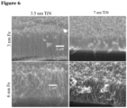
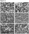
- the growth of carbon nanotubes was carried out in the PTCVD system at 2 Torr H 2 (100 sccm)/C 2 H 2 (10 sccm) pressure, in the substrate bulk temperature range of 375°C - 440°C. Heat treatment of the samples was performed first in the H 2 environment and then growth of CNTs was carried out for 5 minutes using 10 sccm of C 2 H 2 . SEM images of the CNTs grown at a substrate bulk temperature of 400°C, using the protected catalyst scheme for the samples containing 3 nm and 6 nm Fe protected by 3.5 nm and 7 nm TiN films, are shown in Figure 6 .
- Figure 7 shows the SEM micrographs of the CNTs grown as a function of temperature on 3 nm Fe protected by 3.5 - 17 nm thick TiN films.
- Figures 6 and 7 show vertically aligned and dense CNT growth for all the samples in the temperature range of 375 - 400°C. However, the vertical alignment and density of CNTs was observed to have degraded for higher temperatures (420 - 440°C), which may be because of the partial poisoning of the catalyst nanoparticles. The effect is particularly prominent on the samples containing thicker films of TiN; sparse CNTs can be observed corresponding to 17 nm TiN.
- the experiment was repeated, increasing the thickness of the Fe catalyst to 6 nm and 9 nm while keeping the remaining parameters identical.
- the SEM images for the samples containing 6 nm Fe are shown in figure 8 and the images of 9 nm Fe are shown in Figure 9 .
- the growth of CNTs for the thicker Fe films (6 nm and 9 nm) shows a nearly inverted effect with respect to temperature as compared with Figure 7 , that is, poor or no growth at lower temperature (375°C) and improved growth for higher temperatures (420 - 440°C).
- Nearly vertically aligned and relatively dense CNTs can be observed for thicker TiN capping layer (7 nm and 17 nm) at higher temperatures, in contrast with Figure 7 . This implies that the degradation of the CNT growth profile because of the partial poisoning of the catalyst can be improved by increasing the thickness of the Fe catalyst film.
- Figure 10 contains the Raman spectra of the CNTs grown on 3 nm Fe protected by the TiN film of 3.5 nm, 7 nm and 17 nm in the temperature range of 375 - 420°C.
- the SEM analysis and the presence of well-defined G-peaks along with the 2D-peaks in the Raman spectra confirm the synthesis of CNTs.
- the I D /I G ratio of 0.73 achieved in the protected catalyst scheme at substrate bulk temperature of 400°C for 3.5 nm TiN capping layer is comparable to the CNTs grown at 700°C under standard hotwall or thermal CVD growth conditions. [21, 22]
- each CNT would have been enveloped by the capping layer of TiN at its root, as illustrated in Figure 12(a) , which may be the mechanism of strong attachment of CNTs with substrate.
- FIG 12(a) may be the mechanism of strong attachment of CNTs with substrate.
- the CNTs can be grown with further increase in the thickness of TiN capping layer which may further enhance the attachment of CNTs.
- the growth of CNTs on 6 nm Fe capped with 100 nm TiN layer at 440°C is presented.
- the schematic of the layer structure is shown in Figure 13(a) , where 6 nm Fe capped with 100 nm TiN is sputter deposited over TiN/Al (50/10 nm) layers and the whole structure is patterned to 100 ⁇ 100 ⁇ m 2 squares, using a lift-off process.
- the CNT growth on this sample is carried out at 440°C (substrate bulk temperature) at 2 Torr pressure of H 2 /C 2 H 2 (100/10 sccm) using the PTCVD system.
- the as-grown CNTs are shown in Figure 13 (b - c). It can be observed in the cross-sectional SEM image of the sample given in Figure 13 (b, c) that the CNT grown square-pads remained un-cut during the cleavage of the sample with a diamond scribe which indicates their high strength.
- the strength of the pads may be because of the formation of CNT-TiN composite while CNTs were growing through the TiN capping layer.
- the catalyst deposition in high aspect ratio vias is carried out using the conventional top-down deposition scheme which not only results in the side-wall deposition but also some quantity of catalyst reaching the bottom being reduced.
- the sidewall deposition of the catalyst results in the parasitic growth of CNTs originating from the dielectric material, such as SiO 2 , which cannot take part in electrical conduction, and also hinders the growth of CNTs growing from the bottom, [18] as depicted in Figure 14(a) . Therefore, a suitable technique is required which enable the CNT growth originating only from the bottom surface of a via, as illustrated in Figure 14(b) .
- One approach (known as the buried catalyst approach) is to deposit the catalyst film before the deposition of SiO 2 and patterning.
- the protected-catalyst scheme not only provides a CMOS compatible solution to all of the above mentioned problems, but also can be a breakthrough for many potential application areas of carbon nanotubes and graphene.
- a schematic of the process flow for the fabrication of CNT-based via structures using the protected catalyst scheme and general scheme is shown in Figure 15 .
- a layer stack (M1) of Ti (30 nm), Cu (150 nm), TiN (50 nm) and Al (10 nm) is deposited as bottom metal lines on n-Si substrate.
- M1 a layer stack of Ti (30 nm), Cu (150 nm), TiN (50 nm) and Al (10 nm) is deposited as bottom metal lines on n-Si substrate.
- a 3 nm Fe catalyst is deposited over M1 followed by the deposition of a 7 nm TiN film as the protective layer of the catalyst (step 2). All these layers are deposited sequentially in a single run without breaking the vacuum.
- a 300 nm of SiO 2 film is sputter deposited and patterned lithographically to define vias on M1 (step 3).
- the catalyst Due to the protective layer of TiN the catalyst remained protected during the reactive ion etching of the SiO 2 layer which is performed for 10 minutes using CF 4 (30 sccm) and Ar (10 sccm) at 60 mTorr pressure and 100 watt RF power.
- CF 4 (30 sccm) and Ar (10 sccm) at 60 mTorr pressure and 100 watt RF power.
- a 300 nm SiO 2 film is deposited over M1, patterned lithographically and etched down to M1 (step 2). After this a 3 nm Fe catalyst is sputter deposited and photoresist then removed (step 3).
- the CNT growth is carried out in a PTCVD system using a mixture of H 2 /C 2 H 2 (100/10 sccm) at 2 Torr pressure, while the substrate bulk temperature is kept at 400°C. Catalyst heat-treatment is performed for 10 minutes at 2 Torr pressure in a H 2 environment prior to the growth of CNTs. By introducing 10 sccm C 2 H 2 , the growth of CNTs is carried out for 5 minutes (step 4). A 300 nm Al film is sputter deposited, patterned and etched as a top metal contact (not shown). Finally, electrical measurements of the CNT-based vias are performed.
- the SEM image of CNTs grown in the vias using protected catalyst scheme are shown in Figure 16(a) . Since, CNT growth occurs only from the catalyst site, all CNTs are originating from the bottom metal strips (M1), ensuring a reliable electrical contact.
- the CNTs are vertically aligned and dense ( ⁇ 10 9 cm -2 ), suitable for interconnect via application.
- the applications of patterned growth using protected catalyst scheme is not limited to the CNT-based interconnects; instead it can be used in programmable in-situ patterned growth of graphene and CNTs for various 3D structures as well as for combined graphene and CNT based horizontal and vertical interconnects.
- Figure 16(b) shows the current-voltage characteristics of 100 CNT-based vias of 10 ⁇ 10 ⁇ m 2 dimensions fabricated through protected catalyst scheme and through general scheme. Linear ohmic behaviour can be observed in both cases with a significant improvement in the conductivity of CNT-based vias fabricated through protected catalyst scheme. The improvement in the conductivity is attributed to the protection of the catalyst from environmental poisoning such as oxidation and increased number of CNTs available for conduction because of the inhibition of parasitic CNT growth from the sidewalls.
- the protected catalyst scheme can be used for the combined growth of graphene and CNTs to act as horizontal and vertical interconnects respectively, as depicted in Figure 16(c) .
- Example 5 Using different materials for the capping layer
- TiN film As a catalyst capping layer.
- TiN is not the only material that can act as a catalyst capping layer. Any material which allows the diffusion of carbon down to the catalyst can be used in the protected catalyst scheme to act as a catalyst capping layer.
- thin films of Ti, TaN, Cr, Au, Ag and Pd as a catalyst capping layer. Only growth of CNTs is demonstrated, however, it will be readily understood that this is also applicable for the graphene growth.
- Figure 17 shows a schematic of the layer structure used in this example where different materials are used as the catalyst capping layer.
- a 50 nm of TiN film is sputter deposited on n-Si substrate followed by the deposition of 10 nm Al and 3 nm Fe (catalyst), respectively.
- a film of 5 ⁇ 1 nm of Ti, TaN, Cr, Au, Ag and Pd are sputter deposited separately on different samples to act as the catalyst protective layer.
- CNT growth is carried out at 420°C (substrate bulk temperature) in a PTCVD system, using a mixture of H 2 /C 2 H 2 (100/10 sccm) at 2 Torr pressure. Catalyst heat-treatment is performed for 10 minutes in H 2 environment prior to the growth of CNTs.
- C 2 H 2 (10 sccm) is used as carbon source gas for the growth of CNTs and growth is carried out for 5 minutes.
- Raman spectra (514 nm laser wavelength) of CNTs grown on Si substrate using protected catalyst scheme where a film of 5 ⁇ 1 nm of Ti, Cr, Au, Ag, Pd and TaN is used as a catalyst capping layer are shown in Figure 19 .
- Well-defined Raman peaks can be seen in the spectra including the D-peaks around 1345 cm -1 , the G-peak around 1580 cm -1 and the 2D-peaks around 2700 cm -1 . Presence of well-developed G-peaks around 1580 cm -1 indicate that the as-deposited material (CNTs) is graphitized for all capping layer materials.
- I D /I G values indicate that the quality of the CNTs depend on the material of the capping layer.
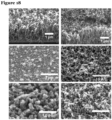
- the material and thickness of the protective layer can be selected and optimised to give various configurations to the graphene and/or CNTs to be grown. For instance, when a TiN based protective layer is used, the as-grown CNTs protrude through the TiN layer and increased adhesion of the CNTs with the substrate is observed. This is discussed in Example 3, above, and shown in Figures 11 and 13 . However, when Pd is used as the protective layer, CNT bumps wrapped with Pd are achieved as can be observed in Figure 18 . The material and thickness of the protective layer can therefore be selected to create materials with functionalities suitable for a variety of applications.
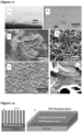
- the polyimide film was lifted-up with the growth of CNTs as schematically shown in Figure 20(b) and can be observed in the SEM image shown in Figure 20(c) , showing the cross-section of the sample (45° tilted) where the polyimide film can be seen at the top of the as-grown CNTs.
- Other polymers and plastic materials can also be used as a protective layer.
- a 3D structure is formed when the polyimide film lifts-up due to the growth of the CNTs. Accordingly, the protective layer has separated from the attachment surface due to the growth of the CNTs.
- the protective layer could comprise TiN/polyimide sublayers, where prior to CNT growth the TiN sublayer is situated adjacent to the attachment surface and the polyimide sublayer is situated adjacent to the TiN sublayer. When CNTs were grown this would cause the polyimide sublayer to lift-up and separate from the TiN sublayer, which would remain adjacent to the attachment surface.
- the TiN sublayer would improve adhesion of the CNTs, and the polyimide sublayer would form a 3D structure.
- TiN could provide the protective layer on a predefined part of the surface of the layer stack for the growth of graphene or CNTs and polyimide film could provide the protective layer over the remainder of the surface of the layer stack for the growth of CNTs.
- this approach could be combined with the catalyst protective-etching, as demonstrated in example 4. This could also allow sites to be selectively defined such that only graphene will grow and alternative sites can be defined such that only CNTs will grow. As the protective layer is lifted-up at the sites where the CNTs grow, but not at the sites where graphene grows, a 3D structure will be formed.
- CMOS complementary metal oxide semiconductors
- portions of the structure may include 3D patterning, as described above, and specific portions may be designed to grow CNTs while other portions are designed to grow graphene this technology could be used in integrated circuits and/or printed circuit boards devices and interconnects.
- Example 7 Graphene/CNT growth using thermal CVD
- the growth of graphene/CNTs using the protected catalyst scheme is not limited to a PTCVD system, instead any type of CVD can be used.
- a thermal CVD system In this system, the stage (where the sample is mounted) is heated using a resistive heating system which transfers the necessary thermal energy to the catalyst for the growth of carbon nano-materials.
- CNT growth is carried out on various samples at 700°C for 10 minutes using a mixture of C 2 H 2 /H 2 (25/200 sccm) at 10 Torr chamber pressure. Samples were pre-heated for 10 minutes in H 2 environment prior to the CNT growth. In this case the whole structure, including the substrate is heated to the temperature necessary to nucleate the carbon nano-structure.
- the layer structure is same as shown in schematic of Figure 17 where different materials are used as the catalyst protective layer.
- a 50 nm of TiN film is sputter deposited on n-Si substrate followed by the deposition of 10 nm Al and 3 nm Fe (catalyst), respectively.
- a film of 5 ⁇ 1 nm of Ti, Ta, Cr, Au, Ag and Pd are sputter deposited separately on different samples to act as the catalyst protective layer.
- SEM images of the CNTs grown using protected catalyst scheme in the thermal CVD system are shown in Figure 21 . It can be observed that different protective layers resulted in different profile of the as-grown CNTs.
- Ti based protective layer resulted in CNT bumps
- Ta resulted in sparse CNTs
- Cr resulted in dense and tangled CNTs
- Au resulted in CNT ropes
- Ag resulted in short CNT bumps
- Pd resulted in tangled CNTs.
- Raman spectra (514 nm laser wavelength) of the CNTs grown using the protected catalyst scheme in a thermal CVD system are shown in Figure 22 .
- Well-defined Raman peaks can be seen in the spectra including the D-peaks around 1345 cm -1 and the G-peak around 1580 cm -1 .
- the protective layers are Ti, Ta and Cr based
- the 2D-peaks can also be observed around 2700 cm -1 .
- Presence of well-developed G-peaks around 1580 cm -1 indicate that the as-deposited material (CNTs) is graphitized for all protective layer materials.
- the varying I D /I G values indicate that the quality of the CNTs depend on the material of the protective layer.
- Example 8 Growth of CNTs or graphene in cavities provided in the layer stack
- Figure 23a is a schematic of a layer stack provided with a cavity.
- the layer stack of Figure 23a comprises a substrate, a support layer disposed adjacent the substrate, a catalyst layer disposed adjacent the support layer, an additional layer disposed adjacent the support layer, wherein the additional layer and catalyst layer define an indentation, and a protective layer disposed adjacent the additional layer and over the indentation to form a cavity.
- the attachment surface for the CNT or graphene growth is disposed within the cavity, adjacent the catalyst layer.
- the length of the CNTs can be controlled such that CNTs extend from the attachment surface to the protective layer, but do not extend any further, as depicted in Figure 23b .
- the cavity may be under vacuum or filled with a gas.
- the cavity will be filled with an inert gas.
- Figure 24a is a schematic of an alternative embodiment of the layer stack, comprising two protective layers.
- the layer stack of Figure 24a comprises a substrate, a support layer disposed adjacent the substrate, a catalyst layer disposed adjacent the support layer, a first protective layer disposed adjacent the catalyst layer, an additional layer disposed adjacent the first protective layer, wherein the additional layer and first protective layer define an indentation, and a second protective layer disposed adjacent the additional layer and over the indentation to form a cavity.
- the attachment surface for the CNT or graphene growth is preferably disposed adjacent the catalyst layer.
- the length of the CNTs can be controlled such that CNTs extend from the attachment surface to the protective layer, but do not extend any further, as depicted in Figure 24b .
- the cavity may be under vacuum or filled with a gas.
- the cavity will be filled with an inert gas.
- Figure 25a is a schematic of a further alternative embodiment of the layer stack where the catalyst layer is provided on the opposite side of the cavity to the substrate.
- the layer stack of Figure 25a comprises a substrate, an additional layer disposed adjacent the substrate, wherein the additional layer and the substrate define an indentation, a catalyst layer disposed adjacent the additional layer and over the indentation to form a cavity, and a protective layer disposed adjacent the catalyst layer.
- the attachment surface for the CNT or graphene growth is preferably disposed within the cavity, adjacent the catalyst layer.
- the length of the CNTs can be controlled such that CNTs extend from the attachment surface to the substrate layer, but do not extend any further, as depicted in Figure 25b .
- the cavity may be under vacuum or filled with a gas.
- the cavity will be filled with an inert gas.
- Figure 26a is a schematic of a final further alternative embodiment of the layer stack where the layer stack comprises two attachment surfaces provided on opposite sides of the cavity.
- the layer stack of Figure 26a comprises a substrate, a support layer disposed adjacent to the substrate, a first catalyst layer disposed adjacent the support layer, an additional layer disposed adjacent the first catalyst layer, wherein the additional layer and first catalyst layer define an indentation, a second catalyst layer disposed adjacent the additional layer and over the indentation to form a cavity, and a protective layer disposed adjacent the second catalyst layer.
- the first attachment surface for the CNT or graphene growth is preferably disposed within the cavity, adjacent the first catalyst layer
- the second attachment surface for the CNT or graphene growth is preferably disposed with the cavity, adjacent the second catalyst layer.
- Figure 26a shows a schematic where CNTs have started to grow from the two attachment surfaces but have not yet grown to reach the opposite attachment surface. This approach could result in higher density of CNTs in the cavity.
- the cavity may be under vacuum or filled with a gas.
- the cavity will be filled with an inert gas.
- the protective layer may comprise TiN, preferably with a cross-section of around 7 nm, and/or polyimide, preferably with a cross-section of around 500 nm.
- the catalyst layer may comprise Fe, preferably with a cross-section of around 3 nm.
- the support layer may comprise two sublayers comprising TiN and Al, preferably with a cross-section of around 50 nm and10 nm respectively.
- the additional layer may comprise SiO 2 , prederably with a cross-section of around 500 nm.
- CNTs or graphene can be grown, using the methods previously discussed, such that the or each protective layer allows carbon diffusion therethrough to the or each attachment surface. Accordingly, CNTs or graphene will grow from the or each attachment surface.
- the 'protected catalyst' scheme for the growth of graphene and CNTs is demonstrated where a catalyst capping layer such as Ti, TiN, Ta, TaN, Cr, Au, Ag and Pd is used to protect the catalyst.
- the capping layer not only protects the catalyst from the environmental poisoning but also allows the diffusion of carbonaceous feedstock through it for the growth of graphene or carbon nanotubes.
- Raman spectra analysis indicates the growth of single, few and multiple layers of high quality graphene on steel and Si substrates, using the protected catalyst scheme. Vertically aligned and dense ( ⁇ 10 9 cm -2 ) growth of CNTs is also achieved using protected catalyst scheme.
- the scheme proposed can be implemented in traditional thermal CVD growth of carbon materials or other systems that allow for the coupling of energy to the catalyst along with a suitable carbon feedstock.
- the carbon feedstock could be in gas, liquid or solid form within the substrate structure proposed.
- Substrates could be pre-treated to incorporate the carbon source.
- a comparative adhesion test shows that the CNTs grown by the protected catalyst scheme are more strongly attached with the substrate surface and the strength of the attachment increases with increasing the thickness of the capping layer of TiN.
- the protected catalyst scheme is successfully used in revealing the fabrication of CNT based vias where the catalyst remained protected from etchant attack during the reactive ion etching of SiO 2 .
- the protected catalyst scheme can also be used for revealing 3D structures, patterns and simultaneous graphene-CNT growth.
- the protected catalyst scheme that has been developed is a breakthrough in many potential application areas of graphene and carbon nanotubes as it protects the catalyst from oxidation prior to the growth, maintains the high quality and high conductivity of the grown material, allows the etching of SiO 2 (or other dielectric materials) in a buried catalyst scheme while keeping the catalyst protected from etchants and improve the adhesion of graphene/CNTs on the host material.
Landscapes
- Chemical & Material Sciences (AREA)
- Organic Chemistry (AREA)
- Engineering & Computer Science (AREA)
- Materials Engineering (AREA)
- Nanotechnology (AREA)
- Inorganic Chemistry (AREA)
- General Chemical & Material Sciences (AREA)
- Chemical Kinetics & Catalysis (AREA)
- Mechanical Engineering (AREA)
- Metallurgy (AREA)
- Catalysts (AREA)
- Carbon And Carbon Compounds (AREA)
- Laminated Bodies (AREA)
Claims (14)
- Schichtstapel zum Wachsen von Graphen oder Kohlenstoffnanoröhren (CNTs), wobei der Schichtstapel ein Substrat, eine Katalysatorschicht, eine Schutzschicht und eine Anbringungsoberfläche umfasst, die zwischen der Katalysatorschicht und der Schutzschicht angeordnet ist, wobei die Katalysatorschicht in der Lage ist, das Wachstum des Graphens und/oder der CNTs zu katalysieren, dadurch gekennzeichnet, dass die Schutzschicht ein Material umfasst, das ausgewählt ist aus einer Gruppe bestehend aus: Titannitrid (TiN), Titan (Ti), Tantal (Ta), Tantalnitrid (TaN), Gold (Au), Silber (Ag), Palladium (Pd), Chrom (Cr) und einem 2D-Schichtmaterial, wobei das 2D-Schichtmaterial BN, M0S2, MoSe oder WS2 ist, zwischen 1 nm und 500 nm im Querschnitt ist und konfiguriert ist, um Kohlenstoffdiffusion dort hindurch zu der Anbringungsoberfläche zu ermöglichen, sodass Graphen oder CNTs daraus wachsen, und das Substrat ein Material umfasst, das ausgewählt ist aus einer Gruppe bestehend aus: Silizium (Si), Aluminiumoxid (Al2O3), Siliziumkarbid (SiC), Stahl, Kupfer (Cu), Nickel (Ni), Kunststoffen, Polymeren, Glas, Galliumarsenid (GaAs), Aluminium (Al) und Zeolith oder das Substrat ein Material umfasst, das mit einem 2D-Schichtmaterial beschichtet ist, das BN, MoS2 oder WS2 ist.
- Schichtstapel nach Anspruch 1, wobei die Anbringungsoberfläche für das Graphen oder die CNTs benachbart zu der Schutzschicht angeordnet ist.
- Schichtstapel nach Anspruch 1 oder Anspruch 2, wobei die Katalysatorschicht:- ein Material umfasst, das ausgewählt ist aus einer Gruppe bestehend aus: Kupfer (Cu), Nickel (Ni), Ruthenium (Ru), Kobalt (Co), Eisen (Fe), Rubidium (Rd), Platin (Pt), Iridium (Ir), Palladium (Pd), Rhodium (Rh), Karbiden, Silber (Ag), Gold (Au), Stahl oder einer Kombination aus zwei oder mehreren der vorgenannten Materialien; und/oder- zwischen 1 nm und 500 nm im Querschnitt ist.
- Schichtstapel nach einem vorhergehenden Anspruch, wobei der Schichtstapel eine Trägerschicht umfasst, die zwischen der Katalysatorschicht und dem Substrat angeordnet ist, und wobei bevorzugt die Trägerschicht ein Material umfasst, das ausgewählt ist aus einer Gruppe bestehend aus: Siliziumdioxid (SiO2), Aluminiumoxid (Al2O3), Kupfer (Cu), Aluminium (Al), Wolfram (W), Palladium (Pd), Gold (Au), Silber (Ag), Titan (Ti), Tantal (Ta), Tantalnitrid (TaN) und Titannitrid (TiN), wobei bevorzugt die Trägerschicht zumindest zwei Schichten umfasst, wobei jede Schicht eine andere Zusammensetzung umfasst, und/oder wobei die Trägerschicht zwischen 2 nm und 400 nm im Querschnitt ist.
- Schichtstapel nach einem vorhergehenden Anspruch, wobei die Schutzschicht zwischen 1 nm und 100 nm im Querschnitt oder zwischen 3,5 nm und 17 nm im Querschnitt ist.
- Schichtstapel nach einem vorhergehenden Anspruch, wobei der Schichtstapel eine zusätzliche Schicht umfasst, die zwischen dem Substrat und der Schutzschicht angeordnet ist, wobei die zusätzliche Schicht eine Vertiefung definiert und die Schutzschicht über der Vertiefung angeordnet ist, um einen Hohlraum zu bilden, und die Katalysatorschicht auf der gegenüberliegenden Seite des Hohlraums zu der Schutzschicht angeordnet ist.
- Verfahren zum Herstellen eines Schichtstapels zur Verwendung beim Wachsen von Graphen oder Kohlenstoffnanoröhren (CNTs), wobei das Verfahren Folgendes umfasst:-a) Bereitstellen eines Substrats, das ein Material umfasst, das ausgewählt ist aus einer Gruppe bestehend aus: Silizium (Si), Aluminiumoxid (Al2O3), Siliziumkarbid (SiC), Stahl, Kupfer (Cu), Nickel (Ni), Kunststoffen, Polymeren, Glas, Galliumarsenid (GaAs), Aluminium (Al) und Zeolith oder das Substrat ein Material umfasst, das mit einem 2D-Schichtmaterial beschichtet ist, wobei das 2D-Schichtmaterial BN, MoS2 oder WS2 ist, und Abscheiden einer Katalysatorschicht, die in der Lage ist, das Wachstum des Graphens und/oder der CNTs darauf zu katalysieren; undb) Abscheiden einer Schutzschicht auf der Katalysatorschicht, sodass eine Anbringungsoberfläche zwischen der Katalysatorschicht und der Schutzschicht angeordnet ist und die Katalysatorschicht zwischen dem Substrat und der Schutzschicht angeordnet ist, wodurch ein Schichtstapel erzeugt wird, wobei die Schutzschicht ein Material umfasst, das ausgewählt ist aus einer Gruppe bestehend aus: Titannitrid (TiN), Titan (Ti), Tantal (Ta), Tantalnitrid (TaN), Gold (Au), Silber (Ag), Palladium (Pd), Chrom (Cr) und einem 2D-Schichtmaterial, wobei das 2D-Schichtmaterial BN, M0S2, MoSe oder WS2 ist, zwischen 1 nm und 500 nm im Querschnitt ist und konfiguriert ist, um Kohlenstoffdiffusion dort hindurch zu der Anbringungsoberfläche zu ermöglichen, sodass Graphen oder CNTs daraus wachsen.
- Verfahren nach Anspruch 7, wobei die Katalysatorschicht und/oder Schutzschicht durch Sputtern abgeschieden, durch Clusterquellen abgeschieden, elektronenstrahlverdampft, thermisch verdampft, lösungsabgeschieden, lösungsverdampft, ionenimplantiert, spinbeschichtet, durch chemische Gasphase abgeschieden, durch Plasmagasphase abgeschieden, durch Plasmaimmersion abgeschieden oder galvanisch abgeschieden werden, wobei bevorzugt die verschiedenen Schichten nacheinander auf das Substrat in einer Inertgasumgebung durch Sputtern abgeschieden werden, ohne Vakuum zu unterbrechen.
- Verfahren zum Wachsen von Graphen oder Kohlenstoffnanoröhren (CNTs), wobei das Verfahren Folgendes umfasst:a) Bereitstellen eines Schichtstapels, der ein Substrat, eine Schutzschicht und eine Anbringungsoberfläche, die dazwischen angeordnet ist, umfasst, wobei die Schutzschicht zwischen 1 nm und 500 nm im Querschnitt ist und konfiguriert ist, um Kohlenstoffdiffusion dort hindurch zu der Anbringungsoberfläche zu ermöglichen, sodass Graphen oder CNTs daraus wachsen, dadurch gekennzeichnet, dass entweder (i) das Substrat in der Lage ist, das Wachstum von Graphen und/oder CNTs von der Anbringungsoberfläche zu katalysieren, oder (ii) der Schichtstapel ferner eine Katalysatorschicht umfasst, die zwischen dem Substrat und der Schutzschicht angeordnet ist, wobei die Anbringungsoberfläche zwischen der Katalysatorschicht und der Schutzschicht angeordnet ist und die Katalysatorschicht in der Lage ist, das Wachstum des Graphens und/oder der CNTs von der Anbringungsoberfläche zu katalysieren; undb) Anordnen des Schichtstapels in einem System zur chemischen Gasphasenabscheidung (CVD), Bereitstellen eines Kohlenstoffrohstoffes und dadurch Ermöglichen, dass Graphen oder CNTs aus der Anbringungsoberfläche wachsen.
- Verfahren nach Anspruch 9, wobei der Prozess in einem thermischen CVD(TCVD-)System, einem plasmaunterstützten CVD(PECVD-)System oder einem photothermischen CVD(PTCVD-)System durchgeführt wird, wobei bevorzugter ein PTCVD-System verwendet wird und optische Energie an den Schichtstapel geliefert wird, bevorzugt von oberhalb des Substrats.
- Verfahren nach Anspruch 9 oder Anspruch 10, wobei eine obere Oberfläche des Substrats, die mit dem Schichtstapel bereitgestellt ist, auf eine Temperatur von zumindest 500 °C, 600 °C, 700 °C oder zumindest 800 °C erhitzt wird und bevorzugt eine obere Oberfläche des Substrats, die mit dem Schichtstapel bereitgestellt ist, auf bis zu 1100 °C erhitzt wird und/oder wobei die Masse des Substrats, die mit dem Schichtstapel bereitgestellt ist, auf einer Temperatur unter 600 °C, 470 °C oder unter 250 °C bleibt.
- Verfahren nach einem der Ansprüche 9 bis 11, wobei das Wachsen von Graphen oder CNTs Vorbehandeln des Substrats auf eine Substratmassentemperatur unter 470 °C umfasst, wobei bevorzugt der Vorbehandlungsschritt wie folgt ist:- durchgeführt in strömendem Wasserstoff (H2), Argon (Ar), Stickstoff (N2), Helium (He) und/oder Ammoniak (NH3), wobei bevorzugter der/das strömende Wasserstoff (H2), Argon (Ar), Stickstoff (N2), Helium (He) und/oder Ammoniak (NH3) bei zwischen 25-500 sccm zugeführt wird;- durchgeführt bei einem Druck zwischen 13,33 Pa und 1013250 Pa, und/oder- aufrechterhalten für 1-60 Minuten, bevorzugter 5-15 Minuten, am meisten bevorzugt 10 Minuten.
- Verfahren nach einem der Ansprüche 9 bis 12, wobei Graphen wächst und die Massentemperatur des Schichtstapels zwischen 350-650 °C ist oder CNTs wächst und die Massentemperatur des Schichtstapels in dem Bereich von 250-500 °C ist und/oder wobei der Schritt des Wachsens des Graphens und/oder der CNTs 0,1-60 Minuten, bevorzugter 2-8 Minuten, am meisten bevorzugt 5 min aufrechterhalten wird.
- Verfahren nach einem der Ansprüche 9 bis 13, wobei der Kohlenstoffrohstoff ausgewählt ist aus einer Gruppe bestehend aus: Acetylen (C2H2), Ethylen (C2H4), Methan (CH4), Kohlenmonoxid (CO), Kampfer, Naphthalin, Ferrocen, Benzol und Ethanol, wobei bevorzugt der Kohlenstoffrohstoff zwischen 5-500 sccm zugeführt wird und bevorzugt bei 10 sccm zugeführt wird.
Applications Claiming Priority (2)
| Application Number | Priority Date | Filing Date | Title |
|---|---|---|---|
| GBGB1410214.9A GB201410214D0 (en) | 2014-06-09 | 2014-06-09 | A method for graphene and carbon nanotube growth |
| PCT/GB2015/051634 WO2015189575A1 (en) | 2014-06-09 | 2015-06-05 | A method for graphene and carbon nanotube growth |
Publications (3)
| Publication Number | Publication Date |
|---|---|
| EP3152158A1 EP3152158A1 (de) | 2017-04-12 |
| EP3152158C0 EP3152158C0 (de) | 2024-11-27 |
| EP3152158B1 true EP3152158B1 (de) | 2024-11-27 |
Family
ID=51266917
Family Applications (1)
| Application Number | Title | Priority Date | Filing Date |
|---|---|---|---|
| EP15728919.0A Active EP3152158B1 (de) | 2014-06-09 | 2015-06-05 | Verfahren zum graphen- und kohlenstoffnanoröhrchenwachstum |
Country Status (5)
| Country | Link |
|---|---|
| US (1) | US10385449B2 (de) |
| EP (1) | EP3152158B1 (de) |
| ES (1) | ES2998009T3 (de) |
| GB (1) | GB201410214D0 (de) |
| WO (1) | WO2015189575A1 (de) |
Families Citing this family (18)
| Publication number | Priority date | Publication date | Assignee | Title |
|---|---|---|---|---|
| TWI585237B (zh) * | 2016-01-13 | 2017-06-01 | 復盛股份有限公司 | 用於機械元件之鍍層結構及其製造方法 |
| KR101722875B1 (ko) * | 2016-04-05 | 2017-04-03 | 숭실대학교산학협력단 | MoS2/카본 나노복합체 제조방법 |
| CN106276870B (zh) * | 2016-07-27 | 2019-10-25 | 中国工程物理研究院激光聚变研究中心 | 石墨烯-碳纳米管纯碳复合薄膜的制备方法 |
| CN106751587B (zh) * | 2016-12-28 | 2019-01-11 | 深圳市明鑫高分子技术有限公司 | 石墨烯3d打印材料及其制备方法 |
| CN109423702B (zh) * | 2017-09-05 | 2021-11-19 | 中国石油化工股份有限公司 | 一种高强度、高储氢量的石墨烯基碳纤维及其制备方法 |
| JP7368363B2 (ja) | 2018-03-09 | 2023-10-24 | エーエスエムエル ネザーランズ ビー.ブイ. | グラフェンペリクルリソグラフィ装置 |
| CN108636426B (zh) * | 2018-03-22 | 2020-12-08 | 西北工业大学 | 三维有序取向二硫化钼/石墨烯高效光催化制氢复合纳米材料及制备方法 |
| FR3086673B1 (fr) * | 2018-10-01 | 2021-06-04 | Commissariat Energie Atomique | Empilement multicouche pour la croissance par cvd de nanotubes de carbone |
| CN109678138B (zh) * | 2019-01-09 | 2022-04-26 | 温州大学 | 一种单手性单壁碳纳米管的制备方法 |
| US12217958B2 (en) * | 2019-03-04 | 2025-02-04 | Samsung Electronics Co., Ltd. | Method of pre-treating substrate and method of directly forming graphene using the same |
| JP7015586B2 (ja) * | 2019-05-06 | 2022-02-15 | 浙江大学 | 吸光断熱一体化光熱蒸発材料及びその調製方法と応用 |
| WO2021133158A1 (en) * | 2019-12-23 | 2021-07-01 | Mimos Berhad | Method of forming single layer nitrogen-doped graphene |
| CN111249765B (zh) * | 2020-02-25 | 2021-04-06 | 中国科学院化学研究所 | 一种去除碳材料中金属离子的加压流体提取系统和方法 |
| CN112337614B (zh) * | 2020-10-20 | 2022-03-29 | 山东华冠智能卡有限公司 | 一种石墨烯母料研磨剥离装置 |
| WO2022101210A2 (en) * | 2020-11-10 | 2022-05-19 | B2D Holding Gmbh | Three-dimensional high aspect ratio graphene film composites |
| CN112978715A (zh) * | 2021-02-24 | 2021-06-18 | 苏州大学 | 一种以醇类溶剂为碳源的碳纳米管及其制备方法 |
| CN115304055B (zh) * | 2022-08-24 | 2023-11-24 | 广东能源集团科学技术研究院有限公司 | 一种聚乙烯类废塑料的回收方法及其制备的碳纳米管 |
| KR102764657B1 (ko) * | 2023-10-06 | 2025-02-07 | (주)티에스아이 | 탄소나노튜브 제조용 촉매의 제조 방법 및 탄소나노튜브의 제조 방법 |
Family Cites Families (10)
| Publication number | Priority date | Publication date | Assignee | Title |
|---|---|---|---|---|
| EP2038262B1 (de) | 2006-05-25 | 2014-11-12 | Synta Pharmaceuticals Corp. | Die hsp90-aktivität modulierende triazolverbindungen |
| US20090011241A1 (en) * | 2007-07-07 | 2009-01-08 | College Of William And Mary | Carbon Nanoflake Compositions and Methods of Production |
| US20100221526A1 (en) * | 2007-09-18 | 2010-09-02 | Shimane Prefectural Government | Metal-coated carbon material and carbon-metal composite material using the same |
| FR2937343B1 (fr) | 2008-10-17 | 2011-09-02 | Ecole Polytech | Procede de croissance controlee de film de graphene |
| US8507797B2 (en) | 2009-08-07 | 2013-08-13 | Guardian Industries Corp. | Large area deposition and doping of graphene, and products including the same |
| US20140120270A1 (en) * | 2011-04-25 | 2014-05-01 | James M. Tour | Direct growth of graphene films on non-catalyst surfaces |
| CN102849961B (zh) | 2011-07-01 | 2016-08-03 | 中央研究院 | 在基板上成长碳薄膜或无机材料薄膜的方法 |
| FR2982853B1 (fr) | 2011-11-22 | 2018-01-12 | Ecole Polytechnique | Procede de fabrication de film de graphene |
| TWI448427B (zh) * | 2012-02-08 | 2014-08-11 | Nat Univ Tsing Hua | 利用低頻電磁波製備石墨烯之方法 |
| US9656246B2 (en) | 2012-07-11 | 2017-05-23 | Carbice Corporation | Vertically aligned arrays of carbon nanotubes formed on multilayer substrates |
-
2014
- 2014-06-09 GB GBGB1410214.9A patent/GB201410214D0/en not_active Ceased
-
2015
- 2015-06-05 ES ES15728919T patent/ES2998009T3/es active Active
- 2015-06-05 US US15/317,562 patent/US10385449B2/en active Active
- 2015-06-05 EP EP15728919.0A patent/EP3152158B1/de active Active
- 2015-06-05 WO PCT/GB2015/051634 patent/WO2015189575A1/en not_active Ceased
Also Published As
| Publication number | Publication date |
|---|---|
| US10385449B2 (en) | 2019-08-20 |
| GB201410214D0 (en) | 2014-07-23 |
| US20170121177A1 (en) | 2017-05-04 |
| EP3152158C0 (de) | 2024-11-27 |
| ES2998009T3 (en) | 2025-02-18 |
| WO2015189575A1 (en) | 2015-12-17 |
| EP3152158A1 (de) | 2017-04-12 |
Similar Documents
| Publication | Publication Date | Title |
|---|---|---|
| EP3152158B1 (de) | Verfahren zum graphen- und kohlenstoffnanoröhrchenwachstum | |
| Yeh et al. | Single-step growth of graphene and graphene-based nanostructures by plasma-enhanced chemical vapor deposition | |
| Paul et al. | Synthesis of a pillared graphene nanostructure: a counterpart of three‐dimensional carbon architectures | |
| Zeng et al. | “White graphenes”: boron nitride nanoribbons via boron nitride nanotube unwrapping | |
| Zhao et al. | Self-limiting chemical vapor deposition growth of monolayer graphene from ethanol | |
| Byun et al. | Graphenes converted from polymers | |
| Su et al. | High-quality thin graphene films from fast electrochemical exfoliation | |
| Van Khai et al. | Influence of N-doping on the structural and photoluminescence properties of graphene oxide films | |
| Kim et al. | Growth of high-crystalline, single-layer hexagonal boron nitride on recyclable platinum foil | |
| Zou et al. | Carbide-forming groups IVB-VIB metals: a new territory in the periodic table for CVD growth of graphene | |
| Soin et al. | Enhanced and stable field emission from in situ nitrogen-doped few-layered graphene nanoflakes | |
| Chen et al. | Synthesis and characterization of large-area graphene and graphite films on commercial Cu–Ni alloy foils | |
| KR101622306B1 (ko) | 그라펜 시트, 이를 포함하는 그라펜 기재 및 그의 제조방법 | |
| Huang et al. | Substrate engineering for CVD growth of single crystal graphene | |
| Nguyen et al. | Atomically thin epitaxial template for organic crystal growth using graphene with controlled surface wettability | |
| Asif et al. | Thickness controlled water vapors assisted growth of multilayer graphene by ambient pressure chemical vapor deposition | |
| Kumar et al. | Chemical vapor deposition of carbon nanotubes on monolayer graphene substrates: reduced etching via suppressed catalytic hydrogenation using C2H4 | |
| Kwon et al. | Value‐added recycling of inexpensive carbon sources to graphene and carbon nanotubes | |
| Kaur et al. | Transfer-free graphene growth on dielectric substrates: A review of the growth mechanism | |
| Innis et al. | Borophene bottom-up syntheses: a critical review | |
| Josline et al. | Recent advances in the low-temperature chemical vapor deposition growth of graphene | |
| Jun | Fundamental of graphene | |
| Ahmad et al. | Protected catalyst growth of graphene and carbon nanotubes | |
| Jeong et al. | Electron‐transfer transparency of graphene: Fast reduction of metal ions on graphene‐covered donor surfaces | |
| Yokoyama et al. | Low-temperature synthesis of multiwalled carbon nanotubes by graphite antenna CVD in a hydrogen-free atmosphere |
Legal Events
| Date | Code | Title | Description |
|---|---|---|---|
| STAA | Information on the status of an ep patent application or granted ep patent |
Free format text: STATUS: THE INTERNATIONAL PUBLICATION HAS BEEN MADE |
|
| PUAI | Public reference made under article 153(3) epc to a published international application that has entered the european phase |
Free format text: ORIGINAL CODE: 0009012 |
|
| STAA | Information on the status of an ep patent application or granted ep patent |
Free format text: STATUS: REQUEST FOR EXAMINATION WAS MADE |
|
| 17P | Request for examination filed |
Effective date: 20161220 |
|
| AK | Designated contracting states |
Kind code of ref document: A1 Designated state(s): AL AT BE BG CH CY CZ DE DK EE ES FI FR GB GR HR HU IE IS IT LI LT LU LV MC MK MT NL NO PL PT RO RS SE SI SK SM TR |
|
| AX | Request for extension of the european patent |
Extension state: BA ME |
|
| DAV | Request for validation of the european patent (deleted) | ||
| DAX | Request for extension of the european patent (deleted) | ||
| STAA | Information on the status of an ep patent application or granted ep patent |
Free format text: STATUS: EXAMINATION IS IN PROGRESS |
|
| 17Q | First examination report despatched |
Effective date: 20180627 |
|
| GRAP | Despatch of communication of intention to grant a patent |
Free format text: ORIGINAL CODE: EPIDOSNIGR1 |
|
| STAA | Information on the status of an ep patent application or granted ep patent |
Free format text: STATUS: GRANT OF PATENT IS INTENDED |
|
| INTG | Intention to grant announced |
Effective date: 20240321 |
|
| GRAS | Grant fee paid |
Free format text: ORIGINAL CODE: EPIDOSNIGR3 |
|
| GRAA | (expected) grant |
Free format text: ORIGINAL CODE: 0009210 |
|
| STAA | Information on the status of an ep patent application or granted ep patent |
Free format text: STATUS: THE PATENT HAS BEEN GRANTED |
|
| AK | Designated contracting states |
Kind code of ref document: B1 Designated state(s): AL AT BE BG CH CY CZ DE DK EE ES FI FR GB GR HR HU IE IS IT LI LT LU LV MC MK MT NL NO PL PT RO RS SE SI SK SM TR |
|
| REG | Reference to a national code |
Ref country code: GB Ref legal event code: FG4D |
|
| REG | Reference to a national code |
Ref country code: CH Ref legal event code: EP |
|
| REG | Reference to a national code |
Ref country code: IE Ref legal event code: FG4D |
|
| REG | Reference to a national code |
Ref country code: DE Ref legal event code: R096 Ref document number: 602015090497 Country of ref document: DE |
|
| U01 | Request for unitary effect filed |
Effective date: 20241217 |
|
| U07 | Unitary effect registered |
Designated state(s): AT BE BG DE DK EE FI FR IT LT LU LV MT NL PT RO SE SI Effective date: 20250110 |
|
| REG | Reference to a national code |
Ref country code: ES Ref legal event code: FG2A Ref document number: 2998009 Country of ref document: ES Kind code of ref document: T3 Effective date: 20250218 |
|
| PG25 | Lapsed in a contracting state [announced via postgrant information from national office to epo] |
Ref country code: HR Free format text: LAPSE BECAUSE OF FAILURE TO SUBMIT A TRANSLATION OF THE DESCRIPTION OR TO PAY THE FEE WITHIN THE PRESCRIBED TIME-LIMIT Effective date: 20241127 Ref country code: IS Free format text: LAPSE BECAUSE OF FAILURE TO SUBMIT A TRANSLATION OF THE DESCRIPTION OR TO PAY THE FEE WITHIN THE PRESCRIBED TIME-LIMIT Effective date: 20250327 |
|
| PG25 | Lapsed in a contracting state [announced via postgrant information from national office to epo] |
Ref country code: NO Free format text: LAPSE BECAUSE OF FAILURE TO SUBMIT A TRANSLATION OF THE DESCRIPTION OR TO PAY THE FEE WITHIN THE PRESCRIBED TIME-LIMIT Effective date: 20250227 |
|
| PG25 | Lapsed in a contracting state [announced via postgrant information from national office to epo] |
Ref country code: GR Free format text: LAPSE BECAUSE OF FAILURE TO SUBMIT A TRANSLATION OF THE DESCRIPTION OR TO PAY THE FEE WITHIN THE PRESCRIBED TIME-LIMIT Effective date: 20250228 |
|
| PG25 | Lapsed in a contracting state [announced via postgrant information from national office to epo] |
Ref country code: PL Free format text: LAPSE BECAUSE OF FAILURE TO SUBMIT A TRANSLATION OF THE DESCRIPTION OR TO PAY THE FEE WITHIN THE PRESCRIBED TIME-LIMIT Effective date: 20241127 |
|
| PG25 | Lapsed in a contracting state [announced via postgrant information from national office to epo] |
Ref country code: RS Free format text: LAPSE BECAUSE OF FAILURE TO SUBMIT A TRANSLATION OF THE DESCRIPTION OR TO PAY THE FEE WITHIN THE PRESCRIBED TIME-LIMIT Effective date: 20250227 |
|
| PG25 | Lapsed in a contracting state [announced via postgrant information from national office to epo] |
Ref country code: SM Free format text: LAPSE BECAUSE OF FAILURE TO SUBMIT A TRANSLATION OF THE DESCRIPTION OR TO PAY THE FEE WITHIN THE PRESCRIBED TIME-LIMIT Effective date: 20241127 |
|
| PGFP | Annual fee paid to national office [announced via postgrant information from national office to epo] |
Ref country code: GB Payment date: 20250619 Year of fee payment: 11 |
|
| PG25 | Lapsed in a contracting state [announced via postgrant information from national office to epo] |
Ref country code: SK Free format text: LAPSE BECAUSE OF FAILURE TO SUBMIT A TRANSLATION OF THE DESCRIPTION OR TO PAY THE FEE WITHIN THE PRESCRIBED TIME-LIMIT Effective date: 20241127 |
|
| PG25 | Lapsed in a contracting state [announced via postgrant information from national office to epo] |
Ref country code: CZ Free format text: LAPSE BECAUSE OF FAILURE TO SUBMIT A TRANSLATION OF THE DESCRIPTION OR TO PAY THE FEE WITHIN THE PRESCRIBED TIME-LIMIT Effective date: 20241127 |
|
| U20 | Renewal fee for the european patent with unitary effect paid |
Year of fee payment: 11 Effective date: 20250620 |
|
| PLBE | No opposition filed within time limit |
Free format text: ORIGINAL CODE: 0009261 |
|
| STAA | Information on the status of an ep patent application or granted ep patent |
Free format text: STATUS: NO OPPOSITION FILED WITHIN TIME LIMIT |
|
| REG | Reference to a national code |
Ref country code: CH Ref legal event code: L10 Free format text: ST27 STATUS EVENT CODE: U-0-0-L10-L00 (AS PROVIDED BY THE NATIONAL OFFICE) Effective date: 20251008 |
|
| PGFP | Annual fee paid to national office [announced via postgrant information from national office to epo] |
Ref country code: ES Payment date: 20250718 Year of fee payment: 11 |
|
| 26N | No opposition filed |
Effective date: 20250828 |
|
| REG | Reference to a national code |
Ref country code: CH Ref legal event code: H13 Free format text: ST27 STATUS EVENT CODE: U-0-0-H10-H13 (AS PROVIDED BY THE NATIONAL OFFICE) Effective date: 20260127 |
|
| PG25 | Lapsed in a contracting state [announced via postgrant information from national office to epo] |
Ref country code: MC Free format text: LAPSE BECAUSE OF FAILURE TO SUBMIT A TRANSLATION OF THE DESCRIPTION OR TO PAY THE FEE WITHIN THE PRESCRIBED TIME-LIMIT Effective date: 20241127 |
|
| PG25 | Lapsed in a contracting state [announced via postgrant information from national office to epo] |
Ref country code: IE Free format text: LAPSE BECAUSE OF NON-PAYMENT OF DUE FEES Effective date: 20250605 |
|
| PG25 | Lapsed in a contracting state [announced via postgrant information from national office to epo] |
Ref country code: CH Free format text: LAPSE BECAUSE OF NON-PAYMENT OF DUE FEES Effective date: 20250630 |