EP3155662B1 - Struktur einer ausleseschaltung mit ladungsinjektion - Google Patents
Struktur einer ausleseschaltung mit ladungsinjektion Download PDFInfo
- Publication number
- EP3155662B1 EP3155662B1 EP15729435.6A EP15729435A EP3155662B1 EP 3155662 B1 EP3155662 B1 EP 3155662B1 EP 15729435 A EP15729435 A EP 15729435A EP 3155662 B1 EP3155662 B1 EP 3155662B1
- Authority
- EP
- European Patent Office
- Prior art keywords
- substrate
- doped region
- type
- diode
- charges
- Prior art date
- Legal status (The legal status is an assumption and is not a legal conclusion. Google has not performed a legal analysis and makes no representation as to the accuracy of the status listed.)
- Active
Links
Images


Classifications
-
- H—ELECTRICITY
- H10—SEMICONDUCTOR DEVICES; ELECTRIC SOLID-STATE DEVICES NOT OTHERWISE PROVIDED FOR
- H10F—INORGANIC SEMICONDUCTOR DEVICES SENSITIVE TO INFRARED RADIATION, LIGHT, ELECTROMAGNETIC RADIATION OF SHORTER WAVELENGTH OR CORPUSCULAR RADIATION
- H10F39/00—Integrated devices, or assemblies of multiple devices, comprising at least one element covered by group H10F30/00, e.g. radiation detectors comprising photodiode arrays
- H10F39/80—Constructional details of image sensors
- H10F39/809—Constructional details of image sensors of hybrid image sensors
-
- H—ELECTRICITY
- H04—ELECTRIC COMMUNICATION TECHNIQUE
- H04N—PICTORIAL COMMUNICATION, e.g. TELEVISION
- H04N25/00—Circuitry of solid-state image sensors [SSIS]; Control thereof
- H04N25/60—Noise processing, e.g. detecting, correcting, reducing or removing noise
- H04N25/616—Noise processing, e.g. detecting, correcting, reducing or removing noise involving a correlated sampling function, e.g. correlated double sampling [CDS] or triple sampling
-
- H—ELECTRICITY
- H04—ELECTRIC COMMUNICATION TECHNIQUE
- H04N—PICTORIAL COMMUNICATION, e.g. TELEVISION
- H04N25/00—Circuitry of solid-state image sensors [SSIS]; Control thereof
- H04N25/60—Noise processing, e.g. detecting, correcting, reducing or removing noise
- H04N25/65—Noise processing, e.g. detecting, correcting, reducing or removing noise applied to reset noise, e.g. KTC noise related to CMOS structures by techniques other than CDS
-
- H—ELECTRICITY
- H04—ELECTRIC COMMUNICATION TECHNIQUE
- H04N—PICTORIAL COMMUNICATION, e.g. TELEVISION
- H04N25/00—Circuitry of solid-state image sensors [SSIS]; Control thereof
- H04N25/70—SSIS architectures; Circuits associated therewith
- H04N25/76—Addressed sensors, e.g. MOS or CMOS sensors
- H04N25/77—Pixel circuitry, e.g. memories, A/D converters, pixel amplifiers, shared circuits or shared components
-
- H—ELECTRICITY
- H04—ELECTRIC COMMUNICATION TECHNIQUE
- H04N—PICTORIAL COMMUNICATION, e.g. TELEVISION
- H04N25/00—Circuitry of solid-state image sensors [SSIS]; Control thereof
- H04N25/70—SSIS architectures; Circuits associated therewith
- H04N25/76—Addressed sensors, e.g. MOS or CMOS sensors
- H04N25/78—Readout circuits for addressed sensors, e.g. output amplifiers or A/D converters
-
- H—ELECTRICITY
- H10—SEMICONDUCTOR DEVICES; ELECTRIC SOLID-STATE DEVICES NOT OTHERWISE PROVIDED FOR
- H10F—INORGANIC SEMICONDUCTOR DEVICES SENSITIVE TO INFRARED RADIATION, LIGHT, ELECTROMAGNETIC RADIATION OF SHORTER WAVELENGTH OR CORPUSCULAR RADIATION
- H10F39/00—Integrated devices, or assemblies of multiple devices, comprising at least one element covered by group H10F30/00, e.g. radiation detectors comprising photodiode arrays
- H10F39/10—Integrated devices
- H10F39/12—Image sensors
- H10F39/18—Complementary metal-oxide-semiconductor [CMOS] image sensors; Photodiode array image sensors
-
- H—ELECTRICITY
- H10—SEMICONDUCTOR DEVICES; ELECTRIC SOLID-STATE DEVICES NOT OTHERWISE PROVIDED FOR
- H10F—INORGANIC SEMICONDUCTOR DEVICES SENSITIVE TO INFRARED RADIATION, LIGHT, ELECTROMAGNETIC RADIATION OF SHORTER WAVELENGTH OR CORPUSCULAR RADIATION
- H10F39/00—Integrated devices, or assemblies of multiple devices, comprising at least one element covered by group H10F30/00, e.g. radiation detectors comprising photodiode arrays
- H10F39/011—Manufacture or treatment of image sensors covered by group H10F39/12
- H10F39/021—Manufacture or treatment of image sensors covered by group H10F39/12 of image sensors having active layers comprising only Group III-V materials, e.g. GaAs, AlGaAs or InP
-
- H—ELECTRICITY
- H10—SEMICONDUCTOR DEVICES; ELECTRIC SOLID-STATE DEVICES NOT OTHERWISE PROVIDED FOR
- H10W—GENERIC PACKAGES, INTERCONNECTIONS, CONNECTORS OR OTHER CONSTRUCTIONAL DETAILS OF DEVICES COVERED BY CLASS H10
- H10W90/00—Package configurations
- H10W90/701—Package configurations characterised by the relative positions of pads or connectors relative to package parts
- H10W90/721—Package configurations characterised by the relative positions of pads or connectors relative to package parts of bump connectors
- H10W90/724—Package configurations characterised by the relative positions of pads or connectors relative to package parts of bump connectors between a chip and a stacked insulating package substrate, interposer or RDL
Definitions
- the invention relates to a read circuit structure for an electromagnetic sensor.
- electromagnetic sensor is meant in this text an electromagnetic radiation sensor composed of pixel reading circuits, each pixel comprising at least one photodiode for emitting an electrical signal representative of the radiation to which the pixel is exposed.
- a sensor is made from a semiconductor substrate (for example made of silicon) in which the photodiodes are constituted.
- the radiation that one seeks to exploit may for example be a radiation in the visible spectrum, however this is not limiting.
- the electrical signal emitted by each photodiode is read by a read circuit (generally a respective read circuit is dedicated to each photodiode for this purpose).
- the reading circuits are also constituted in the silicon semiconductor substrate.
- the invention finds an advantageous application in hybrid sensors.
- a sensor is said to be "hybrid" when the photodiodes are constituted in a first distinct substrate of a second substrate which integrates the reading circuits and whose semiconductor material may differ from the material of the first substrate.
- the reading circuits are constituted in a silicon substrate (which corresponds to the most common configuration for these read circuits), whereas the photodiodes are often constituted in a substrate in another material, for example gallium-indium arsenide (InGaAs), which makes it possible to constitute photodiodes sensitive to wavelengths adapted to night vision, to which a photodiode in a silicon substrate is not sensitive.
- InGaAs gallium-indium arsenide
- each photodiode of the first substrate is connected to a reading circuit of the second substrate by a weld type connection, for example an indium ball.
- a weld type connection for example an indium ball.
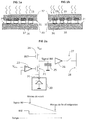
- the Figures 1a and 1b show examples of possible configurations of this hybridization, according to the flip chip technique. According to this technique, the face 31 of the first substrate 32 at which the photodiodes 33 are made, and the face 34 of the second substrate 35 at which the read circuit 36 is formed, face each other.
- each of the photodiodes 33 of the first substrate 32 is connected to the reading circuit 36 by an indium ball 37
- the connection is made by a copper pillar 38 starting from the second substrate 35 and by a weld 39 between this pillar 38 and the photodiode 33.
- the reading of the signals from the photodiodes is performed at a given frequency, which is generally the same frequency for all photodiodes.
- the frequency can be 50 or 60 Hertz.
- the frequency is higher.
- the reading of the photodiodes is thus done by "cycles", each cycle corresponding to the integration time of the pixel, that is to say the time during which the electric charge (constituted by the charges of the electrons or holes, according to the nature of the photodiode) generated by the photodiode is accumulated either in the photodiode or in the reading circuit, as well as in the reading time of the pixel.
- the reading circuit of the photodiode can be realized in different ways, in a CMOS technology. It can be in particular of the "direct injection” (DI for Direct Injection) type, “capacitive trans-impedance amplification” (CTIA for "Capacitive Trans-Impedance Amplifier” in English), or “follower of source per pixel” ( SFP for “Source Follower per Pixel”).
- DI Direct Injection
- CTIA Capacitive trans-impedance amplification
- SFP Source follower per Pixel
- the figure 2a illustrates an exemplary circuit diagram of a direct injection type pixel read circuit in a hybrid configuration.
- An amplifier 23 associated with a transistor 22 stabilizes the bias voltage applied to the photodiode 20 via the hybridization contact 21 between the first substrate on which the photodiode 20 is made and the second substrate on which the reading circuit is made.
- An initialization transistor 24 is controlled by an initialization signal RST to apply an initialization voltage V RST at the output of the transistor 22.
- An integration capacitor 25 is adapted to integrate the photo-current emitted by the photodiode 20.
- a buffer amplifier 26 makes it possible to send the signal voltage IM at the terminals of this integration capacitor 25 to a scanning multiplexing bus 28 via a selection switch 27.
- the result of the reading can either be output directly from the reading circuit to be exploited, or be stored in a memory present in each pixel for later use.
- KTC K denoting the Boltzmann constant
- T the temperature in Kelvin
- C the capacitance of the integration capacitor 25, with reference to the magnitudes influencing this sound.
- the residual charge in the integration capacitor 25 has a random variation whose root mean square is KTC .
- this KTC noise results in a deviation error of the voltage at the terminals of the integration capacitor 25 with respect to the reset voltage V RST .
- CDS Correlated Double Sampling
- a first reading is performed at the beginning of the cycle, immediately after the capacitor has been put back into an initial state (reset or 'reset' in English - a term that will sometimes be used for convenience and which must be considered equivalent), by a setting to a reference potential.
- This first reading gives a first read value of the amount of initial charges in the capacitor.
- the second reading is performed at the end of the cycle, when the capacitor is charged and it is desired to read the value of the cumulative integrated charges.
- comparison and calculation means establish the difference between the two read values. This difference gives the amount of charges generated by the photodiode that has been integrated by the capacitor during the integration time.
- circuits and methods of known types thus make it possible to determine, by calculating the difference between a cycle start reading and an end of cycle reading, for each photodiode and for each cycle, a value of the quantity of charges integrated into the circuit. capacitor from the photodiode during the integration cycle.
- CMOS complementary Metal Oxide Semiconductor
- 1 / f the dominant noise in all active components such as transistors.
- the power spectral density of this 1 / f noise decreases with frequency.
- the noise 1 / f is important.
- the frequency of the pixel operating cycles is of the order of 50 Hz, which results in a significant noise 1 / f which limits the effectiveness of the correlated double-reading.
- CTIA capacitive Trans-impedance Amplifier
- the principle is similar to that of a direct injection circuit, with similar elements designated by the same reference numerals.
- the photocurrent from the photodiode 20 is integrated in the capacitor 25 through an operational amplifier 29 provided with a capacitive feedback.
- the initialization is done by emptying the charges in the capacitor 25 by means of the initialization transistor 24 connected in parallel.
- the bias voltage of the photodiode 20 is maintained thanks to the high gain of the operational amplifier 29.
- the basic principle of this configuration is that the capacitive feedback reduces the low frequency noise and thus improves the efficiency of the correlated double reading.
- the reading sequence is the same as that of a direct injection pixel: a first reading is made after the reset and a second reading is made after the integration time, the image signal being constituted by the difference between these two readings.
- the noise 1 / f remains important.
- the best CTIA reading circuits can not fall below a noise level corresponding to the charge of 40 to 50 electrons, for a very low capacitance value (5 to 10 fF).
- the dynamics of the circuit is very low, and it saturates easily when the light exposure becomes too great.
- SFP for the English “Source follower per Pixel”, source follower by pixel, whose Figure 2c shows an exemplary embodiment.
- This configuration aims to reduce the number of transistors to reduce the number of sources of noise 1 / f.
- the operating cycle is the same as a pixel read circuit Di or CTIA, and the elements similar to these circuits are designated by the same reference numerals.
- SFP pixel readout circuit integration of the photo-current from the photodiode 20 is performed directly on the photodiode integration capacitor 25, including some parasitic capacitances.
- the high capacitive value of the photodiode 20 reduces the amplitude of the signal read in voltage.
- the noise of the reading circuit finally limits the level of noise reported to the photodiode 20 as the number of electrons.
- a CTIA pixel readout circuit can operate with a capacity of 5 fF for the integration capacitor, and for a read noise of 320 ⁇ V amplitude, the noise level is thus equivalent to the electric charge of 10 electrons.
- the integration capability can hardly be less than 20 fF. In this case, the reading noise of 320 ⁇ V results in a noise equivalent to 40 electrons.
- Another drawback for the correlated double reading in each of these circuits is that the first reading takes place at the beginning of the integration cycle, while the second reading takes place at the end of it.
- the two readings are separated by a long enough time, comparable to the cycle time.
- the time separating the two readings of each cycle corresponds to the integration time, which is equal to the cycle time (to the reset time).
- other electronic noise than the KTC noise can disturb the measurement, like the noise 1 / f, which can thus, by its variations between the two readings, lead to values of loads (deduced from the difference of the two values read) erroneous. This is penalizing and will be even more so as the cycle time is long, corresponding to low frequencies.
- an application particularly penalized by this limitation is the low light vision, which requires long cycle times, with frequencies of the order of 50 Hz.
- the invention aims to overcome these limitations and disadvantages.
- a reading circuit structure as defined in claim 1 is provided.
- the invention relates to a method for operating a read circuit structure according to claim 13.
- the invention also relates to a matrix reading circuit comprising a plurality of read circuit structures according to the invention.
- the invention also relates to a hybrid sensor comprising a first substrate on which is formed a read circuit according to the invention, and a second substrate on which is formed a matrix of elements sensitive to electromagnetic radiation constituting the external charge sources, of the photodiodes.
- the read circuit and the array of sensitive elements can be connected by a link in a configuration according to the flip-chip technique.
- the read circuit structure is formed on a P type semiconductor substrate 1 (P-sub).
- the substrate 1 has different doped regions constituting elements of the read circuit structure.
- the active read circuit structure is intended to measure the charges received from a source of charges 2 outside the substrate 1.
- This source of charges 2 is a photodiode formed on a second substrate different from the substrate 1 on which is realized the read circuit structure.
- this external source of charges 2 can be made on a second substrate, as in hybrid configurations of the type illustrated by FIGS. Figures 1a and 1b .
- the external source of charge 2 could also be a current source of a type other than a photodiode.
- a PN junction is formed in a first doped region 4 of the substrate 1 to receive electrical charges from the external charge source 2 to the substrate 1.
- the first doped region 4 of the substrate is N-doped.
- the charge source 2 is connected to the injection PN junction 4, for example via a hybridization contact 3 formed by a weld type bond, as in the examples of Figures 1a and 1b .
- the PN junction thus receives the electric current generated by the charge source 2 outside the substrate 1.
- the first PN junction is forward biased so that the charges received from the charge source 2 outside the substrate 1 can be injected into the substrate 1.
- the first PN junction thus constitutes a diode for injecting charges into the substrate 1.
- injection of the charges into the substrate 1 by the injection diode is represented by arrows in dashes on the figure 3 . Thereafter, there will be no distinction made between the diode and the doped region which constitutes with the substrate a PN junction.
- the injected charges are electrons, and the number of free electrons thus injected into the substrate 1 is proportional to the product between the duration of injection and the electric current flowing between the photodiode 2 and the first doped region 4.
- the read circuit structure comprises a second PN junction comprising a second doped region 6 of the second type, buried in the substrate, and forming therewith a buried collection diode, able to collect in the substrate 1 at least a portion of the injected by the injection diode and accumulating these charges during a charge integration cycle.
- the distance between the second doped region 6 and the first doped region 4 is less than the electron diffusion length in the substrate 1 at a nominal use temperature, for example at 20 ° C., and is preferably less than 150 ⁇ m. .
- the charges are injected into the substrate 1 at the first doped region 4 and diffuse into said substrate 1.
- the charges are then collected by the second doped region 6.
- the injected charges pass through the depth of the substrate 1 to be collected by the second doped region.
- the PN junction formed around this buried second doped region 6 and the depth of penetration of the depletion zone therein depends on the doping and the polarization voltage of the second doped region 6.
- the depletion zone invades all of this second doped region 6, there are no more mobile charges, that is to say more free electrons in the case of a second doped region 6 type N.
- the only remaining charge in this second doped region 6 is then the fixed charge, positive in the case of a second type N, left by the doping atoms.
- the second doped region 6 is buried in the substrate 1 so that the space charge area (also called depletion zone) of the junction between said second doped region 6 and the substrate 1 does not reach the surface of the substrate 1 when said doped region 6 is devoid of moving charges.
- a doping surface area 5 of the first type, in this case P may be provided between the doped region 6 of the buried collection diode and the surface of the substrate 1, in order to prevent the depletion zone reach this surface.
- the potential of the second doped region 6 no longer varies, but can still attract mobile charge carriers, in this case electrons in the case of a second N-doped region. carriers of free charges are generated or injected near this second doped region 6, they can be attracted and fixed there. The second doped region 6 can then act as an integrator without any initial residual charge. In the initial state after the charge transfer, the potential at which the second doped region 6 is subjected is maximum, and decreases as the charges injected by the injection diode are collected.
- the second doped region 6 of the second type composing the buried collection diode is configured (via its positioning, its dimensions and the dopant concentrations) to be completely depleted at the end of the charge transfer to the recovery structure. loads. It should be noted moreover that the completely depleted aspect of the second doped region 6 of the buried collection diode makes it possible to suppress the KTC noise.
- the read circuit structure also includes a charge recovery structure configured to recover charges accumulated in said collection diode.
- this recovery structure may comprise a floating diffusion node 7 formed by an N-type doped region in the substrate 1, connected to an output device 8, said N-type doped region having a dopant concentration greater than that of the second N-type doped region 6 forming with the substrate 1 the buried collection diode.
- the charge recovery structure also comprises an MOS transfer transistor whose transfer gate 9 is located between said buried collection diode and said floating diffusion node 7.
- the gate 9 is above and electrically isolated from the substrate 1 and can be controlled by a transfer signal TX to transfer the charges that are accumulated in the second doped region 6 of the buried diode to the charge recovery structure, here the floating diffusion node 7.
- the charge recovery structure may also comprise a memory constituted by a doped region of the second type, ie N, formed in the substrate 1 between the buried collection diode and the floating diffusion node 7 connected to the output device 8.
- This doped region 15 is buried as the second doped region 6, and for this purpose a doping surface area of the first type, ie P, isolates said doped region 15 from the surface of the substrate 1.
- a transistor gate 16 controlled by a signal T1 can control the transfer of charges from the buried collection diode to the memory, while the gate 9 of the transfer transistor serves to control the transfer of charges from the memory to the floating broadcast node 7.
- the memory has an N-type dopant concentration greater than that of the second doped region 6, but less than that of the floating diffusion node 7, in order to present a n potential gradient to allow the transfer of loads.
- Several memories may be arranged in a similar manner between the buried collection diode and the floating diffusion node 7 connected to the output device 8.
- the output device 8 through which the output signal resulting from the reading of the voltage at the charge recovery structure may pass, may comprise an amplifier 26 and a selection switch 27 connected to the amplifier 26, said selectively selectable selector switch 27 for connecting the output of the amplifier 26 to a multiplexing bus 28.
- the read circuit structure also includes means for initializing the charge recovery structure prior to charge transfer, returning the electrical potential of said charge recovery structure to an initial potential greater than the potential at which the second doped region 6 is completely depleted (called "pinning voltage” in English), so that when the gate 9 of the transfer transistor allows the transfer of accumulated charges in the second doped region 6 of the buried diode.
- the means for initializing the charge recovery structure may comprise an initialization transistor whose gate 10 is located between the floating diffusion node 7 and a reference potential source VDD.
- the gate 10 is electrically isolated from the substrate and can be controlled to bring the potential of said floating diffusion node 7 to said initial potential.
- the structure may comprise a doped region 12 of the first type formed in the substrate 1 (P-Well) which surrounds a doped region of the second type 11 of the initialization means of the charge recovery structure.
- This doped region 11 of the second type is connected to a source of reference potential VDD, and said region 12 of the first type extends to a doped region of the second type 7 belonging to the charge recovery structure, typically the node. floating broadcast 7.
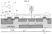
- the figure 4 illustrates the operation of the read circuit structure in the case where the first type is the type P, and the second type is the type N, as in the example of the figure 3 .
- the charge recovery structure that is to say the floating diffusion node 7
- RST the initialization signal
- the initialization transistor becomes on and the floating diffusion node 7 is then connected to the source of reference potential VDD, thus bringing it to an initial potential.
- This initial potential has a sufficient level to be able to make a total transfer of the charges collected by the buried collection diode 6 when an electrical channel connects the collection diode to the charge recovery structure.
- the initialization signal RST applied to the gate of the initialization transistor 10 is brought back to a low level, so that the initialization transistor becomes blocking again.
- the transfer signal TX applied to the gate of the transfer transistor 9 is brought to a high level, so as to allow the transfer of the accumulated charges in the second doped region 6 of the buried diode to the structure charge recovery device constituted by the floating diffusion node 7, by establishing an electrical channel in the substrate underlying the gate of the transfer transistor 9.
- the charges collected in the second doped region 6 of the collection diode are then transferred to the floating diffusion node 7 in full, so that the second doped region 6 is completely depleted at the end of this transfer.
- the depletion zone of the PN junction of the buried diode completely covers the second doped region 6.
- the potential at this level then corresponds to the so-called "pinning voltage" potential, which depends on the configuration of the dopants .
- the transfer signal TX applied to the gate of the transfer transistor 9 is brought to a low level so as to block the transfer transistor.
- a new cycle can then begin, whose instants t 0 ', t 1 ', t 2 'and t 3 ' respectively correspond to the instants t 0 , t 1 , t 2 and t 3 .
- a first reading of the signal via the output device 8 is made between times t 1 and t 2 , and a second reading is made after t 3 .
- the first reading informs about the reset level, that is to say the initial level of potential reached by the charge recovery structure after initialization.
- the integration time that is to say the collection of the charges injected by the buried collection diode 6, corresponds to the interval between the instants t 3 and t 3 ' .
- the voltage difference between the first reading and the second reading gives the desired image signal.
- the intervals between the instants t 0 and t 1 , as well as between the instants t 2 to t 3 are very short, of the order of a few nanoseconds to a few microseconds at the most, while the time between integration is of the order of a few milliseconds. It can therefore be seen that the charge transfer operation allows correlated double readings very close in time, since the first reading and the second reading take place respectively before and after the charge transfer, and are not separated by the time of the transfer. Integration as in the configurations of the state of the art previously exposed. The influence of noise 1 / f is reduced compared to these configurations.
- the figure 6 presents a reading circuit structure similar to that of the figure 3 , with however the presence of a confinement zone 13 formed by a doped region of the first type formed in the substrate 1, said confinement zone 13 extending in the depth of the substrate 1 at least opposite the first doped region 4 of the injection diode. As illustrated, the confinement zone 13 may further extend toward the surface of the substrate 1 to the periphery of the injection diode.
- This confinement zone 13 makes it possible to confine the charges injected by the injection diode into a region of the substrate 1 in which these charges are likely to be attracted by the buried diode.
- this confinement zone 13 corresponds to a deep P well ("P-Well" in English) which nevertheless leaves a region of the substrate 1 free between the injection diode and the buried diode.
- the figure 7 has another configuration, in which the charge recovery assembly 5 comprises a plurality of second doped regions 6 of the second type buried in the substrate 1 each forming a diode buried with said substrate, able to capture in the substrate at least a part charges injected by the common injection diode, and to accumulate these charges during a charge integration cycle.
- These buried diodes 6 in the substrate 1 are distributed around the injection diode 4, in different directions with respect to said injection diode.
- the injection diode 4 may be formed of a plurality of first doped regions of the second type electrically connected to each other.
- each of these first doped regions being situated close to at least one buried collection diode 6, that is to say at a distance less than the diffusion length of the electrons in the substrate 1 at a nominal temperature. use, for example at 20 ° C, and preferably less than 150 microns or 100 microns.
- the charge recovery assembly then comprises a plurality of charge recovery structures, for example floating diffusion nodes 7, each associated with a buried diode 6, and connected together to the same bus 8 to output the output signal.
- charge recovery structures for example floating diffusion nodes 7, each associated with a buried diode 6, and connected together to the same bus 8 to output the output signal.
- a transfer transistor makes it possible to control the transfer of charges from the buried diode to the charge recovery structure.
- the gates 10 of the transfer transistors are controlled by the same transfer signal TX.
- the figure 8 presents another possibility for the read circuit structure, which takes over the configuration of the figure 7 , in which the first type is the N type and the second type is the P type. It should be noted that the same modification can be made for the configurations exposed with reference to the figures 3 , 5 and 6 . Consequently, the substrate 1 here is of the N type, the first doped region 4 forming with the substrate the injection diode is of the P type, the second doped region 6 forming with the substrate the buried diode is of the P type, the structure recovery device has a P-doped region forming the floating diffusion node 7, and the confinement zone 13 is of the N-type.
- the charge carriers injected by the photodiode 2 outside the substrate 1 are holes, which are then collected by the buried diode and then recovered by the recovery structure.
- a second output device 19 is connected to the charge injection branch between the external charge source 2 and the injection diode 4.
- This second output device 19 comprises an amplifier 26a connected by a selection switch 27a to a multiplexing bus 28a, which may be distinct or confused with the multiplexing bus to which the output device 8 is connected.
- the input impedance of the amplifier 26a is very large, ideally infinite, equivalent to that of a MOS transistor gate.
- This second output device 19 allows a reading of the voltage across the injection diode and thus makes it possible to obtain a logarithmic reading of the current generated by the external charge source 2 and injected into the substrate 1, via the exponential relationship. between the voltage and the current flowing from the external charge source 2 to the injection diode. This gives the possibility of a dual reading mode: linear and logarithmic, which improves the dynamics of the read circuit structure since it can respond to both low and high light exposures.
- the figure 9 shows such an example, with a well-doped N-type well 14 formed in the P-type substrate 1, in which all of the doped regions mentioned above are formed.
Landscapes
- Engineering & Computer Science (AREA)
- Multimedia (AREA)
- Signal Processing (AREA)
- Solid State Image Pick-Up Elements (AREA)
- Transforming Light Signals Into Electric Signals (AREA)
Claims (15)
- Ausleseschaltungsstruktur, die auf einem Halbleitersubstrat (1) eines ersten Typs besteht und dazu bestimmt ist, die von einer Photodiode (2) außerhalb des Substrats (1) gemäß aufeinanderfolgenden Ladungsintegrationszyklen empfangenen Ladungen zu messen, wobei die Struktur umfasst:• an eine Injektionsdiode, die im Substrat (1) von einem ersten direkt polarisierten PN-Übergang gebildet wird, umfassend eine erste dotierte Region (4) eines zweiten Typs des Substrats (1), um elektrische Ladungen von der äußeren Photodiode (2) zu empfangen, und direkt polarisiert, um die von der äußeren Photodiode (2) empfangenen Ladungen in das Substrat (1) zu injizieren,• eine Sammeldiode, die im Substrat (1) von einem zweiten PN-Übergang gebildet wird, umfassend eine zweite dotierte Region (6) des zweiten Typs, die im Substrat (1) vergraben und dazu in der Lage ist, im Substrat (1) mindestens einen Teil der von der Injektionselektrode injizierten Ladungen zu sammeln und diese Ladungen während eines Integrationszyklus zu akkumulieren,• eine Ladungsrückgewinnungsstruktur (7, 15), die dafür konfiguriert ist, die in der Sammeldiode akkumulierten Ladungen rückzugewinnen,• Mittel, um die Ladungsrückgewinnungsstruktur (7, 15) am Ende jedes Integrationszyklus unter Zurücksetzen des elektrischen Potentials der Ladungsrückgewinnungsstruktur auf ein ursprüngliches Potential zu initialisieren,• wobei zwischen der ersten dotierten Region (4) und der zweiten dotierten Region (6) kein Transistor angeschlossen ist, wobei die erste Region (4) und die zweite Region durch Substrat (1) getrennt sind.
- Ausleseschaltungsstruktur nach Anspruch 1, wobei die Ladungsrückgewinnungsstruktur (7) einen schwebenden Diffusionsknoten (7) umfasst, der von einer dotierten Region des zweiten Typs im Substrat (1) gebildet wird, die mit einer Ausgangsvorrichtung (8) verbunden ist.
- Ausleseschaltungsstruktur nach dem vorstehenden Anspruch, wobei die Mittel, um die Ladungsrückgewinnungsstruktur zu initialisieren, einen Initialisierungstransistor (10) umfassen, dessen Gatter elektrisch vom Substrat (1) isoliert zwischen dem Diffusionsknoten (7) und einer Referenzpotentialquelle (VDD) liegt und dafür geeignet ist, angesteuert zu werden, um das Potential des Diffusionsknotens (7) auf das ursprüngliche Potential zu setzen.
- Ausleseschaltungsstruktur nach einem der Ansprüche 2 oder 3, umfassend einen Übertragungstransistor vom MOS-Typ, dessen Übertragungsgatter (9) zwischen der vergrabenen Diode und dem schwebenden Diffusionsknoten (7) liegt, oberhalb des Substrats (1) und elektrisch von demselben isoliert, und das angesteuert werden kann, um die in der zweiten dotierten Region (6) gesammelten Ladungen zum schwebenden Diffusionsknoten (7) zu übertragen.
- Ausleseschaltungsstruktur nach einem der vorstehenden Ansprüche, wobei die Ladungsrückgewinnungsstruktur umfasst• einen Speicher, der aus einer dotierten Region (15) des zweiten Typs besteht, und• einen schwebenden Diffusionsknoten (7), der von einer dotierten Region des zweiten Typs gebildet wird, welche mit einer Ausgangsvorrichtung (8) verbunden ist,wobei der Speicher im Substrat (1) zwischen der vergrabenen Elektrode und dem schwebenden Diffusionsknoten (7) gebildet ist.
- Ausleseschaltungsstruktur nach einem der vorstehenden Ansprüche, wobei zwischen die äußere Photodiode (2) und die Injektionsdiode eine Ausgangsvorrichtung (19) geschaltet ist, um ein Auslesen der Spannung an den Klemmen der Injektionsdiode zu ermöglichen und so eine logarithmische Auslesung des Stroms zu erhalten, der zwischen der äußeren Photodiode (2) und der Injektionsdiode fließt.
- Ausleseschaltungsstruktur nach einem der vorstehenden Ansprüche, umfassend eine Confinement-Zone (13), die von einer dotierten Region des ersten Typs gebildet wird, welche im Substrat (1) gebildet ist, wobei sich die Confinement-Zone (13) mindestens der ersten dotierten Region (4), aus welcher die Injektionsdiode besteht, zugewandt in die Tiefe des Substrats (1) erstreckt.
- Ausleseschaltungsstruktur nach dem vorstehenden Anspruch, wobei sich die Confinement-Zone (13) weiter bis zum Umfang der Injektionsdiode in Richtung der Oberfläche des Substrats (1) erstreckt.
- Ausleseschaltungsstruktur nach einem der vorstehenden Ansprüche, umfassend eine im Substrat (1) gebildete dotierte Region des ersten Typs (12), die eine dotierte Region des zweiten Typs (11) der Initialisierungsmittel umgibt, wobei die dotierte Region des zweiten Typs (11) mit einer Referenzpotentialquelle verbunden ist, und wobei sich die dotierte Region des ersten Typs bis zu einer dotierten Region des zweiten Typs erstreckt, die zur Ladungsrückgewinnungsstruktur (7) gehört.
- Ausleseschaltungsstruktur nach einem der vorstehenden Ansprüche, wobei die Ladungsrückgewinnungsanordnung eine Vielzahl von im Substrat (1) vergrabenen zweiten dotierten Regionen (6) des zweiten Typs umfasst, die jede zusammen mit dem Substrat (1) eine vergrabene Diode bilden, welche in der Lage ist, im Substrat mindestens einen Teil der Ladungen zu fangen, die von einer gemeinsamen Injektionsdiode (4) injiziert werden, und diese Ladungen während eines Ladungsintegrationszyklus zu akkumulieren.
- Ausleseschaltungsstruktur nach dem vorstehenden Anspruch, wobei die Injektionsdiode von einer Vielzahl erster dotierter Regionen des zweiten Typs gebildet wird, die elektrische miteinander verbunden sind.
- Ausleseschaltungsstruktur nach einem der vorstehenden Ansprüche, wobei die zweite dotierte Region (6) der vergrabenen Sammeldiode dafür konfiguriert ist, am Ende der Ladungsübertragung zur Ladungsrückgewinnungsstruktur (7) vollständig depletiert zu werden.
- Betriebsverfahren einer Ausleseschaltungsstruktur nach einem der vorstehenden Ansprüche, wobei- nach dem Initialisieren der Ladungsrückgewinnungsstruktur und vor dem Übertragen der Ladungen von der vergrabenen Diode zur Ladungsrückgewinnungsstruktur ein erstes Auslesen der Spannung im Bereich der Ladungsrückgewinnungsstruktur vorgenommen wird, und- nach dem Übertragen der Ladungen von der vergrabenen Diode zur Ladungsrückgewinnungsstruktur ein zweites Auslesen der Spannung im Bereich der Ladungsrückgewinnungsstruktur vorgenommen wird,wobei das Bildsignal der Differenz zwischen der ersten Auslesung und der zweiten Auslesung entspricht.
- Matrixförmige Ausleseschaltung, die eine Vielzahl von Ausleseschaltungsstrukturen nach einem der Ansprüche 1 bis 12 umfasst.
- Hybridsensor, umfassend ein erstes Substrat, auf dem eine Ausleseschaltung nach dem vorstehenden Anspruch gebildet ist, und ein zweites Substrat, auf dem eine Matrix aus für eine elektromagnetische Strahlung empfindlichen Elementen gebildet ist, aus denen die äußeren Photodioden (2) bestehen.
Applications Claiming Priority (2)
| Application Number | Priority Date | Filing Date | Title |
|---|---|---|---|
| FR1455361A FR3022425B1 (fr) | 2014-06-12 | 2014-06-12 | Structure de circuit de lecture a injection de charge |
| PCT/EP2015/063112 WO2015189359A1 (fr) | 2014-06-12 | 2015-06-12 | Structure de circuit de lecture a injection de charge |
Publications (2)
| Publication Number | Publication Date |
|---|---|
| EP3155662A1 EP3155662A1 (de) | 2017-04-19 |
| EP3155662B1 true EP3155662B1 (de) | 2019-10-23 |
Family
ID=51485686
Family Applications (1)
| Application Number | Title | Priority Date | Filing Date |
|---|---|---|---|
| EP15729435.6A Active EP3155662B1 (de) | 2014-06-12 | 2015-06-12 | Struktur einer ausleseschaltung mit ladungsinjektion |
Country Status (6)
| Country | Link |
|---|---|
| US (1) | US10332926B2 (de) |
| EP (1) | EP3155662B1 (de) |
| JP (1) | JP2017519375A (de) |
| CN (1) | CN106415842B (de) |
| FR (1) | FR3022425B1 (de) |
| WO (1) | WO2015189359A1 (de) |
Families Citing this family (5)
| Publication number | Priority date | Publication date | Assignee | Title |
|---|---|---|---|---|
| US11297258B2 (en) * | 2015-10-01 | 2022-04-05 | Qualcomm Incorporated | High dynamic range solid state image sensor and camera system |
| JP6705222B2 (ja) * | 2016-03-11 | 2020-06-03 | 富士通株式会社 | 画素駆動回路,イメージセンサおよび画素駆動回路のノイズ低減方法 |
| CN107658321B (zh) * | 2016-07-25 | 2019-12-27 | 南京威派视半导体技术有限公司 | 基于复合介质栅的双器件光敏探测单元、探测器及其方法 |
| FR3066344B1 (fr) * | 2017-05-10 | 2020-07-03 | New Imaging Technologies | Procede de correction des non-uniformites dans les capteurs d'image |
| FR3150902A1 (fr) * | 2023-07-06 | 2025-01-10 | Spectrum In Motion France | Structure d’interconnexion entre microcircuits |
Family Cites Families (8)
| Publication number | Priority date | Publication date | Assignee | Title |
|---|---|---|---|---|
| FR2656158B1 (fr) * | 1989-12-19 | 1992-02-28 | Thomson Composants Militaires | Photosenseur hybride. |
| US7786543B2 (en) * | 2002-08-27 | 2010-08-31 | E-Phocus | CDS capable sensor with photon sensing layer on active pixel circuit |
| KR100882979B1 (ko) * | 2007-09-07 | 2009-02-12 | 주식회사 동부하이텍 | 이미지센서 및 그 제조방법 |
| JP4835710B2 (ja) * | 2009-03-17 | 2011-12-14 | ソニー株式会社 | 固体撮像装置、固体撮像装置の製造方法、固体撮像装置の駆動方法、及び電子機器 |
| JP2012084644A (ja) * | 2010-10-08 | 2012-04-26 | Renesas Electronics Corp | 裏面照射型固体撮像装置 |
| FR2973162B1 (fr) * | 2011-03-23 | 2013-11-22 | E2V Semiconductors | Capteur d'image a tres haute dynamique |
| JP2013172210A (ja) * | 2012-02-17 | 2013-09-02 | Canon Inc | 撮像装置 |
| JP5959877B2 (ja) * | 2012-02-17 | 2016-08-02 | キヤノン株式会社 | 撮像装置 |
-
2014
- 2014-06-12 FR FR1455361A patent/FR3022425B1/fr not_active Expired - Fee Related
-
2015
- 2015-06-12 US US15/316,828 patent/US10332926B2/en active Active
- 2015-06-12 JP JP2017517412A patent/JP2017519375A/ja active Pending
- 2015-06-12 WO PCT/EP2015/063112 patent/WO2015189359A1/fr not_active Ceased
- 2015-06-12 EP EP15729435.6A patent/EP3155662B1/de active Active
- 2015-06-12 CN CN201580030693.1A patent/CN106415842B/zh not_active Expired - Fee Related
Non-Patent Citations (1)
| Title |
|---|
| None * |
Also Published As
| Publication number | Publication date |
|---|---|
| WO2015189359A1 (fr) | 2015-12-17 |
| CN106415842A (zh) | 2017-02-15 |
| FR3022425A1 (fr) | 2015-12-18 |
| US10332926B2 (en) | 2019-06-25 |
| JP2017519375A (ja) | 2017-07-13 |
| US20170213866A1 (en) | 2017-07-27 |
| EP3155662A1 (de) | 2017-04-19 |
| CN106415842B (zh) | 2019-06-14 |
| FR3022425B1 (fr) | 2017-09-01 |
Similar Documents
| Publication | Publication Date | Title |
|---|---|---|
| TWI541991B (zh) | 具有高度的短波長偵測效率之背側照明單光子崩潰二極體成像感測器系統 | |
| BE1023562B1 (fr) | Un dispositif detecteur assiste par un courant majoritaire. | |
| EP3155662B1 (de) | Struktur einer ausleseschaltung mit ladungsinjektion | |
| FR3046495A1 (fr) | Pixel de detection de temps de vol | |
| TW200818868A (en) | Method and apparatus providing dark current reduction in an active pixel sensor | |
| FR2930676A1 (fr) | Capteur d'image de tres faibles dimensions | |
| EP3016141A1 (de) | Bilderfassungssensor mit vertikalen elektroden | |
| EP2732473A1 (de) | Ingaas-lichtdiodenarray | |
| BE1022951B1 (fr) | Détecteur hybride à faible bruit utilisant le transfert de charge | |
| EP3155661B1 (de) | Verfahren zur bildaufnahme mit einem cmos-bildsensor | |
| FR2963163A1 (fr) | Procede de reinitialisation d'un photosite et photosite correspondant | |
| FR2924862A1 (fr) | Dispositif microelectronique photosensible avec multiplicateurs par avalanche | |
| FR3001578A1 (fr) | Matrice de photodiode a zone dopee absorbant les charges | |
| WO2010130950A1 (fr) | Capteur d'image integre a tres grande sensibilite | |
| EP4325573B1 (de) | Doppel-ctia für nicht-klemmbare photodiode | |
| WO2014060479A1 (fr) | Capteur d'image a efficacite quantique amelioree dans les grandes longueurs d'onde | |
| FR2945668A1 (fr) | Capteur d'image pour imagerie a tres bas niveau de lumiere. | |
| FR3152335A1 (fr) | Capteur d’images | |
| FR2682813A1 (fr) | Dispositif de visualisation de rayonnements infra-rouges. | |
| EP3000132A1 (de) | Fotodiodenarray mit einstellbarer ladungsabsorption | |
| Bogaerts et al. | Development of CMOS active pixel sensors for earth observation | |
| Saxena et al. | A Method of Estimating Indium Bump Integration Yield in Hybrid IRFPA of HgCdTe Photodiodes |
Legal Events
| Date | Code | Title | Description |
|---|---|---|---|
| STAA | Information on the status of an ep patent application or granted ep patent |
Free format text: STATUS: THE INTERNATIONAL PUBLICATION HAS BEEN MADE |
|
| PUAI | Public reference made under article 153(3) epc to a published international application that has entered the european phase |
Free format text: ORIGINAL CODE: 0009012 |
|
| STAA | Information on the status of an ep patent application or granted ep patent |
Free format text: STATUS: REQUEST FOR EXAMINATION WAS MADE |
|
| 17P | Request for examination filed |
Effective date: 20161214 |
|
| AK | Designated contracting states |
Kind code of ref document: A1 Designated state(s): AL AT BE BG CH CY CZ DE DK EE ES FI FR GB GR HR HU IE IS IT LI LT LU LV MC MK MT NL NO PL PT RO RS SE SI SK SM TR |
|
| AX | Request for extension of the european patent |
Extension state: BA ME |
|
| DAV | Request for validation of the european patent (deleted) | ||
| DAX | Request for extension of the european patent (deleted) | ||
| STAA | Information on the status of an ep patent application or granted ep patent |
Free format text: STATUS: EXAMINATION IS IN PROGRESS |
|
| 17Q | First examination report despatched |
Effective date: 20180726 |
|
| GRAP | Despatch of communication of intention to grant a patent |
Free format text: ORIGINAL CODE: EPIDOSNIGR1 |
|
| STAA | Information on the status of an ep patent application or granted ep patent |
Free format text: STATUS: GRANT OF PATENT IS INTENDED |
|
| INTG | Intention to grant announced |
Effective date: 20190701 |
|
| GRAS | Grant fee paid |
Free format text: ORIGINAL CODE: EPIDOSNIGR3 |
|
| GRAA | (expected) grant |
Free format text: ORIGINAL CODE: 0009210 |
|
| STAA | Information on the status of an ep patent application or granted ep patent |
Free format text: STATUS: THE PATENT HAS BEEN GRANTED |
|
| AK | Designated contracting states |
Kind code of ref document: B1 Designated state(s): AL AT BE BG CH CY CZ DE DK EE ES FI FR GB GR HR HU IE IS IT LI LT LU LV MC MK MT NL NO PL PT RO RS SE SI SK SM TR |
|
| REG | Reference to a national code |
Ref country code: GB Ref legal event code: FG4D Free format text: NOT ENGLISH |
|
| REG | Reference to a national code |
Ref country code: CH Ref legal event code: EP |
|
| REG | Reference to a national code |
Ref country code: IE Ref legal event code: FG4D Free format text: LANGUAGE OF EP DOCUMENT: FRENCH |
|
| REG | Reference to a national code |
Ref country code: DE Ref legal event code: R096 Ref document number: 602015040264 Country of ref document: DE |
|
| REG | Reference to a national code |
Ref country code: AT Ref legal event code: REF Ref document number: 1194662 Country of ref document: AT Kind code of ref document: T Effective date: 20191115 |
|
| REG | Reference to a national code |
Ref country code: NL Ref legal event code: MP Effective date: 20191023 |
|
| REG | Reference to a national code |
Ref country code: LT Ref legal event code: MG4D |
|
| PG25 | Lapsed in a contracting state [announced via postgrant information from national office to epo] |
Ref country code: BG Free format text: LAPSE BECAUSE OF FAILURE TO SUBMIT A TRANSLATION OF THE DESCRIPTION OR TO PAY THE FEE WITHIN THE PRESCRIBED TIME-LIMIT Effective date: 20200123 Ref country code: GR Free format text: LAPSE BECAUSE OF FAILURE TO SUBMIT A TRANSLATION OF THE DESCRIPTION OR TO PAY THE FEE WITHIN THE PRESCRIBED TIME-LIMIT Effective date: 20200124 Ref country code: NO Free format text: LAPSE BECAUSE OF FAILURE TO SUBMIT A TRANSLATION OF THE DESCRIPTION OR TO PAY THE FEE WITHIN THE PRESCRIBED TIME-LIMIT Effective date: 20200123 Ref country code: NL Free format text: LAPSE BECAUSE OF FAILURE TO SUBMIT A TRANSLATION OF THE DESCRIPTION OR TO PAY THE FEE WITHIN THE PRESCRIBED TIME-LIMIT Effective date: 20191023 Ref country code: PL Free format text: LAPSE BECAUSE OF FAILURE TO SUBMIT A TRANSLATION OF THE DESCRIPTION OR TO PAY THE FEE WITHIN THE PRESCRIBED TIME-LIMIT Effective date: 20191023 Ref country code: LT Free format text: LAPSE BECAUSE OF FAILURE TO SUBMIT A TRANSLATION OF THE DESCRIPTION OR TO PAY THE FEE WITHIN THE PRESCRIBED TIME-LIMIT Effective date: 20191023 Ref country code: LV Free format text: LAPSE BECAUSE OF FAILURE TO SUBMIT A TRANSLATION OF THE DESCRIPTION OR TO PAY THE FEE WITHIN THE PRESCRIBED TIME-LIMIT Effective date: 20191023 Ref country code: SE Free format text: LAPSE BECAUSE OF FAILURE TO SUBMIT A TRANSLATION OF THE DESCRIPTION OR TO PAY THE FEE WITHIN THE PRESCRIBED TIME-LIMIT Effective date: 20191023 Ref country code: FI Free format text: LAPSE BECAUSE OF FAILURE TO SUBMIT A TRANSLATION OF THE DESCRIPTION OR TO PAY THE FEE WITHIN THE PRESCRIBED TIME-LIMIT Effective date: 20191023 Ref country code: PT Free format text: LAPSE BECAUSE OF FAILURE TO SUBMIT A TRANSLATION OF THE DESCRIPTION OR TO PAY THE FEE WITHIN THE PRESCRIBED TIME-LIMIT Effective date: 20200224 |
|
| PG25 | Lapsed in a contracting state [announced via postgrant information from national office to epo] |
Ref country code: IS Free format text: LAPSE BECAUSE OF FAILURE TO SUBMIT A TRANSLATION OF THE DESCRIPTION OR TO PAY THE FEE WITHIN THE PRESCRIBED TIME-LIMIT Effective date: 20200224 Ref country code: RS Free format text: LAPSE BECAUSE OF FAILURE TO SUBMIT A TRANSLATION OF THE DESCRIPTION OR TO PAY THE FEE WITHIN THE PRESCRIBED TIME-LIMIT Effective date: 20191023 Ref country code: HR Free format text: LAPSE BECAUSE OF FAILURE TO SUBMIT A TRANSLATION OF THE DESCRIPTION OR TO PAY THE FEE WITHIN THE PRESCRIBED TIME-LIMIT Effective date: 20191023 |
|
| PG25 | Lapsed in a contracting state [announced via postgrant information from national office to epo] |
Ref country code: AL Free format text: LAPSE BECAUSE OF FAILURE TO SUBMIT A TRANSLATION OF THE DESCRIPTION OR TO PAY THE FEE WITHIN THE PRESCRIBED TIME-LIMIT Effective date: 20191023 |
|
| REG | Reference to a national code |
Ref country code: DE Ref legal event code: R097 Ref document number: 602015040264 Country of ref document: DE |
|
| PG2D | Information on lapse in contracting state deleted |
Ref country code: IS |
|
| PG25 | Lapsed in a contracting state [announced via postgrant information from national office to epo] |
Ref country code: ES Free format text: LAPSE BECAUSE OF FAILURE TO SUBMIT A TRANSLATION OF THE DESCRIPTION OR TO PAY THE FEE WITHIN THE PRESCRIBED TIME-LIMIT Effective date: 20191023 Ref country code: DK Free format text: LAPSE BECAUSE OF FAILURE TO SUBMIT A TRANSLATION OF THE DESCRIPTION OR TO PAY THE FEE WITHIN THE PRESCRIBED TIME-LIMIT Effective date: 20191023 Ref country code: EE Free format text: LAPSE BECAUSE OF FAILURE TO SUBMIT A TRANSLATION OF THE DESCRIPTION OR TO PAY THE FEE WITHIN THE PRESCRIBED TIME-LIMIT Effective date: 20191023 Ref country code: CZ Free format text: LAPSE BECAUSE OF FAILURE TO SUBMIT A TRANSLATION OF THE DESCRIPTION OR TO PAY THE FEE WITHIN THE PRESCRIBED TIME-LIMIT Effective date: 20191023 Ref country code: RO Free format text: LAPSE BECAUSE OF FAILURE TO SUBMIT A TRANSLATION OF THE DESCRIPTION OR TO PAY THE FEE WITHIN THE PRESCRIBED TIME-LIMIT Effective date: 20191023 Ref country code: IS Free format text: LAPSE BECAUSE OF FAILURE TO SUBMIT A TRANSLATION OF THE DESCRIPTION OR TO PAY THE FEE WITHIN THE PRESCRIBED TIME-LIMIT Effective date: 20200223 |
|
| REG | Reference to a national code |
Ref country code: AT Ref legal event code: MK05 Ref document number: 1194662 Country of ref document: AT Kind code of ref document: T Effective date: 20191023 |
|
| PLBE | No opposition filed within time limit |
Free format text: ORIGINAL CODE: 0009261 |
|
| STAA | Information on the status of an ep patent application or granted ep patent |
Free format text: STATUS: NO OPPOSITION FILED WITHIN TIME LIMIT |
|
| PG25 | Lapsed in a contracting state [announced via postgrant information from national office to epo] |
Ref country code: SK Free format text: LAPSE BECAUSE OF FAILURE TO SUBMIT A TRANSLATION OF THE DESCRIPTION OR TO PAY THE FEE WITHIN THE PRESCRIBED TIME-LIMIT Effective date: 20191023 Ref country code: IT Free format text: LAPSE BECAUSE OF FAILURE TO SUBMIT A TRANSLATION OF THE DESCRIPTION OR TO PAY THE FEE WITHIN THE PRESCRIBED TIME-LIMIT Effective date: 20191023 Ref country code: SM Free format text: LAPSE BECAUSE OF FAILURE TO SUBMIT A TRANSLATION OF THE DESCRIPTION OR TO PAY THE FEE WITHIN THE PRESCRIBED TIME-LIMIT Effective date: 20191023 |
|
| PGFP | Annual fee paid to national office [announced via postgrant information from national office to epo] |
Ref country code: GB Payment date: 20200619 Year of fee payment: 6 |
|
| 26N | No opposition filed |
Effective date: 20200724 |
|
| PG25 | Lapsed in a contracting state [announced via postgrant information from national office to epo] |
Ref country code: SI Free format text: LAPSE BECAUSE OF FAILURE TO SUBMIT A TRANSLATION OF THE DESCRIPTION OR TO PAY THE FEE WITHIN THE PRESCRIBED TIME-LIMIT Effective date: 20191023 Ref country code: AT Free format text: LAPSE BECAUSE OF FAILURE TO SUBMIT A TRANSLATION OF THE DESCRIPTION OR TO PAY THE FEE WITHIN THE PRESCRIBED TIME-LIMIT Effective date: 20191023 |
|
| PG25 | Lapsed in a contracting state [announced via postgrant information from national office to epo] |
Ref country code: MC Free format text: LAPSE BECAUSE OF FAILURE TO SUBMIT A TRANSLATION OF THE DESCRIPTION OR TO PAY THE FEE WITHIN THE PRESCRIBED TIME-LIMIT Effective date: 20191023 |
|
| REG | Reference to a national code |
Ref country code: CH Ref legal event code: PL |
|
| PG25 | Lapsed in a contracting state [announced via postgrant information from national office to epo] |
Ref country code: LU Free format text: LAPSE BECAUSE OF NON-PAYMENT OF DUE FEES Effective date: 20200612 |
|
| REG | Reference to a national code |
Ref country code: BE Ref legal event code: MM Effective date: 20200630 |
|
| PG25 | Lapsed in a contracting state [announced via postgrant information from national office to epo] |
Ref country code: LI Free format text: LAPSE BECAUSE OF NON-PAYMENT OF DUE FEES Effective date: 20200630 Ref country code: CH Free format text: LAPSE BECAUSE OF NON-PAYMENT OF DUE FEES Effective date: 20200630 Ref country code: IE Free format text: LAPSE BECAUSE OF NON-PAYMENT OF DUE FEES Effective date: 20200612 |
|
| PG25 | Lapsed in a contracting state [announced via postgrant information from national office to epo] |
Ref country code: BE Free format text: LAPSE BECAUSE OF NON-PAYMENT OF DUE FEES Effective date: 20200630 |
|
| GBPC | Gb: european patent ceased through non-payment of renewal fee |
Effective date: 20210612 |
|
| PG25 | Lapsed in a contracting state [announced via postgrant information from national office to epo] |
Ref country code: GB Free format text: LAPSE BECAUSE OF NON-PAYMENT OF DUE FEES Effective date: 20210612 |
|
| PG25 | Lapsed in a contracting state [announced via postgrant information from national office to epo] |
Ref country code: TR Free format text: LAPSE BECAUSE OF FAILURE TO SUBMIT A TRANSLATION OF THE DESCRIPTION OR TO PAY THE FEE WITHIN THE PRESCRIBED TIME-LIMIT Effective date: 20191023 Ref country code: MT Free format text: LAPSE BECAUSE OF FAILURE TO SUBMIT A TRANSLATION OF THE DESCRIPTION OR TO PAY THE FEE WITHIN THE PRESCRIBED TIME-LIMIT Effective date: 20191023 Ref country code: CY Free format text: LAPSE BECAUSE OF FAILURE TO SUBMIT A TRANSLATION OF THE DESCRIPTION OR TO PAY THE FEE WITHIN THE PRESCRIBED TIME-LIMIT Effective date: 20191023 |
|
| PG25 | Lapsed in a contracting state [announced via postgrant information from national office to epo] |
Ref country code: MK Free format text: LAPSE BECAUSE OF FAILURE TO SUBMIT A TRANSLATION OF THE DESCRIPTION OR TO PAY THE FEE WITHIN THE PRESCRIBED TIME-LIMIT Effective date: 20191023 |
|
| REG | Reference to a national code |
Ref country code: DE Ref legal event code: R079 Ref document number: 602015040264 Country of ref document: DE Free format text: PREVIOUS MAIN CLASS: H01L0027146000 Ipc: H10F0039180000 |
|
| PGFP | Annual fee paid to national office [announced via postgrant information from national office to epo] |
Ref country code: DE Payment date: 20250617 Year of fee payment: 11 |
|
| PGFP | Annual fee paid to national office [announced via postgrant information from national office to epo] |
Ref country code: FR Payment date: 20250513 Year of fee payment: 11 |