EP3155702B1 - Photoleitfähige dauerwellentetrahertzabbildungs- und -spektroskopiesysteme mit niedrigem tastverhältnis - Google Patents
Photoleitfähige dauerwellentetrahertzabbildungs- und -spektroskopiesysteme mit niedrigem tastverhältnis Download PDFInfo
- Publication number
- EP3155702B1 EP3155702B1 EP15807544.0A EP15807544A EP3155702B1 EP 3155702 B1 EP3155702 B1 EP 3155702B1 EP 15807544 A EP15807544 A EP 15807544A EP 3155702 B1 EP3155702 B1 EP 3155702B1
- Authority
- EP
- European Patent Office
- Prior art keywords
- photomixer
- optical pump
- frequency
- plasmonic
- radiation
- Prior art date
- Legal status (The legal status is an assumption and is not a legal conclusion. Google has not performed a legal analysis and makes no representation as to the accuracy of the status listed.)
- Not-in-force
Links
Images


Classifications
-
- G—PHYSICS
- G02—OPTICS
- G02F—OPTICAL DEVICES OR ARRANGEMENTS FOR THE CONTROL OF LIGHT BY MODIFICATION OF THE OPTICAL PROPERTIES OF THE MEDIA OF THE ELEMENTS INVOLVED THEREIN; NON-LINEAR OPTICS; FREQUENCY-CHANGING OF LIGHT; OPTICAL LOGIC ELEMENTS; OPTICAL ANALOGUE/DIGITAL CONVERTERS
- G02F1/00—Devices or arrangements for the control of the intensity, colour, phase, polarisation or direction of light arriving from an independent light source, e.g. switching, gating or modulating; Non-linear optics
- G02F1/35—Non-linear optics
- G02F1/353—Frequency conversion, i.e. wherein a light beam is generated with frequency components different from those of the incident light beams
- G02F1/3534—Three-wave interaction, e.g. sum-difference frequency generation
-
- G—PHYSICS
- G02—OPTICS
- G02F—OPTICAL DEVICES OR ARRANGEMENTS FOR THE CONTROL OF LIGHT BY MODIFICATION OF THE OPTICAL PROPERTIES OF THE MEDIA OF THE ELEMENTS INVOLVED THEREIN; NON-LINEAR OPTICS; FREQUENCY-CHANGING OF LIGHT; OPTICAL LOGIC ELEMENTS; OPTICAL ANALOGUE/DIGITAL CONVERTERS
- G02F2203/00—Function characteristic
- G02F2203/13—Function characteristic involving THZ radiation
Definitions
- the present invention generally relates to photomixing and more specifically to systems and methods for utilizing low-duty-cycles for various photomixers.
- Photomixing can involve pumping a high-speed photoconductor that is integrated with a radiating element with two frequency-offset pump lasers.
- the beams from the pump lasers are mixed together and focused onto a photomixer device (i.e. photoconductive source and/or detector) which generates the terahertz radiation.
- the frequency offset of the two pump lasers and, thus, the frequency of generated photocurrent and radiation can be set to a desired frequency.
- Technological breakthroughs in fiber optic communications and the availability of high power, widely tunable, narrow linewidth and compact fiber lasers and amplifiers have made telecommunication wavelengths a useful wavelength for pumping photomixers.
- a plasmonic photomixer with plasmonic contact electrode gratings allow efficient optical transmission through subwavelength metallic gratings into photo-absorbing active regions by excitation of surface plasmon waves (i.e. coherent electron oscillations that exist at the interface between two materials where the real part of the dielectric function changes sign across the interface) along the periodic metallic grating interface.
- surface plasmon waves i.e. coherent electron oscillations that exist at the interface between two materials where the real part of the dielectric function changes sign across the interface
- Various plasmonic photomixers can be utilized in accordance with embodiments of the invention including (but not limited to) those described in U.S. Patent Application No.
- the plasmonic photomixer utilizes the improved device quantum efficiency enabled by the enhanced photocarrier concentration near the plasmonic contact electrodes.
- the implementation and impact of plasmonic contact electrodes in enhancing the photomixer efficiency can be universally implemented and further utilized in a variety of photomixer architectures. In this regard, higher photomixer efficiencies can be achieved by using high aspect-ratio plasmonic contact electrodes and optical pump resonance cavities, as well as improved impedance matching and antenna performances.
- a plasmonic photomixer with plasmonic contact electrode gratings can be fabricated on any substrate that can absorb photons in an optical pump's operating wavelength ranges including (but not limited to) ErAs:InGaAs, ErAs compound, InGaAs compound, GaAs, InGaAs, Ge, InP, graphene, and GaN substrates.
- optical pumps can operate in the 700 to 1550nm wavelengths.
- the plasmonic photomixer offers an order of magnitude higher terahertz power levels compared to an analogous conventional photomixer having interdigitated contact electrodes in the 0.25-2.5 THz frequency range.
- photomixers in accordance with embodiments of the invention can utilize pump duty cycles below 50% to push the thermal breakdown onset to higher optical pump powers and achieve higher terahertz radiation powers.
- photoconductive terahertz sources and detectors in CW terahertz imaging and spectroscopy systems are pumped by a combination of two heterodyned CW optical pump beams with a terahertz frequency difference.
- the ultimate failure point of such devices is the thermal breakdown at high optical pump powers.
- higher radiation powers and detection sensitivities can be offered by photoconductive terahertz sources and detectors, respectively.
- Photomixing systems and methods in accordance with embodiments of the invention address the thermal breakdown limitations of photoconductive terahertz sources and detectors and can offer improved device performances.
- a low-duty-cycle optical pump is utilized where the terahertz imaging and spectroscopy systems operate in certain operation cycles followed by a sleep cycle, determined by the duty cycle of the optical pump.
- the terahertz source and detector are pumped and the generated and detected terahertz waves used to produce the output image and spectra of the terahertz imaging and spectroscopy system.
- the terahertz source and detector are not pumped, letting the device cool down while not producing any output data.
- the use of a low-duty-cycle optical pump can allow increasing the optical pump power at each operation cycle while maintaining a low average optical pump power. Therefore, high radiation powers and detection sensitivities can be achieved within each operation cycle without device failure due to thermal breakdown, and higher quality image and spectra data can be produced through the system.
- the plasmonic photomixer demonstrates up to 0.8 mW radiation power at 1 THz within each CW radiation cycle.
- the enhanced terahertz radiation powers offered by plasmonic photomixer in accordance with embodiments of the invention can be utilized for terahertz imaging and spectroscopy systems. Plasmonic photomixers in accordance with embodiments of the invention are further discussed below.
- Utilizing plasmonic nanostructures can be effective in enhancing the quantum efficiency of photoconductive terahertz optoelectronics.
- plasmonic nanostructures can be capable of manipulating the intensity of an incident optical pump beam and focusing it tightly next to the device contact electrodes.
- the number of the photocarriers drifted to the contact electrodes within a sub-picosecond timescale is increased and significantly higher quantum efficiency levels can be achieved.
- plasmonic nanostructures can enhance the optical-to-terahertz conversion efficiency of photomixers for continuous-wave, frequency-tunable terahertz generation.
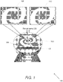
- FIG. 1 A schematic diagram of a plasmonic photomixer in comparison with an analogous photomixer based on a conventional design (i.e. having interdigitated contact electrodes) in accordance with an embodiment of the invention is illustrated in FIG. 1 .
- the plasmonic and conventional design can be implemented on a similar photomixer 106 fabricated on a ErAs:InGaAs substrate 102 with an integrated logarithmic spiral antennas 104 connected to an optical pump 116 to emit terahertz radiation 114 as further described below.
- the difference in the plasmonic and convention designs can be in the contact electrode designs as illustrated in 108 and 110, respectively.
- the plasmonic and conventional photomixers can be fabricated on a ErAs:InGaAs substrate 102 (carrier lifetime -0.85 ps) and integrated with identical logarithmic spiral antennas 104 as their terahertz radiating elements for comparison where the logarithmic spiral antennas are used to achieve the broadband radiation resistance and low antenna reactance values for terahertz generation with broad frequency tunability.
- various other antennas can also be utilized in accordance with embodiments of the invention, including (but not limited to) dipole, bow-tie, log-periodic, and folded dipole antennas.
- plasmonic photomixers in accordance with embodiments of the invention can utilize plasmonic contact electrode gratings covering a 4 ⁇ m ⁇ 8 ⁇ m area for both anode and cathode contact electrodes with an end-to-end spacing of 2 ⁇ m between the anode and cathode electrodes.
- many conventional photomixers typically utilize 0.2 ⁇ m wide interdigitated contact electrodes with a 1.8 ⁇ m gap between the electrodes.
- plasmonic contact electrodes can consist of metallic gratings with 200 nm pitch, 100 nm metal width, 5/45 nm Ti/Au height, and a 250 nm thick Si 3 N 4 anti-reflection coating. Typically, they are designed to allow coupling of more than ⁇ 70% of a transverse-magnetic (TM)-polarized optical pump in the 1550 nm wavelength range through the plasmonic contact electrodes into the ErAs:InGaAs substrate.
- TM transverse-magnetic
- the plasmonic contact electrodes and the interdigitated contact electrodes can be patterned using electron-beam lithography and formed by metal deposition and liftoff.
- the logarithmic spiral antennas and bias lines can be patterned using optical lithography and formed by metal deposition and liftoff. While specific plasmonic contact electrode designs are described above in regards to materials and grating specifications, various materials can be utilized including (but not limited to) gold, Ni, Pt, Ti and the geometry can vary depending on the substrate, metal type and wavelength such as (but not limited to) a pitch of 50nm - 2 ⁇ m, gap of 10nm - 700nm and thickness of 1nm. Although specific examples of utilizing plasmonic nanostructures for use with photomixers are discussed above with respect FIG.
- any of a variety of plasmonic nanostructures and their use with photomixers as appropriate to the requirements of a specific application can be utilized in accordance with embodiments of the invention.
- Experimental results characterizing plasmonic photomixers in accordance with embodiments of the invention are further discussed below.
- Plasmonic photomixers can be experimentally compared to conventional photomixers to highlight various characteristics of the plasmonic photomixers in accordance with embodiments of the invention.
- fabricated plasmonic and conventional (i.e. having interdigitated contact electrodes) photomixers can be mounted in the center of two hyper-hemispherical lenses and characterized under the same experimental conditions.
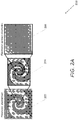
- Microscope and SEM images focusing on the contact electrodes of plasmonic and conventional photomixers fabricated on an ErAs:InGaAs substrate in accordance with an embodiment of the invention are illustrated in FIGS. 2A-B .
- the set of images 200 illustrate a fabricated plasmonic photomixer with a logarithmic spiral antenna integrated with plasmonic contact electrodes.
- the image 202 illustrates the plasmonic photomixer at a 200 ⁇ m resolution.
- the image 204 is a microscope image of the plasmonic photomixer at a 20 ⁇ m resolution.
- the image 206 is a SEM image that shows the plasmonic contact electrodes at a 2 ⁇ m resolution.
- the set of images 230 illustrate a fabricated conventional photomixer with a logarithmic spiral antenna integrated with interdigitated contact electrodes.
- the image 232 illustrates the conventional photomixer at a 200 ⁇ m resolution.
- the image 234 is a microscope image of the conventional photomixer at a 20 ⁇ m resolution.
- the image 236 is a SEM image that shows the interdigitated contact electrodes at a 2 ⁇ m resolution.
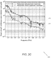
- the photomixers are pumped by two wavelength-tunable continuous-wave optical sources ( ⁇ ⁇ 1550 nm) with the same optical power, while controlling the radiation frequency by adjusting the frequency difference between the optical sources. Additionally, in order to mitigate thermal breakdown at high optical pump powers, the optical pump is modulated with a duty cycle less than 10% as further discussed below.
- FIG. 2C A graph illustrating radiated terahertz power from a plasmonic photomixer within each continuous-wave radiation cycle in comparison with an analogous conventional photomixer as a function of frequency in accordance with an embodiment of the invention is illustrated in FIG. 2C .
- the graph 270 illustrates the power at each continuous wave radiation cycle in microwatts for a photomixer with plasmonic electrodes 272 and a photomixer with interdigitated contact electrodes 274.
- a pump modulation frequency of 1 MHz, pump duty cycle of 2%, average pump power of 100 mW, and photomixer bias voltage of 3V was utilized.
- the results indicate an order of magnitude higher terahertz radiation power levels offered by the plasmonic photomixer over the 0.25-2.5 THz frequency range.
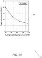
- a relative power enhancement factor can be defined as the ratio between the radiated power from the plasmonic photomixer and the conventional photomixer.
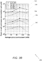
- a graph illustrating power enhancement factor as a function of average optical pump power in accordance with an embodiment of the invention is illustrated in FIG. 3A .
- the graph 300 illustrates that higher terahertz radiation enhancement factors are achieved at lower optical pump powers 302. This is because of the carrier screening effect that impacts the plasmonic photomixer more than the conventional photomixer at high optical pump powers. In the absence of the carrier screening effect at very low optical pump power levels, two orders of magnitude higher terahertz power levels are expected from the plasmonic photomixer.
- the radiated terahertz power within each continuous-wave radiation cycle can also be analyzed as a function of the average optical pump power, for a pump duty cycle of 2% and photomixer bias voltage of 3 V as illustrated in FIG. 3B .
- the graph 330 includes results for radiation at 0.25 THz 332, 0.5 THz 334, 1.0 THz 336, 1.5 THz 338, and 2.0 THz 340.
- the results indicate a quadratic increase in the radiated terahertz power within each radiation cycle as a function of the average pump power, which slightly degrades beyond 100 mW optical pump power due to the carrier screening effect.
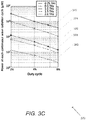
- the radiated terahertz power within each continuous-wave radiation cycle can also be analyzed in relation with the optical pump duty cycle, for an average optical pump power of 100 mW and photomixer bias voltage of 3 V as illustrated in FIG. 3C .
- the graph 330 includes results for radiation at 0.25 THz 372, 0.5 THz 374, 1.0 THz 376, 1.5 THz 378, and 2.0 THz 380.
- a pump modulation frequency of 1 MHz and pump duty cycles of 2%, 4%, 6%, and 8% are used, generating terahertz waves over 20, 40, 60, and 80 ns radiation cycles, respectively.
- reducing the optical pump duty cycle enables radiating higher terahertz power levels within each continuous-wave radiation cycle, while broadening the spectral linewidth of the radiated wave.
- a challenge toward developing high-performance photomixers operating at telecommunication pump wavelengths can be the high conductivity nature of photo-absorbing semiconductors in this wavelength range (e.g. InGaAs). This is because efficient acceleration of photocarriers inside high conductivity substrates may call for sufficient biasing accompanied by high dark current levels, which could lead to thermal breakdown especially at relatively high pump power levels.
- the optical pump can be modulated with a duty cycle below 50% in order to achieve high terahertz radiation power levels.
- the duty cycle is below 10%.
- the low-duty-cycle allows for increasing the optical pump power within each CW radiation cycle, while pushing the thermal breakdown onset to higher optical pump powers.
- at an average optical pump power of 150 mW with a pump modulation frequency of 1 MHz and pump duty cycle of 2% results demonstrate up to 0.8 mW radiation power at 1 THz, within each CW radiation cycle as further discussed below.
- FIG. 4A A microscope image of a plasmonic photomixer fabricated on an ErAs:InGaAs substrate, with a carrier lifetime of -0.85 ps, in accordance with an embodiment of the invention is illustrated in FIG. 4A .
- the set of images 400 illustrate the fabricated plasmonic photomixer with plasmonic contact electrodes.
- the image 402 illustrates the plasmonic photomixer at a 200 ⁇ m resolution.
- the image 404 is a microscope image of the plasmonic photomixer at a 20 ⁇ m resolution.
- the image 406 is a SEM image that shows the plasmonic contact electrodes at a 2 ⁇ m resolution.
- a logarithmic spiral antenna is used as the terahertz radiating element to achieve a broad radiation frequency range.
- the logarithmic spiral antenna can be designed to offer a broadband radiation resistance of 70-100 ⁇ while maintaining a reactance value near 0 ⁇ over the 0.1-2.5 THz frequency range.
- Each contact electrode of the plasmonic photomixer can be a plasmonic grating covering a 15x15 ⁇ m 2 area, with 200 nm pitch, 100 nm metal width, 5/45 nm Ti/Au height, and a 250 nm thick Si 3 N 4 anti-reflection coating.
- the plasmonic contact electrodes are designed to maximize device quantum efficiency at optical pump wavelength of 1550 nm.
- the end-to-end spacing between the anode and cathode contact electrodes is set to 10 ⁇ m to maintain the highest photocarrier drift velocity across the entire 15x15 ⁇ m 2 plasmonic contact electrode area.
- the fabrication process starts with patterning plasmonic contact electrode gratings using electron-beam lithography followed by deposition of Ti/Au (5/45 nm) and liftoff. A 250 nm Si 3 N 4 anti-reflection coating is then deposited using plasma-enhanced chemical vapor deposition. Next, contact vias can be patterned using optical lithography and formed using dry plasma etching. Finally, the logarithmic spiral antennas and bias lines can be patterned using optical lithography, followed by deposition of Ti/Au (10/400 nm) and liftoff.
- the fabricated plasmonic photomixers are then mounted on a hyper-hemispherical silicon lens and characterized using two frequency-offset pump lasers in the 1550 nm wavelength range.
- the optical pump is modulated with a duty cycle below 10%.
- Using short optical pump duty cycles allows increasing the optical pump power within each CW radiation cycle, while pushing the thermal breakdown onset to higher optical pump powers.
- the CW optical beam from the wavelength-tunable optical sources can be modulated at 1 MHz and then amplified using a pulsed fiber amplifier.
- the photomixers are characterized at 2%, 4%, 6%, and 8% pump duty cycles, generating terahertz waves over 20, 40, 60, and 80 ns CW radiation cycles, respectively.
- the experimental setup 500 can consist of two fiber-coupled CW lasers, one 502 with a fixed wavelength at 1545.4 nm (such as but not limited to QPhotonics QDFBLD-1550-10) and the other one 504 with a tunable wavelength (such as but not limited to Santec TSL-510) connected to polarization controllers 506.
- the output of the two lasers can be combined in a 2:1 fiber combiner 508 and modulated by an acousto-optic modulator 508 (such as but not limited to NEOS Technologies 15200-.2-1.55-LTD-GaP-FO).
- the pulsed laser beam is then amplified using a pulse amplifier 512 (such as but not limited to Optilab APEDFA-C-10) and focused onto the plasmonic photomixer 526 utilizing a grade index (GRIN) lens 514 and attenuator 516.
- a pulse amplifier 512 such as but not limited to Optilab APEDFA-C-10
- GRIN grade index
- the incident light from two laser sources should be linearly polarized with equal power levels.
- a quarter waveplate 518 can be used to convert the polarization of the laser light to circular polarization and convert it back to a linear polarization using a linear polarizer 520.
- a pellicle 522 can be used to separate a -8% of the laser beam to be monitored by an optical spectrum analyzer 524.
- the generated terahertz radiation can be measured via a silicon bolometer 528, while tuning the wavelength of the tunable laser.
- Plasmonic photomixers can be characterized and analyzed in consideration of pump duty cycles.
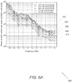
- the radiated terahertz power within each CW radiation cycle as a function of the average optical pump power, for a radiation duty cycle of 2% and photomixer bias voltage of 10 V is illustrated in FIG. 6A .
- the graph 600 illustrates results for optical pump powers of 150 mW 602, 125 mW 604, 100 mW 606, 75 mW 608, and 50 mW 610.
- the radiated terahertz power within each CW radiation cycle can increase quadratically as a function of the average pump power as illustrated in FIG. 6B .
- the graph 650 illustrates results for radiation of 0.25 THz 652, 0.5 THz 654, 1.0 THz 656, 1.5 THz 658, and 2.0 THz 660.
- terahertz radiation powers as high as 0.8 mW can be achieved at 1 THz over 20 ns CW radiation cycles, corresponding to a spectral linewidth broadening of 50 MHz.
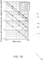
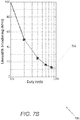
- the tradeoff between the radiated terahertz power and spectral linewidth as a function of the pump duty cycle is illustrated in FIG. 7A .
- the graph 700 illustrates results for radiation of 0.25 THz 702, 0.5 THz 704, 1.0 THz 706, 1.5 THz 708, and 2.0 THz 710.
- the terahertz power measurements are taken at an average optical pump power of 100 mW and a pump modulation frequency of 1 MHz.
- radiation power levels as high as 300 ⁇ W, 75 ⁇ W, 35 ⁇ W, and 20 ⁇ W are measured at 1 THz over 20, 40, 60, and 80 ns CW radiation cycles, corresponding to 50, 25, 16, and 12.5 MHz linewidth broadening, respectively as further illustrated in FIG. 7B .
- the radiation linewidth broadening is estimated using the Fourier theory.
- the graph 750 illustrates that the use of shorter optical pump duty cycles allows increasing the optical pump power within each CW radiation cycle, while pushing the thermal breakdown onset to higher optical pump powers 752.
- the terahertz radiation power from the photomixer has a quadratic relation with the optical pump power
- reducing the optical pump duty cycle dramatically increases the optical-to-terahertz conversion efficiency and the maximum radiated power from a photomixer before thermal breakdown.
- use of shorter CW radiation cycles results in broader radiation linewidths. Therefore, the duty cycle and repetition rate of the optical pump should be carefully selected to satisfy the spectral linewidth requirements of the specific application the photomixer is used for.
- reducing the pump modulation frequency in our measurements would reduce the radiation linewidth while offering the same terahertz radiation power levels at a given optical pump duty cycle.
Landscapes
- Physics & Mathematics (AREA)
- Nonlinear Science (AREA)
- General Physics & Mathematics (AREA)
- Optics & Photonics (AREA)
- Optical Modulation, Optical Deflection, Nonlinear Optics, Optical Demodulation, Optical Logic Elements (AREA)
Claims (13)
- Photomischsystem (100), das konfiguriert ist, Terahertz-Frequenzsignale im Dauerstrichbetrieb zu erzeugen, umfassend:eine optische Pumpe (116), die konfiguriert ist zum:Erzeugen von mindestens zwei Strahlen, wobei die mindestens zwei Strahlen dazu verwendet werden, einen Frequenzoffset zu erzeugen; undArbeiten mit einem Tastverhältnis unterhalb von 50%, wobei das Tastverhältnis einen Betriebszyklus und einen Schlafzyklus aufweist; undeinen Fotomischer (106), der ein Strahlungselement umfasst, das konfiguriert ist, den Frequenzoffset zu empfangen und unter Verwendung des empfangenen Frequenzoffsets und des Strahlungselements eine Terahertz-Strahlung (114) zu erzeugen, gekennzeichnet dadurch, dassdas Strahlungselement mindestens eine plasmonische Kontaktelektrode aufweist und dass die optische Pumpe mit einer durchschnittlichen optischen Pumpleistung von weniger als oder gleich 150 mW arbeitet.
- Photomischsystem (100) nach Anspruch 1, wobei das Strahlungselement eine Antenne ist, die für Breitbandstrahlung geeignet ist.
- Photomischsystem (100) nach Anspruch 2, wobei das Strahlungselement ausgewählt ist aus der Gruppe bestehend aus einer logarithmischen Spiralantenne (104), einer Dipolantenne, einer Schmetterlingsantenne, einer logarithmisch periodischen Antenne und einer gefalteten Dipolantenne.
- Photomischsystem (100) nach Anspruch 1, wobei der Photomischer (106) auf einem Substrat hergestellt ist, das dazu geeignet ist, Photonen im Betriebswellenlängenbereich der optischen Pumpe zu absorbieren.
- Photomischsystem (100) nach Anspruch 4, wobei der Photomischer (106) auf einem Substrat hergestellt ist, das ausgewählt ist aus der Gruppe bestehend aus ErAs:InGaAs (102), einer ErAs-Verbindung, einer InGaAs-Verbindung, GaAs, InGaAs, Ge, InP, Graphen, und GaN-Substraten.
- Photomischsystem (100) nach Anspruch 1, wobei die erzeugte Terahertz-Strahlung (114) einen Frequenzbereich von 0,25 bis 2,5 THz aufweist.
- Photomischsystem (100) nach Anspruch 1, wobei die erzeugte Terahertz-Strahlung (114) frequenzabstimmbar ist.
- Verfahren zur Erzeugung von Terahertz-Frequenzsignalen im Dauerstrichbetrieb unter Verwendung eines Photomischsystems (100) nach Anspruch 1, umfassend:Erzeugen von mindestens zwei Strahlen unter Verwendung einer optischen Pumpe (116), wobei die mindestens zwei Strahlen dazu verwendet werden, einen Frequenzoffset zu erzeugen;Betreiben der optischen Pumpe (116) mit einem Tastverhältnis unterhalb von 50%, wobei das Tastverhältnis einen Betriebszyklus und einen Schlafzyklus aufweist, wobei die optische Pumpe mit einer durchschnittlichen optischen Pumpleistung von weniger als oder gleich 150 mW arbeitet;Empfangen des Frequenzoffsets unter Verwendung eines Fotomischers (106), wobei der Fotomischer (106) ein Strahlungselement umfasst, wobei das Strahlungselement mindestens eine plasmonische Kontaktelektrode aufweist; undErzeugen einer Terahertz-Strahlung (114) basierend auf dem empfangenen Frequenzoffset und dem Strahlungselement.
- Verfahren nach Anspruch 8, wobei das Strahlungselement eine Antenne ist, die für Breitbandstrahlung geeignet ist.
- Verfahren nach Anspruch 8, wobei der Fotomischer (106) auf einem Substrat hergestellt ist, das dazu geeignet ist, Photonen im Betriebswellenlängenbereich der optischen Pumpe zu absorbieren.
- Verfahren des Systems nach Anspruch 10, wobei der Photomischer (106) auf einem Substrat hergestellt wird, das ausgewählt ist aus der Gruppe bestehend aus ErAs:InGaAs (102), einer ErAs-Verbindung, einer InGaAs-Verbindung, GaAs, InGaAs, Ge, InP, Graphen, und GaN-Substraten.
- Verfahren nach Anspruch 8, wobei die erzeugte Terahertz-Strahlung (114) einen Frequenzbereich von 0,25 bis 2,5 THz aufweist.
- Verfahren nach Anspruch 8, wobei die erzeugte Terahertz-Strahlung (114) frequenzabstimmbar ist.
Applications Claiming Priority (2)
| Application Number | Priority Date | Filing Date | Title |
|---|---|---|---|
| US201462011848P | 2014-06-13 | 2014-06-13 | |
| PCT/US2015/035685 WO2015192094A1 (en) | 2014-06-13 | 2015-06-12 | Low-duty-cycle continuous-wave photoconductive terahertz imaging and spectroscopy systems |
Publications (3)
| Publication Number | Publication Date |
|---|---|
| EP3155702A1 EP3155702A1 (de) | 2017-04-19 |
| EP3155702A4 EP3155702A4 (de) | 2018-07-18 |
| EP3155702B1 true EP3155702B1 (de) | 2020-12-16 |
Family
ID=54834465
Family Applications (1)
| Application Number | Title | Priority Date | Filing Date |
|---|---|---|---|
| EP15807544.0A Not-in-force EP3155702B1 (de) | 2014-06-13 | 2015-06-12 | Photoleitfähige dauerwellentetrahertzabbildungs- und -spektroskopiesysteme mit niedrigem tastverhältnis |
Country Status (4)
| Country | Link |
|---|---|
| US (1) | US10120263B2 (de) |
| EP (1) | EP3155702B1 (de) |
| JP (1) | JP6955337B2 (de) |
| WO (1) | WO2015192094A1 (de) |
Cited By (4)
| Publication number | Priority date | Publication date | Assignee | Title |
|---|---|---|---|---|
| US11112305B2 (en) | 2012-01-23 | 2021-09-07 | The Regents Of The University Of California | Photoconductive detector device with plasmonic electrodes |
| US11906424B2 (en) | 2019-10-01 | 2024-02-20 | The Regents Of The University Of California | Method for identifying chemical and structural variations through terahertz time-domain spectroscopy |
| US12066380B2 (en) | 2019-10-31 | 2024-08-20 | The Regents Of The University Of California | Methods and systems for detecting water status in plants using terahertz radiation |
| US12498615B2 (en) | 2020-12-01 | 2025-12-16 | The Regents Of The University Of California | Systems and methods for wavelength conversion through plasmon-coupled surface states |
Families Citing this family (9)
| Publication number | Priority date | Publication date | Assignee | Title |
|---|---|---|---|---|
| JP6955337B2 (ja) | 2014-06-13 | 2021-10-27 | ザ リージェンツ オブ ザ ユニバーシティ オブ カリフォルニアThe Regents Of The University Of California | 低デューティサイクル連続波光伝導性テラヘルツ撮像および分光システム |
| CN106159641B (zh) | 2016-09-05 | 2017-07-18 | 华讯方舟科技有限公司 | 携带轨道角动量的太赫兹波的发生装置及产生方法 |
| KR101885656B1 (ko) | 2016-10-25 | 2018-08-06 | 엘지전자 주식회사 | 차량용 램프 |
| EP3612812B1 (de) | 2017-04-20 | 2024-12-04 | The Regents of the University of California | Verfahren für hochfrequenznanoskopie |
| EP3775758A4 (de) | 2018-04-02 | 2021-10-27 | The Regents of the University of California | System und verfahren für photomixer-basiertes heterodynes hochfrequenzspektrometer und empfänger |
| US11262639B2 (en) * | 2020-04-03 | 2022-03-01 | Microtech Instruments, Inc. | Apparatus and methods for upconversion of a millimeter-wave signal and detection of the upconverted signal |
| KR102458236B1 (ko) * | 2021-08-25 | 2022-10-25 | 한국전자통신연구원 | 테라헤르츠 소자의 제조 방법 |
| CN114812803B (zh) * | 2022-03-31 | 2025-01-14 | 南京大学 | 一种平面等角螺旋天线结构的太赫兹探测器及其制备方法 |
| CN115876324A (zh) * | 2022-12-15 | 2023-03-31 | 北京无线电计量测试研究所 | 一种高分辨力太赫兹脉冲探测装置和方法 |
Family Cites Families (17)
| Publication number | Priority date | Publication date | Assignee | Title |
|---|---|---|---|---|
| WO2004034533A1 (en) | 2002-10-10 | 2004-04-22 | Teraview Limited | Terahertz quantum cascade laser |
| JP4749156B2 (ja) * | 2004-01-29 | 2011-08-17 | 潤一 西澤 | 電磁波発生装置 |
| JP4423429B2 (ja) * | 2004-09-13 | 2010-03-03 | 国立大学法人九州工業大学 | テラヘルツ電磁波放射素子及びその製造方法 |
| JP4609993B2 (ja) * | 2004-12-08 | 2011-01-12 | 独立行政法人理化学研究所 | テラヘルツ波発生方法及び装置 |
| DE102006014801A1 (de) * | 2006-03-29 | 2007-10-04 | Rwth Aachen University | THz-Antennen-Array, System und Verfahren zur Herstellung eines THz-Antennen-Arrays |
| US7515801B2 (en) * | 2006-12-28 | 2009-04-07 | Wisconsin Alumni Research Foundation | Coherent terahertz radiation source |
| US8492966B2 (en) | 2009-09-25 | 2013-07-23 | Mark J. Hagmann | Symmetric field emission devices using distributed capacitive ballasting with multiple emitters to obtain large emitted currents at high frequencies |
| KR101385108B1 (ko) * | 2009-12-17 | 2014-04-29 | 한국전자통신연구원 | 포토믹서 모듈 및 그것의 테라헤르츠파 발생 방법 |
| KR101145778B1 (ko) * | 2010-09-17 | 2012-05-16 | 한국전자통신연구원 | 주파수 가변형 테라헤르츠 송수신기들 및 듀얼 파장 레이저의 제작 방법 |
| US9935355B2 (en) * | 2010-10-29 | 2018-04-03 | Agency For Science, Technology And Research | THz photomixer emitter and method |
| KR101746508B1 (ko) * | 2010-12-13 | 2017-06-27 | 한국전자통신연구원 | 테라헤르츠파 발생기 |
| KR20120072214A (ko) * | 2010-12-23 | 2012-07-03 | 한국전자통신연구원 | 테라헤르츠 연속파 발생장치 |
| US8805148B2 (en) | 2011-07-14 | 2014-08-12 | International Business Machines Corporation | Generation of terahertz electromagnetic waves in graphene by coherent photon-mixing |
| KR20130073450A (ko) * | 2011-12-23 | 2013-07-03 | 한국전자통신연구원 | 테라헤르츠파 생성기 및 테라헤르츠파 생성 방법 |
| JP6169614B2 (ja) * | 2012-01-23 | 2017-07-26 | ザ・リージェンツ・オブ・ザ・ユニバーシティ・オブ・ミシガンThe Regents Of The University Of Michigan | プラズモン電極を有する光伝導装置 |
| JP6955337B2 (ja) | 2014-06-13 | 2021-10-27 | ザ リージェンツ オブ ザ ユニバーシティ オブ カリフォルニアThe Regents Of The University Of California | 低デューティサイクル連続波光伝導性テラヘルツ撮像および分光システム |
| US20160064110A1 (en) * | 2014-09-02 | 2016-03-03 | University Of Maryland | Plasmonic activated graphene terahertz generating devices and systems |
-
2015
- 2015-06-12 JP JP2016572427A patent/JP6955337B2/ja active Active
- 2015-06-12 US US15/318,347 patent/US10120263B2/en active Active
- 2015-06-12 WO PCT/US2015/035685 patent/WO2015192094A1/en not_active Ceased
- 2015-06-12 EP EP15807544.0A patent/EP3155702B1/de not_active Not-in-force
Non-Patent Citations (1)
| Title |
|---|
| None * |
Cited By (5)
| Publication number | Priority date | Publication date | Assignee | Title |
|---|---|---|---|---|
| US11112305B2 (en) | 2012-01-23 | 2021-09-07 | The Regents Of The University Of California | Photoconductive detector device with plasmonic electrodes |
| US11231318B2 (en) | 2012-01-23 | 2022-01-25 | The Regents Of The University Of California | Photoconductive detector device with plasmonic electrodes |
| US11906424B2 (en) | 2019-10-01 | 2024-02-20 | The Regents Of The University Of California | Method for identifying chemical and structural variations through terahertz time-domain spectroscopy |
| US12066380B2 (en) | 2019-10-31 | 2024-08-20 | The Regents Of The University Of California | Methods and systems for detecting water status in plants using terahertz radiation |
| US12498615B2 (en) | 2020-12-01 | 2025-12-16 | The Regents Of The University Of California | Systems and methods for wavelength conversion through plasmon-coupled surface states |
Also Published As
| Publication number | Publication date |
|---|---|
| WO2015192094A1 (en) | 2015-12-17 |
| US10120263B2 (en) | 2018-11-06 |
| JP2017523601A (ja) | 2017-08-17 |
| EP3155702A1 (de) | 2017-04-19 |
| US20170123292A1 (en) | 2017-05-04 |
| JP6955337B2 (ja) | 2021-10-27 |
| EP3155702A4 (de) | 2018-07-18 |
Similar Documents
| Publication | Publication Date | Title |
|---|---|---|
| EP3155702B1 (de) | Photoleitfähige dauerwellentetrahertzabbildungs- und -spektroskopiesysteme mit niedrigem tastverhältnis | |
| US11231318B2 (en) | Photoconductive detector device with plasmonic electrodes | |
| Tani et al. | Generation of terahertz radiation by photomixing with dual-and multiple-mode lasers | |
| Yardimci et al. | Nanostructure‐enhanced photoconductive terahertz emission and detection | |
| Yardimci et al. | High power telecommunication-compatible photoconductive terahertz emitters based on plasmonic nano-antenna arrays | |
| Berry et al. | Significant performance enhancement in photoconductive terahertz optoelectronics by incorporating plasmonic contact electrodes | |
| Berry et al. | High power terahertz generation using 1550 nm plasmonic photomixers | |
| Lepeshov et al. | Enhancement of terahertz photoconductive antenna operation by optical nanoantennas | |
| Yardimci et al. | High-power terahertz generation using large-area plasmonic photoconductive emitters | |
| Tani et al. | Generation of coherent terahertz radiation by photomixing of dual-mode lasers | |
| Tanoto et al. | Greatly enhanced continuous-wave terahertz emission by nano-electrodes in a photoconductive photomixer | |
| Yang et al. | Tunable terahertz wave generation through a bimodal laser diode and plasmonic photomixer | |
| Lu et al. | Bias-free terahertz generation from a silicon-compatible photoconductive emitter operating at telecommunication wavelengths | |
| US12140477B2 (en) | System and method for photomixer-based heterodyne high-frequency spectrometer and receiver | |
| CN118190154A (zh) | 宽频谱太赫兹外差探测器 | |
| Yang et al. | High-power continuous-wave terahertz generation through plasmonic photomixers | |
| Wang et al. | Broadband heterodyne terahertz detector based on plasmonic photomixing | |
| Yang et al. | A high-power photomixer with plasmonic contact electrodes | |
| Lu et al. | Plasmonics‐enhanced photoconductive terahertz devices | |
| Turan et al. | Telecommunication-Compatible Bias-Free Photoconductive Source with a 5 THz Radiation Bandwidth | |
| Yardimci et al. | 1550 nm Large-area plasmonic photoconductive terahertz sources | |
| Yang et al. | High-performance continuous-wave terahertz emitters based on plasmonic photomixing antennas | |
| Yardimci et al. | Plasmonic nano-antenna arrays for high-sensitivity and broadband terahertz detection | |
| Turan et al. | 25 mW Pulsed Terahertz Radiation from Bias-Free, Telecommunication-Compatible Plasmonic Nanoantennas | |
| Yang et al. | Spectral characterization of high-power plasmonic photomixers |
Legal Events
| Date | Code | Title | Description |
|---|---|---|---|
| STAA | Information on the status of an ep patent application or granted ep patent |
Free format text: STATUS: THE INTERNATIONAL PUBLICATION HAS BEEN MADE |
|
| PUAI | Public reference made under article 153(3) epc to a published international application that has entered the european phase |
Free format text: ORIGINAL CODE: 0009012 |
|
| STAA | Information on the status of an ep patent application or granted ep patent |
Free format text: STATUS: REQUEST FOR EXAMINATION WAS MADE |
|
| 17P | Request for examination filed |
Effective date: 20161122 |
|
| AK | Designated contracting states |
Kind code of ref document: A1 Designated state(s): AL AT BE BG CH CY CZ DE DK EE ES FI FR GB GR HR HU IE IS IT LI LT LU LV MC MK MT NL NO PL PT RO RS SE SI SK SM TR |
|
| AX | Request for extension of the european patent |
Extension state: BA ME |
|
| DAV | Request for validation of the european patent (deleted) | ||
| DAX | Request for extension of the european patent (deleted) | ||
| A4 | Supplementary search report drawn up and despatched |
Effective date: 20180620 |
|
| RIC1 | Information provided on ipc code assigned before grant |
Ipc: H01S 3/091 20060101AFI20180614BHEP Ipc: G02F 1/35 20060101ALI20180614BHEP |
|
| GRAP | Despatch of communication of intention to grant a patent |
Free format text: ORIGINAL CODE: EPIDOSNIGR1 |
|
| STAA | Information on the status of an ep patent application or granted ep patent |
Free format text: STATUS: GRANT OF PATENT IS INTENDED |
|
| INTG | Intention to grant announced |
Effective date: 20200826 |
|
| GRAS | Grant fee paid |
Free format text: ORIGINAL CODE: EPIDOSNIGR3 |
|
| GRAA | (expected) grant |
Free format text: ORIGINAL CODE: 0009210 |
|
| STAA | Information on the status of an ep patent application or granted ep patent |
Free format text: STATUS: THE PATENT HAS BEEN GRANTED |
|
| AK | Designated contracting states |
Kind code of ref document: B1 Designated state(s): AL AT BE BG CH CY CZ DE DK EE ES FI FR GB GR HR HU IE IS IT LI LT LU LV MC MK MT NL NO PL PT RO RS SE SI SK SM TR |
|
| REG | Reference to a national code |
Ref country code: GB Ref legal event code: FG4D |
|
| REG | Reference to a national code |
Ref country code: IE Ref legal event code: FG4D |
|
| REG | Reference to a national code |
Ref country code: DE Ref legal event code: R096 Ref document number: 602015063623 Country of ref document: DE |
|
| REG | Reference to a national code |
Ref country code: AT Ref legal event code: REF Ref document number: 1346459 Country of ref document: AT Kind code of ref document: T Effective date: 20210115 |
|
| PG25 | Lapsed in a contracting state [announced via postgrant information from national office to epo] |
Ref country code: GR Free format text: LAPSE BECAUSE OF FAILURE TO SUBMIT A TRANSLATION OF THE DESCRIPTION OR TO PAY THE FEE WITHIN THE PRESCRIBED TIME-LIMIT Effective date: 20210317 Ref country code: RS Free format text: LAPSE BECAUSE OF FAILURE TO SUBMIT A TRANSLATION OF THE DESCRIPTION OR TO PAY THE FEE WITHIN THE PRESCRIBED TIME-LIMIT Effective date: 20201216 Ref country code: FI Free format text: LAPSE BECAUSE OF FAILURE TO SUBMIT A TRANSLATION OF THE DESCRIPTION OR TO PAY THE FEE WITHIN THE PRESCRIBED TIME-LIMIT Effective date: 20201216 Ref country code: NO Free format text: LAPSE BECAUSE OF FAILURE TO SUBMIT A TRANSLATION OF THE DESCRIPTION OR TO PAY THE FEE WITHIN THE PRESCRIBED TIME-LIMIT Effective date: 20210316 |
|
| REG | Reference to a national code |
Ref country code: AT Ref legal event code: MK05 Ref document number: 1346459 Country of ref document: AT Kind code of ref document: T Effective date: 20201216 |
|
| REG | Reference to a national code |
Ref country code: NL Ref legal event code: MP Effective date: 20201216 |
|
| PG25 | Lapsed in a contracting state [announced via postgrant information from national office to epo] |
Ref country code: LV Free format text: LAPSE BECAUSE OF FAILURE TO SUBMIT A TRANSLATION OF THE DESCRIPTION OR TO PAY THE FEE WITHIN THE PRESCRIBED TIME-LIMIT Effective date: 20201216 Ref country code: SE Free format text: LAPSE BECAUSE OF FAILURE TO SUBMIT A TRANSLATION OF THE DESCRIPTION OR TO PAY THE FEE WITHIN THE PRESCRIBED TIME-LIMIT Effective date: 20201216 Ref country code: BG Free format text: LAPSE BECAUSE OF FAILURE TO SUBMIT A TRANSLATION OF THE DESCRIPTION OR TO PAY THE FEE WITHIN THE PRESCRIBED TIME-LIMIT Effective date: 20210316 |
|
| PG25 | Lapsed in a contracting state [announced via postgrant information from national office to epo] |
Ref country code: NL Free format text: LAPSE BECAUSE OF FAILURE TO SUBMIT A TRANSLATION OF THE DESCRIPTION OR TO PAY THE FEE WITHIN THE PRESCRIBED TIME-LIMIT Effective date: 20201216 Ref country code: HR Free format text: LAPSE BECAUSE OF FAILURE TO SUBMIT A TRANSLATION OF THE DESCRIPTION OR TO PAY THE FEE WITHIN THE PRESCRIBED TIME-LIMIT Effective date: 20201216 |
|
| REG | Reference to a national code |
Ref country code: LT Ref legal event code: MG9D |
|
| PG25 | Lapsed in a contracting state [announced via postgrant information from national office to epo] |
Ref country code: SK Free format text: LAPSE BECAUSE OF FAILURE TO SUBMIT A TRANSLATION OF THE DESCRIPTION OR TO PAY THE FEE WITHIN THE PRESCRIBED TIME-LIMIT Effective date: 20201216 Ref country code: RO Free format text: LAPSE BECAUSE OF FAILURE TO SUBMIT A TRANSLATION OF THE DESCRIPTION OR TO PAY THE FEE WITHIN THE PRESCRIBED TIME-LIMIT Effective date: 20201216 Ref country code: PT Free format text: LAPSE BECAUSE OF FAILURE TO SUBMIT A TRANSLATION OF THE DESCRIPTION OR TO PAY THE FEE WITHIN THE PRESCRIBED TIME-LIMIT Effective date: 20210416 Ref country code: LT Free format text: LAPSE BECAUSE OF FAILURE TO SUBMIT A TRANSLATION OF THE DESCRIPTION OR TO PAY THE FEE WITHIN THE PRESCRIBED TIME-LIMIT Effective date: 20201216 Ref country code: CZ Free format text: LAPSE BECAUSE OF FAILURE TO SUBMIT A TRANSLATION OF THE DESCRIPTION OR TO PAY THE FEE WITHIN THE PRESCRIBED TIME-LIMIT Effective date: 20201216 Ref country code: EE Free format text: LAPSE BECAUSE OF FAILURE TO SUBMIT A TRANSLATION OF THE DESCRIPTION OR TO PAY THE FEE WITHIN THE PRESCRIBED TIME-LIMIT Effective date: 20201216 Ref country code: SM Free format text: LAPSE BECAUSE OF FAILURE TO SUBMIT A TRANSLATION OF THE DESCRIPTION OR TO PAY THE FEE WITHIN THE PRESCRIBED TIME-LIMIT Effective date: 20201216 |
|
| PG25 | Lapsed in a contracting state [announced via postgrant information from national office to epo] |
Ref country code: AT Free format text: LAPSE BECAUSE OF FAILURE TO SUBMIT A TRANSLATION OF THE DESCRIPTION OR TO PAY THE FEE WITHIN THE PRESCRIBED TIME-LIMIT Effective date: 20201216 Ref country code: PL Free format text: LAPSE BECAUSE OF FAILURE TO SUBMIT A TRANSLATION OF THE DESCRIPTION OR TO PAY THE FEE WITHIN THE PRESCRIBED TIME-LIMIT Effective date: 20201216 |
|
| REG | Reference to a national code |
Ref country code: DE Ref legal event code: R097 Ref document number: 602015063623 Country of ref document: DE |
|
| PG25 | Lapsed in a contracting state [announced via postgrant information from national office to epo] |
Ref country code: IS Free format text: LAPSE BECAUSE OF FAILURE TO SUBMIT A TRANSLATION OF THE DESCRIPTION OR TO PAY THE FEE WITHIN THE PRESCRIBED TIME-LIMIT Effective date: 20210416 |
|
| PLBE | No opposition filed within time limit |
Free format text: ORIGINAL CODE: 0009261 |
|
| STAA | Information on the status of an ep patent application or granted ep patent |
Free format text: STATUS: NO OPPOSITION FILED WITHIN TIME LIMIT |
|
| PG25 | Lapsed in a contracting state [announced via postgrant information from national office to epo] |
Ref country code: IT Free format text: LAPSE BECAUSE OF FAILURE TO SUBMIT A TRANSLATION OF THE DESCRIPTION OR TO PAY THE FEE WITHIN THE PRESCRIBED TIME-LIMIT Effective date: 20201216 Ref country code: AL Free format text: LAPSE BECAUSE OF FAILURE TO SUBMIT A TRANSLATION OF THE DESCRIPTION OR TO PAY THE FEE WITHIN THE PRESCRIBED TIME-LIMIT Effective date: 20201216 |
|
| 26N | No opposition filed |
Effective date: 20210917 |
|
| PG25 | Lapsed in a contracting state [announced via postgrant information from national office to epo] |
Ref country code: DK Free format text: LAPSE BECAUSE OF FAILURE TO SUBMIT A TRANSLATION OF THE DESCRIPTION OR TO PAY THE FEE WITHIN THE PRESCRIBED TIME-LIMIT Effective date: 20201216 Ref country code: ES Free format text: LAPSE BECAUSE OF FAILURE TO SUBMIT A TRANSLATION OF THE DESCRIPTION OR TO PAY THE FEE WITHIN THE PRESCRIBED TIME-LIMIT Effective date: 20201216 |
|
| PG25 | Lapsed in a contracting state [announced via postgrant information from national office to epo] |
Ref country code: MC Free format text: LAPSE BECAUSE OF FAILURE TO SUBMIT A TRANSLATION OF THE DESCRIPTION OR TO PAY THE FEE WITHIN THE PRESCRIBED TIME-LIMIT Effective date: 20201216 |
|
| REG | Reference to a national code |
Ref country code: CH Ref legal event code: PL |
|
| PG25 | Lapsed in a contracting state [announced via postgrant information from national office to epo] |
Ref country code: SI Free format text: LAPSE BECAUSE OF FAILURE TO SUBMIT A TRANSLATION OF THE DESCRIPTION OR TO PAY THE FEE WITHIN THE PRESCRIBED TIME-LIMIT Effective date: 20201216 |
|
| REG | Reference to a national code |
Ref country code: BE Ref legal event code: MM Effective date: 20210630 |
|
| PG25 | Lapsed in a contracting state [announced via postgrant information from national office to epo] |
Ref country code: LU Free format text: LAPSE BECAUSE OF NON-PAYMENT OF DUE FEES Effective date: 20210612 |
|
| PG25 | Lapsed in a contracting state [announced via postgrant information from national office to epo] |
Ref country code: LI Free format text: LAPSE BECAUSE OF NON-PAYMENT OF DUE FEES Effective date: 20210630 Ref country code: IE Free format text: LAPSE BECAUSE OF NON-PAYMENT OF DUE FEES Effective date: 20210612 Ref country code: CH Free format text: LAPSE BECAUSE OF NON-PAYMENT OF DUE FEES Effective date: 20210630 |
|
| PG25 | Lapsed in a contracting state [announced via postgrant information from national office to epo] |
Ref country code: IS Free format text: LAPSE BECAUSE OF FAILURE TO SUBMIT A TRANSLATION OF THE DESCRIPTION OR TO PAY THE FEE WITHIN THE PRESCRIBED TIME-LIMIT Effective date: 20210416 |
|
| PG25 | Lapsed in a contracting state [announced via postgrant information from national office to epo] |
Ref country code: BE Free format text: LAPSE BECAUSE OF NON-PAYMENT OF DUE FEES Effective date: 20210630 |
|
| PG25 | Lapsed in a contracting state [announced via postgrant information from national office to epo] |
Ref country code: HU Free format text: LAPSE BECAUSE OF FAILURE TO SUBMIT A TRANSLATION OF THE DESCRIPTION OR TO PAY THE FEE WITHIN THE PRESCRIBED TIME-LIMIT; INVALID AB INITIO Effective date: 20150612 |
|
| PG25 | Lapsed in a contracting state [announced via postgrant information from national office to epo] |
Ref country code: CY Free format text: LAPSE BECAUSE OF FAILURE TO SUBMIT A TRANSLATION OF THE DESCRIPTION OR TO PAY THE FEE WITHIN THE PRESCRIBED TIME-LIMIT Effective date: 20201216 |
|
| P01 | Opt-out of the competence of the unified patent court (upc) registered |
Effective date: 20230528 |
|
| PGFP | Annual fee paid to national office [announced via postgrant information from national office to epo] |
Ref country code: DE Payment date: 20230626 Year of fee payment: 9 |
|
| PG25 | Lapsed in a contracting state [announced via postgrant information from national office to epo] |
Ref country code: MK Free format text: LAPSE BECAUSE OF FAILURE TO SUBMIT A TRANSLATION OF THE DESCRIPTION OR TO PAY THE FEE WITHIN THE PRESCRIBED TIME-LIMIT Effective date: 20201216 |
|
| PG25 | Lapsed in a contracting state [announced via postgrant information from national office to epo] |
Ref country code: TR Free format text: LAPSE BECAUSE OF FAILURE TO SUBMIT A TRANSLATION OF THE DESCRIPTION OR TO PAY THE FEE WITHIN THE PRESCRIBED TIME-LIMIT Effective date: 20201216 |
|
| PGFP | Annual fee paid to national office [announced via postgrant information from national office to epo] |
Ref country code: GB Payment date: 20240627 Year of fee payment: 10 |
|
| PGFP | Annual fee paid to national office [announced via postgrant information from national office to epo] |
Ref country code: FR Payment date: 20240625 Year of fee payment: 10 |
|
| PG25 | Lapsed in a contracting state [announced via postgrant information from national office to epo] |
Ref country code: MT Free format text: LAPSE BECAUSE OF FAILURE TO SUBMIT A TRANSLATION OF THE DESCRIPTION OR TO PAY THE FEE WITHIN THE PRESCRIBED TIME-LIMIT Effective date: 20201216 |
|
| REG | Reference to a national code |
Ref country code: DE Ref legal event code: R119 Ref document number: 602015063623 Country of ref document: DE |
|
| GBPC | Gb: european patent ceased through non-payment of renewal fee |
Effective date: 20250612 |
|
| PG25 | Lapsed in a contracting state [announced via postgrant information from national office to epo] |
Ref country code: GB Free format text: LAPSE BECAUSE OF NON-PAYMENT OF DUE FEES Effective date: 20250612 |
|
| PG25 | Lapsed in a contracting state [announced via postgrant information from national office to epo] |
Ref country code: DE Free format text: LAPSE BECAUSE OF NON-PAYMENT OF DUE FEES Effective date: 20260101 |
|
| PG25 | Lapsed in a contracting state [announced via postgrant information from national office to epo] |
Ref country code: FR Free format text: LAPSE BECAUSE OF NON-PAYMENT OF DUE FEES Effective date: 20250630 |