EP3156991A1 - Élément optique de dispositif d'affichage à del et dispositif d'affichage à del - Google Patents
Élément optique de dispositif d'affichage à del et dispositif d'affichage à del Download PDFInfo
- Publication number
- EP3156991A1 EP3156991A1 EP16188050.5A EP16188050A EP3156991A1 EP 3156991 A1 EP3156991 A1 EP 3156991A1 EP 16188050 A EP16188050 A EP 16188050A EP 3156991 A1 EP3156991 A1 EP 3156991A1
- Authority
- EP
- European Patent Office
- Prior art keywords
- led
- unit lenses
- width
- display apparatus
- unit
- Prior art date
- Legal status (The legal status is an assumption and is not a legal conclusion. Google has not performed a legal analysis and makes no representation as to the accuracy of the status listed.)
- Granted
Links
Images




Classifications
-
- G—PHYSICS
- G09—EDUCATION; CRYPTOGRAPHY; DISPLAY; ADVERTISING; SEALS
- G09F—DISPLAYING; ADVERTISING; SIGNS; LABELS OR NAME-PLATES; SEALS
- G09F9/00—Indicating arrangements for variable information in which the information is built-up on a support by selection or combination of individual elements
- G09F9/30—Indicating arrangements for variable information in which the information is built-up on a support by selection or combination of individual elements in which the desired character or characters are formed by combining individual elements
- G09F9/302—Indicating arrangements for variable information in which the information is built-up on a support by selection or combination of individual elements in which the desired character or characters are formed by combining individual elements characterised by the form or geometrical disposition of the individual elements
- G09F9/3026—Video wall, i.e. stackable semiconductor matrix display modules
-
- G—PHYSICS
- G02—OPTICS
- G02B—OPTICAL ELEMENTS, SYSTEMS OR APPARATUS
- G02B3/00—Simple or compound lenses
- G02B3/0006—Arrays
- G02B3/0037—Arrays characterized by the distribution or form of lenses
- G02B3/0056—Arrays characterized by the distribution or form of lenses arranged along two different directions in a plane, e.g. honeycomb arrangement of lenses
-
- H—ELECTRICITY
- H05—ELECTRIC TECHNIQUES NOT OTHERWISE PROVIDED FOR
- H05B—ELECTRIC HEATING; ELECTRIC LIGHT SOURCES NOT OTHERWISE PROVIDED FOR; CIRCUIT ARRANGEMENTS FOR ELECTRIC LIGHT SOURCES, IN GENERAL
- H05B33/00—Electroluminescent light sources
- H05B33/12—Light sources with substantially two-dimensional [2D] radiating surfaces
- H05B33/14—Light sources with substantially two-dimensional [2D] radiating surfaces characterised by the chemical or physical composition or the arrangement of the electroluminescent material, or by the simultaneous addition of the electroluminescent material in or onto the light source
- H05B33/145—Arrangements of the electroluminescent material
-
- F—MECHANICAL ENGINEERING; LIGHTING; HEATING; WEAPONS; BLASTING
- F21—LIGHTING
- F21K—NON-ELECTRIC LIGHT SOURCES USING LUMINESCENCE; LIGHT SOURCES USING ELECTROCHEMILUMINESCENCE; LIGHT SOURCES USING CHARGES OF COMBUSTIBLE MATERIAL; LIGHT SOURCES USING SEMICONDUCTOR DEVICES AS LIGHT-GENERATING ELEMENTS; LIGHT SOURCES NOT OTHERWISE PROVIDED FOR
- F21K9/00—Light sources using semiconductor devices as light-generating elements, e.g. using light-emitting diodes [LED] or lasers
- F21K9/20—Light sources comprising attachment means
-
- F—MECHANICAL ENGINEERING; LIGHTING; HEATING; WEAPONS; BLASTING
- F21—LIGHTING
- F21K—NON-ELECTRIC LIGHT SOURCES USING LUMINESCENCE; LIGHT SOURCES USING ELECTROCHEMILUMINESCENCE; LIGHT SOURCES USING CHARGES OF COMBUSTIBLE MATERIAL; LIGHT SOURCES USING SEMICONDUCTOR DEVICES AS LIGHT-GENERATING ELEMENTS; LIGHT SOURCES NOT OTHERWISE PROVIDED FOR
- F21K9/00—Light sources using semiconductor devices as light-generating elements, e.g. using light-emitting diodes [LED] or lasers
- F21K9/60—Optical arrangements integrated in the light source, e.g. for improving the colour rendering index or the light extraction
- F21K9/65—Optical arrangements integrated in the light source, e.g. for improving the colour rendering index or the light extraction specially adapted for changing the characteristics or the distribution of the light, e.g. by adjustment of parts
-
- F—MECHANICAL ENGINEERING; LIGHTING; HEATING; WEAPONS; BLASTING
- F21—LIGHTING
- F21S—NON-PORTABLE LIGHTING DEVICES; SYSTEMS THEREOF; VEHICLE LIGHTING DEVICES SPECIALLY ADAPTED FOR VEHICLE EXTERIORS
- F21S2/00—Systems of lighting devices, not provided for in main groups F21S4/00 - F21S10/00 or F21S19/00, e.g. of modular construction
- F21S2/005—Systems of lighting devices, not provided for in main groups F21S4/00 - F21S10/00 or F21S19/00, e.g. of modular construction of modular construction
-
- F—MECHANICAL ENGINEERING; LIGHTING; HEATING; WEAPONS; BLASTING
- F21—LIGHTING
- F21V—FUNCTIONAL FEATURES OR DETAILS OF LIGHTING DEVICES OR SYSTEMS THEREOF; STRUCTURAL COMBINATIONS OF LIGHTING DEVICES WITH OTHER ARTICLES, NOT OTHERWISE PROVIDED FOR
- F21V23/00—Arrangement of electric circuit elements in or on lighting devices
- F21V23/003—Arrangement of electric circuit elements in or on lighting devices the elements being electronics drivers or controllers for operating the light source, e.g. for a LED array
-
- F—MECHANICAL ENGINEERING; LIGHTING; HEATING; WEAPONS; BLASTING
- F21—LIGHTING
- F21V—FUNCTIONAL FEATURES OR DETAILS OF LIGHTING DEVICES OR SYSTEMS THEREOF; STRUCTURAL COMBINATIONS OF LIGHTING DEVICES WITH OTHER ARTICLES, NOT OTHERWISE PROVIDED FOR
- F21V5/00—Refractors for light sources
- F21V5/007—Array of lenses or refractors for a cluster of light sources, e.g. for arrangement of multiple light sources in one plane
-
- F—MECHANICAL ENGINEERING; LIGHTING; HEATING; WEAPONS; BLASTING
- F21—LIGHTING
- F21V—FUNCTIONAL FEATURES OR DETAILS OF LIGHTING DEVICES OR SYSTEMS THEREOF; STRUCTURAL COMBINATIONS OF LIGHTING DEVICES WITH OTHER ARTICLES, NOT OTHERWISE PROVIDED FOR
- F21V5/00—Refractors for light sources
- F21V5/02—Refractors for light sources of prismatic shape
-
- F—MECHANICAL ENGINEERING; LIGHTING; HEATING; WEAPONS; BLASTING
- F21—LIGHTING
- F21V—FUNCTIONAL FEATURES OR DETAILS OF LIGHTING DEVICES OR SYSTEMS THEREOF; STRUCTURAL COMBINATIONS OF LIGHTING DEVICES WITH OTHER ARTICLES, NOT OTHERWISE PROVIDED FOR
- F21V5/00—Refractors for light sources
- F21V5/04—Refractors for light sources of lens shape
-
- G—PHYSICS
- G09—EDUCATION; CRYPTOGRAPHY; DISPLAY; ADVERTISING; SEALS
- G09F—DISPLAYING; ADVERTISING; SIGNS; LABELS OR NAME-PLATES; SEALS
- G09F13/00—Illuminated signs; Luminous advertising
- G09F13/20—Illuminated signs; Luminous advertising with luminescent surfaces or parts
- G09F13/22—Illuminated signs; Luminous advertising with luminescent surfaces or parts electroluminescent
-
- G—PHYSICS
- G09—EDUCATION; CRYPTOGRAPHY; DISPLAY; ADVERTISING; SEALS
- G09F—DISPLAYING; ADVERTISING; SIGNS; LABELS OR NAME-PLATES; SEALS
- G09F19/00—Advertising or display means not otherwise provided for
- G09F19/12—Advertising or display means not otherwise provided for using special optical effects
-
- G—PHYSICS
- G09—EDUCATION; CRYPTOGRAPHY; DISPLAY; ADVERTISING; SEALS
- G09F—DISPLAYING; ADVERTISING; SIGNS; LABELS OR NAME-PLATES; SEALS
- G09F9/00—Indicating arrangements for variable information in which the information is built-up on a support by selection or combination of individual elements
- G09F9/30—Indicating arrangements for variable information in which the information is built-up on a support by selection or combination of individual elements in which the desired character or characters are formed by combining individual elements
- G09F9/33—Indicating arrangements for variable information in which the information is built-up on a support by selection or combination of individual elements in which the desired character or characters are formed by combining individual elements being semiconductor devices, e.g. diodes
-
- H—ELECTRICITY
- H10—SEMICONDUCTOR DEVICES; ELECTRIC SOLID-STATE DEVICES NOT OTHERWISE PROVIDED FOR
- H10H—INORGANIC LIGHT-EMITTING SEMICONDUCTOR DEVICES HAVING POTENTIAL BARRIERS
- H10H20/00—Individual inorganic light-emitting semiconductor devices having potential barriers, e.g. light-emitting diodes [LED]
- H10H20/80—Constructional details
- H10H20/85—Packages
- H10H20/855—Optical field-shaping means, e.g. lenses
-
- H—ELECTRICITY
- H10—SEMICONDUCTOR DEVICES; ELECTRIC SOLID-STATE DEVICES NOT OTHERWISE PROVIDED FOR
- H10H—INORGANIC LIGHT-EMITTING SEMICONDUCTOR DEVICES HAVING POTENTIAL BARRIERS
- H10H20/00—Individual inorganic light-emitting semiconductor devices having potential barriers, e.g. light-emitting diodes [LED]
- H10H20/80—Constructional details
- H10H20/85—Packages
- H10H20/857—Interconnections, e.g. lead-frames, bond wires or solder balls
-
- H—ELECTRICITY
- H10—SEMICONDUCTOR DEVICES; ELECTRIC SOLID-STATE DEVICES NOT OTHERWISE PROVIDED FOR
- H10W—GENERIC PACKAGES, INTERCONNECTIONS, CONNECTORS OR OTHER CONSTRUCTIONAL DETAILS OF DEVICES COVERED BY CLASS H10
- H10W90/00—Package configurations
-
- F—MECHANICAL ENGINEERING; LIGHTING; HEATING; WEAPONS; BLASTING
- F21—LIGHTING
- F21Y—INDEXING SCHEME ASSOCIATED WITH SUBCLASSES F21K, F21L, F21S and F21V, RELATING TO THE FORM OR THE KIND OF THE LIGHT SOURCES OR OF THE COLOUR OF THE LIGHT EMITTED
- F21Y2113/00—Combination of light sources
- F21Y2113/10—Combination of light sources of different colours
- F21Y2113/13—Combination of light sources of different colours comprising an assembly of point-like light sources
-
- F—MECHANICAL ENGINEERING; LIGHTING; HEATING; WEAPONS; BLASTING
- F21—LIGHTING
- F21Y—INDEXING SCHEME ASSOCIATED WITH SUBCLASSES F21K, F21L, F21S and F21V, RELATING TO THE FORM OR THE KIND OF THE LIGHT SOURCES OR OF THE COLOUR OF THE LIGHT EMITTED
- F21Y2115/00—Light-generating elements of semiconductor light sources
- F21Y2115/10—Light-emitting diodes [LED]
-
- G—PHYSICS
- G09—EDUCATION; CRYPTOGRAPHY; DISPLAY; ADVERTISING; SEALS
- G09F—DISPLAYING; ADVERTISING; SIGNS; LABELS OR NAME-PLATES; SEALS
- G09F13/00—Illuminated signs; Luminous advertising
- G09F13/20—Illuminated signs; Luminous advertising with luminescent surfaces or parts
- G09F13/22—Illuminated signs; Luminous advertising with luminescent surfaces or parts electroluminescent
- G09F2013/222—Illuminated signs; Luminous advertising with luminescent surfaces or parts electroluminescent with LEDs
Definitions
- Apparatuses and methods consistent with exemplary embodiments relate to a light emitting diode (LED) display apparatus, and more specifically, to an optical element of an LED display apparatus capable of reducing Moire phenomenon and/or a blur phenomenon.
- LED light emitting diode
- An LED display apparatus has excellent brightness and color attributes, compared to other types of display apparatuses, e.g., an LCD display. As a result, an LED display apparatus is widely used in an indoor/outdoor billboard, an indoor/outdoor guide board, an electric sign of a sports stadium or an indoor/outdoor backdrop.
- a light emitting diode may be disposed in a matrix form of M*N (where M and N are natural numbers).
- a pitch between light emitting diodes arranged in a matrix form of an LED display apparatus is wider than other types of display apparatuses.
- an LED display apparatus having a non-light emitting region for example, a region between light emitting diodes
- unwanted pattern e.g., wave pattern or Moire pattern
- a blur phenomenon may also occur.
- a light emitting diode (LED) display apparatus including: an LED module including a plurality of LEDs mounted on a circuit board; and an optical film including a plurality of unit lenses configured to cover the LED module and transmit light emitted from the plurality of LEDs, wherein at least one of the plurality of unit lenses has a cross-lenticular lens shape or a cross-prismatic lens shape.
- LED light emitting diode
- Each of the plurality of LEDs may form one sub-pixel, and a plurality of sub-pixels may form one pixel of a screen of the LED display apparatus.
- the one pixel may be formed using a red LED, a green LED, and a blue LED.
- a cross-sectional shape of the plurality of unit lenses may include at least one of a triangle, a round, a triangle having round corners, and a polygonal having round corners.
- At least two unit lenses from among the plurality of unit lenses may have a different size of a cross-sectional shape.
- Multiple unit lenses may overlap one sub-pixel.
- a number of the unit lenses overlapping one sub-pixel may be equal to or greater than five.
- a width of a unit lens may be in a range of 20 ⁇ m to 50 ⁇ m.
- a raw material of the optical film may include at least one of acryl, polyethylene, polyethylene terephthalate (PET), resin, and silicone.
- the optical film may be bonded to the LED module using an adhesive.
- the optical film may further include a diffusing agent having a spherical shape.
- the diffusing agent may have a porous surface.
- a diameter of the diffusing agent may be smaller than a width of a unit lens of the optical film.
- the apparatus may further include: an LED panel including a plurality of the LED modules arranged in a matrix form; and an LED cabinet configured to support the LED panel and transfer at least one of power and a driving signal to the LED panel.
- a light emitting diode (LED) display apparatus including: a plurality of LED modules, each of which including a plurality of LEDs mounted on a circuit board in a matrix form; an LED panel on which the plurality of LED modules are arranged in a matrix form; and an optical film including a plurality of unit lenses configured to cover the plurality of LED modules and transmit light emitted from the plurality of LEDs, wherein at least one of the plurality of unit lenses has a cross-lenticular lens shape.
- At least one of the plurality of unit lenses may have a cross-prismatic lens shape.
- the apparatus may further include an LED cabinet configured to support the LED panel and transfer at least one of power and a driving signal to the plurality of LED modules.
- At least one of the power and the driving signal may be provided from an external source to the LED display apparatus.
- an optical element of an LED display apparatus may have a two-dimensional cross-lenticular lens shape to adjust light-transmissibility and/or light-diffusibility, thereby improving luminance, brightness, and/or a fill factor.
- an optical element of an LED display apparatus may have a two-dimensional cross-prismatic lens shape to adjust light-transmissibility and/or light-diffusibility, thereby improving luminance, brightness, and/or a fill factor.
- Terms including an ordinal number, such as “first,” “second,” etc. may be used to explain various components, and the above-mentioned components are not limited to the above-mentioned terms.
- the above-mentioned terms may be used for the purpose of distinguishing one component from another.
- a first component may be called a second component within the scope of rights of the present disclosure.
- the second component may be called the first component.
- the term “and/or” may include a combination of a plurality of recited items that are related to each other or any one of a plurality of recited items that are related to each other. Further, “film,” “sheet” or “plate” only differ in names, and may not be distinguished from one another.
- Content may be displayed in a display apparatus.
- Content may be received in a control apparatus and/or a display apparatus.
- content may include a video file reproduced in a video player, which is one of applications, or an audio file, a music file reproduced in a music player, a photo file displayed in a photo gallery, a webpage file displayed in a web browser, a text file, or etc.
- content may include broadcast being received.
- FIG. 1 is a schematic view illustrating an LED display apparatus, according to an exemplary embodiment.
- FIG. 1 shows that an LED display apparatus 100 is installed outdoors, but it would be readily understood by one of ordinary skill in the art that the LED display apparatus may be installed indoors according to another exemplary embodiment.
- the LED display apparatus 100 may be implemented as a billboard at a store, which displays merchants and/or price to provide information to customers.
- the LED display apparatus 100 may include LEDs respectively emitting a red light, a green light and/or a blue light in a matrix form. Further, referring to FIG. 5A , the LED display apparatus 100 may package a red LED 11 r, a green LED 11 g and a blue LED 11 b to form one pixel, and arrange them in a matrix form. Each of the LEDs, i.e., a red LED 11r, a green LED 11g and a blue LED 11b may be called a sub-pixel. Further, the LED display apparatus 100 may include an LED to emit a white color light and a color filter to extract various colors from the white color light.
- the LED display apparatus 100 may include a screen formed by a plurality of LEDs.
- the LED display apparatus 100 may display content by driving a plurality of LEDs.
- the LED display apparatus may provide a user with a good visibility due to its high brightness (for example, 2,500 nit). Further, the LED display apparatus 100 may have a waterproof and/or vibration-proof feature. The waterproof and/or vibration-proof feature may be determined with reference to an Ingress Protection rating.
- the LED display apparatus 100 may be fixed to a wall by a wall mount unit or by a stand, depending on a distance between provided information (for example, advertisement) and the user and/or an eye level of the user.
- provided information for example, advertisement
- the LED display apparatus 100 may include a plurality of LEDs 11 (see FIG. 2A ), a plurality of LED modules 10 (see FIG. 2A ) which display content using the plurality of LEDs 11, and/or an LED cabinet 120 (see FIG. 2B ) which supports the plurality of LED modules 10.
- the LED cabinet 120 may transfer power and/or a driving signal to the LED modules 10 and/or the LEDs 11.
- One LED module 10 or a plurality of LED modules 10 may be referred to as an LED panel 110.
- LED display apparatus 100 including 2*3 LED modules 10 is illustrated in FIG. 2A , it will be easily understood by one of ordinary skill in the art that the number and dispositional pattern of the LED modules 10 may be modified in various ways.
- the LED display apparatus 100 and components of the LED display apparatus 100 will be described in greater detail below.
- the LED display apparatus 100 may be implemented as a curved LED display apparatus having various curvatures.
- the LED display apparatus 100 may have a screen having a fixed (or one) curvature (e.g., 2500R), a plurality of curvatures (e.g., A first curvature of 2500R and a second curvature of 3000R).
- the LED display apparatus 100 may also be a curvature variable type LED display apparatus in which a curvature of a current screen changes according to a user input.
- examples of the LED display apparatus 100 are not limited thereto.
- An external control device may be connected to one side of the LED display apparatus 100.
- the LED display apparatus 100 may be connected to the control device through a communicator wirelessly.
- control device and the LED display apparatus 100 are connected to each other via cable and are respectively fixed to a wall by a wall mount unit, the control device may be positioned on the rear side of the LED display apparatus 100.
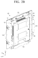
- FIGS. 2A and 2B illustrate respectively a front perspective view and a rear perspective view of an LED display apparatus according to an exemplary embodiment.
- the LED display apparatus 100 may include a plurality of LEDs 11, an LED module 10 including a circuit board 12 on which the plurality of LEDs 11 are mounted in a matrix form, an LED panel 110 including one or more LED modules, and an LED cabinet 120 which supports one or more LED panels 110.
- the LED 11 may be implemented using a red LED 11r, a green LED 11g, and a blue LED 11 b.
- each of the red LED 11r, the green LED 11g, and the blue LED 11b may be referred to as a sub-pixel.
- the red LED 11 r, the green LED 11g and the blue LED 11b, i.e., the sub-pixels may form a single pixel and may be arranged repetitively.
- the red LED 11r i.e., a sub-pixel, may be arranged along a line in the direction of gravity.
- the green LED 11 g i.e., a sub-pixel
- the blue LED 11 b i.e., a sub-pixel
- the green LED 11g may be arranged on the right side of the red LED 11r along a line in the direction of gravity.
- the plurality of LEDs 11 may be mounted on the circuit board 12 in a matrix form (for example, M*N, in which M and N are natural numbers).
- the size of arrays in the matrix may be the same (e.g., 16*16, 24*24, 32*32, or 64*64 array) or different from each other.
- the shape the circuit board 12 may vary according to exemplary embodiments. Examples of the shape of the circuit board 12 may include, but are not limited to, a triangle, a rectangle, and a polygon. To correspond to the circuit board 12, the LED module 10 may be triangular, quadrilateral or polygonal.
- a pitch between a plurality of LEDs 11 of the LED module 10 may be arranged in various ways to correspond to a resolution and/or size of the LED display apparatus 100.
- a red LED, a green LED and a blue LED may implement one pixel.
- the LED 11 may be driven (e.g., turned on, turned off, or flickered) by a driving signal transmitted from a timing controller 185.
- the LED panel 110 may be a group of the LED modules 10-1 to 10-6 arranged in a matrix form.
- the LED panel 110 may be triangular, quadrilateral (e.g., rectangle or square) or polygonal depending on the shape of one LED module 10 or the shape of a plurality of LED modules 10 arranged in a matrix form.
- a rear surface (e.g., opposite direction to light emission of LED) of the LED panel (or LED module) may be supported to intersect a direction of gravity (for example, -z direction) or may be supported in the direction of gravity by a front bracket 121 of the LED cabinet 120.
- the rear surface of the LED panel (or LED module) may be supported by a coupling member (e.g., bolt, rivet or magnet) of the front bracket 121 of the LED cabinet 120.
- the LED cabinet 120 may include the front bracket 121, a frame bracket 122, and a cover 123.
- the LED cabinet 120 may include a link bracket 124. Further, the LED cabinet 120 may include a handle 125.
- the front bracket 121 may support an LED panel (or LED module) and have an opening 121a (see FIG. 3 ). Through the opening 121a, a driving signal and/or power may be delivered to the LED panel (and/or LED module).
- An area of a base plate 121 may be larger than or equal to that of one or more LED modules 10. Further, if the LED display apparatus 100 is implemented as one LED panel 110, an area of the base plate 121 may be larger than or equal to that of the one LED panel 110.
- the frame bracket 122 may hold some of components of the LED display apparatus 100 in a rear surface (e.g., -y axis direction) of the front bracket 121.
- the frame bracket 122 may hold one of the timing controller 185 which provides a driving signal that controls the LED 11 and a power supply unit 190 which supplies power to the LED panel 110 or both. Further, the frame bracket 122 may hold a main board which controls the timing controller 185 and the power supply unit 190.
- the timing controller 185 may transmit a control signal for driving LED to the LED 11 according to a video (or image) received from the control device 100.
- the timing controller 185 may be connected to an external control device through an opening of the frame bracket 122 via cable.
- the cover 123 may open or close a rear surface of the frame bracket 122.
- the link bracket 124 may connect the LED cabinet 120 with another LED cabinet (e.g., 110-1 to 110-4) (see FIG. 6A ) positioned on one side (for example, upper, lower, left or right) of the LED cabinet 120 with a coupling member (e.g., bolt, rivet, or etc.).
- a coupling member e.g., bolt, rivet, or etc.
- the handle 125 may be used to move the LED cabinet 120.
- the LED display apparatus 100 may include a plurality of LED panels 110 disposed in a matrix form and a plurality of LED cabinets 120 corresponding to the plurality of LED panels 110.
- the number of the LED panels 110 and the LED cabinets 120 may vary according to exemplary embodiments.
- the LED display apparatus 100 may include one LED panel 110 and one LED cabinet 120.
- FIG. 3 illustrates a exploded perspective view of an LED display apparatus, according to an exemplary embodiment.
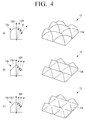
- FIG. 4 illustrates a cross-sectional view and a perspective view of an optical element of an LED display apparatus according to an exemplary embodiment.
- an optical element 13 may be bonded with an LED module (e.g., 10-6) including LED 11 and a circuit board 12 to prevent a Moire phenomenon.
- the optical element 13 may transmit light emitted from the LED. Further, the optical element 13 may change a proceeding direction of light emitted from the LED (e.g., by refraction or reflection).
- the optical element 13 may, for example, include a cross-lenticular lens film or a cross-prismatic lens film.
- the optical element 13 may, for example, include a cross-lenticular lens and/or a cross-prismatic lens.
- a user may view content displayed through an LED module (or LED panel) through the optical element 13.
- the term "optical element" may be interchangeable with "optical film.”
- the optical element 13 may be a cross-lenticular lens film or a cross-prismatic lens film having a lens shape or lens function with respect to two directions (e.g., two dimensions) of a transverse direction and a longitudinal direction.
- a cross-section of the optical element 13 may be round (a), triangular (b), or triangular with round corners (c).
- a cross-section of the optical element may be polygonal, e.g., pentagonal.
- a cross-section of the optical element may be in the shape of a polygon having round corners.
- an optical element of which a cross-section is round may be considered as a cross-lenticular lens film.
- an optical element of which a cross-section is triangle may be considered as a cross-prismatic lens film.
- a fill factor may be improved by a cross-sectional shape of the optical element 13.
- light may be provided to a light distribution reduction area created by a pitch between a plurality of LEDs 11.
- the provided light may reduce a Moire phenomenon.
- an improved fill factor may provide a light to a light distribution reduction area created by a pitch between a plurality of LEDs 11.
- the provided light may reduce a blur phenomenon.
- the optical element 13 may increase luminance indicating a brightness per unit area of the LED 11. Compared to an LED module 10 having no optical element 13, an LED module 10 with the optical element 13 may increase a luminance by 16%. For example, the increased luminance may be in the range of 10% and 18%. For another example, the increased luminance may be in the range of 15 % and 25 %.
- the optical element 13 may improve a contrast ratio which indicates a difference between the brightest part and the darkest part in the LED module 10.
- the measured contrast ratio may be larger than or equal to 7900:1.
- the contrast ratio may be in the range of 7500:1 to 8000:1.
- the contrast ratio may be in the range of 7,700:1 to 8,500:1.
- a material of the optical element may include, but is not limited to, acrylic, polyethylene terephthalate (PET), resin, silicone or a material highly transmittable and transparent.
- the optical element 13 may be positioned to come in contact with the LED 11 of the LED module 10.
- the optical element 13 may be positioned to come in contact with the LED 11 of the LED module 10 using various bonding methods (for example, adhesive, etc.).
- the optical element 13 and the LED 11 may be tightly fixed to each other, or may be fixed such that they almost come in contact with each other. Some bonding methods may be used to allow the optical element 13 and the LED 11 to be attached and detached from each other a number of times.
- additional optical element may be positioned between the optical element 13 and the LED 11. Further, a plurality of additional optical elements may be positioned between the optical element 13 and the LED 11. Examples of the additional optical element may include, but are not limited to, a polarizing plate, an electromagnetic field blocking member, a protective film, an antireflective film.
- an optical element 13 may be a group of a plurality of unit lenses 13a, 13b or 13c which are repeatedly arranged in two dimensions. Light emitted from the LED 11 may be radiated through a light emitting surface 13a1, 13b1 and 13c1 of the unit lenses 13a, 13b and 13c. Light emitted from the LED 11 may be diffused through a light emitting surface 13a1, 13b1 and 13c1 of the unit lenses 13a, 13b and 13c. The light emitting surfaces 13a1, 13b1 and 13c1 of the unit lenses 13a, 13b and 13c may be flat or curved.
- the diffusibility of light diffused through the light emitting surface 13a1, 13b1 and 13c1 of the unit lenses 13a, 13b and 13c may depend on an angle (e.g., angle between an optical axis and a light emitting surface, ⁇ ) and/or a curvature of the light emitting surface 13a1, 13b1 and 13c1.
- Light diffused through the unit lenses 13a, 13b and 13c may have a virtual effect of reducing a pitch between the LED 11, thereby restricting an occurrence a Moire phenomenon and/or a blur phenomenon.
- a diffusing agent may be added to the optical element 13.
- a diffusing agent may have a spherical shape or a polygonal shape.
- a diffusing agent may be in the shape of a sphere having a porous surface.
- a diameter of a diffusing agent that has a spherical shape (with or without a porous surface) may be less than a diameter of a unit lens.
- a diameter of a diffusing agent may be in the range of 0.1 ⁇ m to 10 ⁇ m. Further, a diameter of a diffusing agent may be in the range of 0.01 ⁇ m to 10 ⁇ m.
- a diffusing agent may be added to the optical element 13 and may be penetrated by light emitted from the LED 11 with a high penetration rate and diffuse the light such that the LED 11 is not visible with a naked eye.
- An inorganic material or an organic material which differs in refractive index by 0.02 to 0.13 in comparison with the optical element 13 may be used for the diffusing agent.
- An inorganic diffusing agent may include, but is not limited to, calcium carbonate, barium sulfate, titanium dioxide, aluminum hydroxide, silica, glass, talc, mica, white carbon, oxide of magnesium, zinc oxide, and/or a combination thereof.
- An organic diffusing agent may include, but is not limited to, acrylic cross-linked particle, siloxane-based cross-linked particle, and/or a combination thereof.
- a unit lens 13a, 13b and 13c may be implemented on one surface of the optical element 13. Further, a unit lens 13a, 13b and 13c may be implemented on one surface (e.g., a light emitting side) of the optical element 13.
- a height h21 (see FIG. 5A ) of a unit lens 13a, 13b and 13c of the optical element 13 may be lower than a height h2 (see FIG. 5A ) of the optical element 13.
- the height h21 of the unit lens 13a, 13b and 13c of the optical element 13 may be in the range of 10% to 95% of the height h2 of the optical element 13.
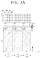
- FIG. 5A illustrates a schematic view illustrating an optical element and an LED, according to an exemplary embodiment.
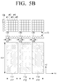
- FIG. 5B illustrates a schematic view illustrating an optical element and an LED, according to another exemplary embodiment.
- FIG. 5C illustrates a schematic view illustrating an optical element and an LED, according to yet another exemplary embodiment.
- an LED i.e., a full pixel
- a red LED 11r a green LED 11g
- a blue LED 11b a red LED 11r
- a red LED 11r a green LED 11g
- a blue LED 11b a blue LED 11b
- An optical element 13 may correspond to each of the red LED 11r, the green LED 11g and the blue LED 11b, i.e., sub-pixels.
- the red LED 11r, the green LED 11g and the blue LED 11b, i.e., sub-pixels, may be positioned to correspond to a round-shaped unit lens 13a repetitively formed on the optical element 13.
- a plurality of unit lenses 13a may correspond to one sub-pixel 11r (e.g., red LED).
- a red LED will be described as an example, and features applicable to the red LED 11r may be applied to other sub-pixels as well.
- a width 11r (e.g., +x axis direction) of the red LED 11r, which is one of sub-pixels of a full pixel, LED 11, may, for example, be 300 ⁇ m.
- the above-described width of a sub-pixel is described as an example, but it would be easily understood by those skilled in the art that the example is not limited thereto.
- a width I2r (or pitch) of a unit lens 13a corresponding to a width I1r of the red LED 11r of the optical element 13 may vary according to exemplary embodiments.
- the width I2r may be less than or equal to 1/6 of the width I1r of the red LED 11r.
- the width I2r of the unit lens 13a may be less than or equal to one 1/5 of a width I1r of the red LED 11r.
- a width I2r of a unit lens 13a may be in the range of 20 ⁇ m to 50 ⁇ m.
- the width I2r of a unit lens 13a may be in the range of 11 ⁇ m to 40 ⁇ m.
- the width I2r of a unit lens 13a may be in the range of 30 ⁇ m to 60 ⁇ m.
- a width I1g of a green LED 11g which is one of sub-pixels of the LED, may, for example, be 300 ⁇ m.
- a width I2g of a unit lens 13a corresponding to a width I1g of the green LED 11g of the optical element 13 may vary according to exemplary embodiments. For example, a width I2g may be less than or equal to 1/6 of the width I1g of the green LED 11g.
- a width I2g of a unit lens 13a may be less than or equal to one fifth of a width I1g of a green LED 11g.
- a width I2g of a unit lens 13a may be in the range of 20 ⁇ m to 50 ⁇ m.
- a width I2g of a unit lens 13a may be in the range of 11 ⁇ m to 40 ⁇ m.
- a width I2g of a unit lens 13a may be in the range of 30 ⁇ m to 60 ⁇ m.
- a width I1b of the blue LED 11b which is one of sub-pixels of a full pixel, LED 11, may, for example, be 300 ⁇ m.
- Awidth I2r of a unit lens 13a corresponding to a width I1b of the blue LED 11b may vary according to exemplary embodiments.
- the width I2b may be less than or equal to 1/6 of the width I1b of the blue LED 11 b.
- the width I2b of the unit lens 13a may be less than or equal to one fifth of a width I1b of the blue LED 11 b.
- the width I2b of a unit lens 13a may be in the range of 20 ⁇ m to 50 ⁇ m.
- the width I2b of a unit lens 13a may be in the range of 11 ⁇ m to 40 ⁇ m.
- the width I2b of a unit lens 13a may be in the range of 30 ⁇ m to 60 ⁇ m.
- a unit lens 13a of the optical element 13 may be repetitively formed to correspond to a dimension (for example, width X length (height)) of an LED module 10.
- a pitch between unit lenses 13a of the optical element 13 may be formed to correspond to a pitch between the sub-pixels, i.e., the red LED 11r, the green LED 11g, and the blue LED.
- a pitch between a plurality of unit lenses corresponding to the red LED 11r and a plurality of unit lenses corresponding to the green LED 11g may be formed to correspond to a pitch between the red LED 11r and the green LED 11g.
- a pitch between a plurality of unit lenses corresponding to the green LED 11g and a plurality of unit lenses corresponding to the blue LED 11b may be formed to correspond to a pitch between the green LED 11g and the blue LED 11b.
- a pitch between a plurality of unit lenses corresponding to the blue LED 11b and a plurality of unit lenses corresponding to the red LED 11r may be formed to correspond to a pitch between the blue LED 11 b and the red LED 11 r.
- a pitch between unit lenses 13a of the optical element may be formed to correspond to a pitch between an LED 11, which is a full pixel, and another adjacent LED.
- a pitch between a plurality of unit lenses corresponding to one LED 11 and a plurality of unit lenses corresponding to the next LED may be formed to correspond to a pitch between one LED 11 and a next LED positioned in a traverse direction (e.g., +x axis direction).
- a pitch between a plurality of unit lenses corresponding to one LED 11 and a plurality of unit lenses corresponding to the next LED may be formed to correspond to a pitch between one LED 11 and a next LED positioned in a longitudinal direction (e.g., +/-z axis direction).
- a dimension (e.g., height, width or area) of a unit lens 13a of the optical element 13 may be formed differently according to a pitch between the red LED 11 r, the green LED 11g and the blue LED 11b, i.e., sub-pixels.
- a dimension (e.g., height, width or area) of the unit lens 13a may be different according to positions.
- a dimension of unit lenses #1 and #5 positioned at the edges of the five unit lenses may be larger than a dimension of a unit lens #3 positioned in the center.
- a dimension of unit lenses #1 and #5 positioned at the edges of the five unit lenses may be larger than dimensions of adjacent unit lenses #2 and #4.
- dimensions of a plurality of unit lenses #2, #3 and #4 from among the five unit lenses may be the same.
- a dimension (e.g., height, width or area) of the unit lens 13a may be different according to positions.
- a dimension of unit lenses #1 and #6 positioned at the edges of the six unit lenses may be larger than dimensions of unit lenses #3 and #4 positioned in the center.
- Dimensions of a plurality of unit lenses #2, #3, #4 and #5 from among the six unit lenses may be the same.
- a color split which occurs when only one unit lens 13a corresponds to one sub-pixel 11r, may be reduced.
- a height (i.e., a length on the z axis) of the red LED 11r, which is one of sub-pixels of a full pixel, LED 11, may, for example, be 1,000 ⁇ m ⁇ m.
- the above-described height of a sub-pixel is described as an example, but it would be easily understood by those skilled in the art that the example is not limited thereto.
- a width I2r (or pitch) of a unit lens 13a may be determined depending on a height h1r of the red LED 11r of the optical element 13. For example, the width I2r may be less than or equal to one eighteenth of the height h1r of the red LED 11r. For another example, the width I2r of the unit lens 13a may be less than or equal to one fifteenth of a height h1r of the red LED 11r. As a result, for example, the width I2r may be in the range of 20 ⁇ m to 50 ⁇ m. For another example, the width I2r of a unit lens 13a may be in the range of 11 ⁇ m to 40 ⁇ m. For another example, the width I2r of a unit lens 13a may be in the range of 30 ⁇ m to 60 ⁇ m.
- a unit lens 13a of the optical element 13 may be repetitively formed based on a dimension (for example, width X length (height)) of an LED module 10.
- a pitch between unit lenses 13a of the optical element 13 may be formed to correspond to a pitch between the sub-pixels, e.g., between a red LED 11r and another red LED in an adjacent direction (e.g., +/- z axis direction).
- a pitch between a plurality of unit lenses corresponding to the red LED 11 r and a plurality of unit lenses corresponding to another adjacent red LED may be formed to correspond to a pitch between the red LED 11r r and the another red Led positioned in a +z axis direction.
- a pitch between a plurality of unit lenses corresponding to the red LED 11 r and a plurality of unit lenses corresponding to another adjacent red LED may be formed to correspond to a pitch between the red LED 11r and the another red Led positioned in a -z axis direction.
- unit lenses 13a are described taking an example of a width direction (e.g., x axis direction). However, it would be easily understood by one of ordinary skill in the art that the same may apply to a height direction (e.g., z axis direction) of the LED 11.
- an LED 11, i.e., a full pixel, may be implemented with a plurality of sub-pixels, e.g., a red LED 11r', a green LED 11 g', and a blue LED 11b'.
- An optical element 13 may correspond to each of the red LED 11r', the green LED 11g' and the blue LED 11b', i.e., sub-pixels, may be implemented.
- the red LED 11r', the green LED 11g' and the blue LED 11b', i.e., sub-pixels, may be positioned to correspond to a round-shaped unit lens 13b repetitively formed on the optical element 13.
- a plurality of unit lenses 13b may correspond to one sub-pixel 11 r' (e.g., red LED).
- a plurality of unit lenses 13b may correspond to a red LED 11 r' (which is described as an example, and the same applies to other sub-pixels as well), which is one sub-pixel.
- a width I1r' of a red LED 11 r' may be, for example, 300 ⁇ m.
- a width I2r' (or pitch) of a triangle-shaped unit lens 13b may vary according to exemplary embodiments.
- the width I2r' may be less than or equal to 1/6 of the width I1r' of the red LED 11 r'.
- the width I2r' of the unit lens 13b may be less than or equal to 1/5 of the width I1r' of the red LED 11r'.
- the width I2r' of a unit lens 13b may be in the range of 20 ⁇ m to 50 ⁇ m.
- a width I1g' of a green LED 11g' may be, as a non-limiting example, 300 ⁇ m.
- a width I2g' of a unit lens 13b may vary according to exemplary embodiments. For example, the width I2g' may be less than or equal to 1/6 of the width I1g' of the green LED 11g'. For another example, the width I2g' of a unit lens 13b may be less than or equal to 1/5 of the width I1g' of the green LED 11g'. As a result, for example, the width I2g' of a unit lens 13b may be in the range of 20 ⁇ m to 50 ⁇ m.
- a width I1b' of a blue LED 11 b' may be, as a non-limiting example, 300 ⁇ m.
- a width I2b' of a unit lens 13b corresponding to a width I1b' of a blue LED 11 b' may vary according to exemplary embodiments.
- the width I2b' may be less than or equal to 1/6 of the width I1b' of the blue LED 11 b'.
- the width I2b' of the unit lens 13b may be less than or equal to 1/5 of a width I1b' of the blue LED 11b'.
- the width I2b' of the unit lens 13b may be in the range of 20 ⁇ m to 50 ⁇ m.
- a unit lens 13b of the optical element 13 may be repetitively formed to correspond to a dimension (e.g., width X length (height)) of an LED module 10.
- a pitch between unit lenses 13b of the optical element 13 may be formed to correspond to a pitch between the sub-pixels, i.e., the red LED 11r', the green LED 11g', and the blue LED 11b'.
- a pitch between a plurality of triangle-shaped unit lenses corresponding to the red LED 11r' and a plurality of triangle-shaped unit lenses corresponding to the green LED 11g' may be formed to correspond to a pitch between the red LED 11r' and the green LED 11g'.
- a pitch between a plurality of triangle-shaped unit lenses corresponding to the green LED 11g' and a plurality of triangle-shaped unit lenses corresponding to the blue LED 11 b' may be formed to correspond to a pitch between the green LED 11g' and the blue LED 11b'.
- a pitch between a plurality of triangle-shaped unit lenses corresponding to the blue LED 11b' and a plurality of triangle-shaped unit lenses corresponding to the red LED 11 r' may be formed to correspond to a pitch between the blue LED 11 b' and the red LED 11 r'.
- a pitch between unit lenses 13b of the optical element 13 may be formed to correspond to a pitch between an LED 11, which is a full pixel, and another adjacent LED.
- a pitch between a plurality of unit lenses corresponding to one LED 11 and a plurality of unit lenses corresponding to the next LED may be formed to correspond to a pitch between one LED 11 and a next LED positioned in a traverse direction (e.g., x-axis direction).
- a pitch between a plurality of unit lenses corresponding to one LED 11 and a plurality of unit lenses corresponding to the next LED may be formed to correspond to a pitch between one LED 11 and a next LED positioned in a longitudinal direction (e.g., z axis direction).
- a dimension (e.g., height, width or area) of a unit lens 13a of the optical element 13 may be formed differently according to a pitch between the red LED 11r', the green LED 11g' and the blue LED 11b', i.e., sub-pixels.
- a dimension of the unit lens 13b may be different according to positions.
- a dimension of unit lenses #1 and #5 positioned at the edges of the five unit lenses may be larger than a dimension of a unit lens #3 positioned in the center.
- a dimension of unit lenses #1 and #5 positioned at the edges of the five unit lenses may be larger than dimensions of adjacent unit lenses #2 and #4.
- dimensions of a plurality of unit lenses #2, #3 and #4 from among the five unit lenses may be the same.
- a dimension of the unit lens 13b may be different according to positions.
- a dimension of unit lenses #1 and #6 positioned at the edges of the six unit lenses may be larger than dimensions of unit lenses #3 and #4 positioned in the center.
- Dimensions of a plurality of unit lenses #2, #3, #4 and #5 from among the six unit lenses may be the same.
- a color split which occurs when only one unit lens 13b corresponds to one sub-pixel 11r', may be reduced.
- unit lenses 13b were described taking an example of a width direction (e.g., x axis direction). However, it would be easily understood by one of ordinary skill in the art that the same may apply to a height direction (e.g., z axis direction) of the LED 11.
- the description of the sub-pixels, the red LED 11r', the green LED 11g', and the blue LED 11 b' corresponding to a triangle-shaped unit lens 13b of FIG. 5B will be omitted herein, since it is substantially similar (i.e., only a shape of unit lens is different) to the description of the sub-pixels, the red LED 11 r, the green LED 11g, and the blue LED 11b of FIG. 5A .
- an LED 11, i.e., a full pixel, may be implemented with a plurality of sub-pixels, e.g., a red LED 11r', a green LED 11g', and a blue LED 11b'.
- An optical element 13 may correspond to each of the red LED 11r", the green LED 11g" and the blue LED 11b", i.e., sub-pixels, may be implemented.
- the red LED 11r", the green LED 11g” and the blue LED 11b" may be positioned to correspond to a triangle-shaped unit lens 13c that has round corners and is repetitively formed on the optical element 13.
- a plurality of triangle-shaped unit lenses 13c having round corners may correspond to one sub-pixel 11r" (i.e., red LED).
- a width I1r" of a red LED 11 r" may be, for example, 300 ⁇ m.
- a width I2r" (or pitch) of a triangle-shaped unit lens 13c of the optical element 13 may vary according to exemplary embodiments.
- the width I2r" may be less than or equal to 1/6 of the width I1r" of the red LED 11r".
- the width I2r" of the unit lens 13c may be less than or equal to 1/5 of the width I1r" of the red LED 11 r".
- the width I2r" of a unit lens 13c may be in the range of 20 ⁇ m to 50 ⁇ m.
- a width I1g" of a green LED 11g" may be, as a non-limiting example, 300 ⁇ m.
- a width I2g" of a unit lens 13c of the optical element 13 may vary according to exemplary embodiments. For example, the width I2g" may be less than or equal to 1/6 of the width I1g" of the green LED 11g". Further, a width I2g" of a unit lens 13c may be less than or equal to 1/5 of a width I1g" of a green LED 11g". As a result, for example, the width I2g" of a unit lens 13c may be in the range of 20 ⁇ m to 50 ⁇ m.
- a width I1b" of a blue LED 11b" may be, as a non-limiting example, 300 ⁇ m.
- a width I2b" of a unit lens 13c of the optical element 13 may vary according to exemplary embodiments.
- the width I2b" may be less than or equal to 1/6 of the width I1b" of the blue LED 11b".
- the width I2b" of the unit lens 13c may be less than or equal to 1/5 of a width I1b" of the blue LED 11b".
- the width I2b" of a unit lens 13c may be in the range of 20 ⁇ m to 50 ⁇ m.
- a unit lens 13c of the optical element 13 may be repetitively formed to correspond to a dimension (e.g., width X length (height)) of an LED module 10.
- a pitch between unit lenses 13c of the optical element 13 may be formed to correspond to a pitch between the sub-pixels, i.e., the red LED 11r", the green LED 11g", and the blue LED 11b".
- a pitch between a plurality of triangle-shaped unit lenses having round corners which correspond to the red LED 11 r" and a plurality of triangle-shaped unit lenses having round corners which correspond to the green LED 11g" may be formed to correspond to a pitch between the red LED 11r" and the green LED 11g".
- a pitch between a plurality of triangle-shaped unit lenses having round corners which correspond to the green LED 11g" and a plurality of triangle-shaped unit lenses having round corners which correspond to the blue LED 11 b" may be formed to correspond to a pitch between the green LED 11g" and the blue LED 11b".
- a pitch between a plurality of triangle-shaped unit lenses having round corners which correspond to the blue LED 11b" and a plurality of triangle-shaped unit lenses having round corners which correspond to the red LED 11r" may be formed to correspond to a pitch between the blue LED 11 b" and the red LED 11 r".
- a pitch between unit lenses 13c of the optical element 13 may be formed to correspond to a pitch between an LED 11, which is a full pixel, and another adjacent LED.
- a pitch between a plurality of unit lenses corresponding to one LED 11 and a plurality of unit lenses corresponding to the next LED may be formed to correspond to a pitch between one LED 11 and a next LED positioned in a traverse direction (e.g., x-axis direction).
- a pitch between a plurality of unit lenses corresponding to one LED 11 and a plurality of unit lenses corresponding to the next LED may be formed to correspond to a pitch between one LED 11 and a next LED positioned in a longitudinal direction (e.g., z axis direction).
- a dimension (e.g., height, width or area) of a unit lens 13a of the optical element 13 may be formed differently according to a pitch between the red LED 11r", the green LED 11g" and the blue LED 11b", i.e., sub-pixels.
- a dimension of the unit lens 13c may be different according to positions.
- a dimension of unit lenses #1 and #5 positioned at the edges of the five unit lenses may be larger than a dimension of a unit lens #3 positioned in the center.
- a dimension of unit lenses #1 and #5 positioned at the edges of the five unit lenses may be larger than dimensions of adjacent unit lenses #2 and #4.
- dimensions of a plurality of unit lenses #2, #3 and #4 from among the five unit lenses may be the same.
- a dimension of the unit lens 13c may be different according to positions.
- a dimension of unit lenses #1 and #6 positioned at the edges of the six unit lenses may be larger than dimensions of unit lenses #3, #4 positioned in the center.
- Dimensions of a plurality of unit lenses #2, #3, #4 and #5 from among the six unit lenses may be the same.
- a color split which occurs when only one unit lens 13c corresponds to one sub-pixel 11 r" may be reduced.
- unit lenses 13c were described taking an example of a width direction (e.g., x axis direction). However, it would be easily understood by one of ordinary skill in the art that the same may apply to a height direction (e.g., z axis direction) of the LED 11.
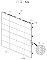
- FIG. 6A illustrates a front perspective view of an LED display apparatus according to another exemplary embodiment.
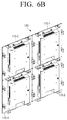
- FIG. 6B illustrates a rear perspective view of an LED display apparatus according to yet another exemplary embodiment.
- an LED display apparatus 100 may include a plurality of LED panels 110 (e.g., 110-1 to 110-4).
- the LED panel 110 may be triangular, quadrilateral (for example, rectangle or square) or polygonal.
- the plurality of LED panels 110 may be connected to each other in a matrix form (for example, M*N, in which M and N are natural numbers).
- the size of arrays in the matrix may be the same (e.g., 2*2 or 4*4) or different from each other.
- a plurality of LED panels (e.g., 110-1 to 110-4) may be connected to each other using a link bracket 124 (see FIG. 2B ) and a coupling member (e.g., bolt, rivet, or etc.).
- a timing controller of each of the LED panels 110-1 to 110-4 may generate video data (or image data) and a control signal corresponding to video (or image) received from an external control device, and may transmit the generated video data and control signal to each of LEDs 11 of the LED panels 110-1 to 110-4.
- the LED display apparatus 100 may display content (e.g., video, image, or etc.) by driving each of the LEDs 11 of the LED panels 110-1 to 110-4.
- content e.g., video, image, or etc.
- An external control device may transmit video data and a control signal corresponding to the content to the LEDs 110-1 to 110-4.
- the external control device may transmit video data and a control signal corresponding to the content to the LEDs 110-1 to 110-4 at one time.
- the aforementioned methods according to exemplary embodiments may be implemented as a program command executable by various computer means, and the program command may be stored in a non-transitory computer-readable medium.
- the computer-readable medium may include a program command, a data file, a data structure, etc., taken alone or in combination.
- the computer-readable medium may be recorded on a volatile or non-volatile storage device such as ROM, etc., or for example, a memory such as RAM, a memory chip, a device or an integrated circuit, or may be recorded optically or magnetically such as a CD, DVD, a magnetic disk or magnetic tape, etc.
- the computer-readable medium may be stored in a storage medium readable by a machine (e.g., computer).
- a memory that may be included in a mobile terminal is an example of a program including instructions to implement the exemplary embodiments or a storage medium that is readable using an appropriate machine.
- a program command recorded on the medium may be specially designed and configured for the present disclosure or may be made public to one of ordinary skill in the art of computer software.
Landscapes
- Engineering & Computer Science (AREA)
- Physics & Mathematics (AREA)
- General Physics & Mathematics (AREA)
- General Engineering & Computer Science (AREA)
- Theoretical Computer Science (AREA)
- Microelectronics & Electronic Packaging (AREA)
- Optics & Photonics (AREA)
- Business, Economics & Management (AREA)
- Accounting & Taxation (AREA)
- Marketing (AREA)
- Multimedia (AREA)
- Led Device Packages (AREA)
- Devices For Indicating Variable Information By Combining Individual Elements (AREA)
Applications Claiming Priority (1)
| Application Number | Priority Date | Filing Date | Title |
|---|---|---|---|
| KR1020150142130A KR102396325B1 (ko) | 2015-10-12 | 2015-10-12 | 엘이디 디스플레이 장치의 광학 부재 및 엘이디 디스플레이 장치 |
Publications (2)
| Publication Number | Publication Date |
|---|---|
| EP3156991A1 true EP3156991A1 (fr) | 2017-04-19 |
| EP3156991B1 EP3156991B1 (fr) | 2020-11-04 |
Family
ID=56896406
Family Applications (1)
| Application Number | Title | Priority Date | Filing Date |
|---|---|---|---|
| EP16188050.5A Not-in-force EP3156991B1 (fr) | 2015-10-12 | 2016-09-09 | Élément optique de dispositif d'affichage à del et dispositif d'affichage à del |
Country Status (4)
| Country | Link |
|---|---|
| US (1) | US20170102485A1 (fr) |
| EP (1) | EP3156991B1 (fr) |
| KR (1) | KR102396325B1 (fr) |
| WO (1) | WO2017065474A1 (fr) |
Cited By (2)
| Publication number | Priority date | Publication date | Assignee | Title |
|---|---|---|---|---|
| RU187208U1 (ru) * | 2017-11-10 | 2019-02-25 | Юнилумин Груп Ко., Лтд. | Соединительная конструкция для светодиодных устройств отображения |
| EP3811414A4 (fr) * | 2018-08-20 | 2021-08-18 | Samsung Electronics Co., Ltd. | Appareil d'affichage et son procédé de fabrication |
Families Citing this family (6)
| Publication number | Priority date | Publication date | Assignee | Title |
|---|---|---|---|---|
| CN107610605A (zh) * | 2017-09-26 | 2018-01-19 | 上海欧美拉光电股份有限公司 | 一种led可编程天幕屏 |
| KR102219936B1 (ko) * | 2018-08-23 | 2021-02-25 | 삼성전자주식회사 | 디스플레이 장치 |
| CN109584745A (zh) * | 2018-12-12 | 2019-04-05 | 四川兴煌科技有限公司 | 一种灯箱三面翻棱柱结构 |
| CN109982481A (zh) * | 2019-03-15 | 2019-07-05 | 冠捷显示科技(厦门)有限公司 | 一种有助于助眠的显示设备及其助眠方法 |
| KR102785122B1 (ko) | 2019-08-13 | 2025-03-26 | 삼성전자주식회사 | 디스플레이 장치 및 그의 제조 방법 |
| KR102268755B1 (ko) * | 2019-09-30 | 2021-06-24 | 엘지전자 주식회사 | 디스플레이 장치 |
Citations (6)
| Publication number | Priority date | Publication date | Assignee | Title |
|---|---|---|---|---|
| EP1645800A2 (fr) * | 2004-10-07 | 2006-04-12 | Barco, naamloze vennootschap. | Système et procédé d'amélioration optique des éléments vidéo et des éléments d'éclairages |
| CN202075944U (zh) * | 2011-05-26 | 2011-12-14 | 夏志清 | Led显示屏模组 |
| EP2717244A1 (fr) * | 2012-03-26 | 2014-04-09 | Dai Nippon Printing Co., Ltd. | Dispositif d'affichage de type de réseau |
| CN104049374A (zh) * | 2014-07-05 | 2014-09-17 | 福州大学 | 一种可实现面发光的led屏及其裸眼立体显示装置 |
| CA2903265A1 (fr) * | 2013-03-14 | 2014-09-18 | Leyard Optoelectronic Co., Ltd. | Dispositif d'affichage a del |
| CN104680947A (zh) * | 2015-02-15 | 2015-06-03 | 北京环宇蓝博科技有限公司 | Led屏幕消除莫尔条纹并提高填充系数的装置及方法 |
Family Cites Families (18)
| Publication number | Priority date | Publication date | Assignee | Title |
|---|---|---|---|---|
| US6130777A (en) * | 1996-05-16 | 2000-10-10 | Dai Nippon Printing Co., Ltd. | Lenticular lens sheet with both a base sheet having lenticular elements and a surface diffusing part having elements of elementary shape smaller than lenticular elements |
| US6809470B2 (en) * | 2000-12-29 | 2004-10-26 | Intel Corporation | Flat panel color display with enhanced brightness and preferential viewing angles |
| JP2003330111A (ja) * | 2002-05-10 | 2003-11-19 | Olympus Optical Co Ltd | 発光ユニット、照明装置、及び投影表示装置 |
| JP2007012323A (ja) * | 2005-06-28 | 2007-01-18 | Cheil Ind Co Ltd | 面光源装置及び液晶表示装置 |
| JP2008020532A (ja) * | 2006-07-11 | 2008-01-31 | Fujifilm Corp | 光学機能性シート及び表示装置 |
| KR20080040878A (ko) * | 2006-11-06 | 2008-05-09 | 삼성전자주식회사 | 광학렌즈 플레이트, 백라이트 유닛 및 이를 구비하는표시장치 |
| KR100981960B1 (ko) * | 2008-09-09 | 2010-09-14 | 지엘레페주식회사 | 평판형 엘이디 조명등 |
| JP4678058B2 (ja) * | 2009-01-14 | 2011-04-27 | ソニー株式会社 | 光制御部材、発光装置および表示装置 |
| WO2011086719A1 (fr) * | 2010-01-15 | 2011-07-21 | 凸版印刷株式会社 | Corps de guidage de lumière, structure de dissimulation, et dispositif d'éclairage et appareil d'affichage le comportant |
| KR101707607B1 (ko) * | 2010-03-04 | 2017-02-17 | 삼성디스플레이 주식회사 | 표시장치 |
| KR101211723B1 (ko) * | 2010-09-20 | 2012-12-12 | 엘지이노텍 주식회사 | 광학용시트, 광학유닛 및 이를 적용한 조명장치 |
| CN101936476B (zh) * | 2010-09-24 | 2013-06-05 | 鸿富锦精密工业(深圳)有限公司 | 三色混光led点光源装置 |
| JP5740901B2 (ja) * | 2010-10-15 | 2015-07-01 | ソニー株式会社 | 発光装置および表示装置 |
| JP5877992B2 (ja) * | 2010-10-25 | 2016-03-08 | 株式会社半導体エネルギー研究所 | 表示装置 |
| KR102127973B1 (ko) * | 2013-09-23 | 2020-06-29 | 엘지디스플레이 주식회사 | 백라이트 유닛 및 이를 이용한 디스플레이 장치 |
| KR20150051774A (ko) * | 2013-11-05 | 2015-05-13 | 영남대학교 산학협력단 | Led 라이트 박스 |
| US9983337B2 (en) * | 2015-08-07 | 2018-05-29 | Samsung Electronics Co., Ltd. | Light emitting diode display apparatus |
| US10032757B2 (en) * | 2015-09-04 | 2018-07-24 | Hong Kong Beida Jade Bird Display Limited | Projection display system |
-
2015
- 2015-10-12 KR KR1020150142130A patent/KR102396325B1/ko active Active
-
2016
- 2016-09-09 EP EP16188050.5A patent/EP3156991B1/fr not_active Not-in-force
- 2016-09-15 US US15/266,582 patent/US20170102485A1/en not_active Abandoned
- 2016-10-11 WO PCT/KR2016/011356 patent/WO2017065474A1/fr not_active Ceased
Patent Citations (6)
| Publication number | Priority date | Publication date | Assignee | Title |
|---|---|---|---|---|
| EP1645800A2 (fr) * | 2004-10-07 | 2006-04-12 | Barco, naamloze vennootschap. | Système et procédé d'amélioration optique des éléments vidéo et des éléments d'éclairages |
| CN202075944U (zh) * | 2011-05-26 | 2011-12-14 | 夏志清 | Led显示屏模组 |
| EP2717244A1 (fr) * | 2012-03-26 | 2014-04-09 | Dai Nippon Printing Co., Ltd. | Dispositif d'affichage de type de réseau |
| CA2903265A1 (fr) * | 2013-03-14 | 2014-09-18 | Leyard Optoelectronic Co., Ltd. | Dispositif d'affichage a del |
| CN104049374A (zh) * | 2014-07-05 | 2014-09-17 | 福州大学 | 一种可实现面发光的led屏及其裸眼立体显示装置 |
| CN104680947A (zh) * | 2015-02-15 | 2015-06-03 | 北京环宇蓝博科技有限公司 | Led屏幕消除莫尔条纹并提高填充系数的装置及方法 |
Cited By (2)
| Publication number | Priority date | Publication date | Assignee | Title |
|---|---|---|---|---|
| RU187208U1 (ru) * | 2017-11-10 | 2019-02-25 | Юнилумин Груп Ко., Лтд. | Соединительная конструкция для светодиодных устройств отображения |
| EP3811414A4 (fr) * | 2018-08-20 | 2021-08-18 | Samsung Electronics Co., Ltd. | Appareil d'affichage et son procédé de fabrication |
Also Published As
| Publication number | Publication date |
|---|---|
| KR20170043127A (ko) | 2017-04-21 |
| EP3156991B1 (fr) | 2020-11-04 |
| WO2017065474A1 (fr) | 2017-04-20 |
| US20170102485A1 (en) | 2017-04-13 |
| KR102396325B1 (ko) | 2022-05-13 |
Similar Documents
| Publication | Publication Date | Title |
|---|---|---|
| EP3156991B1 (fr) | Élément optique de dispositif d'affichage à del et dispositif d'affichage à del | |
| US11054871B2 (en) | Display device including radiant heat blocking layer | |
| JP6261505B2 (ja) | 湾曲したベゼル隠蔽ディスプレイ装置カバーおよびベゼルのないディスプレイ装置 | |
| KR20180011983A (ko) | 엘이디 디스플레이 장치의 결합 구조 및 엘이디 디스플레이 장치 | |
| EP2431653A1 (fr) | Dispositif d éclairage et dispositif d affichage | |
| US10996508B2 (en) | Liquid crystal display device | |
| KR102463679B1 (ko) | Led 디스플레이 | |
| KR100751722B1 (ko) | 광고판 | |
| JP2021528700A (ja) | 混合フォーマットバックライト、ディスプレイ、および方法 | |
| CN110780364B (zh) | 光控膜和包括该光控膜的显示装置 | |
| KR20190069030A (ko) | 디스플레이 장치 및 그 제어 방법 | |
| US20120133606A1 (en) | Display For Digital Images | |
| EP3703132A1 (fr) | Dispositif d'affichage à del | |
| KR20130019250A (ko) | 백라이트 유닛 및 이를 구비한 액정표시장치 | |
| CN101620325A (zh) | 显示器 | |
| WO2012026163A1 (fr) | Dispositif d'éclairage, dispositif d'affichage et dispositif de téléviseur | |
| KR102347472B1 (ko) | 양면 표시장치 및 그를 위한 백라이트 유닛 | |
| CN211426960U (zh) | 一种透明显示器及一种显示系统 | |
| WO2025035941A1 (fr) | Module d'affichage | |
| TWI624691B (zh) | 透明自動立體顯示器 | |
| WO2012026162A1 (fr) | Dispositif d'éclairage, dispositif d'affichage et dispositif de téléviseur | |
| JP2013218922A (ja) | バックライト装置、表示装置、及びテレビ受信装置 | |
| JP2013175288A (ja) | バックライト装置、表示装置、及びテレビ受信装置 | |
| KR101321248B1 (ko) | 엘이디 패널의 고휘도화 개조를 위한 광학 필름의 적층 구조 | |
| WO2012176697A1 (fr) | Dispositif de rétroéclairage, dispositif d'affichage et récepteur de télévision |
Legal Events
| Date | Code | Title | Description |
|---|---|---|---|
| PUAI | Public reference made under article 153(3) epc to a published international application that has entered the european phase |
Free format text: ORIGINAL CODE: 0009012 |
|
| STAA | Information on the status of an ep patent application or granted ep patent |
Free format text: STATUS: THE APPLICATION HAS BEEN PUBLISHED |
|
| STAA | Information on the status of an ep patent application or granted ep patent |
Free format text: STATUS: REQUEST FOR EXAMINATION WAS MADE |
|
| AK | Designated contracting states |
Kind code of ref document: A1 Designated state(s): AL AT BE BG CH CY CZ DE DK EE ES FI FR GB GR HR HU IE IS IT LI LT LU LV MC MK MT NL NO PL PT RO RS SE SI SK SM TR |
|
| AX | Request for extension of the european patent |
Extension state: BA ME |
|
| 17P | Request for examination filed |
Effective date: 20170404 |
|
| RBV | Designated contracting states (corrected) |
Designated state(s): AL AT BE BG CH CY CZ DE DK EE ES FI FR GB GR HR HU IE IS IT LI LT LU LV MC MK MT NL NO PL PT RO RS SE SI SK SM TR |
|
| STAA | Information on the status of an ep patent application or granted ep patent |
Free format text: STATUS: EXAMINATION IS IN PROGRESS |
|
| 17Q | First examination report despatched |
Effective date: 20191114 |
|
| GRAP | Despatch of communication of intention to grant a patent |
Free format text: ORIGINAL CODE: EPIDOSNIGR1 |
|
| STAA | Information on the status of an ep patent application or granted ep patent |
Free format text: STATUS: GRANT OF PATENT IS INTENDED |
|
| INTG | Intention to grant announced |
Effective date: 20200514 |
|
| GRAS | Grant fee paid |
Free format text: ORIGINAL CODE: EPIDOSNIGR3 |
|
| GRAA | (expected) grant |
Free format text: ORIGINAL CODE: 0009210 |
|
| STAA | Information on the status of an ep patent application or granted ep patent |
Free format text: STATUS: THE PATENT HAS BEEN GRANTED |
|
| AK | Designated contracting states |
Kind code of ref document: B1 Designated state(s): AL AT BE BG CH CY CZ DE DK EE ES FI FR GB GR HR HU IE IS IT LI LT LU LV MC MK MT NL NO PL PT RO RS SE SI SK SM TR |
|
| REG | Reference to a national code |
Ref country code: GB Ref legal event code: FG4D |
|
| REG | Reference to a national code |
Ref country code: CH Ref legal event code: EP |
|
| REG | Reference to a national code |
Ref country code: AT Ref legal event code: REF Ref document number: 1331828 Country of ref document: AT Kind code of ref document: T Effective date: 20201115 |
|
| REG | Reference to a national code |
Ref country code: IE Ref legal event code: FG4D |
|
| REG | Reference to a national code |
Ref country code: DE Ref legal event code: R096 Ref document number: 602016047026 Country of ref document: DE |
|
| REG | Reference to a national code |
Ref country code: NL Ref legal event code: MP Effective date: 20201104 |
|
| REG | Reference to a national code |
Ref country code: AT Ref legal event code: MK05 Ref document number: 1331828 Country of ref document: AT Kind code of ref document: T Effective date: 20201104 |
|
| PG25 | Lapsed in a contracting state [announced via postgrant information from national office to epo] |
Ref country code: PT Free format text: LAPSE BECAUSE OF FAILURE TO SUBMIT A TRANSLATION OF THE DESCRIPTION OR TO PAY THE FEE WITHIN THE PRESCRIBED TIME-LIMIT Effective date: 20210304 Ref country code: RS Free format text: LAPSE BECAUSE OF FAILURE TO SUBMIT A TRANSLATION OF THE DESCRIPTION OR TO PAY THE FEE WITHIN THE PRESCRIBED TIME-LIMIT Effective date: 20201104 Ref country code: NO Free format text: LAPSE BECAUSE OF FAILURE TO SUBMIT A TRANSLATION OF THE DESCRIPTION OR TO PAY THE FEE WITHIN THE PRESCRIBED TIME-LIMIT Effective date: 20210204 Ref country code: FI Free format text: LAPSE BECAUSE OF FAILURE TO SUBMIT A TRANSLATION OF THE DESCRIPTION OR TO PAY THE FEE WITHIN THE PRESCRIBED TIME-LIMIT Effective date: 20201104 Ref country code: GR Free format text: LAPSE BECAUSE OF FAILURE TO SUBMIT A TRANSLATION OF THE DESCRIPTION OR TO PAY THE FEE WITHIN THE PRESCRIBED TIME-LIMIT Effective date: 20210205 |
|
| PG25 | Lapsed in a contracting state [announced via postgrant information from national office to epo] |
Ref country code: SE Free format text: LAPSE BECAUSE OF FAILURE TO SUBMIT A TRANSLATION OF THE DESCRIPTION OR TO PAY THE FEE WITHIN THE PRESCRIBED TIME-LIMIT Effective date: 20201104 Ref country code: AT Free format text: LAPSE BECAUSE OF FAILURE TO SUBMIT A TRANSLATION OF THE DESCRIPTION OR TO PAY THE FEE WITHIN THE PRESCRIBED TIME-LIMIT Effective date: 20201104 Ref country code: ES Free format text: LAPSE BECAUSE OF FAILURE TO SUBMIT A TRANSLATION OF THE DESCRIPTION OR TO PAY THE FEE WITHIN THE PRESCRIBED TIME-LIMIT Effective date: 20201104 Ref country code: BG Free format text: LAPSE BECAUSE OF FAILURE TO SUBMIT A TRANSLATION OF THE DESCRIPTION OR TO PAY THE FEE WITHIN THE PRESCRIBED TIME-LIMIT Effective date: 20210204 Ref country code: IS Free format text: LAPSE BECAUSE OF FAILURE TO SUBMIT A TRANSLATION OF THE DESCRIPTION OR TO PAY THE FEE WITHIN THE PRESCRIBED TIME-LIMIT Effective date: 20210304 Ref country code: PL Free format text: LAPSE BECAUSE OF FAILURE TO SUBMIT A TRANSLATION OF THE DESCRIPTION OR TO PAY THE FEE WITHIN THE PRESCRIBED TIME-LIMIT Effective date: 20201104 Ref country code: LV Free format text: LAPSE BECAUSE OF FAILURE TO SUBMIT A TRANSLATION OF THE DESCRIPTION OR TO PAY THE FEE WITHIN THE PRESCRIBED TIME-LIMIT Effective date: 20201104 |
|
| REG | Reference to a national code |
Ref country code: LT Ref legal event code: MG9D |
|
| PG25 | Lapsed in a contracting state [announced via postgrant information from national office to epo] |
Ref country code: HR Free format text: LAPSE BECAUSE OF FAILURE TO SUBMIT A TRANSLATION OF THE DESCRIPTION OR TO PAY THE FEE WITHIN THE PRESCRIBED TIME-LIMIT Effective date: 20201104 |
|
| PG25 | Lapsed in a contracting state [announced via postgrant information from national office to epo] |
Ref country code: RO Free format text: LAPSE BECAUSE OF FAILURE TO SUBMIT A TRANSLATION OF THE DESCRIPTION OR TO PAY THE FEE WITHIN THE PRESCRIBED TIME-LIMIT Effective date: 20201104 Ref country code: SK Free format text: LAPSE BECAUSE OF FAILURE TO SUBMIT A TRANSLATION OF THE DESCRIPTION OR TO PAY THE FEE WITHIN THE PRESCRIBED TIME-LIMIT Effective date: 20201104 Ref country code: CZ Free format text: LAPSE BECAUSE OF FAILURE TO SUBMIT A TRANSLATION OF THE DESCRIPTION OR TO PAY THE FEE WITHIN THE PRESCRIBED TIME-LIMIT Effective date: 20201104 Ref country code: EE Free format text: LAPSE BECAUSE OF FAILURE TO SUBMIT A TRANSLATION OF THE DESCRIPTION OR TO PAY THE FEE WITHIN THE PRESCRIBED TIME-LIMIT Effective date: 20201104 Ref country code: SM Free format text: LAPSE BECAUSE OF FAILURE TO SUBMIT A TRANSLATION OF THE DESCRIPTION OR TO PAY THE FEE WITHIN THE PRESCRIBED TIME-LIMIT Effective date: 20201104 Ref country code: LT Free format text: LAPSE BECAUSE OF FAILURE TO SUBMIT A TRANSLATION OF THE DESCRIPTION OR TO PAY THE FEE WITHIN THE PRESCRIBED TIME-LIMIT Effective date: 20201104 |
|
| REG | Reference to a national code |
Ref country code: DE Ref legal event code: R097 Ref document number: 602016047026 Country of ref document: DE |
|
| PG25 | Lapsed in a contracting state [announced via postgrant information from national office to epo] |
Ref country code: DK Free format text: LAPSE BECAUSE OF FAILURE TO SUBMIT A TRANSLATION OF THE DESCRIPTION OR TO PAY THE FEE WITHIN THE PRESCRIBED TIME-LIMIT Effective date: 20201104 |
|
| PLBE | No opposition filed within time limit |
Free format text: ORIGINAL CODE: 0009261 |
|
| STAA | Information on the status of an ep patent application or granted ep patent |
Free format text: STATUS: NO OPPOSITION FILED WITHIN TIME LIMIT |
|
| 26N | No opposition filed |
Effective date: 20210805 |
|
| PG25 | Lapsed in a contracting state [announced via postgrant information from national office to epo] |
Ref country code: NL Free format text: LAPSE BECAUSE OF FAILURE TO SUBMIT A TRANSLATION OF THE DESCRIPTION OR TO PAY THE FEE WITHIN THE PRESCRIBED TIME-LIMIT Effective date: 20201104 Ref country code: IT Free format text: LAPSE BECAUSE OF FAILURE TO SUBMIT A TRANSLATION OF THE DESCRIPTION OR TO PAY THE FEE WITHIN THE PRESCRIBED TIME-LIMIT Effective date: 20201104 Ref country code: AL Free format text: LAPSE BECAUSE OF FAILURE TO SUBMIT A TRANSLATION OF THE DESCRIPTION OR TO PAY THE FEE WITHIN THE PRESCRIBED TIME-LIMIT Effective date: 20201104 |
|
| PG25 | Lapsed in a contracting state [announced via postgrant information from national office to epo] |
Ref country code: SI Free format text: LAPSE BECAUSE OF FAILURE TO SUBMIT A TRANSLATION OF THE DESCRIPTION OR TO PAY THE FEE WITHIN THE PRESCRIBED TIME-LIMIT Effective date: 20201104 |
|
| REG | Reference to a national code |
Ref country code: DE Ref legal event code: R119 Ref document number: 602016047026 Country of ref document: DE |
|
| REG | Reference to a national code |
Ref country code: CH Ref legal event code: PL |
|
| REG | Reference to a national code |
Ref country code: BE Ref legal event code: MM Effective date: 20210930 |
|
| GBPC | Gb: european patent ceased through non-payment of renewal fee |
Effective date: 20210909 |
|
| PG25 | Lapsed in a contracting state [announced via postgrant information from national office to epo] |
Ref country code: IS Free format text: LAPSE BECAUSE OF FAILURE TO SUBMIT A TRANSLATION OF THE DESCRIPTION OR TO PAY THE FEE WITHIN THE PRESCRIBED TIME-LIMIT Effective date: 20210304 Ref country code: MC Free format text: LAPSE BECAUSE OF FAILURE TO SUBMIT A TRANSLATION OF THE DESCRIPTION OR TO PAY THE FEE WITHIN THE PRESCRIBED TIME-LIMIT Effective date: 20201104 |
|
| PG25 | Lapsed in a contracting state [announced via postgrant information from national office to epo] |
Ref country code: LU Free format text: LAPSE BECAUSE OF NON-PAYMENT OF DUE FEES Effective date: 20210909 Ref country code: IE Free format text: LAPSE BECAUSE OF NON-PAYMENT OF DUE FEES Effective date: 20210909 Ref country code: GB Free format text: LAPSE BECAUSE OF NON-PAYMENT OF DUE FEES Effective date: 20210909 Ref country code: FR Free format text: LAPSE BECAUSE OF NON-PAYMENT OF DUE FEES Effective date: 20210930 Ref country code: DE Free format text: LAPSE BECAUSE OF NON-PAYMENT OF DUE FEES Effective date: 20220401 Ref country code: BE Free format text: LAPSE BECAUSE OF NON-PAYMENT OF DUE FEES Effective date: 20210930 |
|
| PG25 | Lapsed in a contracting state [announced via postgrant information from national office to epo] |
Ref country code: LI Free format text: LAPSE BECAUSE OF NON-PAYMENT OF DUE FEES Effective date: 20210930 Ref country code: CH Free format text: LAPSE BECAUSE OF NON-PAYMENT OF DUE FEES Effective date: 20210930 |
|
| PG25 | Lapsed in a contracting state [announced via postgrant information from national office to epo] |
Ref country code: HU Free format text: LAPSE BECAUSE OF FAILURE TO SUBMIT A TRANSLATION OF THE DESCRIPTION OR TO PAY THE FEE WITHIN THE PRESCRIBED TIME-LIMIT; INVALID AB INITIO Effective date: 20160909 |
|
| PG25 | Lapsed in a contracting state [announced via postgrant information from national office to epo] |
Ref country code: CY Free format text: LAPSE BECAUSE OF FAILURE TO SUBMIT A TRANSLATION OF THE DESCRIPTION OR TO PAY THE FEE WITHIN THE PRESCRIBED TIME-LIMIT Effective date: 20201104 |
|
| PG25 | Lapsed in a contracting state [announced via postgrant information from national office to epo] |
Ref country code: MK Free format text: LAPSE BECAUSE OF FAILURE TO SUBMIT A TRANSLATION OF THE DESCRIPTION OR TO PAY THE FEE WITHIN THE PRESCRIBED TIME-LIMIT Effective date: 20201104 |
|
| PG25 | Lapsed in a contracting state [announced via postgrant information from national office to epo] |
Ref country code: TR Free format text: LAPSE BECAUSE OF FAILURE TO SUBMIT A TRANSLATION OF THE DESCRIPTION OR TO PAY THE FEE WITHIN THE PRESCRIBED TIME-LIMIT Effective date: 20201104 |
|
| PG25 | Lapsed in a contracting state [announced via postgrant information from national office to epo] |
Ref country code: MT Free format text: LAPSE BECAUSE OF FAILURE TO SUBMIT A TRANSLATION OF THE DESCRIPTION OR TO PAY THE FEE WITHIN THE PRESCRIBED TIME-LIMIT Effective date: 20201104 |