EP3157111B1 - Dispositif de test, procédé de test, et programme de commande de protection de réseau électrique - Google Patents
Dispositif de test, procédé de test, et programme de commande de protection de réseau électrique Download PDFInfo
- Publication number
- EP3157111B1 EP3157111B1 EP14894334.3A EP14894334A EP3157111B1 EP 3157111 B1 EP3157111 B1 EP 3157111B1 EP 14894334 A EP14894334 A EP 14894334A EP 3157111 B1 EP3157111 B1 EP 3157111B1
- Authority
- EP
- European Patent Office
- Prior art keywords
- data
- information
- testing device
- characteristic
- intelligent electronic
- Prior art date
- Legal status (The legal status is an assumption and is not a legal conclusion. Google has not performed a legal analysis and makes no representation as to the accuracy of the status listed.)
- Active
Links
Images





Classifications
-
- G—PHYSICS
- G01—MEASURING; TESTING
- G01R—MEASURING ELECTRIC VARIABLES; MEASURING MAGNETIC VARIABLES
- G01R31/00—Arrangements for testing electric properties; Arrangements for locating electric faults; Arrangements for electrical testing characterised by what is being tested not provided for elsewhere
- G01R31/50—Testing of electric apparatus, lines, cables or components for short-circuits, continuity, leakage current or incorrect line connections
- G01R31/62—Testing of transformers
-
- G—PHYSICS
- G01—MEASURING; TESTING
- G01R—MEASURING ELECTRIC VARIABLES; MEASURING MAGNETIC VARIABLES
- G01R35/00—Testing or calibrating of apparatus covered by the other groups of this subclass
-
- G—PHYSICS
- G01—MEASURING; TESTING
- G01R—MEASURING ELECTRIC VARIABLES; MEASURING MAGNETIC VARIABLES
- G01R19/00—Arrangements for measuring currents or voltages or for indicating presence or sign thereof
- G01R19/25—Arrangements for measuring currents or voltages or for indicating presence or sign thereof using digital measurement techniques
- G01R19/2513—Arrangements for monitoring electric power systems, e.g. power lines or loads; Logging
-
- H—ELECTRICITY
- H02—GENERATION; CONVERSION OR DISTRIBUTION OF ELECTRIC POWER
- H02H—EMERGENCY PROTECTIVE CIRCUIT ARRANGEMENTS
- H02H3/00—Emergency protective circuit arrangements for automatic disconnection directly responsive to an undesired change from normal electric working condition with or without subsequent reconnection ; integrated protection
- H02H3/02—Details
- H02H3/05—Details with means for increasing reliability, e.g. redundancy arrangements
-
- H—ELECTRICITY
- H02—GENERATION; CONVERSION OR DISTRIBUTION OF ELECTRIC POWER
- H02H—EMERGENCY PROTECTIVE CIRCUIT ARRANGEMENTS
- H02H7/00—Emergency protective circuit arrangements specially adapted for specific types of electric machines or apparatus or for sectionalised protection of cable or line systems, and effecting automatic switching in the event of an undesired change from normal working conditions
- H02H7/04—Emergency protective circuit arrangements specially adapted for specific types of electric machines or apparatus or for sectionalised protection of cable or line systems, and effecting automatic switching in the event of an undesired change from normal working conditions for transformers
-
- H—ELECTRICITY
- H02—GENERATION; CONVERSION OR DISTRIBUTION OF ELECTRIC POWER
- H02H—EMERGENCY PROTECTIVE CIRCUIT ARRANGEMENTS
- H02H7/00—Emergency protective circuit arrangements specially adapted for specific types of electric machines or apparatus or for sectionalised protection of cable or line systems, and effecting automatic switching in the event of an undesired change from normal working conditions
- H02H7/04—Emergency protective circuit arrangements specially adapted for specific types of electric machines or apparatus or for sectionalised protection of cable or line systems, and effecting automatic switching in the event of an undesired change from normal working conditions for transformers
- H02H7/042—Emergency protective circuit arrangements specially adapted for specific types of electric machines or apparatus or for sectionalised protection of cable or line systems, and effecting automatic switching in the event of an undesired change from normal working conditions for transformers for current transformers
Definitions
- the present invention relates to a testing device for testing an intelligent electronic device, which is configured to (i) acquire at least information of current or voltage from a power system, (ii) detect failure in the power system, a power facility, or the like, and (iii) separate the failure from the power system.
- an intelligent electronic device is configured to (i) acquire results of measurement of voltage value and current value in the power system from a current transformer (CT), a potential transformer (PT) (or voltage transformer (VT)), and the like, (ii) detect occurrence of overvoltage, shortage of voltage, overcurrent, or the like due to failure or the like, and (iii) send a control signal to a circuit breaker. Accordingly, a countermeasure can be immediately taken by, for example, separating the failed section from the power system.
- CT current transformer
- PT potential transformer
- VT voltage transformer
- the intelligent electronic device Since such an intelligent electronic device requires high reliability, the intelligent electronic device is subjected to various performance check tests in various aspects, for example, before shipment or during service.
- Patent Document 1 describes a digital protective power relay device having a testing function.
- a digital relay is provided with a memory in which data of voltage waveform or current waveform corresponding to power system failure and input conditions such as device conditions in the power system side are written beforehand.
- This digital protective power relay device is provided with a switch, which is externally switchable to read out either (i) an amount of analog input acquired from the power system side or (ii) the waveform data written in the memory.
- the relay device is verified by: switching the switch to the side of the memory having the waveform data written therein; sequentially reading out the waveform data from the memory at a sampling cycle of the protective relay; and performing calculation for the relay in accordance with the data thus read out. Accordingly, a similar effect is obtained as with the case of externally applying current and voltage waveforms for simulating power system failure by utilizing a simulation power transmission line.
- Patent Document 2 describes the following technique: in a power system protection control system employing a process bus, for the purpose of a test, a testing device is connected to the process bus, and the testing device outputs, to an intelligent electronic device via the process bus, test electric quantity information having a test flag added therein. Based on the test electric quantity information received from the testing device, the intelligent electronic device determines whether to trip a circuit breaker. If it is determined to trip, the intelligent electronic device outputs to the process bus a test trip command having the test flag added therein. When a merging unit (MU) receives the test trip command via the process bus, the merging unit determines that the operation of the intelligent electronic device outputting the trip command is normal.
- MU merging unit
- PEICHAO ZHANG ET AL "Compatibility and interoperability evaluation for all-digital protection system through automatic application test”
- 2006 IEEE POWER ENGINEERING SOCIETY GENERAL MEETING 18-22 June 2006
- page 7 proposes a methodology of compatibility and interoperability evaluation for all-digital protection systems through automatic application testing.
- CHRISTOPH BRUNNER ET AL "Functional Testing of IEC 61850 based systems", PAC World magazine, 15 January 2011, pages 1-5 provides a broad overview of the IEC 61850 standard and compatible systems.
- the data of the prepared memory which has the voltage waveform data and current waveform data corresponding to the power system failure and the information of the devices in the power system, is used for the test, so that the intelligent electronic device includes hardware necessary for the test but unnecessary for normal service. Accordingly, the intelligent electronic device becomes expensive, and percent defective may become high due to the inclusion of the hardware unnecessary for normal service, disadvantageously.
- the technique described in Patent Document 2 is directed to checking whether or not the intelligent electronic device in service is normal. Therefore, the technique described in Patent Document 2 is not sufficient to comprehensively check performance before starting service by, for example, determining whether or not the intelligent electronic device is applicable to the power system, or determining whether to connect the MU and the intelligent electronic device when combining the MU and the intelligent electronic device in the power system protection control system.
- an intelligent electronic device and an MU may be provided by different manufacturers, so that it is important to comprehensively check performance by connecting the intelligent electronic device and the MU before starting service.
- various devices are used for instrument transformers.
- the instrument transformers may include: an iron-core CT; an ECT (Electric CT) employing an air-core CT (Rogowski CT); and a CVT (Capacitance VT) employing a capacitor to divide voltage into small voltage. Therefore, characteristics of CTs and PTs, such as frequency characteristic and transient characteristic, may greatly differ among the CTs and PTs.
- an object of the present disclosure is to provide a testing device capable of simulating comprehensive check in advance with regard to performance attained when installing an intelligent electronic device in a power system.
- a testing device as set out in claim 1 is provided, a testing method as set out in claim 11 is provided, and a program as set out in claim 12 is provided.
- the testing device acquires failure data resulting from simulation calculation for a CT and a PT and simulation calculation for an MU, the simulation calculation for the CT and the PT being performed with respect to current waveform data and voltage waveform data in the power system based on a characteristic of an instrument transformer, the simulation calculation for the MU being performed with respect to the current waveform data and voltage waveform data in the power system based on a characteristic of the MU.
- the testing device acquires device information data in synchronization with the failure data, the device information data indicating a circuit breaker of the power system.
- the testing device transmits the failure data and device information data to the intelligent electronic device via the process bus in accordance with a setting of outputting data to the process bus and a setting of sampling.
- comprehensive performance check can be simulated in advance before applying the intelligent electronic device and the MU to protection control of the power system because the failure data, which results from (i) the simulation calculation for the CT and the PT based on the characteristics of the instrument transformers and (ii) the simulation calculation for the MU according to the characteristic of the MU, is transmitted to the intelligent electronic device in synchronization with the device data. This reduces a possibility of occurrence of a problem due to connection with the MU and the intelligent electronic device after starting service.
- a protection control system including a testing device (TEST-MU (Merging Unit)) in accordance with a first embodiment.
- Fig. 1 shows an entire configuration of a protection control system 1 including a testing device in accordance with the present embodiment.
- protection control system 1 is provided in a substation, a power distribution station, or the like to collect information of the power system and to perform processes such as protection, control, and monitoring of the power system based on the collected information.
- protection control system 1 includes: a plurality of merging units 10-1, 10-2 (hereinafter, also collectively referred to as “merging unit 10") each configured to collect information, such as current and voltage, from the power system; and a plurality of intelligent electronic devices 20-1 to 20-N (hereinafter, also abbreviated as “IED” and also collectively referred to as “intelligent electronic device 20”) configured to protect, control, and monitor the power system.
- Data communication can be made between merging units 10-1 to 10-5 and intelligent electronic devices 20-1 to 20-N via a process bus 22.
- the plurality of intelligent electronic devices 20 are disposed based on purposes of use (for example, based on targets of protection or based on targets of control). Examples of the IEDs thus disposed based on the purposes of use include: a protective IED configured to implement a protective function; and a control IED configured to implement a control function.
- Each merging unit 10 sends (i) the information collected from the power system to (ii) an intelligent electronic device 20 corresponding to that merging unit 10. Based on the information received from corresponding merging unit 10, each of intelligent electronic devices 20 performs a process such as protection, control, or monitoring of the power system.
- intelligent electronic device 20 determines, at a predetermined cycle, whether or not a relay calculation logic set in advance is established, and outputs a trip signal to a corresponding circuit breaker when the relay calculation logic is established.
- This trip signal may be transmitted via process bus 22.
- intelligent electronic device 20 can output a command to close/open a switch in the power system, for example.
- monitoring function if some power system failure occurs, intelligent electronic device 20 can log information of the power system before and after the occurrence of the power system failure, and can output the state of the power system in real time.
- intelligent electronic device 20 is connected to a substation automation system (SAS) device 26 and a remote monitoring control device 28 via a station bus 24.
- intelligent electronic device 20 can output the information of the power system to substation automation system device 26, and also can output the information of the power system to a remote control center 30, which is distant away from the power facility of interest, via remote monitoring control device 28.
- intelligent electronic device 20 can be configured to implement intended processes other than the processes described above.
- intelligent electronic device 20 may be utilized to implement a function equivalent to substation automation system device 26.
- a circuit breaker 6-1 In a power transmission line 2, a circuit breaker 6-1, a current transformer (CT) 7-1, and a potential transformer (PT) (/voltage transformer (VT)) 8-1 are provided.
- Current transformer 7-1 measures information (current waveform) of current flowing through power transmission line 2.
- Potential transformer 8-1 measures information (voltage waveform) of voltage generated in power transmission line 2.
- merging unit 10-1 collects (i) the information of the current flowing through power transmission line 2 and (ii) the information of the voltage generated in power transmission line 2.
- a circuit breaker 6-2 in a supply line 4, a circuit breaker 6-2, a current transformer 7-2, and a potential transformer 8-2 are provided. Respective pieces of information measured by current transformer 7-2 and potential transformer 8-2 are sent to merging unit 10-2.
- the current transformers may be also collectively referred to as "current transformer 7”.
- the potential transformers may be also collectively referred to as “potential transformer 8”.
- the circuit breakers may be also collectively referred to as "circuit breaker 6".
- Merging unit 10-1 receives device information (DI) of circuit breaker 6-1.
- merging unit 10-2 receives device information (DI) of circuit breaker 6-2.
- Each merging unit 10 converts the received data into digital data.
- the serial data thus output to process bus 22 is received by intelligent electronic device 20 connected to process bus 22.
- Intelligent electronic device 20 uses the received serial data to perform protection control calculation in order to determine whether or not the power system is failed. If it is determined that the power system is failed, intelligent electronic device 20 outputs a trip command to a circuit breaker associated with the failure, thereby separating the failure point from the power system.
- testing device 50 of the first embodiment is connected to process bus 22. Moreover, testing device 50 is connected to a PC (Personal Computer) 60, which is a general-purpose information processing device, via a general-purpose input/output IF (interface), for example.
- PC Personal Computer
- IF input/output
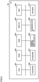
- Fig. 2 shows a functional configuration of merging unit 10.
- a measured value (analog signal) from an instrument transformer (CT, PT) provided in the power transmission line, the bus, or the like is sent to merging unit 10.
- Merging unit 10 collects current information and/or voltage information of the power system, and outputs digital data indicating the collected information to intelligent electronic device 20.
- pieces of information necessary for protection, control, monitoring, and the like of the power system are collected in merging unit 10. Examples of this digital data typically include serial data in which measured values are arranged in series in the order of sampling times.
- Merging unit 10 receives current waveform signal and/or voltage waveform signal of the power system, digitally converts the current waveform signal and/or voltage waveform signal, and then outputs the digitally converted current waveform signal and/or voltage waveform signal via process bus 22 as serial data.
- Merging unit 10 includes an isolation transformer 11, an analog filter 12, an AD (Analog to Digital) conversion circuit 13, a data buffer memory circuit 14, a process bus IF circuit 15, a reception circuit 16, a sampling control circuit 17, a data reading circuit 18, and an isolation circuit 19.
- Isolation transformer 11 receives at least one of (i) a current waveform measured by current transformer 7 and (ii) a voltage waveform measured by potential transformer 8. The data received from current transformer 7 or potential transformer 8 is isolated by isolation transformer 11, and is converted by an internal circuit of merging unit 10 to have an appropriate voltage signal level.
- Analog filter 12 removes a high-frequency noise component superimposed on the received current waveform or voltage waveform.
- AD conversion circuit 13 converts the analog input signal into digital data in accordance with a sampling control signal from sampling control circuit 17, and data buffer memory circuit 14 holds the converted digital data therein.
- Isolation circuit 19 receives device information (DI) indicating circuit breaker 6 or the like, and converts the received signal into a signal having a certain voltage.
- DI device information
- Data reading circuit 18 holds the signal converted by isolation circuit 19 and reads the device information (DI) in accordance with the sampling control signal from sampling control circuit 17, and then data buffer memory circuit 14 holds the device information (DI).
- Reception circuit 16 receives a time synchronization signal from an external system (for example, GPS (Global Positioning System)) and outputs it to sampling control circuit 17.
- an external system for example, GPS (Global Positioning System)
- Sampling control circuit 17 receives the time synchronization signal from reception circuit 16, and outputs a sampling control signal indicating a timing of sampling to AD conversion circuit 13, data buffer memory circuit 14, process bus IF circuit 15, and data reading circuit 18.
- Data buffer memory circuit 14 holds (i) the digitally converted data of the received current waveform or voltage waveform, and (ii) the device information to be synchronized with this data.
- data buffer memory circuit 14 converts the held data into data compliant with a protocol defined in process bus 22, and outputs the resulting data to process bus 22 via process bus IF circuit 15.
- Process bus IF circuit 15 is an interface configured to sequentially output data to process bus 22 as serial data.
- Fig. 3 is a block diagram showing a configuration of PC 60.
- PC 60 includes a CPU (Central Processing Unit) 601, a ROM (Read Only Memory) 602, a RAM (Random Access Memory) 603, a display 604, a microphone 605, a touchpad 606, a keyboard 607, a general-purpose input/output IF 608, a communication IF 609, and a speaker 610.
- CPU Central Processing Unit
- ROM Read Only Memory
- RAM Random Access Memory
- CPU 601 executes various types of programs including an OS (Operating System) to control operation of PC 60.
- ROM 602 stores BIOS (Basic Input/Output System) and various types of data.
- RAM 603 provides a work area for storing data necessary for CPU 601 to execute a program.
- Display 604 displays various types of information.
- HDD (Hard Disk Drive) 605 stores a program or the like in a nonvolatile manner.
- Touchpad 606 which is an operation member configured to receive a user's input operation, receives the user's touch as an input operation by detecting the user's touch by way of a capacitive method, for example.
- Keyboard 607 which is an operating member configured to receive the user's input operation, receives a key input from the user.
- General-purpose input/output IF 608, which is a general-purpose input/output interface such as a USB (Universal Serial Bus), serves as an interface configured to provide connection to an external device.
- Communication IF 609 is an interface for communication in compliance with a LAN (Local Area Network) standard or the like.
- Speaker 610 outputs sound in accordance with control of CPU 601.
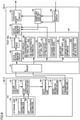
- Fig. 4 shows the configuration of testing device 50 and the functional configuration of PC 60.
- PC 60 includes a failure calculation unit 61, a CT&PT characteristic simulation unit 62, an MU characteristic simulation unit 63, a data transmission unit 64, a device information generation unit 65, a TEST-MU transmission setting unit 66, and a storage unit 67.
- Storage unit 67 stores: (i) CT characteristic information 621 indicating characteristic(s) of a CT, such as a type of the CT, a frequency characteristic of the CT, and/or a transient characteristic of the CT; (ii) PT characteristic information 622 indicating characteristic(s) of a PT, such as a type of the PT and/or a transient characteristic of the PT; and (iii) MU characteristic information 623 indicating characteristic(s) of an MU, such as a filter characteristic of the MU and/or a dynamic range of the MU.
- CT characteristic information 621 indicating characteristic(s) of a CT, such as a type of the CT, a frequency characteristic of the CT, and/or a transient characteristic of the CT
- PT characteristic information 622 indicating characteristic(s) of a PT, such as a type of the PT and/or a transient characteristic of the PT
- MU characteristic information 623 indicating characteristic(s) of an MU, such as a filter
- Failure calculation unit 61 performs calculation with respect to current waveform data and voltage waveform data obtained from the CT and the PT in the power system.
- failure calculation unit 61 is configured to beforehand hold current waveform data and voltage waveform data corresponding to failure in the power system, or is configured to receive such current waveform data and voltage waveform data corresponding to failure in the power system.
- CT&PT characteristic simulation unit 62 performs simulation calculation to simulate the characteristics of the CT and the PT in accordance with (i) the characteristic of the CT indicated by CT characteristic information 621 and (ii) the characteristic of the PT indicated by PT characteristic information 622.
- MU characteristic simulation unit 63 performs simulation calculation to simulate the characteristic of the MU such as the filter characteristic of the MU in accordance with the characteristic of the MU indicated by MU characteristic information 623.
- PC 60 generates, as failure data, data corresponding to a period of time necessary to verify failure in the power system (for example, data corresponding to a period of time of about several hundred milliseconds to several seconds).
- Data transmission unit 64 transmits, to testing device 50, the failure data obtained by MU characteristic simulation unit 63, and an IF circuit 51 of testing device 50 receives the failure data, which is then stored into a data buffer circuit 52 of testing device 50.
- device information generation unit 65 generates, in synchronization with the failure data, device information (DI) indicating circuit breaker 6 (specifically, to change circuit breaker 6 from the close state to the open state after passage of certain time from power system failure, for example), and data transmission unit 64 transmits the generated device information (DI), which is then stored into data buffer circuit 52 together with the failure data.
- DI device information
- TEST-MU transmission setting unit 66 holds transmission setting information (TEST-MU transmission setting information) for causing testing device 50 to output data to process bus 22. This transmission setting information is then stored into a setting circuit 54 of testing device 50 via IF circuit 51. Examples of the transmission setting information include: (i) PB data output setting information 811, which is information indicating a setting value of current or voltage value per bit for testing device 50 to output serial data to process bus 22; and (ii) dynamic range information 812 indicating a dynamic range of the current or voltage for testing device 50 to output data through a process bus IF circuit 53.
- Another example of the transmission setting information is a setting about sampling for testing device 50 to output serial data to process bus 22, such as: sampling frequency information 821 indicating a frequency of sampling; or a time synchronization method setting 822 indicating a setting of a time synchronization method in accordance with the time synchronization information received by testing device 50 from the outside.
- Testing device 50 includes IF circuit 51, data buffer circuit 52, process bus IF circuit 53, setting circuit 54, a reception circuit 55, and a sampling control circuit 56.
- IF circuit 51 exhibits a function as an interface for providing connection with PC 60.
- Data buffer circuit 52 receives the failure data and the device information from PC 60 and holds them, and outputs them to process bus 22 via process bus IF circuit 53 in accordance with information of a sampling cycle provided from sampling control circuit 56.
- Process bus IF circuit 53 outputs the data held by data buffer circuit 52 to process bus 22 as serial data in accordance with (i) the information of the sampling cycle provided from sampling control circuit 56, (ii) the current and voltage values per bit of the output data set by setting circuit 54, or the like.
- Setting circuit 54 is a circuit configured to receive various types of data from PC 60 and hold them therein, and set a method of outputting the data from testing device 50.
- Setting circuit 54 includes an output data setting unit 81 and a sampling setting unit 82.
- Output data setting unit 81 receives information such as PB data output setting information 811 and dynamic range information 812 from PC 60, and sets process bus IF circuit 53 in accordance with settings indicated in these pieces of information so as to cause process bus IF circuit 53 to output the serial data.
- sampling setting unit 82 receives information such as sampling frequency information 821 and time synchronization method setting 822, and sets sampling control circuit 56 in accordance with settings of the sampling indicated in these pieces of information so as to cause process bus IF circuit 53 to output serial data.
- Reception circuit 55 receives a time synchronization signal from outside, and outputs the received time synchronization signal to sampling control circuit 56.
- Sampling control circuit 56 outputs a sampling control signal to process bus IF circuit 53 and data buffer circuit 52 based on (i) the setting of the sampling set by sampling setting unit 82 and (ii) the time synchronization signal received from reception circuit 55, thereby controlling the output of the serial data to process bus 22 by testing device 50.
- Testing device 50 is configured to acquire the failure data resulting from the simulation calculation for the CT and the PT and the simulation calculation for the MU, the simulation calculation for the CT and the PT being performed with respect to the current waveform data and voltage waveform data in the power system based on the characteristic information (CT characteristic information 621 and PT characteristic information 622) indicating the characteristic of the instrument transformer, the simulation calculation for the MU being performed with respect to the current waveform data and voltage waveform data in the power system based on the characteristic information (MU characteristic information 623) indicating the characteristic of the MU.
- This configuration is implemented by IF circuit 51 and data buffer memory circuit 52.
- testing device 50 is configured to acquire the device information data (DI) indicating the circuit breaker of the power system, in synchronization with the failure data.
- DI device information data
- Testing device 50 is configured to transmit the failure data and the device information data (DI) to intelligent electronic device 20 via process bus 22.
- DI device information data
- This configuration is implemented by setting circuit 54, data buffer memory circuit 52, process bus IF circuit 53, and sampling control circuit 56.
- Fig. 5 is a flowchart showing operations of PC 60 and testing device 50.
- failure calculation unit 61 acquires at least one of the current waveform data and voltage waveform data corresponding to the case where the power system is failed.
- CT&PT characteristic simulation unit 62 performs simulation calculation according to the characteristics of the CT and the PT based on CT characteristic information 621 and PT characteristic information 622.
- MU characteristic simulation unit 63 In a step S605, in PC 60, MU characteristic simulation unit 63 generates failure data by performing, with respect to the data resulting from the simulation calculation performed in step S603, simulation calculation according to the characteristic of the MU based on MU characteristic information 623.
- device information generation unit 65 In a step S607, in PC 60, device information generation unit 65 generates device information (DI) of the circuit breaker or the like in synchronization with the failure data generated in step S605.
- DI device information
- data transmission unit 64 transmits the failure data and the device information (DI) to testing device 50, and data transmission unit 64 transmits, to testing device 50, transmission setting information for causing testing device 50 to output the serial data to process bus 22, and then the transmission setting information is held in setting circuit 54.
- DI device information
- testing device 50 receives the failure data and the device information (DI) from PC 60, and stores them into data buffer circuit 52.
- Testing device 50 holds, in output data setting unit 81 and sampling setting unit 82, the transmission setting information received from PC 60, reads the failure data and the device information (DI) from data buffer circuit 52 in accordance with the setting indicated in the transmission setting information, and outputs them to intelligent electronic device 20 via process bus 22 as the serial data.
- intelligent electronic device 20 receives the failure data and the device information (DI), and performs protection calculation.
- testing device 50 in protection control system 1, it is possible to perform (i) the simulation of the power system failure inclusive of the simulation according to the characteristics of the CT and the PT and (ii) the simulation according to the characteristic of the MU to be actually connected to the power system, whereby before connecting the MU and the IED to the power system, an operation characteristic can be checked as to whether a problem or the like occurs due to the connection with the MU and the IED. This ensures highly reliable verification, which also leads to reduction of test cost and test time. Moreover, since the simulation calculation for the MU is performed by PC 60, no current amplifier, voltage amplifier and the like are required.
- the characteristic of the MU is simulated by testing device 50 in the second embodiment, while the characteristic of the MU is simulated by PC 60 in the first embodiment.
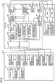
- Fig. 6 shows a configuration of a testing device 50-2 and a functional configuration of a PC 60-2 in the second embodiment.
- data transmission unit 64 in PC 60-2 of the second embodiment transmits, to testing device 50, the current waveform data and voltage waveform data obtained by CT&PT characteristic simulation unit 62 and resulting from the simulation calculation according to the characteristics of the CT and the PT, and then data buffer memory circuit 58 of testing device 50 holds the current waveform data and voltage waveform data therein.
- TEST-MU transmission setting unit 66 which holds MU characteristic information 623 indicating the characteristic of the MU, transmits MU characteristic information 623 to testing device 50, and then MU characteristic setting unit 83 of setting circuit 54 holds MU characteristic information 623 therein.
- calculation circuit 57 receives, from MU characteristic setting unit 83 of setting circuit 54, a setting of the simulation calculation according to the characteristic of the MU.
- Calculation circuit 57 performs simulation calculation with respect to the current waveform data and voltage waveform data held in data buffer memory circuit 58 based on MU characteristic information 623, so as to simulate the characteristic of the MU such as the filter characteristic of the MU.
- Calculation circuit 57 holds, in data buffer circuit 52, data resulting from the simulation calculation for simulating the characteristic of the MU.
- the characteristic of the MU is simulated by testing device 50.
- Fig. 7 is a flowchart showing operations of PC 60-2 and testing device 50-2 in the second embodiment.
- device information generation unit 65 In a step S608, in PC 60, device information generation unit 65 generates the device information (DI) of the circuit breaker or the like in synchronization with the data resulting from the simulation calculation in step S603.
- DI device information
- data transmission unit 64 transmits, to testing device 50, (i) the data resulting from the simulation calculation in step S603 and (ii) the device information (DI), so as to hold them in data buffer memory circuit 58; and data transmission unit 64 transmits, to testing device 50, (i) the transmission setting information for causing testing device 50 to output the serial data to process bus 22 and (ii) the MU characteristic information, so as to hold them in setting circuit 54.
- DI device information
- testing device 50 receives (i) the data resulting from the simulation calculation in step S603 (the current waveform data and voltage waveform data that simulates the characteristics of the CT and the PT) and (ii) the device information (DI) and stores them into data buffer memory circuit 58, and receives the transmission setting information and the MU characteristic information and stores them into the memory of setting circuit 54.
- the data resulting from the simulation calculation in step S603 the current waveform data and voltage waveform data that simulates the characteristics of the CT and the PT
- DI device information
- calculation circuit 57 In a step S515, in testing device 50, calculation circuit 57 generates the failure data by performing the simulation calculation with respect to the current waveform data and voltage waveform data stored in data buffer memory circuit 58 based on the characteristic of the MU so as to simulate the characteristic of the MU, and data buffer circuit 52 holds the generated failure data therein.
- testing device 50 outputs, to intelligent electronic device 20 via process bus 22 as the serial data, the failure data and device information (DI) stored in data buffer circuit 52 in accordance with the setting indicated in the transmission setting information.
- DI failure data and device information
- the simulation calculation for the MU according to the characteristic of the MU is performed in testing device 50. Therefore, when the MU is replaced (with an MU manufactured by a different manufacturer, for example), the calculation results of the current waveform data and voltage waveform data calculated by PC 60 can be used without any modification because testing device 50 acquires, from PC 60 or the like, the information (such as MU characteristic information 623) necessary for the simulation of the MU.
- testing device 50 acquires operation information of intelligent electronic device 20 via a station bus 24 and accordingly determines whether or not operation of intelligent electronic device 20 is normal.
- the operation of intelligent electronic device 20 can be checked automatically, thereby resulting in efficient operation check.
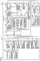
- Fig. 8 shows a configuration of a testing device 50-3, a functional configuration of a PC 60-3, and a configuration of intelligent electronic device 20 in the third embodiment.
- Intelligent electronic device 20 includes a PBIF (process bus IF) 201, a protection control calculation unit 202, an output processing unit 203, and an SBIF (station bus IF) 204.
- PBIF 201 is an interface configured to receive, via process bus 22, the data output to process bus 22 by testing device 50.
- Protection control calculation unit 202 performs protection calculation based on the failure data or the like received by PBIF 201, and outputs the result of protection calculation to output processing unit 203.
- Output processing unit 203 generates output data for outputting, to testing device 50 via station bus 24, the result of the protection calculation performed by protection control calculation unit 202, in accordance with a protocol defined in the station bus.
- SBIF 204 outputs the output data to station bus 24.
- PC 60 includes an IED determination value transmission unit 68 and an IED determination result collection unit 69.
- IED determination value transmission unit 68 transmits, to testing device 50, a determination value to be compared with the result of the protection calculation performed by intelligent electronic device 20.
- IED determination result collection unit 69 receives and collects, from testing device 50, a result of comparison between the determination value and the result of the protection calculation performed by intelligent electronic device 20.
- Testing device 50 includes an SBIF circuit 59, an IED determination value setting unit 84, and a determination circuit 90.
- IED determination value setting unit 84 receives and holds the determination value transmitted by IED determination value transmission unit 68 of PC 60, and sets the determination value at determination circuit 90.
- SBIF circuit 59 receives data via station bus 24.
- Determination circuit 90 compares (i) the result of the protection calculation of intelligent electronic device 20 received by SBIF circuit 59 with (ii) the determination value set by IED determination value setting unit 84. When the result of protection calculation and the determination value fall within a certain range, determination circuit 90 determines that the calculated result of intelligent electronic device 20 is normal. Otherwise, determination circuit 90 determines that the calculated result of intelligent electronic device 20 is not normal and transmits the determination result to PC 60 via IF circuit 51.
- the determination result provided by testing device 50-3 is collected by PC 60-3, but may be collected by testing device 50-3.
- Fig. 9 shows a configuration of a testing device 50-4, a functional configuration of a PC 60-4, and a configuration of intelligent electronic device 20 in the fourth embodiment.
- the testing device in the protection control system of the third embodiment is configured to acquire, via station bus 24, the result of the protection calculation performed by intelligent electronic device 20.
- intelligent electronic device 20 is connected to testing device 50-4 via a wire, and the result of the protection calculation is output from intelligent electronic device 20 to testing device 50-4 as a contact signal of the output circuit of intelligent electronic device 20.
- isolation circuit 91 acquires the result of the protection calculation performed by intelligent electronic device 20, converts it into a signal that can be processed therein, and outputs the converted signal to determination circuit 90.
- determination circuit 90 determines whether or not operation of intelligent electronic device 20 is normal.
- the protection control systems according to the embodiments have been described; however, also in a failure waveform recording device or the like, the simulation calculations may be performed in accordance with the characteristic of the CT, the characteristic of the PT, and the characteristic of the MU by utilizing PC 60 or the like.
Landscapes
- Engineering & Computer Science (AREA)
- Power Engineering (AREA)
- Physics & Mathematics (AREA)
- General Physics & Mathematics (AREA)
- Emergency Protection Circuit Devices (AREA)
- Remote Monitoring And Control Of Power-Distribution Networks (AREA)
Claims (12)
- Dispositif de test (50) pour tester un dispositif électronique intelligent (20) d'un système d'alimentation électrique, le dispositif de test (50) comprenant :une première unité d'acquisition (51, 52) configurée de manière à acquérir des données de défaillance résultant d'un calcul de simulation pour un transformateur CT (transformateur de courant) (7) et un transformateur PT (transformateur de potentiel) (8), et d'un calcul de simulation pour une unité MU (unité de fusion) (10), le calcul de simulation pour le transformateur CT (7) et le transformateur PT (8) étant mis en œuvre par rapport à des données de forme d'onde de courant et à des données de forme d'onde de tension dans le système d'alimentation électrique, sur la base de premières informations de caractéristique indiquant une caractéristique d'un transformateur d'instrument (7, 8), le calcul de simulation pour l'unité MU (10) étant mis en œuvre par rapport aux données de forme d'onde de courant et aux données de forme d'onde de tension dans le système d'alimentation électrique, sur la base de secondes informations de caractéristique indiquant une caractéristique de l'unité MU (10) ;une deuxième unité d'acquisition (51, 54) configurée de manière à acquérir des données d'information de dispositif en synchronisation avec les données de défaillance, les données d'information de dispositif indiquant une fonctionnalité requise d'un disjoncteur (6) du système d'alimentation électrique ;une unité de stockage (54) configurée de manière à stocker des premières informations de réglage et des secondes informations de réglage, les premières informations de réglage indiquant un réglage concernant un courant et une tension pour fournir en sortie des données vers un bus de traitement (22), les secondes informations de réglage indiquant un réglage d'échantillonnage ; etune unité de sortie (52, 53, 54, 56) configurée de manière à transmettre les données de défaillance acquises, en synchronisation avec les données d'information de dispositif, au dispositif électronique intelligent (20), par l'intermédiaire du bus de traitement (22) conformément aux premières informations de réglage et aux secondes informations de réglage.
- Dispositif de test (50) selon la revendication 1, dans lequel :le dispositif de test (50) est connecté à un dispositif de traitement d'informations (60) ; etl'acquisition des données de défaillance par la première unité d'acquisition (51, 52) inclut l'étape consistant à acquérir les données de défaillance résultant des calculs de simulation mis en œuvre par le dispositif de test (50) en (i) mettant en œuvre le calcul de simulation pour le transformateur CT (7) et le transformateur PT (8), et le calcul de simulation pour l'unité MU (10), par le biais du dispositif de traitement d'informations (60), et (ii) en transmettant les données de défaillance au dispositif de test (50) par le biais du dispositif de traitement d'informations (60) .
- Dispositif de test (50) selon la revendication 1, dans lequel :le dispositif de test (50) est connecté à un dispositif de traitement d'informations (60) ;l'unité de stockage (54) est configurée de manière à stocker les secondes informations de caractéristique indiquant la caractéristique de l'unité MU (10) ; etl'acquisition des données de défaillance par la première unité d'acquisition (51, 52) inclut l'étape consistant à acquérir les données de défaillance (i) en mettant en œuvre le calcul de simulation pour le transformateur CT (7) et le transformateur PT (8), par le biais du dispositif de traitement d'informations (60), (ii) en acquérant, à partir du dispositif de traitement d'informations (60), par le biais du dispositif de test (50), des données résultant du calcul de simulation pour le transformateur CT (7) et le transformateur PT (8), et (iii) en mettant en œuvre le calcul de simulation pour l'unité MU (10) par rapport aux données acquises sur la base des secondes informations de caractéristique.
- Dispositif de test (50) selon la revendication 3, dans lequel :
le dispositif de test (50) est configuré de manière à recevoir les secondes informations de caractéristique en provenance du dispositif de traitement d'informations (60), et à stocker les secondes informations de caractéristique reçues dans l'unité de stockage (54). - Dispositif de test (50) selon la revendication 1, dans lequel :le dispositif de test (50) est connecté à un dispositif de traitement d'informations (60) ;le dispositif de test (50) est configuré de manière à recevoir les secondes informations de réglage en provenance du dispositif de traitement d'informations (60), et à stocker les secondes informations de réglage reçues dans l'unité de stockage (54) ;le dispositif de test (50) est configuré de manière à recevoir un signal de synchronisation provenant de l'extérieur ; etl'unité de sortie (52, 53, 54, 56) est configurée de manière à transmettre les données de défaillance et les données d'information de dispositif au dispositif électronique intelligent (20), conformément aux secondes informations de réglage et à une temporisation qui est basée sur le signal de synchronisation.
- Dispositif de test (50) selon la revendication 1, dans lequel :le dispositif de test (50) est connecté à un dispositif de traitement d'informations (60) ;le dispositif de test (50) est configuré de manière à recevoir les premières informations de réglage en provenance du dispositif de traitement d'informations (60), et à stocker les premières informations de réglage reçues dans l'unité de stockage (54) ; etl'unité de sortie (52, 53, 54, 56) est configurée de manière à transmettre les données de défaillance et les données d'information de dispositif au dispositif électronique intelligent (20) conformément aux premières informations de réglage.
- Dispositif de test (50) selon la revendication 1, comprenant :une troisième unité d'acquisition (84) configurée de manière à acquérir une valeur de détermination pour déterminer si le calcul de protection du dispositif électronique intelligent (20) est normal ou non ;une unité de réception (59) configurée de manière à recevoir, en provenance du dispositif électronique intelligent, un résultat du calcul de protection pour les données de défaillance ; etune unité de détermination (90) configurée de manière à déterminer si le dispositif électronique intelligent (20) est normal ou non, en comparant (i) le résultat reçu du calcul de protection pour les données de défaillance à (ii) la valeur de détermination acquise.
- Dispositif de test (50) selon la revendication 7, dans lequel :le dispositif de test (50) est connecté à un bus de station (24) ; etl'unité de réception (59) est configurée de manière à recevoir le résultat du calcul de protection pour les données de défaillance en provenance du dispositif électronique intelligent (20) par l'intermédiaire du bus de station (24).
- Dispositif de test (50) selon la revendication 7, dans lequel :le dispositif de test (50) est connecté au dispositif électronique intelligent (20) par l'intermédiaire d'un câble ; etl'unité de réception (59) inclut un circuit d'isolation (91), et est configurée de manière à acquérir la valeur de détermination à partir du dispositif électronique intelligent (20) par l'intermédiaire du circuit d'isolation (91).
- Dispositif de test (50) selon la revendication 2 ou 3, comprenant :une troisième unité d'acquisition (84) configurée de manière à acquérir une valeur de détermination en vue de déterminer si le calcul de protection du dispositif électronique intelligent (20) est normal ou non ;une unité de réception (59) configurée de manière à recevoir, en provenance du dispositif électronique intelligent, un résultat du calcul de protection pour les données de défaillance ;une unité de détermination (90) configurée de manière à déterminer si le dispositif électronique intelligent (20) est normal ou non, en comparant (i) le résultat reçu du calcul de protection pour les données de défaillance à (ii) la valeur de détermination acquise ; etune unité de sortie de résultat de détermination (51, 90) configurée de manière à fournir en sortie un résultat de la détermination effectuée par l'unité de détermination (90) au dispositif de traitement d'informations (60).
- Procédé de test pour un dispositif de test (50) permettant de tester un dispositif électronique intelligent (20) d'un système d'alimentation électrique, le dispositif de test (50) incluant une unité de stockage (54) configurée de manière à stocker des premières informations de réglage et des secondes informations de réglage, les premières informations de réglage indiquant un réglage concernant un courant et une tension pour fournir en sortie des données à un bus de traitement (22), les secondes informations de réglage indiquant un réglage d'échantillonnage ;
le procédé de test comprenant les étapes ci-dessous consistant à :acquérir, par le biais du dispositif de test (50), des données de défaillance résultant d'un calcul de simulation pour un transformateur CT (7) et un transformateur PT (8), et d'un calcul de simulation pour une unité MU (10), le calcul de simulation pour le transformateur CT (7) et le transformateur PT (8) étant mis en œuvre par rapport à des données de forme d'onde de courant et des données de forme d'onde de tension dans le système d'alimentation électrique, sur la base de premières informations de caractéristique indiquant une caractéristique d'un transformateur d'instrument (7, 8), le calcul de simulation pour l'unité MU (10) étant mis en œuvre par rapport aux données de forme d'onde de courant et aux données de forme d'onde de tension dans le système d'alimentation électrique, sur la base de secondes informations de caractéristique indiquant une caractéristique de l'unité MU (10) ;le procédé étant caractérisé par les étapes ci-dessous consistant à :acquérir, par le biais du dispositif de test (50), des données d'information de dispositif en synchronisation avec les données de défaillance, les données d'information de dispositif indiquant une fonctionnalité requise d'un disjoncteur (6) du système d'alimentation électrique ; ettransmettre, par le biais du dispositif de test (50), les données de défaillance acquises, en synchronisation avec les données d'information de dispositif, au dispositif électronique intelligent (20), par l'intermédiaire du bus de traitement (22), conformément aux premières informations de réglage et aux secondes informations de réglage. - Programme pour commander le fonctionnement d'un dispositif de traitement d'informations (60) connecté à un dispositif de test (50) permettant de tester un dispositif électronique intelligent (20) d'un système d'alimentation électrique, le dispositif de traitement d'informations (60) incluant un processeur et une mémoire, la mémoire étant configurée de manière à stocker des premières informations de caractéristique, des secondes informations de caractéristique, et des données d'information de dispositif, les premières informations de caractéristique indiquant une caractéristique d'un transformateur d'instrument (7, 8), les secondes informations de caractéristique indiquant une caractéristique d'une unité MU (10), les données d'information de dispositif indiquant une fonctionnalité requise d'un disjoncteur (6) du système d'alimentation électrique ;
le programme amenant le processeur à mettre en œuvre les étapes ci-dessous consistant à :mettre en œuvre un calcul de simulation pour un transformateur CT (7) et un transformateur PT (8) par rapport à des données de forme d'onde de courant et des données de forme d'onde de tension du système d'alimentation électrique sur la base des premières informations de caractéristique ; etgénérer des données de défaillance en mettant en œuvre un calcul de simulation pour l'unité MU (10) par rapport à des données résultant du calcul de simulation pour le transformateur CT (7) et le transformateur PT (8), sur la base des secondes informations de caractéristique ; et caractérisé par l'étape ci-dessous consistant à :
transmettre les données de défaillance en synchronisation avec les données d'information de dispositif, au dispositif électronique intelligent (20), par l'intermédiaire du dispositif de test (50).
Applications Claiming Priority (1)
| Application Number | Priority Date | Filing Date | Title |
|---|---|---|---|
| PCT/JP2014/065765 WO2015189989A1 (fr) | 2014-06-13 | 2014-06-13 | Dispositif de test, procédé de test, et programme de commande de protection de réseau électrique |
Publications (3)
| Publication Number | Publication Date |
|---|---|
| EP3157111A1 EP3157111A1 (fr) | 2017-04-19 |
| EP3157111A4 EP3157111A4 (fr) | 2018-01-24 |
| EP3157111B1 true EP3157111B1 (fr) | 2022-02-23 |
Family
ID=52830829
Family Applications (1)
| Application Number | Title | Priority Date | Filing Date |
|---|---|---|---|
| EP14894334.3A Active EP3157111B1 (fr) | 2014-06-13 | 2014-06-13 | Dispositif de test, procédé de test, et programme de commande de protection de réseau électrique |
Country Status (4)
| Country | Link |
|---|---|
| US (1) | US10317452B2 (fr) |
| EP (1) | EP3157111B1 (fr) |
| JP (1) | JP5693802B1 (fr) |
| WO (1) | WO2015189989A1 (fr) |
Families Citing this family (16)
| Publication number | Priority date | Publication date | Assignee | Title |
|---|---|---|---|---|
| CN105891679A (zh) * | 2016-06-13 | 2016-08-24 | 姹や寒 | 一种电力电网故障检测系统及故障检测方法 |
| CN106771775A (zh) * | 2017-01-17 | 2017-05-31 | 贵州大学 | 一种同智能变电站保护装置半实物测试装置 |
| CN107193682A (zh) * | 2017-06-30 | 2017-09-22 | 深圳供电局有限公司 | 一种继电保护定值数据校验系统 |
| KR102245440B1 (ko) * | 2017-08-17 | 2021-04-29 | 한국전력공사 | 보호계전기의 고장 시험 장치 및 방법 |
| CN108646174B (zh) * | 2018-03-30 | 2021-12-07 | 西安高压电器研究院有限责任公司 | 一种高电压大电流环境下的数字式行程特性曲线测量系统 |
| BE1026732B1 (de) * | 2018-10-26 | 2020-06-03 | Phoenix Contact Gmbh & Co | Messgerät |
| CN111103503B (zh) * | 2019-12-04 | 2021-11-26 | 石家庄科林电气股份有限公司 | 基于仿真的微电网故障定位方法 |
| CN114062888A (zh) * | 2020-08-03 | 2022-02-18 | 南京南瑞继保电气有限公司 | 母线保护装置采样板自动检测系统及其检测方法 |
| CN111913137B (zh) * | 2020-09-03 | 2025-05-27 | 中国大唐集团科学技术研究院有限公司华东电力试验研究院 | 一种励磁系统pt慢熔判别性能评估装置及方法 |
| CN114167124B (zh) * | 2021-11-15 | 2024-11-19 | 国网四川省电力公司 | 一种变电站站域数据校验方法、装置、电子设备和存储介质 |
| CN114896925B (zh) * | 2022-06-10 | 2025-11-25 | 广东电网有限责任公司 | 一种直流变压器的仿真测试方法及装置 |
| WO2024077614A1 (fr) * | 2022-10-14 | 2024-04-18 | 宁德时代新能源科技股份有限公司 | Procédé de test de puce d'échantillonnage, appareil de test, dispositif de commande et support de stockage |
| US12360143B2 (en) * | 2022-12-05 | 2025-07-15 | Accuenergy (Canada) Inc. | Intelligent electronic device and method thereof |
| CN116522685B (zh) * | 2023-06-27 | 2023-09-08 | 中国电力科学研究院有限公司 | 一种基于实测vfto波形驱动的vfto全过程模拟计算方法和系统 |
| JP7839131B2 (ja) * | 2023-08-23 | 2026-04-01 | 株式会社日立製作所 | 保護制御システム及び保護制御方法 |
| CN118707218B (zh) * | 2024-06-26 | 2025-03-11 | 北京汇能达电力技术有限公司 | 一种对箱变测控保护装置的校准方法及装置 |
Family Cites Families (12)
| Publication number | Priority date | Publication date | Assignee | Title |
|---|---|---|---|---|
| US6496342B1 (en) * | 1999-02-12 | 2002-12-17 | Bitronics Inc. | Distributed monitoring and protection system for a distributed power network |
| JP3683466B2 (ja) * | 2000-03-15 | 2005-08-17 | 三菱電機株式会社 | 電力系統模擬システム |
| CN100458659C (zh) * | 2003-06-10 | 2009-02-04 | Nxp股份有限公司 | 最佳ic性能的实时自适应控制 |
| US7352596B2 (en) * | 2004-12-23 | 2008-04-01 | Astec International Limited | Method of operating a resonant push-pull converter in an above resonant frequency mode |
| WO2008148075A1 (fr) * | 2007-05-24 | 2008-12-04 | Alexander George Parlos | Evaluation de l'état d'une machine grâce à des réseaux de distribution d'électricité |
| JP2011155779A (ja) | 2010-01-28 | 2011-08-11 | Hitachi Ltd | 試験機能を具備した電力用ディジタル保護リレー装置 |
| EP2355412A1 (fr) * | 2010-02-05 | 2011-08-10 | Omicron electronics GmbH | Procédé et dispositif d'évaluation d'une installation électrique d'un système d'énergie électrique |
| JP5616733B2 (ja) | 2010-09-30 | 2014-10-29 | 株式会社日立製作所 | ディジタル保護継電装置 |
| JP5727867B2 (ja) * | 2011-05-26 | 2015-06-03 | 株式会社東芝 | 電力系統保護制御システム、試験方法、保護制御装置、マージングユニット、および試験用装置 |
| WO2013001355A2 (fr) * | 2011-06-30 | 2013-01-03 | Abb Research Ltd. | Procédé d'enregistrement de forme d'onde distribuée dans un système de distribution de puissance |
| JP6105236B2 (ja) | 2012-09-11 | 2017-03-29 | 三菱電機株式会社 | マージングユニット |
| WO2014141464A1 (fr) * | 2013-03-15 | 2014-09-18 | 三菱電機株式会社 | Unité de fusion permettant de collecter des informations de réseau électrique |
-
2014
- 2014-06-13 WO PCT/JP2014/065765 patent/WO2015189989A1/fr not_active Ceased
- 2014-06-13 JP JP2014546646A patent/JP5693802B1/ja active Active
- 2014-06-13 EP EP14894334.3A patent/EP3157111B1/fr active Active
- 2014-06-13 US US15/307,212 patent/US10317452B2/en active Active
Also Published As
| Publication number | Publication date |
|---|---|
| US10317452B2 (en) | 2019-06-11 |
| WO2015189989A1 (fr) | 2015-12-17 |
| EP3157111A1 (fr) | 2017-04-19 |
| JPWO2015189989A1 (ja) | 2017-04-20 |
| US20170045570A1 (en) | 2017-02-16 |
| EP3157111A4 (fr) | 2018-01-24 |
| JP5693802B1 (ja) | 2015-04-01 |
Similar Documents
| Publication | Publication Date | Title |
|---|---|---|
| EP3157111B1 (fr) | Dispositif de test, procédé de test, et programme de commande de protection de réseau électrique | |
| US9523972B2 (en) | Method for distributed waveform recording in a power distribution system | |
| KR101012464B1 (ko) | 디지털 변전소 머징유닛 시험 방법 및 그 장치 | |
| KR102680347B1 (ko) | 에너지 저장장치의 성능시험 장치 및 그 방법 | |
| Huang et al. | Performance evaluation of phasor measurement systems | |
| JP6105236B2 (ja) | マージングユニット | |
| CN104062531A (zh) | 一种继电保护远程校验方法、装置及系统 | |
| KR101900730B1 (ko) | 디지털 보호 계전기 및 이를 이용한 네트워크 시스템 | |
| Kuffel et al. | Real time simulation and testing using IEC 61850 | |
| AU2015330242A1 (en) | Test arrangement and method for testing a switching system | |
| CN104898005B (zh) | 继电保护混合输出的测试装置 | |
| CN109426240B (zh) | 一种测试方法及装置 | |
| Almas et al. | Methodologies for power protection relay testing: From conventional to real-time hardware-in-the-loop (HIL) simulation approaches | |
| CN203037759U (zh) | 动态无功补偿装置响应波形检测装置 | |
| CN111123009A (zh) | 一种基于scd文件的智能变电站雪崩测试方法、系统及终端设备 | |
| US20090326855A1 (en) | Electrical outlet | |
| CN103900777B (zh) | 一种支柱式电子式电流互感器一次振动检测装置及方法 | |
| Leitloff et al. | Towards a standardisation for digital inputs and outputs of protection functions in IEC 60255 series | |
| Schaub et al. | Test and evaluation of Non Conventional Instrument Transformers and sampled value process bus on Powerlink's transmission network | |
| KR101309400B1 (ko) | 주파수보호 기능을 가진 머징유닛 | |
| Seyedi et al. | A Research Testbed for Protection, Automation, and Cyber-Security of Digital Substations | |
| Anombem et al. | Performance testing and assessment of Merging Units using IEC61850 | |
| Sumec | Software tool for verification of sampled values transmitted via IEC 61850-9-2 protocol | |
| KR20190003171A (ko) | 데이터 표준 호환을 위한 부분방전 이벤트 처리 장치 및 그 방법 | |
| Yang et al. | Protection performance testing in IEC 61850 based systems |
Legal Events
| Date | Code | Title | Description |
|---|---|---|---|
| STAA | Information on the status of an ep patent application or granted ep patent |
Free format text: STATUS: THE INTERNATIONAL PUBLICATION HAS BEEN MADE |
|
| PUAI | Public reference made under article 153(3) epc to a published international application that has entered the european phase |
Free format text: ORIGINAL CODE: 0009012 |
|
| STAA | Information on the status of an ep patent application or granted ep patent |
Free format text: STATUS: REQUEST FOR EXAMINATION WAS MADE |
|
| 17P | Request for examination filed |
Effective date: 20161208 |
|
| AK | Designated contracting states |
Kind code of ref document: A1 Designated state(s): AL AT BE BG CH CY CZ DE DK EE ES FI FR GB GR HR HU IE IS IT LI LT LU LV MC MK MT NL NO PL PT RO RS SE SI SK SM TR |
|
| AX | Request for extension of the european patent |
Extension state: BA ME |
|
| DAX | Request for extension of the european patent (deleted) | ||
| A4 | Supplementary search report drawn up and despatched |
Effective date: 20180104 |
|
| RIC1 | Information provided on ipc code assigned before grant |
Ipc: H02H 3/05 20060101AFI20171221BHEP Ipc: G01R 35/00 20060101ALI20171221BHEP Ipc: G01R 19/25 20060101ALI20171221BHEP |
|
| GRAP | Despatch of communication of intention to grant a patent |
Free format text: ORIGINAL CODE: EPIDOSNIGR1 |
|
| STAA | Information on the status of an ep patent application or granted ep patent |
Free format text: STATUS: GRANT OF PATENT IS INTENDED |
|
| INTG | Intention to grant announced |
Effective date: 20211104 |
|
| RIN1 | Information on inventor provided before grant (corrected) |
Inventor name: ODA, SHIGETOO |
|
| GRAS | Grant fee paid |
Free format text: ORIGINAL CODE: EPIDOSNIGR3 |
|
| GRAA | (expected) grant |
Free format text: ORIGINAL CODE: 0009210 |
|
| STAA | Information on the status of an ep patent application or granted ep patent |
Free format text: STATUS: THE PATENT HAS BEEN GRANTED |
|
| AK | Designated contracting states |
Kind code of ref document: B1 Designated state(s): AL AT BE BG CH CY CZ DE DK EE ES FI FR GB GR HR HU IE IS IT LI LT LU LV MC MK MT NL NO PL PT RO RS SE SI SK SM TR |
|
| REG | Reference to a national code |
Ref country code: GB Ref legal event code: FG4D |
|
| REG | Reference to a national code |
Ref country code: CH Ref legal event code: EP |
|
| REG | Reference to a national code |
Ref country code: AT Ref legal event code: REF Ref document number: 1471180 Country of ref document: AT Kind code of ref document: T Effective date: 20220315 |
|
| REG | Reference to a national code |
Ref country code: IE Ref legal event code: FG4D |
|
| REG | Reference to a national code |
Ref country code: DE Ref legal event code: R096 Ref document number: 602014082629 Country of ref document: DE |
|
| REG | Reference to a national code |
Ref country code: LT Ref legal event code: MG9D |
|
| REG | Reference to a national code |
Ref country code: NL Ref legal event code: MP Effective date: 20220223 |
|
| REG | Reference to a national code |
Ref country code: AT Ref legal event code: MK05 Ref document number: 1471180 Country of ref document: AT Kind code of ref document: T Effective date: 20220223 |
|
| PG25 | Lapsed in a contracting state [announced via postgrant information from national office to epo] |
Ref country code: SE Free format text: LAPSE BECAUSE OF FAILURE TO SUBMIT A TRANSLATION OF THE DESCRIPTION OR TO PAY THE FEE WITHIN THE PRESCRIBED TIME-LIMIT Effective date: 20220223 Ref country code: RS Free format text: LAPSE BECAUSE OF FAILURE TO SUBMIT A TRANSLATION OF THE DESCRIPTION OR TO PAY THE FEE WITHIN THE PRESCRIBED TIME-LIMIT Effective date: 20220223 Ref country code: PT Free format text: LAPSE BECAUSE OF FAILURE TO SUBMIT A TRANSLATION OF THE DESCRIPTION OR TO PAY THE FEE WITHIN THE PRESCRIBED TIME-LIMIT Effective date: 20220623 Ref country code: NO Free format text: LAPSE BECAUSE OF FAILURE TO SUBMIT A TRANSLATION OF THE DESCRIPTION OR TO PAY THE FEE WITHIN THE PRESCRIBED TIME-LIMIT Effective date: 20220523 Ref country code: NL Free format text: LAPSE BECAUSE OF FAILURE TO SUBMIT A TRANSLATION OF THE DESCRIPTION OR TO PAY THE FEE WITHIN THE PRESCRIBED TIME-LIMIT Effective date: 20220223 Ref country code: LT Free format text: LAPSE BECAUSE OF FAILURE TO SUBMIT A TRANSLATION OF THE DESCRIPTION OR TO PAY THE FEE WITHIN THE PRESCRIBED TIME-LIMIT Effective date: 20220223 Ref country code: HR Free format text: LAPSE BECAUSE OF FAILURE TO SUBMIT A TRANSLATION OF THE DESCRIPTION OR TO PAY THE FEE WITHIN THE PRESCRIBED TIME-LIMIT Effective date: 20220223 Ref country code: ES Free format text: LAPSE BECAUSE OF FAILURE TO SUBMIT A TRANSLATION OF THE DESCRIPTION OR TO PAY THE FEE WITHIN THE PRESCRIBED TIME-LIMIT Effective date: 20220223 Ref country code: BG Free format text: LAPSE BECAUSE OF FAILURE TO SUBMIT A TRANSLATION OF THE DESCRIPTION OR TO PAY THE FEE WITHIN THE PRESCRIBED TIME-LIMIT Effective date: 20220523 |
|
| PG25 | Lapsed in a contracting state [announced via postgrant information from national office to epo] |
Ref country code: PL Free format text: LAPSE BECAUSE OF FAILURE TO SUBMIT A TRANSLATION OF THE DESCRIPTION OR TO PAY THE FEE WITHIN THE PRESCRIBED TIME-LIMIT Effective date: 20220223 Ref country code: LV Free format text: LAPSE BECAUSE OF FAILURE TO SUBMIT A TRANSLATION OF THE DESCRIPTION OR TO PAY THE FEE WITHIN THE PRESCRIBED TIME-LIMIT Effective date: 20220223 Ref country code: GR Free format text: LAPSE BECAUSE OF FAILURE TO SUBMIT A TRANSLATION OF THE DESCRIPTION OR TO PAY THE FEE WITHIN THE PRESCRIBED TIME-LIMIT Effective date: 20220524 Ref country code: FI Free format text: LAPSE BECAUSE OF FAILURE TO SUBMIT A TRANSLATION OF THE DESCRIPTION OR TO PAY THE FEE WITHIN THE PRESCRIBED TIME-LIMIT Effective date: 20220223 Ref country code: AT Free format text: LAPSE BECAUSE OF FAILURE TO SUBMIT A TRANSLATION OF THE DESCRIPTION OR TO PAY THE FEE WITHIN THE PRESCRIBED TIME-LIMIT Effective date: 20220223 |
|
| PG25 | Lapsed in a contracting state [announced via postgrant information from national office to epo] |
Ref country code: IS Free format text: LAPSE BECAUSE OF FAILURE TO SUBMIT A TRANSLATION OF THE DESCRIPTION OR TO PAY THE FEE WITHIN THE PRESCRIBED TIME-LIMIT Effective date: 20220623 |
|
| PG25 | Lapsed in a contracting state [announced via postgrant information from national office to epo] |
Ref country code: SM Free format text: LAPSE BECAUSE OF FAILURE TO SUBMIT A TRANSLATION OF THE DESCRIPTION OR TO PAY THE FEE WITHIN THE PRESCRIBED TIME-LIMIT Effective date: 20220223 Ref country code: SK Free format text: LAPSE BECAUSE OF FAILURE TO SUBMIT A TRANSLATION OF THE DESCRIPTION OR TO PAY THE FEE WITHIN THE PRESCRIBED TIME-LIMIT Effective date: 20220223 Ref country code: RO Free format text: LAPSE BECAUSE OF FAILURE TO SUBMIT A TRANSLATION OF THE DESCRIPTION OR TO PAY THE FEE WITHIN THE PRESCRIBED TIME-LIMIT Effective date: 20220223 Ref country code: EE Free format text: LAPSE BECAUSE OF FAILURE TO SUBMIT A TRANSLATION OF THE DESCRIPTION OR TO PAY THE FEE WITHIN THE PRESCRIBED TIME-LIMIT Effective date: 20220223 Ref country code: DK Free format text: LAPSE BECAUSE OF FAILURE TO SUBMIT A TRANSLATION OF THE DESCRIPTION OR TO PAY THE FEE WITHIN THE PRESCRIBED TIME-LIMIT Effective date: 20220223 Ref country code: CZ Free format text: LAPSE BECAUSE OF FAILURE TO SUBMIT A TRANSLATION OF THE DESCRIPTION OR TO PAY THE FEE WITHIN THE PRESCRIBED TIME-LIMIT Effective date: 20220223 |
|
| REG | Reference to a national code |
Ref country code: DE Ref legal event code: R097 Ref document number: 602014082629 Country of ref document: DE |
|
| PG25 | Lapsed in a contracting state [announced via postgrant information from national office to epo] |
Ref country code: AL Free format text: LAPSE BECAUSE OF FAILURE TO SUBMIT A TRANSLATION OF THE DESCRIPTION OR TO PAY THE FEE WITHIN THE PRESCRIBED TIME-LIMIT Effective date: 20220223 |
|
| PLBE | No opposition filed within time limit |
Free format text: ORIGINAL CODE: 0009261 |
|
| STAA | Information on the status of an ep patent application or granted ep patent |
Free format text: STATUS: NO OPPOSITION FILED WITHIN TIME LIMIT |
|
| REG | Reference to a national code |
Ref country code: DE Ref legal event code: R119 Ref document number: 602014082629 Country of ref document: DE |
|
| PG25 | Lapsed in a contracting state [announced via postgrant information from national office to epo] |
Ref country code: MC Free format text: LAPSE BECAUSE OF FAILURE TO SUBMIT A TRANSLATION OF THE DESCRIPTION OR TO PAY THE FEE WITHIN THE PRESCRIBED TIME-LIMIT Effective date: 20220223 |
|
| REG | Reference to a national code |
Ref country code: CH Ref legal event code: PL |
|
| 26N | No opposition filed |
Effective date: 20221124 |
|
| REG | Reference to a national code |
Ref country code: BE Ref legal event code: MM Effective date: 20220630 |
|
| PG25 | Lapsed in a contracting state [announced via postgrant information from national office to epo] |
Ref country code: SI Free format text: LAPSE BECAUSE OF FAILURE TO SUBMIT A TRANSLATION OF THE DESCRIPTION OR TO PAY THE FEE WITHIN THE PRESCRIBED TIME-LIMIT Effective date: 20220223 |
|
| PG25 | Lapsed in a contracting state [announced via postgrant information from national office to epo] |
Ref country code: LU Free format text: LAPSE BECAUSE OF NON-PAYMENT OF DUE FEES Effective date: 20220613 Ref country code: LI Free format text: LAPSE BECAUSE OF NON-PAYMENT OF DUE FEES Effective date: 20220630 Ref country code: IE Free format text: LAPSE BECAUSE OF NON-PAYMENT OF DUE FEES Effective date: 20220613 Ref country code: FR Free format text: LAPSE BECAUSE OF NON-PAYMENT OF DUE FEES Effective date: 20220630 Ref country code: CH Free format text: LAPSE BECAUSE OF NON-PAYMENT OF DUE FEES Effective date: 20220630 |
|
| PG25 | Lapsed in a contracting state [announced via postgrant information from national office to epo] |
Ref country code: DE Free format text: LAPSE BECAUSE OF NON-PAYMENT OF DUE FEES Effective date: 20230103 Ref country code: BE Free format text: LAPSE BECAUSE OF NON-PAYMENT OF DUE FEES Effective date: 20220630 |
|
| PG25 | Lapsed in a contracting state [announced via postgrant information from national office to epo] |
Ref country code: IT Free format text: LAPSE BECAUSE OF FAILURE TO SUBMIT A TRANSLATION OF THE DESCRIPTION OR TO PAY THE FEE WITHIN THE PRESCRIBED TIME-LIMIT Effective date: 20220223 |
|
| PG25 | Lapsed in a contracting state [announced via postgrant information from national office to epo] |
Ref country code: HU Free format text: LAPSE BECAUSE OF FAILURE TO SUBMIT A TRANSLATION OF THE DESCRIPTION OR TO PAY THE FEE WITHIN THE PRESCRIBED TIME-LIMIT; INVALID AB INITIO Effective date: 20140613 |
|
| PG25 | Lapsed in a contracting state [announced via postgrant information from national office to epo] |
Ref country code: MK Free format text: LAPSE BECAUSE OF FAILURE TO SUBMIT A TRANSLATION OF THE DESCRIPTION OR TO PAY THE FEE WITHIN THE PRESCRIBED TIME-LIMIT Effective date: 20220223 Ref country code: CY Free format text: LAPSE BECAUSE OF FAILURE TO SUBMIT A TRANSLATION OF THE DESCRIPTION OR TO PAY THE FEE WITHIN THE PRESCRIBED TIME-LIMIT Effective date: 20220223 |
|
| PG25 | Lapsed in a contracting state [announced via postgrant information from national office to epo] |
Ref country code: TR Free format text: LAPSE BECAUSE OF FAILURE TO SUBMIT A TRANSLATION OF THE DESCRIPTION OR TO PAY THE FEE WITHIN THE PRESCRIBED TIME-LIMIT Effective date: 20220223 |
|
| PG25 | Lapsed in a contracting state [announced via postgrant information from national office to epo] |
Ref country code: MT Free format text: LAPSE BECAUSE OF FAILURE TO SUBMIT A TRANSLATION OF THE DESCRIPTION OR TO PAY THE FEE WITHIN THE PRESCRIBED TIME-LIMIT Effective date: 20220223 |
|
| PGFP | Annual fee paid to national office [announced via postgrant information from national office to epo] |
Ref country code: GB Payment date: 20250501 Year of fee payment: 12 |