EP3157151B1 - Dispositif de commande électronique - Google Patents
Dispositif de commande électronique Download PDFInfo
- Publication number
- EP3157151B1 EP3157151B1 EP15807336.1A EP15807336A EP3157151B1 EP 3157151 B1 EP3157151 B1 EP 3157151B1 EP 15807336 A EP15807336 A EP 15807336A EP 3157151 B1 EP3157151 B1 EP 3157151B1
- Authority
- EP
- European Patent Office
- Prior art keywords
- power supply
- voltage
- output
- control device
- output voltage
- Prior art date
- Legal status (The legal status is an assumption and is not a legal conclusion. Google has not performed a legal analysis and makes no representation as to the accuracy of the status listed.)
- Active
Links
Images


Classifications
-
- B—PERFORMING OPERATIONS; TRANSPORTING
- B60—VEHICLES IN GENERAL
- B60R—VEHICLES, VEHICLE FITTINGS, OR VEHICLE PARTS, NOT OTHERWISE PROVIDED FOR
- B60R16/00—Electric or fluid circuits specially adapted for vehicles and not otherwise provided for; Arrangement of elements of electric or fluid circuits specially adapted for vehicles and not otherwise provided for
- B60R16/02—Electric or fluid circuits specially adapted for vehicles and not otherwise provided for; Arrangement of elements of electric or fluid circuits specially adapted for vehicles and not otherwise provided for electric constitutive elements
- B60R16/03—Electric or fluid circuits specially adapted for vehicles and not otherwise provided for; Arrangement of elements of electric or fluid circuits specially adapted for vehicles and not otherwise provided for electric constitutive elements for supply of electrical power to vehicle subsystems or for
- B60R16/033—Electric or fluid circuits specially adapted for vehicles and not otherwise provided for; Arrangement of elements of electric or fluid circuits specially adapted for vehicles and not otherwise provided for electric constitutive elements for supply of electrical power to vehicle subsystems or for characterised by the use of electrical cells or batteries
-
- H—ELECTRICITY
- H02—GENERATION; CONVERSION OR DISTRIBUTION OF ELECTRIC POWER
- H02M—APPARATUS FOR CONVERSION BETWEEN AC AND AC, BETWEEN AC AND DC, OR BETWEEN DC AND DC, AND FOR USE WITH MAINS OR SIMILAR POWER SUPPLY SYSTEMS; CONVERSION OF DC OR AC INPUT POWER INTO SURGE OUTPUT POWER; CONTROL OR REGULATION THEREOF
- H02M3/00—Conversion of DC power input into DC power output
- H02M3/02—Conversion of DC power input into DC power output without intermediate conversion into AC
- H02M3/04—Conversion of DC power input into DC power output without intermediate conversion into AC by static converters
- H02M3/10—Conversion of DC power input into DC power output without intermediate conversion into AC by static converters using discharge tubes with control electrode or semiconductor devices with control electrode
- H02M3/145—Conversion of DC power input into DC power output without intermediate conversion into AC by static converters using discharge tubes with control electrode or semiconductor devices with control electrode using devices of a triode or transistor type requiring continuous application of a control signal
- H02M3/155—Conversion of DC power input into DC power output without intermediate conversion into AC by static converters using discharge tubes with control electrode or semiconductor devices with control electrode using devices of a triode or transistor type requiring continuous application of a control signal using semiconductor devices only
-
- B—PERFORMING OPERATIONS; TRANSPORTING
- B60—VEHICLES IN GENERAL
- B60L—PROPULSION OF ELECTRICALLY-PROPELLED VEHICLES; SUPPLYING ELECTRIC POWER FOR AUXILIARY EQUIPMENT OF ELECTRICALLY-PROPELLED VEHICLES; ELECTRODYNAMIC BRAKE SYSTEMS FOR VEHICLES IN GENERAL; MAGNETIC SUSPENSION OR LEVITATION FOR VEHICLES; MONITORING OPERATING VARIABLES OF ELECTRICALLY-PROPELLED VEHICLES; ELECTRIC SAFETY DEVICES FOR ELECTRICALLY-PROPELLED VEHICLES
- B60L3/00—Electric devices on electrically-propelled vehicles for safety purposes; Monitoring operating variables, e.g. speed, deceleration or energy consumption
- B60L3/0023—Detecting, eliminating, remedying or compensating for drive train abnormalities, e.g. failures within the drive train
- B60L3/003—Detecting, eliminating, remedying or compensating for drive train abnormalities, e.g. failures within the drive train relating to inverters
-
- B—PERFORMING OPERATIONS; TRANSPORTING
- B60—VEHICLES IN GENERAL
- B60L—PROPULSION OF ELECTRICALLY-PROPELLED VEHICLES; SUPPLYING ELECTRIC POWER FOR AUXILIARY EQUIPMENT OF ELECTRICALLY-PROPELLED VEHICLES; ELECTRODYNAMIC BRAKE SYSTEMS FOR VEHICLES IN GENERAL; MAGNETIC SUSPENSION OR LEVITATION FOR VEHICLES; MONITORING OPERATING VARIABLES OF ELECTRICALLY-PROPELLED VEHICLES; ELECTRIC SAFETY DEVICES FOR ELECTRICALLY-PROPELLED VEHICLES
- B60L3/00—Electric devices on electrically-propelled vehicles for safety purposes; Monitoring operating variables, e.g. speed, deceleration or energy consumption
- B60L3/04—Cutting off the power supply under fault conditions
-
- G—PHYSICS
- G05—CONTROLLING; REGULATING
- G05B—CONTROL OR REGULATING SYSTEMS IN GENERAL; FUNCTIONAL ELEMENTS OF SUCH SYSTEMS; MONITORING OR TESTING ARRANGEMENTS FOR SUCH SYSTEMS OR ELEMENTS
- G05B15/00—Systems controlled by a computer
- G05B15/02—Systems controlled by a computer electric
-
- G—PHYSICS
- G05—CONTROLLING; REGULATING
- G05F—SYSTEMS FOR REGULATING ELECTRIC OR MAGNETIC VARIABLES
- G05F1/00—Automatic systems in which deviations of an electric quantity from one or more predetermined values are detected at the output of the system and fed back to a device within the system to restore the detected quantity to its predetermined value or values, i.e. retroactive systems
- G05F1/10—Regulating voltage or current
- G05F1/46—Regulating voltage or current wherein the variable actually regulated by the final control device is DC
- G05F1/56—Regulating voltage or current wherein the variable actually regulated by the final control device is DC using semiconductor devices in series with the load as final control devices
-
- H—ELECTRICITY
- H02—GENERATION; CONVERSION OR DISTRIBUTION OF ELECTRIC POWER
- H02M—APPARATUS FOR CONVERSION BETWEEN AC AND AC, BETWEEN AC AND DC, OR BETWEEN DC AND DC, AND FOR USE WITH MAINS OR SIMILAR POWER SUPPLY SYSTEMS; CONVERSION OF DC OR AC INPUT POWER INTO SURGE OUTPUT POWER; CONTROL OR REGULATION THEREOF
- H02M1/00—Details of apparatus for conversion
- H02M1/32—Means for protecting converters other than automatic disconnection
-
- H—ELECTRICITY
- H02—GENERATION; CONVERSION OR DISTRIBUTION OF ELECTRIC POWER
- H02M—APPARATUS FOR CONVERSION BETWEEN AC AND AC, BETWEEN AC AND DC, OR BETWEEN DC AND DC, AND FOR USE WITH MAINS OR SIMILAR POWER SUPPLY SYSTEMS; CONVERSION OF DC OR AC INPUT POWER INTO SURGE OUTPUT POWER; CONTROL OR REGULATION THEREOF
- H02M3/00—Conversion of DC power input into DC power output
- H02M3/02—Conversion of DC power input into DC power output without intermediate conversion into AC
- H02M3/04—Conversion of DC power input into DC power output without intermediate conversion into AC by static converters
- H02M3/10—Conversion of DC power input into DC power output without intermediate conversion into AC by static converters using discharge tubes with control electrode or semiconductor devices with control electrode
- H02M3/145—Conversion of DC power input into DC power output without intermediate conversion into AC by static converters using discharge tubes with control electrode or semiconductor devices with control electrode using devices of a triode or transistor type requiring continuous application of a control signal
- H02M3/155—Conversion of DC power input into DC power output without intermediate conversion into AC by static converters using discharge tubes with control electrode or semiconductor devices with control electrode using devices of a triode or transistor type requiring continuous application of a control signal using semiconductor devices only
- H02M3/156—Conversion of DC power input into DC power output without intermediate conversion into AC by static converters using discharge tubes with control electrode or semiconductor devices with control electrode using devices of a triode or transistor type requiring continuous application of a control signal using semiconductor devices only with automatic control of output voltage or current, e.g. switching regulators
- H02M3/158—Conversion of DC power input into DC power output without intermediate conversion into AC by static converters using discharge tubes with control electrode or semiconductor devices with control electrode using devices of a triode or transistor type requiring continuous application of a control signal using semiconductor devices only with automatic control of output voltage or current, e.g. switching regulators including plural semiconductor devices as final control devices for a single load
-
- H—ELECTRICITY
- H02—GENERATION; CONVERSION OR DISTRIBUTION OF ELECTRIC POWER
- H02P—CONTROL OR REGULATION OF ELECTRIC MOTORS, ELECTRIC GENERATORS OR DYNAMO-ELECTRIC CONVERTERS; CONTROLLING TRANSFORMERS, REACTORS OR CHOKE COILS
- H02P1/00—Arrangements for starting electric motors or dynamo-electric converters
- H02P1/16—Arrangements for starting electric motors or dynamo-electric converters for starting dynamo-electric motors or dynamo-electric converters
-
- B—PERFORMING OPERATIONS; TRANSPORTING
- B60—VEHICLES IN GENERAL
- B60L—PROPULSION OF ELECTRICALLY-PROPELLED VEHICLES; SUPPLYING ELECTRIC POWER FOR AUXILIARY EQUIPMENT OF ELECTRICALLY-PROPELLED VEHICLES; ELECTRODYNAMIC BRAKE SYSTEMS FOR VEHICLES IN GENERAL; MAGNETIC SUSPENSION OR LEVITATION FOR VEHICLES; MONITORING OPERATING VARIABLES OF ELECTRICALLY-PROPELLED VEHICLES; ELECTRIC SAFETY DEVICES FOR ELECTRICALLY-PROPELLED VEHICLES
- B60L2210/00—Converter types
- B60L2210/40—DC to AC converters
-
- B—PERFORMING OPERATIONS; TRANSPORTING
- B60—VEHICLES IN GENERAL
- B60L—PROPULSION OF ELECTRICALLY-PROPELLED VEHICLES; SUPPLYING ELECTRIC POWER FOR AUXILIARY EQUIPMENT OF ELECTRICALLY-PROPELLED VEHICLES; ELECTRODYNAMIC BRAKE SYSTEMS FOR VEHICLES IN GENERAL; MAGNETIC SUSPENSION OR LEVITATION FOR VEHICLES; MONITORING OPERATING VARIABLES OF ELECTRICALLY-PROPELLED VEHICLES; ELECTRIC SAFETY DEVICES FOR ELECTRICALLY-PROPELLED VEHICLES
- B60L2240/00—Control parameters of input or output; Target parameters
- B60L2240/40—Drive Train control parameters
- B60L2240/52—Drive Train control parameters related to converters
- B60L2240/525—Temperature of converter or components thereof
-
- B—PERFORMING OPERATIONS; TRANSPORTING
- B60—VEHICLES IN GENERAL
- B60L—PROPULSION OF ELECTRICALLY-PROPELLED VEHICLES; SUPPLYING ELECTRIC POWER FOR AUXILIARY EQUIPMENT OF ELECTRICALLY-PROPELLED VEHICLES; ELECTRODYNAMIC BRAKE SYSTEMS FOR VEHICLES IN GENERAL; MAGNETIC SUSPENSION OR LEVITATION FOR VEHICLES; MONITORING OPERATING VARIABLES OF ELECTRICALLY-PROPELLED VEHICLES; ELECTRIC SAFETY DEVICES FOR ELECTRICALLY-PROPELLED VEHICLES
- B60L2240/00—Control parameters of input or output; Target parameters
- B60L2240/40—Drive Train control parameters
- B60L2240/52—Drive Train control parameters related to converters
- B60L2240/526—Operating parameters
-
- B—PERFORMING OPERATIONS; TRANSPORTING
- B60—VEHICLES IN GENERAL
- B60L—PROPULSION OF ELECTRICALLY-PROPELLED VEHICLES; SUPPLYING ELECTRIC POWER FOR AUXILIARY EQUIPMENT OF ELECTRICALLY-PROPELLED VEHICLES; ELECTRODYNAMIC BRAKE SYSTEMS FOR VEHICLES IN GENERAL; MAGNETIC SUSPENSION OR LEVITATION FOR VEHICLES; MONITORING OPERATING VARIABLES OF ELECTRICALLY-PROPELLED VEHICLES; ELECTRIC SAFETY DEVICES FOR ELECTRICALLY-PROPELLED VEHICLES
- B60L2240/00—Control parameters of input or output; Target parameters
- B60L2240/40—Drive Train control parameters
- B60L2240/52—Drive Train control parameters related to converters
- B60L2240/527—Voltage
-
- B—PERFORMING OPERATIONS; TRANSPORTING
- B60—VEHICLES IN GENERAL
- B60L—PROPULSION OF ELECTRICALLY-PROPELLED VEHICLES; SUPPLYING ELECTRIC POWER FOR AUXILIARY EQUIPMENT OF ELECTRICALLY-PROPELLED VEHICLES; ELECTRODYNAMIC BRAKE SYSTEMS FOR VEHICLES IN GENERAL; MAGNETIC SUSPENSION OR LEVITATION FOR VEHICLES; MONITORING OPERATING VARIABLES OF ELECTRICALLY-PROPELLED VEHICLES; ELECTRIC SAFETY DEVICES FOR ELECTRICALLY-PROPELLED VEHICLES
- B60L2240/00—Control parameters of input or output; Target parameters
- B60L2240/40—Drive Train control parameters
- B60L2240/52—Drive Train control parameters related to converters
- B60L2240/529—Current
-
- Y—GENERAL TAGGING OF NEW TECHNOLOGICAL DEVELOPMENTS; GENERAL TAGGING OF CROSS-SECTIONAL TECHNOLOGIES SPANNING OVER SEVERAL SECTIONS OF THE IPC; TECHNICAL SUBJECTS COVERED BY FORMER USPC CROSS-REFERENCE ART COLLECTIONS [XRACs] AND DIGESTS
- Y02—TECHNOLOGIES OR APPLICATIONS FOR MITIGATION OR ADAPTATION AGAINST CLIMATE CHANGE
- Y02T—CLIMATE CHANGE MITIGATION TECHNOLOGIES RELATED TO TRANSPORTATION
- Y02T10/00—Road transport of goods or passengers
- Y02T10/60—Other road transportation technologies with climate change mitigation effect
- Y02T10/72—Electric energy management in electromobility
Definitions
- the present invention relates to an electronic control device with a power supply control device that adjusts an input source voltage from the outside to a predetermined voltage and supplies appropriate voltage and current to a power supply target.
- An electronic control unit electronically controlling an engine or a transmission is equipped with a power supply control device that uses an onboard battery voltage as an input voltage from the outside, adjusts the battery voltage to a predetermined voltage, and supplies appropriate voltage and current to various power supply targets.
- the power supply target include a microcontroller or various integrated circuits (ICs) mounted in the ECU and various sensors connected to the outside of the ECU. Since voltages to be supplied to the power supply targets are generally lower than the onboard battery voltage, the power supply control device steps down the onboard battery voltage to voltages suitable for input voltages of the power supply targets.
- a power supply control device including a step-down switching regulator and a series regulator in consideration of power conversion efficiency and output voltage ripples is known as such a type of power supply control device (for example, see PTL 1).
- the step-down switching regulator enables power conversion at higher efficiency than that of the series regulator, but the output voltage ripple is larger than that of the series regulator, which may cause a problem, for example, when the step-down switching regulator is used for a reference voltage of an analog-to-digital (AD) conversion circuit.
- AD analog-to-digital
- the power conversion efficiency and the output voltage ripple of the power supply control device are made to be compatible with each other.
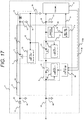
- FIG. 17 is a diagram illustrating a configuration of an electronic control device according to a conventional example.
- a power supply control device 4 includes a first power supply 1, a second power supply 2, and a third power supply 3.
- a battery voltage 41 is input as an input voltage to the power supply control device 4, and the battery voltage 41 is input to the first power supply 1 via a reverse connection prevention diode 42.
- the first power supply 1 is a step-down switching regulator and steps down a first power supply input voltage 44 to a first power supply output voltage 17.
- the first power supply 1 includes a switching element 11, a freewheel diode 15, an inductor 14, and a first voltage control circuit 12.
- the switching element 11 supplies the first power supply input voltage 44 to the inductor 14 and supplies a current to the rear stage of the first power supply 1.
- the switching element 11 does not supply the first power supply input voltage 44 to the inductor 14 side and supplies a current to the rear stage of the first power supply 1 by discharging energy stored in the inductor 14 via the freewheel diode 15.
- a switching output voltage 13 is the first power supply input voltage 44 when the first voltage control circuit 12 instructs turning-on, and is a reference potential 45 when the first voltage control circuit 12 instructs turning-off.
- the first voltage control circuit 12 monitors the first power supply output voltage 17 and controls the switching element 11 in a pulse width modulation (PWM) manner such that the first power supply output voltage 17 is a predetermined voltage.
- PWM pulse width modulation
- the second power supply 2 is a series regulator that supplies a voltage to a microcontroller 5.
- the second power supply 2 includes a second power supply output transistor 21 and a second voltage control circuit 22.
- the second voltage control circuit 22 monitors a second power supply output voltage 24 and controls the second power supply output transistor 21 using the first power supply output voltage 17 as an input voltage such that the second power supply output voltage 24 is a predetermined voltage.
- the third power supply 3 is a series regulator that supplies a voltage to, for example, a sensor outside the electronic control device, other than the microcontroller 5.
- the third power supply 3 includes a third power supply output transistor 31 and a third voltage control circuit 32.
- the third voltage control circuit 32 monitors a third power supply output voltage 34 and controls the third power supply output transistor 31 using the first power supply output voltage 17 as an input voltage such that the third power supply output voltage 34 is a predetermined voltage. In the following description, it is assumed that the third power supply output voltage 34 is controlled to the same voltage as the second power supply output voltage 24.
- the power supply control device 4 includes a voltage generating function control register 36 for the third power supply 3.
- a third power supply output-ON control signal 110a is transmitted to the voltage generating function control register 36 by serial communication or the like, the voltage generating function control register 36 becomes high, the third power supply 3 is turned on, and the third voltage control circuit 32 monitors the third power supply output voltage 34 and controls the third power supply output transistor 31 such that the third power supply output voltage 34 is a predetermined voltage.
- the microcontroller 5 generally has a guaranteed operating range for a source voltage, and when a source voltage outside the guaranteed operating range is supplied, the operation of the microcontroller 5 is not guaranteed. Accordingly, when the source voltage of the microcontroller 5 is outside the guaranteed operating range, a reset signal 71 is output to the microcontroller 5 to prevent an unexpected operation of the microcontroller 5.
- the power supply control device 4 includes a second power supply low output voltage detection circuit 25 for the second power supply output voltage 24.
- the second power supply low output voltage detection circuit 25 detects a low voltage of the second power supply output voltage 24 and outputs a second power supply low output voltage detection output signal 72, and a reset signal generation circuit 71a generates the reset signal 71 and outputs the reset signal 71 to the microcontroller 5 when the second power supply output voltage 24 is continuously in the low-voltage state.
- a suppliable current value that is, a current capacity, is set in circuit configuration for each of the first power supply 1, the second power supply 2, and the third power supply 3.
- a current larger than the current capacity is drawn out from the power supply output, voltage control of stepping down a voltage to a predetermined voltage is not possible and a voltage value lower than a target voltage value is acquired.
- the third power supply 3 supplies a voltage to an ECU-outside sensor, there is a possibility that a signal line of the third power supply output voltage 34 will be grounded. In this case, a third power supply output current is equal to or larger than the current capacity, which causes the above-mentioned phenomenon.
- a first power supply output current is the total sum of the second power supply output current and the third power supply output current.
- the first power supply 1 cannot control the first power supply output voltage 17 to a predetermined voltage value due to an insufficient input voltage on the basis of characteristics of the step-down switching regulator. Since the first power supply output voltage 17 is equal to or lower than the step-down control voltage value of the first power supply 1, the switching element 11 is controlled to be fully turned on to increase the first power supply output voltage 17. At this time, the first power supply output voltage 17 is a voltage which is obtained by subtracting an ON-resistance value of the switching element 11, a series resistance value of the inductor 14, and a voltage drop determined by the first power supply output current value from the first power supply input voltage 44.
- the second power supply 2 uses the first power supply output voltage 17 which is lower than a normal voltage as an input voltage and controls the second power supply output voltage 24 to a predetermined voltage .
- a minimum potential difference (a dropout voltage) between an input and an output is set on the basis of the characteristics of the output transistor. Accordingly, the second power supply output voltage 24 is controlled to a target voltage value when a difference between the first power supply output voltage 17 and a control voltage value of the second power supply 2 is equal to or higher than the dropout voltage, but becomes a voltage obtained by subtracting the dropout voltage from the first power supply output voltage 17 due to an insufficient input voltage when the difference between the first power supply output voltage 17 and the control voltage value of the second power supply 2.
- the third power supply 3 exhibits the same behavior as the second power supply 2, and the third power supply output voltage 34 is controlled to a target voltage value when a difference between the first power supply output voltage 17 and a control voltage value of the third power supply 3 is equal to or higher than the dropout voltage, but becomes a voltage obtained by subtracting the dropout voltage from the first power supply output voltage 17 due to an insufficient input voltage when the difference between the first power supply output voltage 17 and the control voltage value of the third power supply 3.
- the ON-resistance value of the switching element 11 of the first power supply 1, the series resistance value of the inductor 14, the dropout voltage of the second power supply 2, and the dropout voltage of the third power supply 3 in consideration of the above-mentioned details and current consumption of a power supply target at the time of design.
- the ON-resistance value of the switching element 11 of the first power supply 1, the dropout voltage of the second power supply 2, and the dropout voltage of the third power supply 3 greatly depend on the areas of the output transistors used in the power supplies.
- the third power supply 3 supplies a voltage to a sensor outside the electronic control device, there is a possibility that the signal line of the third power supply output voltage 34 will be grounded.
- the third power supply output current becomes larger than the current consumption of the power supply target and increases up to the current capacity of the third power supply 3 in maximum.
- the increase in the third power supply output current is an increase in the first power supply output current.
- a first power supply output current 66 increases with an increase in a third power supply output current 68.
- the first power supply 1 controls the switching element 11 to be fully turned on at a low battery voltage. Accordingly, when the first power supply output voltage 17 decreases with an increase in the first power supply output current 66, the input voltage of the second power supply 2 is insufficient and the second power supply output voltage 24 cannot be controlled with a control voltage 61 for the second power supply. Until the second power supply output voltage 24 is stabilized to a voltage obtained by subtracting the dropout voltage from the first power supply output voltage 17, electric charges accumulated in a second power supply output capacitor 23 supplies current consumption of the microcontroller 5 which is a supply target of the second power supply 2.
- the second power supply low output voltage detection output signal 72 is generated and the reset signal 71 is output to the microcontroller 5 after a reset signal generation filtering time 75. Accordingly, when a ground failure of the third power supply output voltage 34 occurs at a low battery voltage, the battery voltage is within the guaranteed operating range of the electronic control device but the power supply control device 4 stops the operating of the microcontroller 5 and thus there is a problem in that the electronic control device cannot function normally.
- a method of decreasing the ON-resistance value of the switching element 11 of the first power supply 1 and the dropout voltage of the second power supply 2 so as for the power supply control device to control the second power supply output voltage 24 to a target voltage value is used in consideration of a case in which the ground failure of the third power supply output voltage 34 occurs at a low battery voltage.
- this method causes an increase in area of the output transistor which is used in the power supply control device as described above, thereby causing an increase in cost of the power supply control device.
- specifications having excessive characteristics are obtained, thereby interfering with optimization of the function and the cost.
- FIG. 19 is a timing chart in a case in which the battery voltage 41 is disconnected when a ground failure does not occur in the third power supply output voltage 34.
- a power supply control device input capacitor 43 functions as a battery of the power supply control device and the power supply control device operates, but electric charges accumulated in the power supply control device input capacitor 43 decrease with the operation of the power supply control device and thus the first power supply input voltage 44 gradually decreases.
- the second power supply output voltage 24 also decreases with the decrease in the first power supply input voltage 44 and becomes lower than the second power supply low output voltage detection threshold 64, the second power supply low output voltage detection output signal 72 is generated and the reset signal 71 is output to the microcontroller 5 after the reset signal generation filtering time 75.
- the reset signal 71 is output and the operation of the microcontroller 5 is limited to an operation within the guaranteed operating range for the source voltage of the microcontroller 5. Accordingly, the microcontroller 5 operates as designed.
- FIG. 20 is a timing chart in a case in which the battery voltage 41 is disconnected when a ground failure occurs in the third power supply output voltage 34.
- the first power supply output current 66 increases with the increase in the third power supply output current 68.
- a decreasing speed of the first power supply input voltage 44 after the battery voltage 41 is disconnected is higher than that when a ground failure does not occur in the third power supply output voltage 34 and the decreasing speed of the second power supply output voltage 24 also becomes higher.
- the second power supply output voltage 24 is lower than the microcontroller guaranteed operating voltage range lower limit 62, there is a possibility that the reset signal 71 will be output. That is, there is a possibility that the operation of the microcontroller 5 is not limited to an operation within the guaranteed operating range for the source voltage of the microcontroller 5 and thus the microcontroller 5 performs an unexpected operation.
- PTL 2 discloses a power supply apparatus for generating a second voltage to be supplied to a control IC and a third voltage to be supplied to the microcomputer. Said apparatus is also capable of transmitting a reset signal and bypassing the second voltage to an input of the third voltage in a case where the second voltage is reduced.
- PTL 3 discloses another example of power supply control device with a step-down switching regulator using an onboard battery voltage and two series regulators in parallel to supply the core and the I/O of a microcontroller. This device detects a battery voltage decrease and uses a reset control circuit to control the two series regulators.
- An object of the present invention is to provide a power supply system that does not generate a reset signal to a microcontroller even when abnormality occurs in an output of a third power supply within a battery voltage range in which an operation of an electronic control device is guaranteed and to realize the power supply system with a low cost.
- the electronic control device may further include a unit configured to switch the circuit operating state of the third power supply circuit using only a state detection signal generated from the third power supply circuit state.
- the electronic control device even when ground failure occurs in a sensor power supply outside the electronic control device within the battery voltage range in which the operation of the electronic control device is guaranteed, appropriate voltage and current can be continuously supplied to the microcontroller and a reset signal is not output thereto. Accordingly, the electronic control device can function normally.
- FIG. 1 is a diagram illustrating a configuration of an electronic control device according to a first embodiment.
- a third power supply abnormal current detection circuit 35 determines that the third power supply output current is abnormal, and outputs a third power supply abnormal output current detection output signal 73.
- the second power supply low output voltage detection output signal 72 is a signal output when the second power supply low output voltage detection circuit 25 determines that the second power supply output voltage 24 is a low voltage.
- a NAND circuit 51 is a circuit that outputs a negative logical signal using the third power supply abnormal output current detection output signal 73 and the second power supply low output voltage detection output signal 72 as input signals.
- the output signal of the NAND circuit 51 is transmitted to a voltage generating function control register 36 via a filter circuit 52 having a predetermined filtering time.
- the configuration illustrated in FIG. 1 is provided. Accordingly, when the voltage generating function control register 36 is at a high level, that is, the third power supply 3 is turned on, and a low signal is transmitted from the NAND circuit 51 to the voltage generating function control register 36 via the filter circuit 52, the third power supply 3 is turned off by forcibly switching the voltage generating function control register 36 to a low level.
- FIG. 2 is a timing chart illustrating advantages when a ground failure of a third power supply output voltage 34 occurs at a low battery voltage according to the first embodiment.
- the third power supply output current 68 increases when a ground failure occurs in the third power supply output voltage 34, and the third power supply abnormal output current detection output signal 73 is output when the third power supply output current is larger than a third power supply abnormal output current detection threshold 65.
- a first power supply output current 66 increases with the increase in the third power supply output current 68.
- the first power supply 1 controls a switching element 11 in a full turning-on manner. Accordingly, when the first power supply output voltage 17 decreases with the increase in the first power supply output current 66, the input voltage of the second power supply 2 is insufficient and the second power supply output voltage 24 cannot be controlled with a control voltage 61 for the second power supply.
- the second power supply low output voltage detection output signal 72 is generated and the third power supply 3 is turned off in an NAND output signal filtering time 74 after the third power supply abnormal output current detection output signal 73 and the second power supply low output voltage detection output signal 72 are simultaneously output.
- the NAND output signal filtering time 74 is set to be shorter than a reset signal generation filtering time 75.
- the third power supply 3 is controlled as described above to stop the third power supply output current 68 and to decrease the first power supply output current 66. Accordingly, since the first power supply output voltage 17 which is the input voltage of the second power supply 2 increases to a normal range at a low battery voltage and the insufficiency of the input voltage of the second power supply 2 is solved, the second power supply output voltage 24 can be controlled to a predetermined voltage.
- the power supply control device of the electronic control device can maintain supply of appropriate voltage and current to the microcontroller and does not output a reset signal, and thus the electronic control device can function normally.
- FIG. 3 is a timing chart illustrating advantages when the battery voltage 41 is disconnected while a ground failure occurs in the third power supply output voltage 34 in the first embodiment.
- the third power supply output current 68 increases when a ground failure occurs in the third power supply output voltage 34, and the third power supply abnormal output current detection output signal 73 is output when the third power supply output current 68 is larger than the third power supply abnormal output current detection threshold 65.
- the first power supply output current 66 increases with the increase in the third power supply output current 68. With the increase in the first power supply output current 66, the decreasing speed of the first power supply input voltage 44 after the battery voltage 41 is disconnected is higher than that in a case in which a ground failure does not occur in the third power supply output voltage 34 and the decreasing speed of the second power supply output voltage 24 also increases.
- the second power supply low output voltage detection output signal 72 is generated and the third power supply 3 is turned off in the NAND output signal filtering time 74 after the third power supply abnormal output current detection output signal 73 and the second power supply low output voltage detection output signal 72 are simultaneously output.
- the reset sighal 71 can be output when the second power supply output voltage 24 is higher than the microcontroller guaranteed operating voltage range lower limit 62.
- the power supply control device outputs a reset signal within the guaranteed operating range for the source voltage of the microcontroller in the electronic control device according to the present invention and it is thus possible to prevent an unexpected operation of the microcontroller.
- FIG. 4 is a diagram illustrating a configuration of an electronic control device according to a second embodiment.
- the second embodiment is different from the first embodiment, in that a first power supply low output voltage detection circuit 18 is connected to the first power supply output voltage 17 and outputs a first power supply low input voltage detection output signal 76.
- the others are the same as in the first embodiment.
- FIG. 5 illustrates a state in which the third power supply output voltage 34 is grounded when the first power supply input voltage 44 is at a low level.
- the third power supply output current 68 increases as illustrated in FIG. 5 (a short-circuit current flows) .
- the third power supply output voltage 34 reaches the third power supply abnormal output current detection threshold 65, this state is detected and the third power supply abnormal output current detection output signal 73 is output.
- the third power supply output current 68 increases due to the grounding of the third power supply output voltage 34, the first power supply output voltage 17 also decreases similar to the first embodiment.
- the third power supply output current 68 reaches a first power supply low output voltage detection threshold 69 of the first power supply low output voltage detection circuit 18, the first power supply low input voltage detection output signal 76 is output at a first power supply low output voltage detection timing 95.
- the third power supply abnormal output current detection output signal 73 and the first power supply low input voltage detection output signal 76 are simultaneously output, and the third power supply 3 is turned off at a third power supply OFF timing 93 to stop the third power supply output current 68 and to decrease the first power supply output current 66 after the NAND output signal filtering time 74 elapses. Accordingly, since drop of the first power supply output voltage 17 and drop of the second power supply output voltage 24 due to the short-circuit current do not occur as illustrated in FIG. 5 , the second power supply 2 can control the second power supply output voltage 24 to a predetermined voltage. As a result, the reset signal 71 can be kept at a high level.
- the power supply control device of the electronic control device can maintain supply of appropriate voltage and current to the microcontroller and does not output a reset signal, and thus the electronic control device can function normally.
- FIG. 6 is a diagram illustrating a configuration of an electronic control device according to a third embodiment.
- the third embodiment is different from the first and second embodiments, in that a first power supply low input voltage detection circuit 46 is connected to the first power supply input voltage 44 and outputs a first power supply low input voltage detection output signal 77.
- the others are the same as in the first and second embodiments.
- FIG. 7 illustrates a state in which the third power supply output voltage 34 is grounded when the first power supply input voltage 44 is at a low level.
- the decrease of the first power supply input voltage 44 is detected at a first power supply low input voltage detection timing 96 and a first power supply low input voltage detection output signal 77 is output.
- the third power supply output voltage 34 is grounded at the third power supply output ground timing 91, the third power supply output current 68 increases (a short-circuit current flows) as illustrated in FIG. 7 . Then, when the third power supply output voltage 34 reaches the third power supply abnormal output current detection threshold 65, this state is detected and the third power supply abnormal output current detection output signal 73 is output.
- the third power supply abnormal output current detection output signal 73 and the first power supply low input voltage detection output signal 77 are simultaneously output, and the third power supply 3 is turned off at a third power supply OFF timing 93 to stop the third power supply output current 68 and to decrease the first power supply output current 66 after the NAND output signal filtering time 74 elapses. Accordingly, since drop of the first power supply output voltage 17 and drop of the second power supply output voltage 24 due to the short-circuit current do not occur as illustrated in FIG. 7 , the second power supply 2 can control the second power supply output voltage 24 to a predetermined voltage. As a result, the reset signal 71 can be kept at a high level.
- the power supply control device of the electronic control device can maintain supply of appropriate voltage and current to the microcontroller and does not output a reset signal, and thus the electronic control device can function normally.
- FIG. 8 is a diagram illustrating a configuration of an electronic control device according, to a fourth embodiment.
- the fourth embodiment is different from the first to third embodiments, in that a third power supply over-temperature detection circuit 37 is disposed in the vicinity of the third power supply 3 and a third power supply over-temperature detection output signal 81 is output when an abnormal temperature of the third power supply 3 is detected.
- the others are the same as in the first to third embodiments.
- FIG. 9 illustrates a state in which the third power supply output voltage 34 is grounded when the first power supply input voltage 44 is at a low level.
- the third power supply output current 68 increases (the short-circuit current flows) as illustrated in FIG. 9 . Since an amount of heat is generated which is calculated using the third power supply output current 68 flowing at that time and the ON resistance value of the third power supply output transistor 31, a third power supply temperature 83 detected by the third power supply over-temperature detection circuit 37 also increases with the increase of the third power supply output current 68 as illustrated in FIG. 9 .
- the third power supply temperature 83 reaches a third power supply over-temperature detection threshold 82, this state is detected and the third power supply over-temperature detection output signal 81 is output at a third power supply over-temperature detection timing 97.
- the second power supply low output voltage detection output signal 72 is output at a second power supply low output voltage detection timing 92.
- the third power supply over-temperature detection output signal 81 and the second power supply low output voltage detection output signal 72 are simultaneously output, and the third power supply 3 is turned off at the third power supply OFF timing 93 to stop the third power supply output current 68 and to decrease the first power supply output current 66 after the NAND output signal filtering time 74 elapses. Accordingly, since drop of the first power supply output voltage 17 and drop of the second power supply output voltage 24 due to the short-circuit current do not occur as illustrated in FIG. 9 , the second power supply 2 can control the second power supply output voltage 24 to a predetermined voltage. As a result, the reset signal 71 can be kept at a high level.
- the power supply control device of the electronic control device can maintain supply of appropriate voltage and current to the microcontroller and does not output a reset signal, and thus the electronic control device can function normally.
- FIG. 10 is a diagram illustrating a configuration of an electronic control device according to a fifth embodiment.
- the fifth embodiment employs a configuration in which the third power supply abnormal output current detection output signal 73 detected by the third power supply abnormal current detection circuit 35 is input to a filter circuit 52 via an inverter circuit 53.
- a third power supply output-ON control signal 110a is input to the voltage generating function control register 36.
- the power supply output-ON control signal is a register setting signal and is generally input from an external control device such as a CPU.
- FIG. 11 illustrates a state in which the third power supply output voltage 34 is grounded when the first power supply input voltage 44 is at a low level.
- the third power supply output current 68 increases (the short-circuit current flows) as illustrated in FIG. 11 .
- the third power supply output current 68 reaches the third power supply abnormal output current detection threshold 65, this state is detected and the third power supply abnormal output current detection output signal 73 is output.
- the third power supply abnormal output current detection output signal 73 is output, and the third power supply 3 is turned off at the third power supply OFF timing 93 after the inverter output signal filtering time 78 by the filter circuit 52 elapses to stop the third power supply output current 68 and to decrease the first power supply output current 66. Accordingly, since drop of the first power supply output voltage 17 and drop of the second power supply output voltage 24 due to the short-circuit current do not occur as illustrated in FIG. 11 , the second power supply 2 can control the second power supply output voltage 24 to a predetermined voltage. As a result, the reset signal 71 can be kept at a high level.
- the power supply control device of the electronic control device can maintain supply of appropriate voltage and current to the microcontroller and does not output a reset signal, and thus the electronic control device can function normally.
- the fifth embodiment provides the following advantages.
- the third power supply 3 is turned off using the third power supply abnormal output current detection output signal 73. Accordingly, when the power supply is turned off, the current value is zero and thus the third power supply abnormal output current detection output signal 73 is returned to a normal state. Then, since the operation of controlling the third power supply 3 to be turned on again and to allow the short-circuit current to flow and outputting the third power supply abnormal output current detection output signal 73 again to turn off the third power supply 3 is repeated, this operation is repeated until the short-circuit state of the third power supply 3 is released.
- the third power supply output-ON control signal 110a is input to the voltage generating function control register 36. Accordingly, when the third power supply 3 is once turned off using the third power supply abnormal output current detection output signal 73 and then the third power supply 3 is turned on, the third power supply output-ON control signal 110a is input to turn on the third power supply 3 again as indicated by a third power supply ON timing 99 in FIG. 11 . Accordingly, it is possible to avoid the operation of repeating the ON state and the OFF state until the short-circuit state of the third power supply 3 is released as described above.
- FIG. 12 is a diagram illustrating a configuration of an electronic control device according to a sixth embodiment.
- the sixth embodiment is different from the first to fifth embodiments, in that a first power supply input and output voltage difference detection circuit 111 configured to compare the first power supply input voltage 44 and the first power supply output voltage 17 is provided and outputs a first power supply input and output voltage difference detection signal 112. At this time, in order to detect that the first power supply 1 is in a fully turned-on state, the driving signal of the switching element 11 is also input to the first power supply input and output voltage difference detection circuit 111.
- the others are the same as in the first to fifth embodiments.
- FIG. 13 illustrates a state in which the third power supply output voltage 34 is grounded when the first power supply input voltage 44 is at a low level.
- the third power supply output current 68 increases (the short-circuit current flows) as illustrated in FIG. 13 .
- the third power supply output current 68 reaches the third power supply abnormal output current detection threshold 65, this state is detected and the third power supply abnormal output current detection output signal 73 is output.
- the first power supply output voltage 17 is input to the first power supply input and output voltage difference detection circuit 111, and when the first power supply output voltage 17 reaches a first power supply input and output voltage difference detection threshold 114 set in the first power supply input and output voltage difference detection circuit 111, the first power supply input and output voltage difference detection signal 112 is output at a first power supply input and output voltage difference detection timing 100.
- the potential difference is detected using the driving signal of the switching element 11 only when the switching element 11 is fully turned on.
- the third power supply abnormal output current detection output signal 73 and the first power supply input and output voltage difference detection signal 112 are simultaneously output, and the third power supply 3 is turned off at the third power supply OFF timing 93 to stop the third power supply output current 68 and to decrease the first power supply output current 66 after the NAND output signal filtering time 74 elapses . Accordingly, since drop of the first power supply output voltage 17 and drop of the second power supply output voltage 24 due to the short-circuit current do not occur as illustrated in FIG. 13 , the second power supply 2 can control the second power supply output voltage 24 to a predetermined voltage. As a result, the reset signal 71 can be kept at a high level.
- the power supply control device of the electronic control device can maintain supply of appropriate voltage and current to the microcontroller and does not output a reset signal, and thus the electronic control device can function normally.
- FIG. 14 is a diagram illustrating a configuration of an electronic control device according to a seventh embodiment.
- the seventh embodiment is different from the first to sixth embodiments, in that a second power supply input and output voltage difference detection circuit 115 configured to compare the second power supply output voltage 24 with the first power supply output voltage 17 which is the second power supply input voltage is provided and outputs a second power supply input and output voltage difference detection signal 116.
- the others are the same as in the first to sixth embodiments.
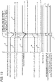
- FIG. 15 illustrates a state in which the third power supply output voltage 34 is grounded when the first power supply input voltage 44 is at a low level.
- the third power supply output current 68 increases (the short-circuit current flows) as illustrated in FIG. 15 .
- the third power supply output current 68 reaches the third power supply abnormal output current detection threshold 65, this state is detected and the third power supply abnormal output current detection output signal 73 is output.
- the first power supply output voltage 17 and the second power supply output voltage 24 also decrease similar to the first embodiment.
- These voltages are input to the second power supply input and output voltage difference detection circuit 115, and when the voltages reach a second power supply input and output voltage difference detection threshold 118 set in the second power supply input and output voltage difference detection circuit 115, the first power supply input and output voltage difference detection signal 116 is output at a second power supply input and output voltage difference detection timing 101.
- the third power supply abnormal output current detection output signal 73 and the second power supply input and output voltage difference detection signal 116 are simultaneously output, and the third power supply 3 is turned off at the third power supply OFF timing 93 to stop the third power supply output current 68 and to decrease the first power supply output current 66 after the NAND output signal filtering time 74 elapses. Accordingly, since drop of the first power supply output voltage 17 and drop of the second power supply output voltage 24 due to the short-circuit current do not occur as illustrated in FIG. 15 , the second power supply 2 can control the second power supply output voltage 24 to a predetermined voltage. As a result, the reset signal 71 can be kept at a high level.
- the electronic control device can maintain supply of appropriate voltage and current to the microcontroller and does not output a reset signal, and thus the electronic control device can function normally.
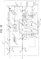
- FIG. 16 is a diagram illustrating a configuration of an electronic control device according to an eighth embodiment.
- the eighth embodiment employs a configuration in which first power supply low input voltage detection output signal 77 detected by the first power supply low input voltage detection circuit 46 is input to the filter circuit 52 via the inverter circuit 53.
- the others are the same as in the first to seventh embodiments.
- the power supply control device starts control of the power supplies in response to a power supply control device permission signal which is not illustrated.
- the first power supply 1 first starts its operation and the second power supply 2 and the third power supply 3 start their operations when the first power supply output voltage 17 reaches a predetermined voltage. That is, regarding the third power supply 3, when the power supply control device is started, the voltage generating function control register 36 is automatically set to a high level and the third power supply 3 starts its operation.
- the first power supply input voltage 44 is at a low level when the power supply control device is started.
- the voltage generating function control register 36 is automatically set to a high level, the first power supply output voltage 17 decreases with the increase of the third power supply output current 68 and the second power supply input voltage is insufficient. Accordingly, there is a possibility that the second power supply output voltage 24 is not higher than the second power supply low output voltage detection threshold 64 and the reset signal 71 is in a high state.
- the power supply control device is started in a state in which the third power supply output voltage 34 is grounded, the third power supply output current 68 is larger than current consumption of the power supply target and thus the above-mentioned possibility increases.
- the first power supply low input voltage detection output signal 77 is input to the voltage generating function control register 36 via the inverter circuit 53 and the filter circuit 52.
- the first power supply low input voltage detection circuit 46 detects that the first power supply input voltage 44 is at a low level and outputs the first power supply low input voltage detection output signal 77, thereby preventing the voltage generating function control register 36 from being automatically set to a high level.
Landscapes
- Engineering & Computer Science (AREA)
- Power Engineering (AREA)
- Mechanical Engineering (AREA)
- Life Sciences & Earth Sciences (AREA)
- Sustainable Development (AREA)
- Sustainable Energy (AREA)
- Transportation (AREA)
- Physics & Mathematics (AREA)
- General Physics & Mathematics (AREA)
- Automation & Control Theory (AREA)
- General Engineering & Computer Science (AREA)
- Electromagnetism (AREA)
- Radar, Positioning & Navigation (AREA)
- Continuous-Control Power Sources That Use Transistors (AREA)
- Dc-Dc Converters (AREA)
- Direct Current Feeding And Distribution (AREA)
- Electronic Switches (AREA)
- Charge And Discharge Circuits For Batteries Or The Like (AREA)
Claims (8)
- Dispositif de commande électronique (6) comprenant :- un microcontrôleur (5) ;- un premier circuit d'alimentation de puissance (1), étant un régulateur de commutation d'abaissement, qui utilise une tension de batterie embarquée (41) à titre de tension d'entrée et qui sort une tension prédéterminée (17) ;- un deuxième circuit d'alimentation de puissance (2), étant un régulateur en série, qui utilise la première tension de sortie d'alimentation de puissance (17) provenant du premier circuit d'alimentation de puissance (1) à titre de tension d'entrée et qui sort une tension prédéterminée (24) vers le microcontrôleur (5) ; et- un troisième circuit d'alimentation de puissance (3), étant un régulateur en série, qui utilise la première tension de sortie d'alimentation de puissance (17) provenant du premier circuit d'alimentation de puissance (1) à titre de tension d'entrée et qui sort une tension prédéterminée (34) vers l'extérieur du dispositif de commande (6), dans lequel un état de fonctionnement de circuit du troisième circuit d'alimentation de puissance (3) est commuté en dépendance d'un état du premier circuit d'alimentation de puissance (1), du deuxième circuit d'alimentation de puissance (2) ou du troisième circuit d'alimentation de puissance (3), dans lequel l'unité (35) qui détecte l'état du troisième circuit d'alimentation de puissance (3) est configurée pour surveiller un courant de sortie (68) du troisième circuit d'alimentation de puissance (3), et pour générer un signal de détection de courant anormal du troisième circuit d'alimentation de puissance (3) sur la base du courant de sortie en augmentation (68) du troisième circuit d'alimentation de puissance (3), quand une défaillance de terre survient dans la troisième tension de sortie d'alimentation de puissance (34), pour désactiver le troisième circuit d'alimentation de puissance (3) et pour empêcher une génération de signal de réinitialisation inattendue vers un microcontrôleur.
- Dispositif de commande électronique (6) selon la revendication 1, comprenant en outre :- une unité configurée pour générer un signal de détection d'état sur la base de l'état du troisième circuit d'alimentation de puissance (3), dans lequell'état de fonctionnement de circuit du troisième circuit d'alimentation de puissance (3) est commuté sur la base du signal de détection d'état.
- Dispositif de commande électronique (6) selon la revendication 1, comprenant en outre :- une unité (25) configurée pour générer un signal de détection de tension pour au moins une tension parmi des tensions d'entrée et des tensions de sortie du premier, du deuxième et du troisième circuit d'alimentation de puissance, dans lequell'état de fonctionnement de circuit du troisième circuit d'alimentation de puissance (3) est commuté sur la base du signal de détection d'état et du signal de détection de tension.
- Dispositif de commande électronique (6) selon la revendication 1, dans lequel
l'unité (25) qui détecte la tension est configurée pour surveiller au moins une des tensions de sortie d'alimentation de puissance du premier et du deuxième circuit d'alimentation, et pour générer un premier ou un second signal de détection de tension de sortie bas d'alimentation de puissance sur la base de la tension de sortie de la première ou de la seconde tension de sortie d'alimentation de puissance. - Dispositif de commande électronique (6) selon la revendication 1, dans lequel
l'unité (25) qui détecte la tension est configurée pour surveiller une première tension d'entrée d'alimentation de puissance ; et pour générer un premier signal de détection de tension d'entrée bas d'alimentation de puissance sur la base de la première tension d'entrée d'alimentation de puissance. - Dispositif de commande électronique (6) selon la revendication 1, comprenant en outre :- une unité configurée pour commuter un état de démarrage de circuit du troisième circuit d'alimentation de puissance (3) en dépendance d'états de tensions d'entrée ou de tensions de sortie après que le premier, le deuxième et le troisième circuit d'alimentation de puissance ont démarré leur fonctionnement.
- Dispositif de commande électronique (6) selon la revendication 1, dans lequel
le troisième circuit d'alimentation de puissance (3) inclut une unité (32) configurée pour commander l'état de fonctionnement de circuit d'un transistor de sortie de troisième alimentation de puissance (31). - Dispositif de commande électronique (6) selon la revendication 1, comprenant en outre :- un microcontrôleur (5) configuré pour exécuter des fonctionnements variés ; et- une unité configurée pour surveiller une deuxième tension de sortie d'alimentation de puissance (24) et pour sortir un signal d'initialisation vers le microcontrôleur (5) quand la deuxième tension de sortie d'alimentation de puissance (24) est plus basse qu'une tension prédéterminée (17).
Applications Claiming Priority (2)
| Application Number | Priority Date | Filing Date | Title |
|---|---|---|---|
| JP2014119249 | 2014-06-10 | ||
| PCT/JP2015/066431 WO2015190421A1 (fr) | 2014-06-10 | 2015-06-08 | Dispositif de commande électronique |
Publications (3)
| Publication Number | Publication Date |
|---|---|
| EP3157151A1 EP3157151A1 (fr) | 2017-04-19 |
| EP3157151A4 EP3157151A4 (fr) | 2018-04-11 |
| EP3157151B1 true EP3157151B1 (fr) | 2021-08-11 |
Family
ID=54833513
Family Applications (1)
| Application Number | Title | Priority Date | Filing Date |
|---|---|---|---|
| EP15807336.1A Active EP3157151B1 (fr) | 2014-06-10 | 2015-06-08 | Dispositif de commande électronique |
Country Status (5)
| Country | Link |
|---|---|
| US (1) | US10525913B2 (fr) |
| EP (1) | EP3157151B1 (fr) |
| JP (1) | JP6232133B2 (fr) |
| CN (1) | CN106464138B (fr) |
| WO (1) | WO2015190421A1 (fr) |
Families Citing this family (4)
| Publication number | Priority date | Publication date | Assignee | Title |
|---|---|---|---|---|
| JP6539201B2 (ja) * | 2015-12-25 | 2019-07-03 | 日立オートモティブシステムズ株式会社 | スイッチング電源、電源回路及び車載制御装置 |
| US20170357282A1 (en) * | 2016-06-08 | 2017-12-14 | Integrated Device Technology, Inc. | Autonomous power and timing system |
| CN109752985A (zh) * | 2017-11-08 | 2019-05-14 | 上海海拉电子有限公司 | 一种车载开关控制系统及具有该系统的车辆 |
| JP7024519B2 (ja) * | 2018-03-14 | 2022-02-24 | カシオ計算機株式会社 | 電源装置、電子機器及び電源装置の制御方法 |
Family Cites Families (30)
| Publication number | Priority date | Publication date | Assignee | Title |
|---|---|---|---|---|
| JPH05127765A (ja) * | 1991-11-01 | 1993-05-25 | Nippondenso Co Ltd | 車載用電子装置の電源装置 |
| JPH11265225A (ja) | 1998-03-16 | 1999-09-28 | Toyota Motor Corp | エンジン制御装置用の電源装置 |
| US6304089B1 (en) * | 1998-10-26 | 2001-10-16 | Garry E. Paulson | Parallel termination apparatus and method for ground-check monitors |
| US7173275B2 (en) * | 2001-05-21 | 2007-02-06 | Regents Of The University Of Colorado | Thin-film transistors based on tunneling structures and applications |
| JP2003092874A (ja) | 2001-09-18 | 2003-03-28 | Hitachi Unisia Automotive Ltd | 車両用電源装置 |
| CA2422307A1 (fr) * | 2002-03-20 | 2003-09-20 | Stefanie Livanos | Dispositif de prelevement sanguin |
| JP3705259B2 (ja) | 2002-10-22 | 2005-10-12 | 株式会社デンソー | 電源コントローラ |
| JP4107052B2 (ja) * | 2002-10-30 | 2008-06-25 | 株式会社デンソー | 多出力電源装置 |
| US7187529B2 (en) * | 2003-04-30 | 2007-03-06 | Eaton Corporation | Apparatus and method for detecting a gas associated with a glowing contact and interrupting a power circuit |
| US7275589B2 (en) * | 2004-03-17 | 2007-10-02 | The Babcock & Wilcox Company | Anti-vibration bars for boiler tubes with protective shields |
| JP4683950B2 (ja) * | 2004-05-11 | 2011-05-18 | 株式会社リコー | スイッチ装置及び電気機器 |
| JP4523330B2 (ja) * | 2004-05-11 | 2010-08-11 | 株式会社リコー | 電源回路及びその電源回路を有する機器 |
| JP4476730B2 (ja) * | 2004-07-28 | 2010-06-09 | 三菱電機株式会社 | 放電灯点灯装置 |
| JP4254703B2 (ja) * | 2004-12-07 | 2009-04-15 | 株式会社デンソー | 誘導性負荷駆動装置 |
| JP4212560B2 (ja) * | 2005-01-21 | 2009-01-21 | パナソニック株式会社 | 電源回路 |
| CN100469053C (zh) * | 2005-06-29 | 2009-03-11 | 株式会社Ntt都科摩 | 通信终端及通信方法 |
| JP4652936B2 (ja) * | 2005-09-09 | 2011-03-16 | 日立プラズマディスプレイ株式会社 | プラズマディスプレイ装置及びその駆動方法 |
| JP4788420B2 (ja) * | 2006-03-17 | 2011-10-05 | 株式会社デンソー | 電源装置 |
| JP4897877B2 (ja) * | 2006-05-10 | 2012-03-14 | クゥアルコム・インコーポレイテッド | 集積回路の電力分配制御の方法及びシステム |
| JP2008046720A (ja) * | 2006-08-11 | 2008-02-28 | Fujitsu Ten Ltd | 電源回路内蔵集積回路、及び、電源回路内蔵集積回路を搭載したオーディオ装置、並びに、電子機器 |
| JP5098367B2 (ja) * | 2007-03-06 | 2012-12-12 | 富士通セミコンダクター株式会社 | 電源電圧調整回路およびマイクロコンピュータ |
| JP2008232871A (ja) * | 2007-03-22 | 2008-10-02 | Hitachi Ltd | 回路異常判定装置および回路異常判定方法 |
| JP4345845B2 (ja) * | 2007-05-16 | 2009-10-14 | 株式会社デンソー | 電源装置 |
| JP4479797B2 (ja) * | 2008-01-23 | 2010-06-09 | 株式会社デンソー | 電子制御装置 |
| US7544077B1 (en) * | 2008-02-08 | 2009-06-09 | Tyco Electronics Corporation | Control device for a power distribution system |
| JP4591571B2 (ja) * | 2008-08-04 | 2010-12-01 | 株式会社デンソー | 電源装置 |
| JP5212016B2 (ja) * | 2008-10-28 | 2013-06-19 | 富士電機株式会社 | スイッチング電源制御回路 |
| JP5368508B2 (ja) | 2011-05-16 | 2013-12-18 | 三菱電機株式会社 | 車載電子制御装置 |
| JP5944172B2 (ja) * | 2012-01-31 | 2016-07-05 | 富士通テン株式会社 | 電源回路 |
| JP5820779B2 (ja) * | 2012-07-06 | 2015-11-24 | 日立オートモティブシステムズ株式会社 | 車載用電源装置 |
-
2015
- 2015-06-08 EP EP15807336.1A patent/EP3157151B1/fr active Active
- 2015-06-08 CN CN201580028263.6A patent/CN106464138B/zh active Active
- 2015-06-08 WO PCT/JP2015/066431 patent/WO2015190421A1/fr not_active Ceased
- 2015-06-08 US US15/315,080 patent/US10525913B2/en active Active
- 2015-06-08 JP JP2016527786A patent/JP6232133B2/ja active Active
Also Published As
| Publication number | Publication date |
|---|---|
| WO2015190421A1 (fr) | 2015-12-17 |
| EP3157151A1 (fr) | 2017-04-19 |
| JP6232133B2 (ja) | 2017-11-15 |
| US10525913B2 (en) | 2020-01-07 |
| EP3157151A4 (fr) | 2018-04-11 |
| JPWO2015190421A1 (ja) | 2017-04-20 |
| US20170190307A1 (en) | 2017-07-06 |
| CN106464138B (zh) | 2019-03-15 |
| CN106464138A (zh) | 2017-02-22 |
Similar Documents
| Publication | Publication Date | Title |
|---|---|---|
| CN101335449B (zh) | 电源保护装置及电子控制装置 | |
| CN101395789B (zh) | 电源系统及其方法 | |
| CN105899406B (zh) | 用于控制车辆电网中多个电网之间电功率切换的控制单元及具有该控制单元的车用电网 | |
| CN107078682B (zh) | 电动机控制装置以及搭载了该电动机控制装置的电动助力转向装置和车辆 | |
| US10065521B2 (en) | System and method for using solar power to supplement power in a DC electrical system | |
| JP2009177909A (ja) | 電子制御装置及び電源装置 | |
| US9669779B2 (en) | Method for operating a multi-voltage electrical system of a motor vehicle, a multi-voltage electrical system and means for implementing the method | |
| US9694692B2 (en) | Vehicle controlling system | |
| CN103532118A (zh) | 涌入电流限制电路 | |
| EP3157151B1 (fr) | Dispositif de commande électronique | |
| JP6308092B2 (ja) | 電子制御装置 | |
| JP2008511277A (ja) | 過電圧保護を行う電圧制御器 | |
| JP2014107989A (ja) | Dc−dcコンバータ | |
| CN107662562A (zh) | 包括转换器和高负载用电器的机动车辆车载电气系统 | |
| US20140266013A1 (en) | Switched voltage booster | |
| JP2009142089A (ja) | 車両用電源装置 | |
| KR20150005868A (ko) | 연료전지차량의 회생제동시스템 및 그 제어방법 | |
| JP7689474B2 (ja) | 制御装置および制御方法 | |
| CN118020224A (zh) | 车载用控制装置 | |
| US11299115B2 (en) | Power storage unit control device | |
| EP3820007B1 (fr) | Dispositif et procédé de protection contre les surtensions | |
| US10479299B2 (en) | Method for controlling a consumer of a low-voltage on-board electrical system | |
| JP2016146699A (ja) | 電源装置 | |
| JP2017017925A (ja) | モータ駆動装置 | |
| US20190351851A1 (en) | Onboard control device and onboard power supply device |
Legal Events
| Date | Code | Title | Description |
|---|---|---|---|
| STAA | Information on the status of an ep patent application or granted ep patent |
Free format text: STATUS: THE INTERNATIONAL PUBLICATION HAS BEEN MADE |
|
| PUAI | Public reference made under article 153(3) epc to a published international application that has entered the european phase |
Free format text: ORIGINAL CODE: 0009012 |
|
| STAA | Information on the status of an ep patent application or granted ep patent |
Free format text: STATUS: REQUEST FOR EXAMINATION WAS MADE |
|
| 17P | Request for examination filed |
Effective date: 20170110 |
|
| AK | Designated contracting states |
Kind code of ref document: A1 Designated state(s): AL AT BE BG CH CY CZ DE DK EE ES FI FR GB GR HR HU IE IS IT LI LT LU LV MC MK MT NL NO PL PT RO RS SE SI SK SM TR |
|
| AX | Request for extension of the european patent |
Extension state: BA ME |
|
| DAV | Request for validation of the european patent (deleted) | ||
| DAX | Request for extension of the european patent (deleted) | ||
| A4 | Supplementary search report drawn up and despatched |
Effective date: 20180314 |
|
| RIC1 | Information provided on ipc code assigned before grant |
Ipc: H02M 3/158 20060101ALI20180308BHEP Ipc: G05B 15/02 20060101ALI20180308BHEP Ipc: H02M 3/155 20060101AFI20180308BHEP Ipc: G05F 1/56 20060101ALI20180308BHEP Ipc: B60L 3/04 20060101ALI20180308BHEP Ipc: H02P 1/16 20060101ALI20180308BHEP Ipc: B60R 16/033 20060101ALI20180308BHEP Ipc: H02M 1/32 20070101ALI20180308BHEP |
|
| STAA | Information on the status of an ep patent application or granted ep patent |
Free format text: STATUS: EXAMINATION IS IN PROGRESS |
|
| 17Q | First examination report despatched |
Effective date: 20201208 |
|
| GRAP | Despatch of communication of intention to grant a patent |
Free format text: ORIGINAL CODE: EPIDOSNIGR1 |
|
| STAA | Information on the status of an ep patent application or granted ep patent |
Free format text: STATUS: GRANT OF PATENT IS INTENDED |
|
| RIC1 | Information provided on ipc code assigned before grant |
Ipc: B60R 16/033 20060101ALI20210331BHEP Ipc: H02M 1/32 20070101ALI20210331BHEP Ipc: H02M 3/158 20060101ALI20210331BHEP Ipc: B60L 3/00 20190101ALI20210331BHEP Ipc: B60L 3/04 20060101ALI20210331BHEP Ipc: H02M 3/155 20060101AFI20210331BHEP |
|
| INTG | Intention to grant announced |
Effective date: 20210419 |
|
| GRAS | Grant fee paid |
Free format text: ORIGINAL CODE: EPIDOSNIGR3 |
|
| GRAA | (expected) grant |
Free format text: ORIGINAL CODE: 0009210 |
|
| STAA | Information on the status of an ep patent application or granted ep patent |
Free format text: STATUS: THE PATENT HAS BEEN GRANTED |
|
| AK | Designated contracting states |
Kind code of ref document: B1 Designated state(s): AL AT BE BG CH CY CZ DE DK EE ES FI FR GB GR HR HU IE IS IT LI LT LU LV MC MK MT NL NO PL PT RO RS SE SI SK SM TR |
|
| REG | Reference to a national code |
Ref country code: CH Ref legal event code: EP |
|
| REG | Reference to a national code |
Ref country code: DE Ref legal event code: R096 Ref document number: 602015072235 Country of ref document: DE |
|
| REG | Reference to a national code |
Ref country code: AT Ref legal event code: REF Ref document number: 1420414 Country of ref document: AT Kind code of ref document: T Effective date: 20210915 Ref country code: IE Ref legal event code: FG4D |
|
| RAP4 | Party data changed (patent owner data changed or rights of a patent transferred) |
Owner name: HITACHI ASTEMO, LTD. |
|
| REG | Reference to a national code |
Ref country code: DE Ref legal event code: R081 Ref document number: 602015072235 Country of ref document: DE Owner name: HITACHI ASTEMO, LTD., HITACHINAKA-SHI, JP Free format text: FORMER OWNER: HITACHI AUTOMOTIVE SYSTEMS, LTD., HITACHINAKA-SHI, IBARAKI, JP |
|
| REG | Reference to a national code |
Ref country code: LT Ref legal event code: MG9D |
|
| REG | Reference to a national code |
Ref country code: NL Ref legal event code: MP Effective date: 20210811 |
|
| REG | Reference to a national code |
Ref country code: AT Ref legal event code: MK05 Ref document number: 1420414 Country of ref document: AT Kind code of ref document: T Effective date: 20210811 |
|
| PG25 | Lapsed in a contracting state [announced via postgrant information from national office to epo] |
Ref country code: SE Free format text: LAPSE BECAUSE OF FAILURE TO SUBMIT A TRANSLATION OF THE DESCRIPTION OR TO PAY THE FEE WITHIN THE PRESCRIBED TIME-LIMIT Effective date: 20210811 Ref country code: RS Free format text: LAPSE BECAUSE OF FAILURE TO SUBMIT A TRANSLATION OF THE DESCRIPTION OR TO PAY THE FEE WITHIN THE PRESCRIBED TIME-LIMIT Effective date: 20210811 Ref country code: HR Free format text: LAPSE BECAUSE OF FAILURE TO SUBMIT A TRANSLATION OF THE DESCRIPTION OR TO PAY THE FEE WITHIN THE PRESCRIBED TIME-LIMIT Effective date: 20210811 Ref country code: NO Free format text: LAPSE BECAUSE OF FAILURE TO SUBMIT A TRANSLATION OF THE DESCRIPTION OR TO PAY THE FEE WITHIN THE PRESCRIBED TIME-LIMIT Effective date: 20211111 Ref country code: PT Free format text: LAPSE BECAUSE OF FAILURE TO SUBMIT A TRANSLATION OF THE DESCRIPTION OR TO PAY THE FEE WITHIN THE PRESCRIBED TIME-LIMIT Effective date: 20211213 Ref country code: ES Free format text: LAPSE BECAUSE OF FAILURE TO SUBMIT A TRANSLATION OF THE DESCRIPTION OR TO PAY THE FEE WITHIN THE PRESCRIBED TIME-LIMIT Effective date: 20210811 Ref country code: FI Free format text: LAPSE BECAUSE OF FAILURE TO SUBMIT A TRANSLATION OF THE DESCRIPTION OR TO PAY THE FEE WITHIN THE PRESCRIBED TIME-LIMIT Effective date: 20210811 Ref country code: AT Free format text: LAPSE BECAUSE OF FAILURE TO SUBMIT A TRANSLATION OF THE DESCRIPTION OR TO PAY THE FEE WITHIN THE PRESCRIBED TIME-LIMIT Effective date: 20210811 Ref country code: BG Free format text: LAPSE BECAUSE OF FAILURE TO SUBMIT A TRANSLATION OF THE DESCRIPTION OR TO PAY THE FEE WITHIN THE PRESCRIBED TIME-LIMIT Effective date: 20211111 Ref country code: LT Free format text: LAPSE BECAUSE OF FAILURE TO SUBMIT A TRANSLATION OF THE DESCRIPTION OR TO PAY THE FEE WITHIN THE PRESCRIBED TIME-LIMIT Effective date: 20210811 |
|
| PG25 | Lapsed in a contracting state [announced via postgrant information from national office to epo] |
Ref country code: PL Free format text: LAPSE BECAUSE OF FAILURE TO SUBMIT A TRANSLATION OF THE DESCRIPTION OR TO PAY THE FEE WITHIN THE PRESCRIBED TIME-LIMIT Effective date: 20210811 Ref country code: LV Free format text: LAPSE BECAUSE OF FAILURE TO SUBMIT A TRANSLATION OF THE DESCRIPTION OR TO PAY THE FEE WITHIN THE PRESCRIBED TIME-LIMIT Effective date: 20210811 Ref country code: GR Free format text: LAPSE BECAUSE OF FAILURE TO SUBMIT A TRANSLATION OF THE DESCRIPTION OR TO PAY THE FEE WITHIN THE PRESCRIBED TIME-LIMIT Effective date: 20211112 |
|
| PG25 | Lapsed in a contracting state [announced via postgrant information from national office to epo] |
Ref country code: NL Free format text: LAPSE BECAUSE OF FAILURE TO SUBMIT A TRANSLATION OF THE DESCRIPTION OR TO PAY THE FEE WITHIN THE PRESCRIBED TIME-LIMIT Effective date: 20210811 |
|
| PG25 | Lapsed in a contracting state [announced via postgrant information from national office to epo] |
Ref country code: DK Free format text: LAPSE BECAUSE OF FAILURE TO SUBMIT A TRANSLATION OF THE DESCRIPTION OR TO PAY THE FEE WITHIN THE PRESCRIBED TIME-LIMIT Effective date: 20210811 |
|
| REG | Reference to a national code |
Ref country code: DE Ref legal event code: R097 Ref document number: 602015072235 Country of ref document: DE |
|
| PG25 | Lapsed in a contracting state [announced via postgrant information from national office to epo] |
Ref country code: SM Free format text: LAPSE BECAUSE OF FAILURE TO SUBMIT A TRANSLATION OF THE DESCRIPTION OR TO PAY THE FEE WITHIN THE PRESCRIBED TIME-LIMIT Effective date: 20210811 Ref country code: SK Free format text: LAPSE BECAUSE OF FAILURE TO SUBMIT A TRANSLATION OF THE DESCRIPTION OR TO PAY THE FEE WITHIN THE PRESCRIBED TIME-LIMIT Effective date: 20210811 Ref country code: RO Free format text: LAPSE BECAUSE OF FAILURE TO SUBMIT A TRANSLATION OF THE DESCRIPTION OR TO PAY THE FEE WITHIN THE PRESCRIBED TIME-LIMIT Effective date: 20210811 Ref country code: EE Free format text: LAPSE BECAUSE OF FAILURE TO SUBMIT A TRANSLATION OF THE DESCRIPTION OR TO PAY THE FEE WITHIN THE PRESCRIBED TIME-LIMIT Effective date: 20210811 Ref country code: CZ Free format text: LAPSE BECAUSE OF FAILURE TO SUBMIT A TRANSLATION OF THE DESCRIPTION OR TO PAY THE FEE WITHIN THE PRESCRIBED TIME-LIMIT Effective date: 20210811 Ref country code: AL Free format text: LAPSE BECAUSE OF FAILURE TO SUBMIT A TRANSLATION OF THE DESCRIPTION OR TO PAY THE FEE WITHIN THE PRESCRIBED TIME-LIMIT Effective date: 20210811 |
|
| PLBE | No opposition filed within time limit |
Free format text: ORIGINAL CODE: 0009261 |
|
| STAA | Information on the status of an ep patent application or granted ep patent |
Free format text: STATUS: NO OPPOSITION FILED WITHIN TIME LIMIT |
|
| 26N | No opposition filed |
Effective date: 20220512 |
|
| PG25 | Lapsed in a contracting state [announced via postgrant information from national office to epo] |
Ref country code: IT Free format text: LAPSE BECAUSE OF FAILURE TO SUBMIT A TRANSLATION OF THE DESCRIPTION OR TO PAY THE FEE WITHIN THE PRESCRIBED TIME-LIMIT Effective date: 20210811 |
|
| PG25 | Lapsed in a contracting state [announced via postgrant information from national office to epo] |
Ref country code: SI Free format text: LAPSE BECAUSE OF FAILURE TO SUBMIT A TRANSLATION OF THE DESCRIPTION OR TO PAY THE FEE WITHIN THE PRESCRIBED TIME-LIMIT Effective date: 20210811 |
|
| PG25 | Lapsed in a contracting state [announced via postgrant information from national office to epo] |
Ref country code: MC Free format text: LAPSE BECAUSE OF FAILURE TO SUBMIT A TRANSLATION OF THE DESCRIPTION OR TO PAY THE FEE WITHIN THE PRESCRIBED TIME-LIMIT Effective date: 20210811 |
|
| REG | Reference to a national code |
Ref country code: CH Ref legal event code: PL |
|
| REG | Reference to a national code |
Ref country code: BE Ref legal event code: MM Effective date: 20220630 |
|
| GBPC | Gb: european patent ceased through non-payment of renewal fee |
Effective date: 20220608 |
|
| PG25 | Lapsed in a contracting state [announced via postgrant information from national office to epo] |
Ref country code: LU Free format text: LAPSE BECAUSE OF NON-PAYMENT OF DUE FEES Effective date: 20220608 Ref country code: LI Free format text: LAPSE BECAUSE OF NON-PAYMENT OF DUE FEES Effective date: 20220630 Ref country code: IE Free format text: LAPSE BECAUSE OF NON-PAYMENT OF DUE FEES Effective date: 20220608 Ref country code: FR Free format text: LAPSE BECAUSE OF NON-PAYMENT OF DUE FEES Effective date: 20220630 Ref country code: CH Free format text: LAPSE BECAUSE OF NON-PAYMENT OF DUE FEES Effective date: 20220630 |
|
| PG25 | Lapsed in a contracting state [announced via postgrant information from national office to epo] |
Ref country code: GB Free format text: LAPSE BECAUSE OF NON-PAYMENT OF DUE FEES Effective date: 20220608 Ref country code: BE Free format text: LAPSE BECAUSE OF NON-PAYMENT OF DUE FEES Effective date: 20220630 |
|
| PGFP | Annual fee paid to national office [announced via postgrant information from national office to epo] |
Ref country code: DE Payment date: 20230502 Year of fee payment: 9 |
|
| PG25 | Lapsed in a contracting state [announced via postgrant information from national office to epo] |
Ref country code: HU Free format text: LAPSE BECAUSE OF FAILURE TO SUBMIT A TRANSLATION OF THE DESCRIPTION OR TO PAY THE FEE WITHIN THE PRESCRIBED TIME-LIMIT; INVALID AB INITIO Effective date: 20150608 |
|
| PG25 | Lapsed in a contracting state [announced via postgrant information from national office to epo] |
Ref country code: MK Free format text: LAPSE BECAUSE OF FAILURE TO SUBMIT A TRANSLATION OF THE DESCRIPTION OR TO PAY THE FEE WITHIN THE PRESCRIBED TIME-LIMIT Effective date: 20210811 Ref country code: CY Free format text: LAPSE BECAUSE OF FAILURE TO SUBMIT A TRANSLATION OF THE DESCRIPTION OR TO PAY THE FEE WITHIN THE PRESCRIBED TIME-LIMIT Effective date: 20210811 |
|
| PG25 | Lapsed in a contracting state [announced via postgrant information from national office to epo] |
Ref country code: TR Free format text: LAPSE BECAUSE OF FAILURE TO SUBMIT A TRANSLATION OF THE DESCRIPTION OR TO PAY THE FEE WITHIN THE PRESCRIBED TIME-LIMIT Effective date: 20210811 |
|
| PG25 | Lapsed in a contracting state [announced via postgrant information from national office to epo] |
Ref country code: MT Free format text: LAPSE BECAUSE OF FAILURE TO SUBMIT A TRANSLATION OF THE DESCRIPTION OR TO PAY THE FEE WITHIN THE PRESCRIBED TIME-LIMIT Effective date: 20210811 |
|
| REG | Reference to a national code |
Ref country code: DE Ref legal event code: R119 Ref document number: 602015072235 Country of ref document: DE |
|
| PG25 | Lapsed in a contracting state [announced via postgrant information from national office to epo] |
Ref country code: DE Free format text: LAPSE BECAUSE OF NON-PAYMENT OF DUE FEES Effective date: 20260101 |