EP3157152A2 - Transfert d'énergie et de signaux d'information à l'aide de micro-transformateurs - Google Patents
Transfert d'énergie et de signaux d'information à l'aide de micro-transformateurs Download PDFInfo
- Publication number
- EP3157152A2 EP3157152A2 EP16200733.0A EP16200733A EP3157152A2 EP 3157152 A2 EP3157152 A2 EP 3157152A2 EP 16200733 A EP16200733 A EP 16200733A EP 3157152 A2 EP3157152 A2 EP 3157152A2
- Authority
- EP
- European Patent Office
- Prior art keywords
- transformer
- signal
- converter
- circuit
- power
- Prior art date
- Legal status (The legal status is an assumption and is not a legal conclusion. Google has not performed a legal analysis and makes no representation as to the accuracy of the status listed.)
- Granted
Links
Images


Classifications
-
- H—ELECTRICITY
- H02—GENERATION; CONVERSION OR DISTRIBUTION OF ELECTRIC POWER
- H02M—APPARATUS FOR CONVERSION BETWEEN AC AND AC, BETWEEN AC AND DC, OR BETWEEN DC AND DC, AND FOR USE WITH MAINS OR SIMILAR POWER SUPPLY SYSTEMS; CONVERSION OF DC OR AC INPUT POWER INTO SURGE OUTPUT POWER; CONTROL OR REGULATION THEREOF
- H02M3/00—Conversion of DC power input into DC power output
- H02M3/22—Conversion of DC power input into DC power output with intermediate conversion into AC
- H02M3/24—Conversion of DC power input into DC power output with intermediate conversion into AC by static converters
- H02M3/28—Conversion of DC power input into DC power output with intermediate conversion into AC by static converters using discharge tubes with control electrode or semiconductor devices with control electrode to produce the intermediate AC
- H02M3/325—Conversion of DC power input into DC power output with intermediate conversion into AC by static converters using discharge tubes with control electrode or semiconductor devices with control electrode to produce the intermediate AC using devices of a triode or a transistor type requiring continuous application of a control signal
- H02M3/335—Conversion of DC power input into DC power output with intermediate conversion into AC by static converters using discharge tubes with control electrode or semiconductor devices with control electrode to produce the intermediate AC using devices of a triode or a transistor type requiring continuous application of a control signal using semiconductor devices only
- H02M3/337—Conversion of DC power input into DC power output with intermediate conversion into AC by static converters using discharge tubes with control electrode or semiconductor devices with control electrode to produce the intermediate AC using devices of a triode or a transistor type requiring continuous application of a control signal using semiconductor devices only in push-pull configuration
- H02M3/3372—Conversion of DC power input into DC power output with intermediate conversion into AC by static converters using discharge tubes with control electrode or semiconductor devices with control electrode to produce the intermediate AC using devices of a triode or a transistor type requiring continuous application of a control signal using semiconductor devices only in push-pull configuration of the parallel type
- H02M3/3374—Conversion of DC power input into DC power output with intermediate conversion into AC by static converters using discharge tubes with control electrode or semiconductor devices with control electrode to produce the intermediate AC using devices of a triode or a transistor type requiring continuous application of a control signal using semiconductor devices only in push-pull configuration of the parallel type with preregulator, e.g. current injected push-pull
-
- H—ELECTRICITY
- H02—GENERATION; CONVERSION OR DISTRIBUTION OF ELECTRIC POWER
- H02M—APPARATUS FOR CONVERSION BETWEEN AC AND AC, BETWEEN AC AND DC, OR BETWEEN DC AND DC, AND FOR USE WITH MAINS OR SIMILAR POWER SUPPLY SYSTEMS; CONVERSION OF DC OR AC INPUT POWER INTO SURGE OUTPUT POWER; CONTROL OR REGULATION THEREOF
- H02M3/00—Conversion of DC power input into DC power output
- H02M3/22—Conversion of DC power input into DC power output with intermediate conversion into AC
- H02M3/24—Conversion of DC power input into DC power output with intermediate conversion into AC by static converters
- H02M3/28—Conversion of DC power input into DC power output with intermediate conversion into AC by static converters using discharge tubes with control electrode or semiconductor devices with control electrode to produce the intermediate AC
- H02M3/325—Conversion of DC power input into DC power output with intermediate conversion into AC by static converters using discharge tubes with control electrode or semiconductor devices with control electrode to produce the intermediate AC using devices of a triode or a transistor type requiring continuous application of a control signal
- H02M3/335—Conversion of DC power input into DC power output with intermediate conversion into AC by static converters using discharge tubes with control electrode or semiconductor devices with control electrode to produce the intermediate AC using devices of a triode or a transistor type requiring continuous application of a control signal using semiconductor devices only
- H02M3/33507—Conversion of DC power input into DC power output with intermediate conversion into AC by static converters using discharge tubes with control electrode or semiconductor devices with control electrode to produce the intermediate AC using devices of a triode or a transistor type requiring continuous application of a control signal using semiconductor devices only with automatic control of the output voltage or current, e.g. flyback converters
- H02M3/33523—Conversion of DC power input into DC power output with intermediate conversion into AC by static converters using discharge tubes with control electrode or semiconductor devices with control electrode to produce the intermediate AC using devices of a triode or a transistor type requiring continuous application of a control signal using semiconductor devices only with automatic control of the output voltage or current, e.g. flyback converters with galvanic isolation between input and output of both the power stage and the feedback loop
-
- H—ELECTRICITY
- H02—GENERATION; CONVERSION OR DISTRIBUTION OF ELECTRIC POWER
- H02M—APPARATUS FOR CONVERSION BETWEEN AC AND AC, BETWEEN AC AND DC, OR BETWEEN DC AND DC, AND FOR USE WITH MAINS OR SIMILAR POWER SUPPLY SYSTEMS; CONVERSION OF DC OR AC INPUT POWER INTO SURGE OUTPUT POWER; CONTROL OR REGULATION THEREOF
- H02M3/00—Conversion of DC power input into DC power output
- H02M3/22—Conversion of DC power input into DC power output with intermediate conversion into AC
- H02M3/24—Conversion of DC power input into DC power output with intermediate conversion into AC by static converters
- H02M3/28—Conversion of DC power input into DC power output with intermediate conversion into AC by static converters using discharge tubes with control electrode or semiconductor devices with control electrode to produce the intermediate AC
- H02M3/325—Conversion of DC power input into DC power output with intermediate conversion into AC by static converters using discharge tubes with control electrode or semiconductor devices with control electrode to produce the intermediate AC using devices of a triode or a transistor type requiring continuous application of a control signal
- H02M3/335—Conversion of DC power input into DC power output with intermediate conversion into AC by static converters using discharge tubes with control electrode or semiconductor devices with control electrode to produce the intermediate AC using devices of a triode or a transistor type requiring continuous application of a control signal using semiconductor devices only
- H02M3/338—Conversion of DC power input into DC power output with intermediate conversion into AC by static converters using discharge tubes with control electrode or semiconductor devices with control electrode to produce the intermediate AC using devices of a triode or a transistor type requiring continuous application of a control signal using semiconductor devices only in a self-oscillating arrangement
-
- H—ELECTRICITY
- H10—SEMICONDUCTOR DEVICES; ELECTRIC SOLID-STATE DEVICES NOT OTHERWISE PROVIDED FOR
- H10W—GENERIC PACKAGES, INTERCONNECTIONS, CONNECTORS OR OTHER CONSTRUCTIONAL DETAILS OF DEVICES COVERED BY CLASS H10
- H10W90/00—Package configurations
- H10W90/20—Configurations of stacked chips
- H10W90/293—Configurations of stacked chips characterised by non-galvanic coupling between the chips, e.g. capacitive coupling
-
- H—ELECTRICITY
- H01—ELECTRIC ELEMENTS
- H01F—MAGNETS; INDUCTANCES; TRANSFORMERS; SELECTION OF MATERIALS FOR THEIR MAGNETIC PROPERTIES
- H01F17/00—Fixed inductances of the signal type
- H01F17/0006—Printed inductances
- H01F17/0013—Printed inductances with stacked layers
-
- H—ELECTRICITY
- H01—ELECTRIC ELEMENTS
- H01F—MAGNETS; INDUCTANCES; TRANSFORMERS; SELECTION OF MATERIALS FOR THEIR MAGNETIC PROPERTIES
- H01F19/00—Fixed transformers or mutual inductances of the signal type
- H01F19/04—Transformers or mutual inductances suitable for handling frequencies considerably beyond the audio range
- H01F19/08—Transformers having magnetic bias, e.g. for handling pulses
- H01F2019/085—Transformer for galvanic isolation
Definitions
- Electrical (galvanic) isolation between devices can be provided with an isolator with an isolation barrier is between input circuitry and output circuitry.
- the input circuitry can be referenced to a first ground and the output circuitry can be referenced to a different, second ground, which is galvanically isolated from the first ground such that there is no current between them.
- such devices typically also have input and output circuitry to be powered by power supplies that are isolated from each other.
- the power supplies can be provided, for example, with two separate power supplies having different ground, or by providing an isolated DC-DC converter with discrete transformers to derive power for one side of the barrier from power supplied to the other side of the barrier.
- a converter 100 has switching transistors MP1, MP2, MN1, and MN2 driving a transformer TR1.
- the four switching transistors can be implemented in all PMOS or all NMOS type.
- the transistors MP1 and MN2 are on for a time interval DT (0 ⁇ D ⁇ 1); then transistors MN1 and MN2 are on for a time interval (1-D)T, where T represents half the period of a cycle.
- transistors MP2 and MN1 are on for a time duration of DT; and transistors MP1 and MP2 are on for the duration of the cycle.
- the voltage or power transfer is controlled by the variable D, as power is transferred only during the two DT periods.
- micro-transformers can be used.
- a "micro-transformer” means a small transformer in which at least one winding is formed using planar fabrication methods, including but not limited to semiconductor techniques, and preferably in a way that facilitates interconnection with other circuit elements on the same or similar substrate.
- a planar winding can be formed over (on or above) a silicon substrate, or on a printed circuit board (PCB) or other material.
- a micro-transformer is said to be “on-chip” if the windings are both formed over a semiconductor substrate, potentially in contact with or spaced from the substrate. Examples of on-chip micro-transformers, and particularly “air-core” micro-transformers, are shown in commonly assigned US Patent No.
- Micro-transformers typically have small inductance (L) and high series resistance (R), so they have small L/R values.
- the interval DT should be shorter than L/R, or else the transformers will get current saturated and lose efficiency because of the voltage drop across series resistance R. If a filtering inductor L F is also formed as a micro-inductor, further efficiency can be lost due to high series resistance. Large filter inductance can be difficult to obtain with a micro-transformer, thereby encouraging the use of a high value of a filter capacitor C2 to minimize ripple on the converter output.
- Use of a large filter capacitors is generally inconsistent with a goal of making a small isolators.
- a first aspect provides a power converter according to claim 1.
- a second aspect provides a power converter according to claim 2.
- a third aspect provides a circuit according to claim 10.
- a fourth aspect provides a circuit according to claim 11.
- the embodiments described here include a power converter that can provide power across an isolation barrier, such as through the use of coils.
- Embodiments include a power converter with an on-chip micro-transformer, and a coil driver with transistors connected in a positive feedback configuration with a transformer.
- the on-chip transformer need not have a ferrous core.
- the coil driver can be coupled to a supply voltage in a controlled manner by measuring the output power and opening or closing a switch as needed between the power supply and the coil driver.
- Other embodiments described here include a FET driver that can be used with or without isolation.
- Transformers used in the circuits can be air core devices and can be formed as very small devices on one or more substrates using semiconductor processing techniques, thereby producing a small device.
- a voltage source Vdd is coupled through a switch 212 to a coil driver 210.
- Coil driver includes transistors QMP1, QMP2, QMN1 and QMN2, which are connected in a positive feedback configuration. These transistors preferably do not have their gates coupled directly to a control circuit to switch them on and off, but rely on switch 212 for connection to a voltage supply.
- a capacitor C1 is in parallel with a primary winding 202 of the transformer, forming an LC tank network.
- the tank circuit may or may not have a separate capacitor; if not, the capacitances will only be the gate to drain capacitances of the transistors.
- Power is delivered by a secondary winding 204 to a resistive load on the secondary side (not shown) as if the resistive load were across the LC tank network.
- the frequency f is preferably greater than 10 MHz, more preferably greater than about 50 MHz, and still more preferably greater than about 100 MHz.
- the inductance of the primary winding was about 12 nH and the frequency about 100 MHz, meaning that the capacitance was about 200 pF.
- the tank network should switch at a relatively high frequency, both to avoid current saturation and to have high efficiency.
- the secondary winding also contributes to the efficiency.
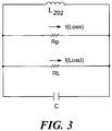
- a tank circuit can be modeled as a primary winding inductance L 202 in parallel with the a capacitance C across the primary winding and further in parallel with an actual load resistance RL and a resistance Rp, which represents the tank dissipation and is given by the formula Rs(Q 2 +1), where R s is the series resistance of the primary winding.
- Rp represents the tank dissipation and is given by the formula Rs(Q 2 +1), where R s is the series resistance of the primary winding.
- the relationship between Rp and RL determines the efficiency of the tank circuit. If Rp is infinitely large, all of the energy gets transferred to load resistance RL. The smaller the value of Rp, the greater the percentage of the energy of the tank that is lost in Rp and is unavailable for transfer to the load.
- Some power savings can be achieved by not energizing the tank circuit all of the time. For a certain percentage of the time, it can be de-energized and a sufficient amount of power will still be transferred into the load. This ability depends on load power requirements.
- the state of switch 212 is controlled by a pulse-width modulator (PWM) signal supplied on line 214.
- PWM pulse-width modulator
- Transformer TR2 is thus driven by a modulated signal such that power is transferred at greater efficiency, with the average power being controlled through the average "on" time of the LC tank circuit.
- This control eliminates the need to control the duty cycle of the high frequency signal going into the primary coil, as in a typical full-bridge converter such as that shown in FIG. 1 .
- the signal on secondary winding 204 is provided through a rectifier 216 to a capacitive filter 218 with capacitor C2 can be employed.
- the capacitor may be external to the chip, but some on-chip capacitance also is desirable because external by-pass capacitors also have high equivalent series inductance (ESL).
- ESL equivalent series inductance
- a dynamic switching controller circuit can be implemented as shown in FIG. 2A .
- This controller monitors the output voltage and compares it with a reference voltage from a reference source 226 in a comparator 224.
- the voltage that is compared can be scaled down from the output voltage at node 222 by using a resistive voltage divider with resistors R1 and R2 connected at node 228, and thus the voltage at node 228 is actually compared with the reference voltage from reference source 226. If the voltage on node 228 is higher than the reference voltage (i.e., higher than required), the output of comparator 224 is driven to a low value, which is supplied to an encoder 232 via a line 234.
- Encoder 232 drives a primary winding 242 of a transformer TR3 with a signal, and a secondary winding 244 of transformer TR3 couples a corresponding signal to an input of a decoder 246.
- decoder 246 emits a control signal on line 214 to control the LC tank network. If the scaled output voltage on node 228 falls below the threshold established by reference source 226, the output of comparator 224 becomes high, and the encoder 232 transmits a corresponding signal through transformer TR3 to decoder 246. Decoder 246 then transmits a control signal on line 214 to close switch 212 to allow the LC tank to oscillate.
- the actual output voltage at node 222 depends on the output current, due to the series resistance of the secondary coil 204 of the power transformer TR2, thereby making regulation possible.
- Transformers TR2 and TR3 are preferably micro-transformers. The same process can be used to manufacture power transformer TR2 and control signal transformer TR3, or they could be made separately in different ways.
- the circuitry on the "left" side of the two transformers is referenced to a first ground, GNDA (indicated by a black-filled downwardly-pointing triangle), whereas the circuitry to the "right” side of the two transformers is referenced to a different ground, GNDB, electrically isolated from the first ground (indicated by an open downwardly-pointing triangle).
- FIG. 2B shows an exemplary set of waveforms for the circuit of FIG. 2A .
- the output voltage at node 222 is shown as a DC signal of about 5 volts with a ripple that may be, e.g., about +/- 50 mV.
- comparator 224 When the signal on node 222 falls below a threshold, comparator 224 outputs a high signal on line 234.
- This signal is provided to an encoder 232 that provides an encoded signal.
- One example of such an encoded signal as shown in FIG. 2B is to use a dual pulse for a rising edge and a single pulse for a falling edge.
- Decoder 246 detects the encoded signal and generates a delayed and inverted version of the signal on line 234 to open and close switch 212.
- switch 212 closes to allow the tank circuit to provide an oscillating signal, at a frequency determined by the components of the tank circuit, e.g., at about 100 MHz.
- This signal is then provided by secondary winding 204 to rectifier 216.
- the rectified signal is filtered by capacitive filter 218 to produce a signal similar to that shown in FIG. 2B for node 222.
- the coil driver, rectifier, and capacitive filter are similar to those in FIG. 2A , but the controller circuitry is implemented in a different configurations.
- the scaled down output voltage is provided to an amplifier 402 (replacing comparator 224 of FIG. 2A ) to produce an error voltage.
- the error voltage is compared in comparator 406 with a (fixed-frequency) saw-tooth wave signal from a saw-tooth wave generator 404.
- a fixed-frequency PWM control signal is generated on line 408 and provided to encoder 232 to control a switch in a manner similar to that shown in FIG. 2A .
- a rectifier 410 in FIG. 4 can be a simple bridge circuit (comprising diodes D1-D4) with capacitor C2 serving as a capacitive filter and with no series filter inductor at the output of the rectifier.
- Other rectification configurations may be employed.
- a rectifier has only two diodes, D1 and D3, with a center-tapped secondary transformer winding 204' as part of transformer TR2.
- a power converter can be implemented with the control signal for the PWM tank switch being set to a certain duty cycle that is fixed or programmed by some other means.
- These arrangements can be configured by selecting the turns ratio of the windings of transformer TR2 to provide either a step up or a step down voltage transfer, depending on the particular desired output voltage to input voltage relationship.
- the secondary winding has two times the number of windings in the primary winding, and thus has four times the inductance of the primary winding.
- the power that is transferred across transformer TR2 would typically be greater than 100 mW and could be more than 500 mW, and could be up to 1 W (or possibly greater).
- micro-transformers for logical data transfer and power transfer, and also as needed for other control signals in the feedback path, can make it easier to integrate all of the isolation functions.
- the same manufacturing processes can be used to make all the transformers, although different processes could be used.
- any number of data channels, unidirectional or bidirectional, can be added, to provide an arbitrary number of self-powered isolators.
- a single transformer can be used for both power and data transfer. For example, an input digital signal or a signal derived therefrom can be used to control tank switch 212; and a receiver can be added to decode the input digital signal from the modulated signal in the power converter.
- any suitable micro-transformer design can be used, but in these embodiments the micro-transformers discussed herein are preferably core-less transformers, sometimes referred to as "air core” transformers, and preferably on-chip; however, the circuits described here could be used with transformers with ferrous cores, micro-transformers formed on opposite sides of a PCB, or with transformers formed with known discrete wire windings.
- core-less transformers efficiency can be obtained by (a) manufacturing the transformer windings very close together, and (b) operating the transformers at high frequencies.
- cores can add thickness, weight, and cost, and can also require the use of lower frequencies.
- One material that is often used to fabricate metal layers in integrated circuits is aluminum. When the metal layer is to be used for a coil winding for a transformer, it can be helpful to increase the thickness of the bottom coil in order to lower its resistance and increase its L/R ratio.
- One or both coil windings may be formed of a non-process metal, i.e., a metal different from that used in the processing that forms the semiconductor devices and circuitry.
- the transformers may be fabricated of gold or another metal that is deposited over a substrate that already contains circuit elements. This approach allows the coil windings to be made thicker than typical metal layers in, for example, a CMOS process used to form the switching transistors and other components.
- an on-chip micro-transformer has three layers of metal, such that the layers from substrate outwardly are substrate, wafer passivation layer, a first metal layer is over the wafer passivation layer for connection from a bond pad to a center of a spiral, a first insulating layer, a first bottom winding connected to the first metal layer through a via, a second insulating layer, and a second top winding.
- a dielectric such as an oxide or polyimide layer, as thick as desired, may be formed over the substrate and the coil windings can then be formed on top of this layer.
- Polyimide is an example of a dielectric that can be used for such a structure, and for use in separating the windings, as it tends to have better electrostatic discharge properties and resist punch through better than many oxides, although oxides could be used.
- the two transformers TR2 and TR3 can, but need not, have identical construction.
- coil 244 in transformer TR3 does not need to have a low resistance and therefore can be made differently from other coils.
- FIGS. 2A , 4 , and 5 The power transfer (DC-DC converter) arrangements illustrated in FIGS. 2A , 4 , and 5 can be combined with isolators such as those disclosed in the incorporated patents and applications to provide low-cost signal and power transfer and isolation in an integrated circuit package, manufactured using integrated circuit fabrication techniques.
- this diagrammatic illustration shows how a power converter can be formed on two substrates 602 and 604.
- a logical signal input supplied at node 606, the circuitry on substrate 602, and one coil of each of transformers TR5, TR6, and TR7 are referenced to a first ground, GNDA.
- These transformers can be micro-transformers, and can be core-less on-chip transformers.
- a signal output supplied at node 608, the circuitry on substrate 604, and another coil of each of the transformers are referenced to a second ground, GNDB.
- a transmitter circuit 610 receives an input information (e.g., logic) signal applied to node 606 and drives a primary winding 612 of a transformer TR7.
- a secondary winding 614 of transformer TR7 provides a corresponding waveform to a receiver circuit 616.
- the receiver circuit decodes the received waveform and constructs an output signal 608 that reproduces input signal 606.
- the operation and construction of the transmitter and receiver circuits may, for example, be as discussed in the incorporated documents.
- a coil driver 620 receives an input from Vdd and drives a primary winding of transformer TR6.
- the secondary winding of transformer TR6 is provided to a rectifier 622 with filtering (not shown) to provide a regulated power converter output at node 630.
- the power converter output is also fed back to a feedback controller, represented by comparator 624 (which includes both the sensing and comparison circuits of FIGS. 2 , 4 , and 5 , and the encoder 232), which provides the signal to a primary winding of transformer TR5.
- the secondary winding of TR5 provides a signal to a decoder 246, which provides a control signal to control the connection between the supply voltage and the coil driver 620, such as by controlling a switch as shown in FIG. 2A .
- the isolator circuitry and power converter circuitry can be packaged in any suitable manner. For example, there could be multiple isolators powered by a single power converter, or there might be provided bi-directional isolators.
- the power converter can supply isolated power for a receiving circuit of one or more isolators and for the transmitter circuit of one or more other isolators (or channels).
- the transformers are shown as being fabricated on substrate 604, but could be fabricated on substrate 602. While FIG. 6 shows an implementation with two substrates, more substrates could be used, e.g., with one or more of the transformers together on one or more separate substrates that do not have transmitter, receiver, driver, encoding, or decoding circuitry.
- a micro-transformer-based power converter can be used to drive an output circuit, such as an output with isolated-gate field effect transistors (IGFETs), in a way that provides power and logic information.
- IGFETs isolated-gate field effect transistors
- FIGS. 7A and 8A depict two examples of IGFET drivers, with FIG. 7A having two transformers for separately providing logic and power, and FIG. 8A modulating the power converter to provide power and logic.
- a voltage supply is coupled through a switch 212 to a coil driver that drives a transformer in a manner similar to that in the circuitry in FIG. 2A .
- a FET IN logic signal shown in FIG. 7B
- a driver 726 that uses the input frequency and the output capacitance of the system as factors to provide a control signal 722 with a frequency of about 1 MHz to control switch 212.
- the signal has half the period and is inverted and delayed compared to FET IN.
- the switch When signal 722 is low, the switch is closed and the signal across coil 202 (and hence coil 204) oscillates between +5 volts and -5 volts at a high frequency, such as a frequency over 10 MHz, and preferably at about 100 MHz.
- Coil 204 is tapped to provide three signals, each of which is provided to a separate forward biased diode in parallel with a capacitor to provide regulated voltages at +15, +10, and +5 volts, and with a ground isolated from the input side of the transformer.
- the FET IN signal is also provided through an encoder 724, transformer 720, and decoder 710 in a manner similar to that in FIG. 2A , as shown by the signal in FIG. 7B across transformer 720.
- the voltage inputs to encoder 710 are 5 volts and 0 volts, so the output of decoder 710 is an isolated logic signal that mimics FET IN.
- the output of decoder 710 is provided to a low side FET driver 708 and also to a level shifter 712 and then to high side FET driver 706.
- the level shifter shifts the signal from decoder 710 from a range of 0-5 volts, to a range of 10-15 volts.
- Amplifiers 706 and 708 are each coupled to the gates of IGFETs 702 and 704, respectively.
- the resulting FET OUT signal is a delayed version of FET IN, and is provided at 15 volts.
- FIG. 8A is another embodiment that utilizes a similar principle to FIG. 7A , but uses one transformer for power and information transfer across an isolation barrier.
- a FET IN signal controls a switch between a voltage supply and a coil driver that drives a tank circuit, and thereby modulates the power output.
- the FET IN signal controls the switch and the tank circuit provides a high frequency oscillating signal when the switch is closed, e.g., at greater than 10 MHz and preferably greater than 100 MHz.
- the secondary winding is tapped, and each of the lines from the transformer is provided to a separate diode in parallel with a capacitor to produce regulated outputs at +15, +10, and +5 volts.
- the +5 volt output at node 810 drives a resistive load 808 and is also provided to a level shifter 816 and then to a first driver 814 powered between 15 volt and 10 volt supplies, and also to a second driver 812 powered between a 5 volt supply and ground.
- Level shifter 816 translates the signal into the second driver 812 into a correct voltage range to drive the first driver 814. As shown in FIG.
- the signal at node 810 is inverted from FET IN and, when high, has a small ripple.
- the output from level shifter 816 is similar, but is between +15 and +10 volts.
- the resulting FET OUT signal is between 15 and 0 volts and follows the FET IN logic signal.
- FIG. 9 is an example of a non-isolated power converter 900 that uses some similar principles to the circuits described above, including an aspect of the coil driver in FIG. 2A .
- a voltage input VIN is coupled to a switch 902 controlled by a relatively low frequency signal, Vcontrol, and a coil driver 904 formed as a cross-coupled PMOS transistors with the source of each transistor coupled to the gate of the other transistor to provide a positive feedback.
- Coil driver 904 is coupled to a tank circuit 906 with a first inductor L1 in parallel with a capacitor C3 and a second inductor L2.
- Tank circuit 906 produces a high frequency oscillation that is provided to a rectifier 908 and then a filtering capacitor C4 to provide an output VOUT.
- the control signal to switch 902 can have a frequency of about 1 MHz, while the tank circuit has a much higher frequency, e.g., 100 MHz. This circuit preferably does not have an inductor in series with then output from the rectifier.
Landscapes
- Engineering & Computer Science (AREA)
- Power Engineering (AREA)
- Dc-Dc Converters (AREA)
- Logic Circuits (AREA)
- Power Conversion In General (AREA)
Applications Claiming Priority (3)
| Application Number | Priority Date | Filing Date | Title |
|---|---|---|---|
| US10/922,504 US7489526B2 (en) | 2004-08-20 | 2004-08-20 | Power and information signal transfer using micro-transformers |
| PCT/US2005/029617 WO2006023767A2 (fr) | 2004-08-20 | 2005-08-19 | Transfert d'energie et de signaux d'information au moyen de micro-transformateurs |
| EP05789057.6A EP1787382B1 (fr) | 2004-08-20 | 2005-08-19 | Transfert d'énergie et de signaux d'information au moyen de micro-transformateurs |
Related Parent Applications (2)
| Application Number | Title | Priority Date | Filing Date |
|---|---|---|---|
| EP05789057.6A Division-Into EP1787382B1 (fr) | 2004-08-20 | 2005-08-19 | Transfert d'énergie et de signaux d'information au moyen de micro-transformateurs |
| EP05789057.6A Division EP1787382B1 (fr) | 2004-08-20 | 2005-08-19 | Transfert d'énergie et de signaux d'information au moyen de micro-transformateurs |
Publications (3)
| Publication Number | Publication Date |
|---|---|
| EP3157152A2 true EP3157152A2 (fr) | 2017-04-19 |
| EP3157152A3 EP3157152A3 (fr) | 2017-05-10 |
| EP3157152B1 EP3157152B1 (fr) | 2019-10-23 |
Family
ID=35909417
Family Applications (2)
| Application Number | Title | Priority Date | Filing Date |
|---|---|---|---|
| EP05789057.6A Expired - Lifetime EP1787382B1 (fr) | 2004-08-20 | 2005-08-19 | Transfert d'énergie et de signaux d'information au moyen de micro-transformateurs |
| EP16200733.0A Expired - Lifetime EP3157152B1 (fr) | 2004-08-20 | 2005-08-19 | Transfert d'énergie et de signaux d'information à l'aide de micro-transformateurs |
Family Applications Before (1)
| Application Number | Title | Priority Date | Filing Date |
|---|---|---|---|
| EP05789057.6A Expired - Lifetime EP1787382B1 (fr) | 2004-08-20 | 2005-08-19 | Transfert d'énergie et de signaux d'information au moyen de micro-transformateurs |
Country Status (6)
| Country | Link |
|---|---|
| US (4) | US7489526B2 (fr) |
| EP (2) | EP1787382B1 (fr) |
| JP (1) | JP4659037B2 (fr) |
| KR (2) | KR100961293B1 (fr) |
| CN (3) | CN101189786B (fr) |
| WO (1) | WO2006023767A2 (fr) |
Cited By (1)
| Publication number | Priority date | Publication date | Assignee | Title |
|---|---|---|---|---|
| WO2020263886A1 (fr) * | 2019-06-24 | 2020-12-30 | Texas Instruments Incorporated | Barrière d'isolation de données et de puissance |
Families Citing this family (69)
| Publication number | Priority date | Publication date | Assignee | Title |
|---|---|---|---|---|
| DE10243197B4 (de) * | 2002-09-18 | 2011-05-05 | Infineon Technologies Ag | Digitales Signalübertragungsverfahren |
| WO2004100473A2 (fr) * | 2003-04-30 | 2004-11-18 | Analog Devices, Inc. | Isolateurs de signal utilisant des micro-transformateurs |
| US7256920B2 (en) * | 2004-10-30 | 2007-08-14 | Bookham Technology Plc | Electro-optic modulator |
| US7463397B2 (en) * | 2005-12-20 | 2008-12-09 | Bookham Technology Plc | Electro-optic modulator |
| US7719305B2 (en) * | 2006-07-06 | 2010-05-18 | Analog Devices, Inc. | Signal isolator using micro-transformers |
| EP1901428A1 (fr) * | 2006-09-14 | 2008-03-19 | St Microelectronics S.A. | Transfert de données numériques à travers un transformateur |
| JP2008218120A (ja) * | 2007-03-02 | 2008-09-18 | Fuji Electric Device Technology Co Ltd | 信号伝送装置 |
| US7921308B2 (en) * | 2007-05-24 | 2011-04-05 | Akros Silicon, Inc. | Power signal merging for network interface devices |
| FR2918817A1 (fr) | 2007-07-12 | 2009-01-16 | St Microelectronics Sa | Circuit de commande d'un commutateur alternatif. |
| EP2045791B1 (fr) * | 2007-10-01 | 2014-01-15 | Siemens Aktiengesellschaft | Dispositif électronique |
| US8084894B2 (en) * | 2008-02-04 | 2011-12-27 | Analog Devices, Inc. | Solid state relay |
| JP2009232052A (ja) * | 2008-03-21 | 2009-10-08 | Fuji Electric Device Technology Co Ltd | データ伝送装置 |
| US7983059B2 (en) * | 2008-09-02 | 2011-07-19 | Analog Devices, Inc. | High frequency power converter based on transformers |
| US20100073980A1 (en) * | 2008-09-23 | 2010-03-25 | Gm Global Technology Operations, Inc. | Power converter assembly with isolated gate drive circuit |
| US8319573B2 (en) * | 2009-12-23 | 2012-11-27 | Infineon Technologies Austria Ag | Signal transmission arrangement |
| FR2955422B1 (fr) | 2010-01-21 | 2017-03-17 | Rwaytech | Transformateur sans noyau a haute isolation galvanique |
| TWI398081B (zh) * | 2010-03-12 | 2013-06-01 | Richtek Technology Corp | 降低功率耗損的電源供應器 |
| US9716440B2 (en) | 2011-05-18 | 2017-07-25 | Renasas Electronics Corporation | Receiving circuit and signal receiving method |
| US8890368B2 (en) | 2011-06-27 | 2014-11-18 | Maxim Integrated Products, Inc. | Systems and methods for power transfer based on resonance coupling of inductors |
| DE102011080270A1 (de) * | 2011-08-02 | 2013-02-07 | Siemens Ag Österreich | Rekonfigurierbare Leistungsschalteranordnung |
| US8625242B2 (en) | 2011-08-03 | 2014-01-07 | Maxim Integrated Products, Inc. | Failsafe galvanic isolation barrier |
| US8558344B2 (en) | 2011-09-06 | 2013-10-15 | Analog Devices, Inc. | Small size and fully integrated power converter with magnetics on chip |
| JP5644810B2 (ja) | 2011-09-26 | 2014-12-24 | 株式会社デンソー | 信号および電力の伝送装置 |
| US8837170B2 (en) * | 2011-12-13 | 2014-09-16 | Busek Company | Passive resonant bidirectional converter with galvanic barrier |
| US9231463B2 (en) * | 2012-08-06 | 2016-01-05 | Peter Oaklander | Noise resistant regulator including an encoded control signal |
| US8786393B1 (en) | 2013-02-05 | 2014-07-22 | Analog Devices, Inc. | Step up or step down micro-transformer with tight magnetic coupling |
| US9929038B2 (en) | 2013-03-07 | 2018-03-27 | Analog Devices Global | Insulating structure, a method of forming an insulating structure, and a chip scale isolator including such an insulating structure |
| US9293997B2 (en) | 2013-03-14 | 2016-03-22 | Analog Devices Global | Isolated error amplifier for isolated power supplies |
| KR102087283B1 (ko) * | 2013-09-10 | 2020-03-11 | 이피션트 파워 컨버젼 코퍼레이션 | 고효율 전압 모드 클래스 d 토폴로지 |
| JP6217685B2 (ja) * | 2014-05-09 | 2017-10-25 | 株式会社豊田自動織機 | 電源装置 |
| US10270630B2 (en) | 2014-09-15 | 2019-04-23 | Analog Devices, Inc. | Demodulation of on-off-key modulated signals in signal isolator systems |
| US9660848B2 (en) | 2014-09-15 | 2017-05-23 | Analog Devices Global | Methods and structures to generate on/off keyed carrier signals for signal isolators |
| US10536309B2 (en) | 2014-09-15 | 2020-01-14 | Analog Devices, Inc. | Demodulation of on-off-key modulated signals in signal isolator systems |
| US9998301B2 (en) | 2014-11-03 | 2018-06-12 | Analog Devices, Inc. | Signal isolator system with protection for common mode transients |
| US9525411B2 (en) | 2014-11-13 | 2016-12-20 | Analog Devices, Inc. | Power supply circuits for gate drivers |
| ITUB20153500A1 (it) * | 2015-09-09 | 2017-03-09 | St Microelectronics Srl | Procedimento per trasmettere potenza e dati attraverso una barriera di isolamento galvanico, sistema ed apparecchiatura corrispondenti |
| US9941565B2 (en) | 2015-10-23 | 2018-04-10 | Analog Devices Global | Isolator and method of forming an isolator |
| US10204732B2 (en) | 2015-10-23 | 2019-02-12 | Analog Devices Global | Dielectric stack, an isolator device and method of forming an isolator device |
| ITUB20156047A1 (it) | 2015-12-01 | 2017-06-01 | St Microelectronics Srl | Sistema di isolamento galvanico, apparecchiatura e procedimento |
| US10097096B2 (en) | 2016-05-04 | 2018-10-09 | Toyota Motor Engineering & Manufacturing North America, Inc. | Packaging of a power conversion circuit |
| US9948193B2 (en) * | 2016-06-10 | 2018-04-17 | Stmicroelectronics S.R.L. | Galvanically isolated DC-DC converter with bidirectional data transmission |
| IT201600088207A1 (it) | 2016-08-30 | 2018-03-02 | St Microelectronics Srl | Circuito di isolamento galvanico, sistema e procedimento corrispondenti |
| US9978696B2 (en) | 2016-09-14 | 2018-05-22 | Analog Devices, Inc. | Single lead-frame stacked die galvanic isolator |
| US9812989B1 (en) * | 2016-09-20 | 2017-11-07 | Silicon Laboratories Inc. | Isolated power transfer device |
| DE102016222408A1 (de) * | 2016-11-15 | 2018-05-17 | Fraunhofer-Gesellschaft zur Förderung der angewandten Forschung e.V. | Energieversorgungsvorrichtung und Verfahren zum Bereitstellen einer Ausgangsspannung |
| US10680526B2 (en) * | 2017-01-13 | 2020-06-09 | Analog Devices Global | Power transfer and feedback across a common isolator |
| FR3072520B1 (fr) | 2017-10-16 | 2020-09-04 | St Microelectronics Tours Sas | Circuit de commande d'un thyristor ou triac |
| US10511273B2 (en) | 2017-12-07 | 2019-12-17 | Silicon Laboratories Inc. | Power transfer device using an oscillator |
| US10326375B1 (en) | 2017-12-07 | 2019-06-18 | Silicon Laboratories Inc. | Isolated power transfer with integrated transformer and voltage control |
| EP3512087B1 (fr) | 2018-01-12 | 2023-01-25 | STMicroelectronics S.r.l. | Circuit de convertisseur cc-cc galvaniquement isolé à communication de données, système correspondant et procédé correspondant |
| US10826334B2 (en) | 2018-03-29 | 2020-11-03 | Silicon Laboratories Inc. | Electromagnetic radiation control for isolated power transfer product |
| US11482924B2 (en) * | 2018-07-26 | 2022-10-25 | Analog Devices International Unlimited Company | Power isolator exhibiting low electromagnetic interference |
| US11044022B2 (en) | 2018-08-29 | 2021-06-22 | Analog Devices Global Unlimited Company | Back-to-back isolation circuit |
| US10833535B2 (en) | 2018-09-25 | 2020-11-10 | Silicon Laboratories Inc. | Power resonator with wide input voltage range for isolated power transfer |
| US10797609B2 (en) | 2019-02-26 | 2020-10-06 | Analog Devices International Unlimited Company | Systems and methods for transferring power across an isolation barrier using an active self synchronized rectifier |
| US10790754B2 (en) | 2019-02-26 | 2020-09-29 | Analog Devices International Unlimited Company | Systems and methods for transferring power across an isolation barrier using an active resonator |
| CN109831202A (zh) * | 2019-03-07 | 2019-05-31 | 北京中科格励微科技有限公司 | 线性隔离器 |
| CN109741921B (zh) * | 2019-03-21 | 2024-07-26 | 东莞市德奥智能电子有限公司 | 一种抑制电磁干扰高频变压器的绕制结构 |
| CN109995357A (zh) * | 2019-04-23 | 2019-07-09 | 北京中科格励微科技有限公司 | 线性隔离器 |
| US11450469B2 (en) | 2019-08-28 | 2022-09-20 | Analog Devices Global Unlimited Company | Insulation jacket for top coil of an isolated transformer |
| US11533027B2 (en) | 2019-10-18 | 2022-12-20 | Analog Devices, Inc. | Low power receiver circuit for isolated data communications |
| US11387316B2 (en) | 2019-12-02 | 2022-07-12 | Analog Devices International Unlimited Company | Monolithic back-to-back isolation elements with floating top plate |
| JP2022125703A (ja) * | 2021-02-17 | 2022-08-29 | キヤノン株式会社 | 振動型駆動装置 |
| US11689174B2 (en) | 2021-06-01 | 2023-06-27 | Skyworks Solutions, Inc. | Isolation communications channel using direct demodulation and data-edge encoding |
| US12607117B2 (en) * | 2021-09-29 | 2026-04-21 | Halliburton Energy Services, Inc. | Solid state tuning with coupled inductors for downhole systems |
| US20250125770A1 (en) * | 2022-02-16 | 2025-04-17 | University Of Science And Technology Of China | Isolated power supply chip based on symmetrical class-d oscillator with dead zone control |
| JP7815887B2 (ja) * | 2022-03-14 | 2026-02-18 | サンケン電気株式会社 | 半導体回路 |
| CN219697495U (zh) * | 2023-04-28 | 2023-09-15 | 上海晶丰明源半导体股份有限公司 | 开关模式功率转换器 |
| WO2025043224A2 (fr) * | 2023-08-23 | 2025-02-27 | Mixed-Signal Devices Inc. | Circuits redresseurs pleine onde à grande vitesse utilisant un mosfet |
Citations (2)
| Publication number | Priority date | Publication date | Assignee | Title |
|---|---|---|---|---|
| US6291907B1 (en) | 1997-10-23 | 2001-09-18 | Analog Devices, Inc. | Magnetically coupled signal isolator using a faraday shielded MR or GMR receiving element |
| US20030042571A1 (en) | 1997-10-23 | 2003-03-06 | Baoxing Chen | Chip-scale coils and isolators based thereon |
Family Cites Families (60)
| Publication number | Priority date | Publication date | Assignee | Title |
|---|---|---|---|---|
| JPS5649075B2 (fr) * | 1974-01-23 | 1981-11-19 | ||
| US4065713A (en) * | 1974-09-13 | 1977-12-27 | Nixdorf Computer Ag | Voltage stabilizer |
| US4035710A (en) * | 1975-10-20 | 1977-07-12 | International Business Machines Corporation | Pulse width modulated voltage regulator-converter/power converter having means for improving the static stability characteristics thereof |
| US4024452A (en) * | 1976-03-10 | 1977-05-17 | Bell Telephone Laboratories, Incorporated | Integrated solid state isolator circuit |
| US4443839A (en) | 1980-12-23 | 1984-04-17 | Tokyo Shibaura Denki Kabushiki Kaisha | Single ended, separately driven, resonant DC-DC converter |
| US4318170A (en) | 1981-01-12 | 1982-03-02 | Cabalfin Rolando V | Power inverter oscillator circuit |
| US4475149A (en) | 1982-09-13 | 1984-10-02 | Venus Scientific Inc. | Resonant current-driven power source |
| US4785345A (en) | 1986-05-08 | 1988-11-15 | American Telephone And Telegraph Co., At&T Bell Labs. | Integrated transformer structure with primary winding in substrate |
| US4720667A (en) * | 1986-06-20 | 1988-01-19 | Lee Fred C | Zero-current switching quasi-resonant converters operating in a full-wave mode |
| DE3731644A1 (de) | 1987-09-19 | 1989-03-30 | Thomson Brandt Gmbh | Schaltungsanordnung fuer ein geregeltes schaltnetzteil |
| US5327030A (en) | 1987-11-13 | 1994-07-05 | Analog Devices, Inc. | Decoder and monolithic integrated circuit incorporating same |
| JPH0648904B2 (ja) * | 1988-09-05 | 1994-06-22 | オリジン電気株式会社 | 並列形共振コンバータ |
| US4882666A (en) * | 1989-03-23 | 1989-11-21 | North American Philips Corporation | High frequency high voltage power supply with controlled output power |
| US4920474A (en) | 1989-03-23 | 1990-04-24 | North American Philips Corporation | High frequency high voltage power supply with controlled output power |
| DE69121043D1 (de) | 1990-10-18 | 1996-08-29 | Valor Electronics Inc | Nicht-gekoppelte integrierte magnetische Struktur |
| US5450305A (en) * | 1991-08-12 | 1995-09-12 | Auckland Uniservices Limited | Resonant power supplies |
| JP3132093B2 (ja) * | 1991-09-25 | 2001-02-05 | ヤマハ株式会社 | 電源回路 |
| US5430641A (en) * | 1992-04-27 | 1995-07-04 | Dell Usa, L.P. | Synchronously switching inverter and regulator |
| JP2803943B2 (ja) * | 1992-10-21 | 1998-09-24 | アルプス電気株式会社 | 非接触電力供給装置 |
| US5329225A (en) | 1992-11-02 | 1994-07-12 | General Electric Co. | Thin film superconductor inductor with shield for high frequency resonant circuit |
| US5339061A (en) | 1993-06-01 | 1994-08-16 | Michael Ebert | Iron-free transformer |
| CN1050242C (zh) | 1993-06-14 | 2000-03-08 | Vlt公司 | 电源变换装置、电源变换器控制装置及其制造电源变换器的方法 |
| JPH07115768A (ja) * | 1993-10-14 | 1995-05-02 | Japan Storage Battery Co Ltd | 共振形コンバータ |
| US5636110A (en) | 1994-04-26 | 1997-06-03 | Comarco Wireless Technologies, Inc. | Small form factor power supply |
| GB9421402D0 (en) | 1994-10-21 | 1994-12-07 | Plessey Semiconductors Ltd | Power switch driver |
| US5774350A (en) | 1995-04-07 | 1998-06-30 | Sgs-Thomson Microelectronics S.A. | Integrated low dissipation power controller |
| JPH0937558A (ja) * | 1995-07-14 | 1997-02-07 | Yokogawa Electric Corp | インバータ装置 |
| JPH10191654A (ja) * | 1996-12-24 | 1998-07-21 | Harumi Suzuki | インバータ回路およびその回路を用いた照明装置 |
| WO1998050993A1 (fr) * | 1997-05-06 | 1998-11-12 | Auckland Uniservices Limited | Transfert d'energie inductif a travers un espace etendu |
| SE520906C2 (sv) | 1997-10-28 | 2003-09-09 | Ericsson Telefon Ab L M | Spänningsregulator med ett mycket lågt 'drop-out voltage' |
| JP3247328B2 (ja) | 1997-12-09 | 2002-01-15 | 浩 坂本 | 非接触電力伝達装置 |
| US6025705A (en) | 1997-12-24 | 2000-02-15 | Intel Corporation | DC-to-DC converter |
| US6215374B1 (en) | 1998-03-16 | 2001-04-10 | Broadband Innovations, Inc. | Magnetically coupled resonators for achieving low cost narrow band pass filters having high selectivity, low insertion loss and improved out-of-band rejection |
| JP3705966B2 (ja) | 1999-09-07 | 2005-10-12 | 東光株式会社 | スイッチング電源回路 |
| KR20010093794A (ko) * | 1999-09-29 | 2001-10-29 | 추후기재 | 높은 선택도, 낮은 삽입 손실 및 확장된 주파수 범위에대해 개량된 대역외 저지를 갖는 협대역 통과 동조 공진기필터 토폴로지 |
| US6738240B1 (en) * | 1999-12-10 | 2004-05-18 | Micron Technology, Inc. | Microtransformer for system-on-chip power supply |
| EP1469584B1 (fr) | 2000-02-24 | 2009-08-05 | Panasonic Electric Works Co., Ltd. | Système de transmission de puissance avec fonction de maintenir constante la tension de charge |
| FI20002493A7 (fi) * | 2000-11-14 | 2002-05-15 | Salcomp Oy | Teholähdejärjestely ja induktiivisesti kytketty akkulaturi, jossa on langattomasti kytketty ohjaus, ja menetelmä teholähdejärjestelyn ja induktiivisesti kytketyn akkulaturin ohjaamiseksi langattomasti |
| US6341073B1 (en) * | 2000-11-16 | 2002-01-22 | Philips Electronics North America Corporation | Multiple valley controller for switching circuit |
| US6542385B1 (en) | 2000-11-22 | 2003-04-01 | Teradyne, Inc. | DUT power supply having improved switching DC-DC converter |
| SE0004794L (sv) | 2000-12-22 | 2002-06-23 | Ericsson Telefon Ab L M | En flerskikts-symmetreringstransformatorstruktur |
| US6344979B1 (en) | 2001-02-09 | 2002-02-05 | Delta Electronics, Inc. | LLC series resonant DC-to-DC converter |
| JP4074064B2 (ja) * | 2001-02-28 | 2008-04-09 | 株式会社東芝 | 半導体装置 |
| US7285919B2 (en) | 2001-06-22 | 2007-10-23 | Lutron Electronics Co., Inc. | Electronic ballast having improved power factor and total harmonic distortion |
| US6993087B2 (en) | 2001-06-29 | 2006-01-31 | Nokia Mobile Phones Ltd. | Switching mode power amplifier using PWM and PPM for bandpass signals |
| JP2003203800A (ja) * | 2001-09-14 | 2003-07-18 | Sekisui Chem Co Ltd | 常圧プラズマ処理方法および装置 |
| US6765809B2 (en) | 2001-10-09 | 2004-07-20 | Samsung Electronics Co., Ltd. | Power source circuit having regulated primary current |
| US6606260B2 (en) | 2001-10-29 | 2003-08-12 | The Chamberlain Group, Inc. | Switch mode power supply for a telephone entry system or the like |
| AU2002365723A1 (en) * | 2001-12-05 | 2003-06-17 | Koninklijke Philips Electronics N.V. | Voltage converter for a power supply |
| US6807070B2 (en) | 2001-12-12 | 2004-10-19 | International Rectifier Corporation | Resonant converter with phase delay control |
| US6801114B2 (en) | 2002-01-23 | 2004-10-05 | Broadcom Corp. | Integrated radio having on-chip transformer balun |
| US6975098B2 (en) | 2002-01-31 | 2005-12-13 | Vlt, Inc. | Factorized power architecture with point of load sine amplitude converters |
| TWI222266B (en) | 2002-02-14 | 2004-10-11 | Kazuo Kohno | Self oscillation circuits |
| US6621365B1 (en) * | 2002-04-03 | 2003-09-16 | Nokia Corporation | Method and apparatus providing a dual mode VCO for an adaptive receiver |
| MXPA04009647A (es) | 2002-04-04 | 2005-01-11 | Thomson Licensing Sa | Regulador de conmutacion de frecuencia de linea. |
| DE10232642B4 (de) | 2002-07-18 | 2006-11-23 | Infineon Technologies Ag | Integrierte Transformatoranordnung |
| KR100892584B1 (ko) * | 2002-08-26 | 2009-04-08 | 삼성전자주식회사 | 전원공급장치와 이를 갖는 백라이트 어셈블리 및 액정표시 장치 |
| WO2004100473A2 (fr) | 2003-04-30 | 2004-11-18 | Analog Devices, Inc. | Isolateurs de signal utilisant des micro-transformateurs |
| US7098766B2 (en) | 2004-01-21 | 2006-08-29 | Intel Corporation | Magnetic material for transformers and/or inductors |
| US7116183B2 (en) * | 2004-02-05 | 2006-10-03 | Qualcomm Incorporated | Temperature compensated voltage controlled oscillator |
-
2004
- 2004-08-20 US US10/922,504 patent/US7489526B2/en not_active Expired - Lifetime
-
2005
- 2005-08-19 EP EP05789057.6A patent/EP1787382B1/fr not_active Expired - Lifetime
- 2005-08-19 CN CN2005800329554A patent/CN101189786B/zh not_active Expired - Lifetime
- 2005-08-19 EP EP16200733.0A patent/EP3157152B1/fr not_active Expired - Lifetime
- 2005-08-19 US US11/594,328 patent/US7548440B2/en not_active Expired - Lifetime
- 2005-08-19 CN CN201510046516.4A patent/CN104734515B/zh not_active Expired - Fee Related
- 2005-08-19 KR KR1020097023827A patent/KR100961293B1/ko not_active Expired - Fee Related
- 2005-08-19 JP JP2007528054A patent/JP4659037B2/ja not_active Expired - Lifetime
- 2005-08-19 WO PCT/US2005/029617 patent/WO2006023767A2/fr not_active Ceased
- 2005-08-19 KR KR1020077006363A patent/KR100975484B1/ko not_active Expired - Lifetime
- 2005-08-19 CN CN201110235730.6A patent/CN102324851B/zh not_active Expired - Lifetime
-
2006
- 2006-11-06 US US11/593,385 patent/US7706154B2/en not_active Expired - Lifetime
- 2006-11-06 US US11/593,360 patent/US7613016B2/en not_active Expired - Lifetime
Patent Citations (2)
| Publication number | Priority date | Publication date | Assignee | Title |
|---|---|---|---|---|
| US6291907B1 (en) | 1997-10-23 | 2001-09-18 | Analog Devices, Inc. | Magnetically coupled signal isolator using a faraday shielded MR or GMR receiving element |
| US20030042571A1 (en) | 1997-10-23 | 2003-03-06 | Baoxing Chen | Chip-scale coils and isolators based thereon |
Cited By (3)
| Publication number | Priority date | Publication date | Assignee | Title |
|---|---|---|---|---|
| WO2020263886A1 (fr) * | 2019-06-24 | 2020-12-30 | Texas Instruments Incorporated | Barrière d'isolation de données et de puissance |
| US11443889B2 (en) | 2019-06-24 | 2022-09-13 | Texas Instruments Incorporated | Data and power isolation barrier |
| US12051978B2 (en) | 2019-06-24 | 2024-07-30 | Texas Instruments Incorporated | Data and power isolation barrier |
Also Published As
| Publication number | Publication date |
|---|---|
| JP2008511272A (ja) | 2008-04-10 |
| CN101189786A (zh) | 2008-05-28 |
| CN102324851A (zh) | 2012-01-18 |
| US7706154B2 (en) | 2010-04-27 |
| KR100975484B1 (ko) | 2010-08-11 |
| KR20090121411A (ko) | 2009-11-25 |
| US20070052399A1 (en) | 2007-03-08 |
| KR100961293B1 (ko) | 2010-06-07 |
| EP1787382A2 (fr) | 2007-05-23 |
| US20060039169A1 (en) | 2006-02-23 |
| US20070052514A1 (en) | 2007-03-08 |
| EP1787382A4 (fr) | 2009-12-02 |
| EP1787382B1 (fr) | 2017-01-18 |
| US7548440B2 (en) | 2009-06-16 |
| WO2006023767A3 (fr) | 2008-01-31 |
| WO2006023767A2 (fr) | 2006-03-02 |
| US20080094046A1 (en) | 2008-04-24 |
| JP4659037B2 (ja) | 2011-03-30 |
| CN104734515B (zh) | 2018-12-21 |
| EP3157152A3 (fr) | 2017-05-10 |
| KR20070055546A (ko) | 2007-05-30 |
| US7613016B2 (en) | 2009-11-03 |
| CN104734515A (zh) | 2015-06-24 |
| US7489526B2 (en) | 2009-02-10 |
| CN102324851B (zh) | 2015-02-25 |
| EP3157152B1 (fr) | 2019-10-23 |
| CN101189786B (zh) | 2011-10-12 |
Similar Documents
| Publication | Publication Date | Title |
|---|---|---|
| EP1787382B1 (fr) | Transfert d'énergie et de signaux d'information au moyen de micro-transformateurs | |
| CN114123795B (zh) | 通过共同隔离器的功率传输和反馈 | |
| CN101395554B (zh) | 功率变换器系统 | |
| US7924579B2 (en) | Fly-forward converter power supply | |
| EP1609235B1 (fr) | Convertisseur resonant dephase a irregularites de sortie reduites | |
| US7075799B2 (en) | Self-driven synchronous rectifier circuit | |
| CN102047544A (zh) | 固定频率llc谐振功率调节器 | |
| US20230344358A1 (en) | Isolated multiphase series capacitor converters | |
| Greco et al. | A Double-Isolated DC–DC Converter Based on Integrated ${LC} $ Resonant Barriers | |
| JP4785595B2 (ja) | 複数電圧の直流電圧コンバーター | |
| US20040130913A1 (en) | Switching voltage regulator for switch mode power supply with planar transformer | |
| US20060152948A1 (en) | Adaptive resonant switching power system | |
| US6917529B2 (en) | Unregulated DC-DC converter having synchronous rectification with efficient gate drives | |
| WO2002050987A1 (fr) | Alimentation en mode commute a fort rendement | |
| JP2003259637A (ja) | スイッチング電源装置及びその制御方法 | |
| JP2005278305A (ja) | スイッチング電源装置 |
Legal Events
| Date | Code | Title | Description |
|---|---|---|---|
| PUAI | Public reference made under article 153(3) epc to a published international application that has entered the european phase |
Free format text: ORIGINAL CODE: 0009012 |
|
| STAA | Information on the status of an ep patent application or granted ep patent |
Free format text: STATUS: REQUEST FOR EXAMINATION WAS MADE |
|
| PUAL | Search report despatched |
Free format text: ORIGINAL CODE: 0009013 |
|
| 17P | Request for examination filed |
Effective date: 20161125 |
|
| AC | Divisional application: reference to earlier application |
Ref document number: 1787382 Country of ref document: EP Kind code of ref document: P |
|
| AK | Designated contracting states |
Kind code of ref document: A2 Designated state(s): AT BE BG CH CY CZ DE DK EE ES FI FR GB GR HU IE IS IT LI LT LU LV MC NL PL PT RO SE SI SK TR |
|
| AK | Designated contracting states |
Kind code of ref document: A3 Designated state(s): AT BE BG CH CY CZ DE DK EE ES FI FR GB GR HU IE IS IT LI LT LU LV MC NL PL PT RO SE SI SK TR |
|
| RIC1 | Information provided on ipc code assigned before grant |
Ipc: H02M 3/335 20060101AFI20170405BHEP Ipc: H02M 3/337 20060101ALI20170405BHEP |
|
| GRAP | Despatch of communication of intention to grant a patent |
Free format text: ORIGINAL CODE: EPIDOSNIGR1 |
|
| STAA | Information on the status of an ep patent application or granted ep patent |
Free format text: STATUS: GRANT OF PATENT IS INTENDED |
|
| INTG | Intention to grant announced |
Effective date: 20190517 |
|
| GRAS | Grant fee paid |
Free format text: ORIGINAL CODE: EPIDOSNIGR3 |
|
| GRAA | (expected) grant |
Free format text: ORIGINAL CODE: 0009210 |
|
| STAA | Information on the status of an ep patent application or granted ep patent |
Free format text: STATUS: THE PATENT HAS BEEN GRANTED |
|
| AC | Divisional application: reference to earlier application |
Ref document number: 1787382 Country of ref document: EP Kind code of ref document: P |
|
| AK | Designated contracting states |
Kind code of ref document: B1 Designated state(s): AT BE BG CH CY CZ DE DK EE ES FI FR GB GR HU IE IS IT LI LT LU LV MC NL PL PT RO SE SI SK TR |
|
| REG | Reference to a national code |
Ref country code: GB Ref legal event code: FG4D |
|
| REG | Reference to a national code |
Ref country code: CH Ref legal event code: EP |
|
| REG | Reference to a national code |
Ref country code: IE Ref legal event code: FG4D |
|
| REG | Reference to a national code |
Ref country code: DE Ref legal event code: R096 Ref document number: 602005056351 Country of ref document: DE |
|
| REG | Reference to a national code |
Ref country code: AT Ref legal event code: REF Ref document number: 1194805 Country of ref document: AT Kind code of ref document: T Effective date: 20191115 |
|
| REG | Reference to a national code |
Ref country code: NL Ref legal event code: MP Effective date: 20191023 |
|
| REG | Reference to a national code |
Ref country code: LT Ref legal event code: MG4D |
|
| PG25 | Lapsed in a contracting state [announced via postgrant information from national office to epo] |
Ref country code: GR Free format text: LAPSE BECAUSE OF FAILURE TO SUBMIT A TRANSLATION OF THE DESCRIPTION OR TO PAY THE FEE WITHIN THE PRESCRIBED TIME-LIMIT Effective date: 20200124 Ref country code: LT Free format text: LAPSE BECAUSE OF FAILURE TO SUBMIT A TRANSLATION OF THE DESCRIPTION OR TO PAY THE FEE WITHIN THE PRESCRIBED TIME-LIMIT Effective date: 20191023 Ref country code: PL Free format text: LAPSE BECAUSE OF FAILURE TO SUBMIT A TRANSLATION OF THE DESCRIPTION OR TO PAY THE FEE WITHIN THE PRESCRIBED TIME-LIMIT Effective date: 20191023 Ref country code: NL Free format text: LAPSE BECAUSE OF FAILURE TO SUBMIT A TRANSLATION OF THE DESCRIPTION OR TO PAY THE FEE WITHIN THE PRESCRIBED TIME-LIMIT Effective date: 20191023 Ref country code: SE Free format text: LAPSE BECAUSE OF FAILURE TO SUBMIT A TRANSLATION OF THE DESCRIPTION OR TO PAY THE FEE WITHIN THE PRESCRIBED TIME-LIMIT Effective date: 20191023 Ref country code: LV Free format text: LAPSE BECAUSE OF FAILURE TO SUBMIT A TRANSLATION OF THE DESCRIPTION OR TO PAY THE FEE WITHIN THE PRESCRIBED TIME-LIMIT Effective date: 20191023 Ref country code: PT Free format text: LAPSE BECAUSE OF FAILURE TO SUBMIT A TRANSLATION OF THE DESCRIPTION OR TO PAY THE FEE WITHIN THE PRESCRIBED TIME-LIMIT Effective date: 20200224 Ref country code: FI Free format text: LAPSE BECAUSE OF FAILURE TO SUBMIT A TRANSLATION OF THE DESCRIPTION OR TO PAY THE FEE WITHIN THE PRESCRIBED TIME-LIMIT Effective date: 20191023 Ref country code: BG Free format text: LAPSE BECAUSE OF FAILURE TO SUBMIT A TRANSLATION OF THE DESCRIPTION OR TO PAY THE FEE WITHIN THE PRESCRIBED TIME-LIMIT Effective date: 20200123 |
|
| PG25 | Lapsed in a contracting state [announced via postgrant information from national office to epo] |
Ref country code: IS Free format text: LAPSE BECAUSE OF FAILURE TO SUBMIT A TRANSLATION OF THE DESCRIPTION OR TO PAY THE FEE WITHIN THE PRESCRIBED TIME-LIMIT Effective date: 20200224 |
|
| REG | Reference to a national code |
Ref country code: DE Ref legal event code: R097 Ref document number: 602005056351 Country of ref document: DE |
|
| PG2D | Information on lapse in contracting state deleted |
Ref country code: IS |
|
| PG25 | Lapsed in a contracting state [announced via postgrant information from national office to epo] |
Ref country code: EE Free format text: LAPSE BECAUSE OF FAILURE TO SUBMIT A TRANSLATION OF THE DESCRIPTION OR TO PAY THE FEE WITHIN THE PRESCRIBED TIME-LIMIT Effective date: 20191023 Ref country code: DK Free format text: LAPSE BECAUSE OF FAILURE TO SUBMIT A TRANSLATION OF THE DESCRIPTION OR TO PAY THE FEE WITHIN THE PRESCRIBED TIME-LIMIT Effective date: 20191023 Ref country code: RO Free format text: LAPSE BECAUSE OF FAILURE TO SUBMIT A TRANSLATION OF THE DESCRIPTION OR TO PAY THE FEE WITHIN THE PRESCRIBED TIME-LIMIT Effective date: 20191023 Ref country code: ES Free format text: LAPSE BECAUSE OF FAILURE TO SUBMIT A TRANSLATION OF THE DESCRIPTION OR TO PAY THE FEE WITHIN THE PRESCRIBED TIME-LIMIT Effective date: 20191023 Ref country code: CZ Free format text: LAPSE BECAUSE OF FAILURE TO SUBMIT A TRANSLATION OF THE DESCRIPTION OR TO PAY THE FEE WITHIN THE PRESCRIBED TIME-LIMIT Effective date: 20191023 Ref country code: IS Free format text: LAPSE BECAUSE OF FAILURE TO SUBMIT A TRANSLATION OF THE DESCRIPTION OR TO PAY THE FEE WITHIN THE PRESCRIBED TIME-LIMIT Effective date: 20200223 |
|
| REG | Reference to a national code |
Ref country code: AT Ref legal event code: MK05 Ref document number: 1194805 Country of ref document: AT Kind code of ref document: T Effective date: 20191023 |
|
| PLBE | No opposition filed within time limit |
Free format text: ORIGINAL CODE: 0009261 |
|
| STAA | Information on the status of an ep patent application or granted ep patent |
Free format text: STATUS: NO OPPOSITION FILED WITHIN TIME LIMIT |
|
| PG25 | Lapsed in a contracting state [announced via postgrant information from national office to epo] |
Ref country code: SK Free format text: LAPSE BECAUSE OF FAILURE TO SUBMIT A TRANSLATION OF THE DESCRIPTION OR TO PAY THE FEE WITHIN THE PRESCRIBED TIME-LIMIT Effective date: 20191023 Ref country code: IT Free format text: LAPSE BECAUSE OF FAILURE TO SUBMIT A TRANSLATION OF THE DESCRIPTION OR TO PAY THE FEE WITHIN THE PRESCRIBED TIME-LIMIT Effective date: 20191023 |
|
| 26N | No opposition filed |
Effective date: 20200724 |
|
| PG25 | Lapsed in a contracting state [announced via postgrant information from national office to epo] |
Ref country code: SI Free format text: LAPSE BECAUSE OF FAILURE TO SUBMIT A TRANSLATION OF THE DESCRIPTION OR TO PAY THE FEE WITHIN THE PRESCRIBED TIME-LIMIT Effective date: 20191023 Ref country code: AT Free format text: LAPSE BECAUSE OF FAILURE TO SUBMIT A TRANSLATION OF THE DESCRIPTION OR TO PAY THE FEE WITHIN THE PRESCRIBED TIME-LIMIT Effective date: 20191023 |
|
| PG25 | Lapsed in a contracting state [announced via postgrant information from national office to epo] |
Ref country code: MC Free format text: LAPSE BECAUSE OF FAILURE TO SUBMIT A TRANSLATION OF THE DESCRIPTION OR TO PAY THE FEE WITHIN THE PRESCRIBED TIME-LIMIT Effective date: 20191023 |
|
| REG | Reference to a national code |
Ref country code: CH Ref legal event code: PL |
|
| PG25 | Lapsed in a contracting state [announced via postgrant information from national office to epo] |
Ref country code: CH Free format text: LAPSE BECAUSE OF NON-PAYMENT OF DUE FEES Effective date: 20200831 Ref country code: LU Free format text: LAPSE BECAUSE OF NON-PAYMENT OF DUE FEES Effective date: 20200819 Ref country code: LI Free format text: LAPSE BECAUSE OF NON-PAYMENT OF DUE FEES Effective date: 20200831 |
|
| REG | Reference to a national code |
Ref country code: BE Ref legal event code: MM Effective date: 20200831 |
|
| PG25 | Lapsed in a contracting state [announced via postgrant information from national office to epo] |
Ref country code: FR Free format text: LAPSE BECAUSE OF NON-PAYMENT OF DUE FEES Effective date: 20200831 |
|
| PG25 | Lapsed in a contracting state [announced via postgrant information from national office to epo] |
Ref country code: IE Free format text: LAPSE BECAUSE OF NON-PAYMENT OF DUE FEES Effective date: 20200819 Ref country code: BE Free format text: LAPSE BECAUSE OF NON-PAYMENT OF DUE FEES Effective date: 20200831 |
|
| PGFP | Annual fee paid to national office [announced via postgrant information from national office to epo] |
Ref country code: GB Payment date: 20210720 Year of fee payment: 17 |
|
| PG25 | Lapsed in a contracting state [announced via postgrant information from national office to epo] |
Ref country code: TR Free format text: LAPSE BECAUSE OF FAILURE TO SUBMIT A TRANSLATION OF THE DESCRIPTION OR TO PAY THE FEE WITHIN THE PRESCRIBED TIME-LIMIT Effective date: 20191023 Ref country code: CY Free format text: LAPSE BECAUSE OF FAILURE TO SUBMIT A TRANSLATION OF THE DESCRIPTION OR TO PAY THE FEE WITHIN THE PRESCRIBED TIME-LIMIT Effective date: 20191023 |
|
| PGFP | Annual fee paid to national office [announced via postgrant information from national office to epo] |
Ref country code: DE Payment date: 20220616 Year of fee payment: 18 |
|
| GBPC | Gb: european patent ceased through non-payment of renewal fee |
Effective date: 20220819 |
|
| PG25 | Lapsed in a contracting state [announced via postgrant information from national office to epo] |
Ref country code: GB Free format text: LAPSE BECAUSE OF NON-PAYMENT OF DUE FEES Effective date: 20220819 |
|
| REG | Reference to a national code |
Ref country code: DE Ref legal event code: R119 Ref document number: 602005056351 Country of ref document: DE |
|
| PG25 | Lapsed in a contracting state [announced via postgrant information from national office to epo] |
Ref country code: DE Free format text: LAPSE BECAUSE OF NON-PAYMENT OF DUE FEES Effective date: 20240301 |