EP3157248B1 - Bildgebungselement, bildgebungsvorrichtung, endoskop, endoskopsystem und verfahren zur ansteuerung eines bildgebungselements - Google Patents
Bildgebungselement, bildgebungsvorrichtung, endoskop, endoskopsystem und verfahren zur ansteuerung eines bildgebungselements Download PDFInfo
- Publication number
- EP3157248B1 EP3157248B1 EP15814044.2A EP15814044A EP3157248B1 EP 3157248 B1 EP3157248 B1 EP 3157248B1 EP 15814044 A EP15814044 A EP 15814044A EP 3157248 B1 EP3157248 B1 EP 3157248B1
- Authority
- EP
- European Patent Office
- Prior art keywords
- unit
- signal
- imaging
- reference signal
- holding unit
- Prior art date
- Legal status (The legal status is an assumption and is not a legal conclusion. Google has not performed a legal analysis and makes no representation as to the accuracy of the status listed.)
- Active
Links
- 238000003384 imaging method Methods 0.000 title claims description 134
- 238000000034 method Methods 0.000 title description 6
- 238000012546 transfer Methods 0.000 claims description 102
- 230000007274 generation of a signal involved in cell-cell signaling Effects 0.000 claims description 43
- 238000012545 processing Methods 0.000 claims description 34
- 238000003780 insertion Methods 0.000 claims description 5
- 230000037431 insertion Effects 0.000 claims description 5
- 239000011159 matrix material Substances 0.000 claims description 5
- 238000006243 chemical reaction Methods 0.000 description 29
- 239000003990 capacitor Substances 0.000 description 24
- 230000008030 elimination Effects 0.000 description 19
- 238000003379 elimination reaction Methods 0.000 description 19
- 230000005540 biological transmission Effects 0.000 description 16
- 238000010586 diagram Methods 0.000 description 13
- 238000005070 sampling Methods 0.000 description 7
- 230000003287 optical effect Effects 0.000 description 5
- 230000006872 improvement Effects 0.000 description 3
- 238000010168 coupling process Methods 0.000 description 2
- 238000005859 coupling reaction Methods 0.000 description 2
- 238000005401 electroluminescence Methods 0.000 description 2
- 238000001727 in vivo Methods 0.000 description 2
- 230000008569 process Effects 0.000 description 2
- 238000012935 Averaging Methods 0.000 description 1
- 230000003321 amplification Effects 0.000 description 1
- 230000000295 complement effect Effects 0.000 description 1
- 238000007796 conventional method Methods 0.000 description 1
- 238000012937 correction Methods 0.000 description 1
- 230000001419 dependent effect Effects 0.000 description 1
- 238000013461 design Methods 0.000 description 1
- 230000006866 deterioration Effects 0.000 description 1
- 238000009792 diffusion process Methods 0.000 description 1
- 230000000694 effects Effects 0.000 description 1
- 239000000284 extract Substances 0.000 description 1
- 229910052736 halogen Inorganic materials 0.000 description 1
- 150000002367 halogens Chemical class 0.000 description 1
- 238000005286 illumination Methods 0.000 description 1
- 239000004973 liquid crystal related substance Substances 0.000 description 1
- 238000004519 manufacturing process Methods 0.000 description 1
- 229910044991 metal oxide Inorganic materials 0.000 description 1
- 150000004706 metal oxides Chemical class 0.000 description 1
- 238000003199 nucleic acid amplification method Methods 0.000 description 1
- 230000009467 reduction Effects 0.000 description 1
- 238000005096 rolling process Methods 0.000 description 1
- 239000004065 semiconductor Substances 0.000 description 1
- 230000035945 sensitivity Effects 0.000 description 1
- 238000004904 shortening Methods 0.000 description 1
- 230000019491 signal transduction Effects 0.000 description 1
- 238000005549 size reduction Methods 0.000 description 1
- 230000000087 stabilizing effect Effects 0.000 description 1
- 230000007704 transition Effects 0.000 description 1
Images




Classifications
-
- A—HUMAN NECESSITIES
- A61—MEDICAL OR VETERINARY SCIENCE; HYGIENE
- A61B—DIAGNOSIS; SURGERY; IDENTIFICATION
- A61B1/00—Instruments for performing medical examinations of the interior of cavities or tubes of the body by visual or photographical inspection, e.g. endoscopes; Illuminating arrangements therefor
- A61B1/04—Instruments for performing medical examinations of the interior of cavities or tubes of the body by visual or photographical inspection, e.g. endoscopes; Illuminating arrangements therefor combined with photographic or television appliances
- A61B1/05—Instruments for performing medical examinations of the interior of cavities or tubes of the body by visual or photographical inspection, e.g. endoscopes; Illuminating arrangements therefor combined with photographic or television appliances characterised by the image sensor, e.g. camera, being in the distal end portion
- A61B1/051—Details of CCD assembly
-
- A—HUMAN NECESSITIES
- A61—MEDICAL OR VETERINARY SCIENCE; HYGIENE
- A61B—DIAGNOSIS; SURGERY; IDENTIFICATION
- A61B1/00—Instruments for performing medical examinations of the interior of cavities or tubes of the body by visual or photographical inspection, e.g. endoscopes; Illuminating arrangements therefor
- A61B1/00002—Operational features of endoscopes
- A61B1/00004—Operational features of endoscopes characterised by electronic signal processing
- A61B1/00006—Operational features of endoscopes characterised by electronic signal processing of control signals
-
- A—HUMAN NECESSITIES
- A61—MEDICAL OR VETERINARY SCIENCE; HYGIENE
- A61B—DIAGNOSIS; SURGERY; IDENTIFICATION
- A61B1/00—Instruments for performing medical examinations of the interior of cavities or tubes of the body by visual or photographical inspection, e.g. endoscopes; Illuminating arrangements therefor
- A61B1/00002—Operational features of endoscopes
- A61B1/00004—Operational features of endoscopes characterised by electronic signal processing
- A61B1/00009—Operational features of endoscopes characterised by electronic signal processing of image signals during a use of endoscope
- A61B1/000095—Operational features of endoscopes characterised by electronic signal processing of image signals during a use of endoscope for image enhancement
-
- A—HUMAN NECESSITIES
- A61—MEDICAL OR VETERINARY SCIENCE; HYGIENE
- A61B—DIAGNOSIS; SURGERY; IDENTIFICATION
- A61B1/00—Instruments for performing medical examinations of the interior of cavities or tubes of the body by visual or photographical inspection, e.g. endoscopes; Illuminating arrangements therefor
- A61B1/04—Instruments for performing medical examinations of the interior of cavities or tubes of the body by visual or photographical inspection, e.g. endoscopes; Illuminating arrangements therefor combined with photographic or television appliances
- A61B1/045—Control thereof
-
- H—ELECTRICITY
- H04—ELECTRIC COMMUNICATION TECHNIQUE
- H04N—PICTORIAL COMMUNICATION, e.g. TELEVISION
- H04N23/00—Cameras or camera modules comprising electronic image sensors; Control thereof
- H04N23/56—Cameras or camera modules comprising electronic image sensors; Control thereof provided with illuminating means
-
- H—ELECTRICITY
- H04—ELECTRIC COMMUNICATION TECHNIQUE
- H04N—PICTORIAL COMMUNICATION, e.g. TELEVISION
- H04N25/00—Circuitry of solid-state image sensors [SSIS]; Control thereof
- H04N25/60—Noise processing, e.g. detecting, correcting, reducing or removing noise
- H04N25/67—Noise processing, e.g. detecting, correcting, reducing or removing noise applied to fixed-pattern noise, e.g. non-uniformity of response
- H04N25/671—Noise processing, e.g. detecting, correcting, reducing or removing noise applied to fixed-pattern noise, e.g. non-uniformity of response for non-uniformity detection or correction
-
- H—ELECTRICITY
- H04—ELECTRIC COMMUNICATION TECHNIQUE
- H04N—PICTORIAL COMMUNICATION, e.g. TELEVISION
- H04N25/00—Circuitry of solid-state image sensors [SSIS]; Control thereof
- H04N25/60—Noise processing, e.g. detecting, correcting, reducing or removing noise
- H04N25/67—Noise processing, e.g. detecting, correcting, reducing or removing noise applied to fixed-pattern noise, e.g. non-uniformity of response
- H04N25/671—Noise processing, e.g. detecting, correcting, reducing or removing noise applied to fixed-pattern noise, e.g. non-uniformity of response for non-uniformity detection or correction
- H04N25/673—Noise processing, e.g. detecting, correcting, reducing or removing noise applied to fixed-pattern noise, e.g. non-uniformity of response for non-uniformity detection or correction by using reference sources
-
- H—ELECTRICITY
- H04—ELECTRIC COMMUNICATION TECHNIQUE
- H04N—PICTORIAL COMMUNICATION, e.g. TELEVISION
- H04N25/00—Circuitry of solid-state image sensors [SSIS]; Control thereof
- H04N25/70—SSIS architectures; Circuits associated therewith
- H04N25/76—Addressed sensors, e.g. MOS or CMOS sensors
-
- H—ELECTRICITY
- H04—ELECTRIC COMMUNICATION TECHNIQUE
- H04N—PICTORIAL COMMUNICATION, e.g. TELEVISION
- H04N25/00—Circuitry of solid-state image sensors [SSIS]; Control thereof
- H04N25/70—SSIS architectures; Circuits associated therewith
- H04N25/76—Addressed sensors, e.g. MOS or CMOS sensors
- H04N25/779—Circuitry for scanning or addressing the pixel array
-
- H—ELECTRICITY
- H04—ELECTRIC COMMUNICATION TECHNIQUE
- H04N—PICTORIAL COMMUNICATION, e.g. TELEVISION
- H04N25/00—Circuitry of solid-state image sensors [SSIS]; Control thereof
- H04N25/70—SSIS architectures; Circuits associated therewith
- H04N25/76—Addressed sensors, e.g. MOS or CMOS sensors
- H04N25/7795—Circuitry for generating timing or clock signals
-
- H—ELECTRICITY
- H04—ELECTRIC COMMUNICATION TECHNIQUE
- H04N—PICTORIAL COMMUNICATION, e.g. TELEVISION
- H04N23/00—Cameras or camera modules comprising electronic image sensors; Control thereof
- H04N23/50—Constructional details
- H04N23/555—Constructional details for picking-up images in sites, inaccessible due to their dimensions or hazardous conditions, e.g. endoscopes or borescopes
-
- H—ELECTRICITY
- H04—ELECTRIC COMMUNICATION TECHNIQUE
- H04N—PICTORIAL COMMUNICATION, e.g. TELEVISION
- H04N25/00—Circuitry of solid-state image sensors [SSIS]; Control thereof
- H04N25/60—Noise processing, e.g. detecting, correcting, reducing or removing noise
- H04N25/63—Noise processing, e.g. detecting, correcting, reducing or removing noise applied to dark current
Definitions
- the present invention relates to an image sensor, an imaging device, an endoscope, and an endoscope system that are configured to image a subject to generate image data of the subject, and a method for driving the image sensor.
- OB pixels are provided to obtain a black reference level in an imaging device including an image sensor such as a charge coupled device (CCD) and a complementary metal oxide semiconductor (CMOS) (for example, see Patent Literature 1).
- CCD charge coupled device
- CMOS complementary metal oxide semiconductor
- OB pixels are provided over a plurality of rows and a plurality of columns, and a black reference signal which determines a black level in an OB region is subtracted from an imaging signal in an effective region which is not light-shielded. By doing so, a noise component included in the imaging signal in the effective region is eliminated.
- Patent Literature 1 JP 2012-235193 A .
- US 2012/138807 A1 discloses a flat panel detector including a signal processing circuit and noise detecting elements provided for each group containing plural columns of pixels.
- the signal processing circuit converts signal charges accumulated in the pixels into electric signals and outputs the electric signals.
- Each of the noise detecting elements has the same structure as that of the pixel, but does not have a function of accumulating the electric charges.
- a voltage signal of the noise detecting element represents noise components.
- a subtractor subtracts the voltage signal of the noise detecting elements from a voltage signal of the pixels which is outputted from the noise processing circuit.
- JP H04 196688 A discloses a resistor, a capacitor C2 and an operational amplifier constituting a sample-hold circuit and the optical black potential held in the capacitor C2 is inputted to one input terminal of a changeover switch.
- the video signal which is the output of a correlation double sampling circuit is inputted to another input terminal.
- the changeover switch outputs the optical black potential when a BLK (blanking pulse) is an H level and output the video signal when the BLK is an L level. Then, the optical black level is subtracted from the signal output by the unnecessary charge during a vertical blanking period and even if the input signal to an AGC amplifier is DC-cut by a capacitor C1, the DC level is prevented from receiving a fluctuation even at an input point. Normal DC reproduction is possible in this way.
- JP 2010 147948 A discloses an image capturing apparatus including: a pixel arrayal having an effective area, where a plurality of effective pixel blocks respectively having a plurality of effective pixels are arrayed at least in a row direction, and a light shielding area, which is an adjacent area in the row direction with respect to the effective area and where a plurality of light shielding pixel blocks including light shielding pixels are arrayed; a plurality of effective reading blocks for reading signals from the plurality of effective pixel blocks; a plurality of light shielding reading blocks for respectively reading the reference signals from the light shielding pixel blocks; connections for making connection for branching from the light shielding pixel blocks to the plurality of light shielding reading blocks; and the plurality of output amplifiers for parallel output of the plurality of reference signals transferred from the plurality of light shielding reading blocks, and then for parallel output of the plurality of signals transferred from the plurality of effective reading blocks.
- US 5 942 774 A discloses a photoelectric conversion element including a photoelectric conversion portion for generating and storing a charge according to incident light, an amplifying portion having a control region for generating a signal output according to the charge received in the control region from the photoelectric conversion portion, a transfer control portion for transferring the charge generated and stored in the photoelectric conversion portion to the control region of the amplifying portion, a reset-purpose charge draining region for draining the charge transferred to the control region of the amplifying portion, and a reset-purpose control region for controlling the reset-purpose charge draining region.
- a reset operation can be performed without operating the amplifying portion.
- a photoelectric conversion apparatus having high sensitivity and low dissipation power can be obtained.
- EP 2 950 524 A1 discloses a imaging device including: a photoelectric conversion element, a first transfer unit, a charge converter, a charge converter resetting unit, a signal output unit, a first transfer line, a transfer capacitor, a second transfer unit, a transfer capacitor resetting unit, a second transfer line, and a drive unit, and causing a signal to be output from the first transfer line via the second transfer unit by a noise signal reading operation and a light-noise sum signal reading operation, the noise signal reading operation resetting the transfer capacitor when a signal of the charge converter is output to the first transfer line after the first transfer unit is turned into an OFF state and the charge converter is reset, and the light-noise sum signal reading operation outputting the signal of the charge converter to the first transfer line after the transfer capacitor resetting unit is turned into an OFF state, the first transfer unit is turned into an ON state, and a charge accumulated by the photoelectric conversion element is transferred.
- the present invention has been made in view of the foregoing, and an object of the invention is to provide an image sensor, an imaging device, an endoscope, an endoscope system, and a method for driving the image sensor that are capable of shortening a read time in an OB region.
- an image sensor according to the present invention includes the features of claim 1.
- further aspects of the present invention are defined.
- FIG. 1 is a schematic view illustrating an overall configuration of an endoscope system according to a first embodiment of the present invention.
- An endoscope system 1 illustrated in FIG. 1 includes an endoscope 2, a transmission cable 3, a connector unit 5, a processor 6 (processing device), a display device 7, and a light source device 8.
- the endoscope 2 captures an in-vivo image of a subject by inserting an insertion unit 100, which is a part of the transmission cable 3, into a body cavity of the subject, and outputs an imaging signal (image data) to the processor 6.
- the transmission cable 3 connects the endoscope 2 and the connector unit 5, and connects the endoscope 2 and the light source device 8.
- the connector unit 5 is connected to the endoscope 2, the processor 6, and the light source device 8.
- the connector unit 5 performs predetermined signal processing for the imaging signal output from the endoscope 2 connected thereto, and performs analog-digital conversion (A/D conversion) of the imaging signal to output the converted signal as an image signal to the processor 6.
- A/D conversion analog-digital conversion
- the processor 6 performs predetermined image processing for the image signal output from the connector unit 5, and collectively controls the entire endoscope system 1.
- the processor 6 functions as a processing device.
- the display device 7 displays an image corresponding to the image signal for which the processor 6 has performed the image processing. In addition, the display device 7 displays a variety of information regarding the endoscope system 1.
- the light source device 8 includes, for example, a halogen lamp or white light emitting diode (LED), and irradiates a subject with illumination light emitted from a distal end side of the insertion unit of the endoscope 2 through the connector unit 5 and the transmission cable 3.
- a halogen lamp or white light emitting diode LED
- an imaging unit 20 (imaging device) which captures an in-vivo image is provided.
- an operating unit 4 which receives various operations for the endoscope 2 is connected.
- the imaging unit 20 is connected to the connector unit 5 through the operating unit 4.
- An imaging signal of an image captured by the imaging unit 20 is output to the connector unit 5, for example, through the transmission cable 3 having a length of several meters.
- FIG. 2 is a block diagram illustrating functions of major parts of the endoscope system 1. With reference to FIG. 2 , a detailed configuration of each unit of the endoscope system 1 and electric signal pathways in the endoscope system 1 are described.
- the imaging unit 20 includes a first chip (image sensor) 21 having a light-receiving unit 23, a reading unit 24, a timing generator 25 and a buffer 26, and a second chip 22 having a buffer 27.
- a first chip (image sensor) 21 having a light-receiving unit 23, a reading unit 24, a timing generator 25 and a buffer 26, and a second chip 22 having a buffer 27.
- the first chip 21 of the imaging unit 20 includes the light-receiving unit 23, the reading unit 24, the timing generator 25, and the buffer 26.
- the reading unit 24 reads an imaging signal photoelectrically converted in the light-receiving unit 23.
- the timing generator 25 generates a timing signal based on a reference clock signal and a synchronization signal input from the connector unit 5 and outputs the timing signal to the reading unit 24.
- the buffer 26 temporarily holds the imaging signal which the reading unit 24 has read from the light-receiving unit 23 and a reference signal. A more detailed configuration of the first chip 21 will be described later with reference to FIG. 3 .
- the second chip 22 of the imaging unit 20 includes the buffer 27.
- the buffer 27 functions as a transmission unit which transmits, to the processor 6 through the transmission cable 3 and the connector unit 5, only an alternating-current component of the imaging signal output from the first chip 21. Combination of circuits mounted on the first chip 21 and the second chip 22 can be appropriately changed in accordance with the convenience of setting.
- the imaging unit 20 receives a power supply voltage (VDD) generated in a power supply unit 61 in the processor 6, together with a ground (GND), through the transmission cable 3.
- VDD power supply voltage
- GND ground
- a capacitor C100 for stabilizing power supply is provided between the power supply voltage (VDD) and the ground (GND) supplied to the imaging unit 20.
- the connector unit 5 includes an analog front end unit 51 (hereinafter referred to as "AFE unit 51"), an imaging signal processing unit 52, and a driving signal generation unit 53.
- the connector unit 5 electrically connects the endoscope 2 (imaging unit 20) and the processor 6, and functions as a relay processing unit which relays an electric signal.
- the connector unit 5 and the imaging unit 20 are connected to each other through the transmission cable 3, and the connector unit 5 and the processor 6 are connected to each other through a coiled cable.
- the connector unit 5 is also connected to the light source device 8.
- the AFE unit 51 receives an imaging signal transmitted from the imaging unit 20, performs impedance matching with a passive device such as a resistor, then extracts an alternating-current component by a capacitor, and determines an operating point with a voltage dividing resistor.
- the AFE unit 51 performs A/D conversion of the analog imaging signal transmitted from the imaging unit 20, and outputs the converted signal as a digital imaging signal to the imaging signal processing unit 52.
- the imaging signal processing unit 52 performs predetermined signal processing such as elimination of vertical lines and elimination of noise for the digital imaging signal input from the AFE unit 51, and outputs the digital imaging signal which has been subjected to the processing to the processor 6.
- the imaging signal processing unit 52 includes, for example, a field programmable gate array (FPGA).
- the driving signal generation unit 53 generates a synchronization signal which indicates a starting position of each frame based on a reference clock signal (for example, a 27-MHz clock signal).
- the reference clock signal is supplied from the processor 6 and serving as a reference of operation of each element of the endoscope 2.
- the driving signal generation unit 53 outputs the synchronization signal, together with the reference clock signal, to the timing generator 25 of the imaging unit 20 through the transmission cable 3.
- the synchronization signal generated by the driving signal generation unit 53 includes a horizontal synchronization signal and a vertical synchronization signal.
- the processor 6 is a control device which collectively controls the entire endoscope system 1.
- the processor 6 includes the power supply unit 61, an image signal processing unit 62, and a clock generation unit 63.
- the power supply unit 61 generates a power supply voltage (VDD), and supplies the generated power supply voltage, together with a ground (GND), to the imaging unit 20 through the connector unit 5 and the transmission cable 3.
- VDD power supply voltage
- GND ground
- the image signal processing unit 62 performs image processing for the digital imaging signal which has been subjected to the signal processing in the imaging signal processing unit 52, and converts the digital imaging signal to an image signal. Examples of the image processing include synchronization processing, white balance (WB) adjustment processing, gain adjustment processing, gamma correction processing, digital-analog (D/A) conversion processing, and format conversion processing. Then, the image signal processing unit 62 outputs the image signal to the display device 7.
- WB white balance
- D/A digital-analog
- the clock generation unit 63 generates a reference clock signal serving as a reference of operation of each element of the endoscope system 1, and outputs the reference clock signal to the driving signal generation unit 53.
- the display device 7 displays an image captured by the imaging unit 20 based on an image signal input from the image signal processing unit 62.
- the display device 7 includes a display panel employing liquid crystal, organic electroluminescence (EL), or the like.
- FIG. 3 is a block diagram illustrating the detailed configuration of the first chip 21 illustrated in FIG. 2 .
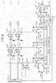
- FIG. 4 is a circuit diagram illustrating the configuration of the first chip 21.
- the first chip 21 includes the light-receiving unit 23, the reading unit 24 (driving unit), the timing generator 25, the buffer 26, and a hysteresis unit 28.
- the hysteresis unit 28 shapes waveforms of the reference clock signal and the synchronization signal input through the transmission cable 3, and outputs, to the timing generator 25, the reference clock signal and the synchronization signal of which the waveforms have been shaped.
- the timing generator 25 generates various driving signals based on the reference clock signal and the synchronization signal input from the hysteresis unit 28, and outputs the driving signals to a vertical scanning unit 241, a noise elimination unit 243, a horizontal scanning unit 245, and a reference voltage generation unit 246 of the reading unit 24 described later, and a first switch 261a, a second switch 261b, and a multiplexer 266 of the buffer 26 described later.
- the reading unit 24 transfers, during periods different from each other, an imaging signal output from each of a plurality of pixels in the light-receiving unit 23 described later, and a reference signal output from a reference signal generation unit.
- the reading unit 24 functions as a transfer unit.
- the reading unit 24 includes the vertical scanning unit 241 (row selection circuit), a current source 242, the noise elimination unit 243, a column source-follower buffer 244 (transistor), the horizontal scanning unit 245 (column selection circuit), the reference voltage generation unit 246, and a reference signal generation unit 248.
- the driving signal such as ⁇ T and ⁇ R
- the noise elimination unit 243 eliminates output variation for each unit pixel 230 and the noise signal at the time of pixel resetting, and outputs an imaging signal photoelectrically converted in each unit pixel 230. Details of the noise elimination unit 243 will be described later.
- a number of unit pixels 230 are disposed in a two-dimensional matrix form.
- Each of the unit pixels 230 includes a photoelectric conversion element 231 (photodiode), a charge converter 233, a transfer transistor 234 (first transfer unit), a pixel resetting unit 236 (transistor), a pixel source-follower transistor 237, and the reference signal generation unit 248.
- one or a plurality of photoelectric conversion elements, and a transfer transistor which transfers a signal charge from each of the photoelectric conversion elements to the charge converter 233 are referred to as a unit cell.
- the unit cell includes a set of one or a plurality of photoelectric conversion elements and the transfer transistor, and each of the unit pixels 230 includes one unit cell.
- the photoelectric conversion element 231 photoelectrically converts incident light to a signal charge in an amount corresponding to the amount of the incident light, and accumulates the signal charge.
- a cathode side of the photoelectric conversion element 231 is connected to one end side of the transfer transistor 234, and an anode side thereof is connected to the ground GND.
- the charge converter 233 is formed of a floating diffusion capacitor (FD), and converts the charge accumulated in the photoelectric conversion element 231 into voltages.
- FD floating diffusion capacitor
- the transfer transistor 234 transfers the charge to the charge converter 233 from the photoelectric conversion element 231.
- a signal line through which a driving signal ⁇ T is supplied is connected, and the other end side thereof is connected to the charge converter 233.
- the transfer transistor 234 is turned to an ON state, and a signal charge is transferred from the photoelectric conversion element 231 to the charge converter 233.
- the pixel resetting unit 236 (transistor) resets the charge converter 233 to a predetermined potential.
- one end side thereof is connected to a variable voltage VR, another end side thereof is connected to the charge converter 233, and to a gate thereof, a signal line through which a driving signal ⁇ R is supplied is connected.
- the driving signal ⁇ R is supplied from the vertical scanning unit 241 through the signal line, the pixel resetting unit 236 is turned to an ON state, and a signal charge accumulated in the charge converter 233 is released to reset the charge converter 233 to a predetermined potential.
- the pixel source-follower transistor 237 (pixel amplifying unit), one end side thereof is connected to the variable voltage VR, and another end side thereof is connected to a vertical transfer line 239.
- a signal subjected to voltage conversion in the charge converter 233 (imaging signal or signal upon resetting) is input.
- the driving signal ⁇ T is supplied to the gate of the transfer transistor 234 after the selection operation described later, a charge is read from the photoelectric conversion element 231, subjected to voltage conversion in the charge converter 233, and then transferred to the vertical transfer line 239 through the pixel source-follower transistor 237.
- the driving signal ⁇ R is supplied to the gate of the pixel resetting unit 236 when the variable voltage VR is at a level of the power supply voltage VDD (for example, 3.3 V)
- VDD for example, 3.3 V
- the pixel source-follower transistor 237 is turned to an ON state, and a unit pixel including the pixel resetting unit 236 is selected (selection operation).
- the driving signal ⁇ R is supplied to the gate of the pixel resetting unit 236 when the variable voltage VR is at a level of deselection voltage Vfd_L (for example, 1 V)
- the pixel source-follower transistor 237 is turned to an OFF state, and the unit pixel including the pixel resetting unit 236 is deselected (deselection operation).
- the reference signal generation unit 248 is connected to a dedicated vertical transfer line 239b, independently from the columns of the unit pixels 230.
- the reference signal generation unit 248 generates a reference signal according to a predetermined voltage, and outputs the signal.
- the reference signal generation unit 248 includes a resetting unit for reference signal generation 236b (transistor), a source-follower transistor for reference signal generation 237b. In other words, it is a configuration obtained by omitting the photoelectric conversion element 231 (photodiode), the charge converter 233, and the transfer transistor 234 (first transfer unit) from the unit pixel 230.
- the resetting unit for reference signal generation 236b fixes a gate of the source-follower transistor for reference signal generation 237b to a predetermined potential.
- one end side thereof is connected to a voltage for reference signal Vfd_H supplied from the reference voltage generation unit 246, another end side thereof is connected to the gate of the source-follower transistor for reference signal generation 237b, and to the gate thereof, a signal line through which a power supply voltage VDD is supplied is connected.
- the resetting unit for reference signal generation 236b consistently fixes the gate of the source-follower transistor for reference signal generation 237b to the voltage Vfd_H.
- one end side thereof is connected to the power supply voltage VDD, and another end side thereof is connected to the vertical transfer line 239b.
- a voltage for a reference signal Vfd_H is input.
- a reference signal in accordance with the voltage for a reference signal Vfd_H black reference signal is consistently transferred to the vertical transfer line 239b through the source-follower transistor for reference signal generation 237b.
- the dedicated vertical transfer line 239b for the reference signal generation unit 248 is the same as the normal vertical transfer line 239 except that the reference signal generation unit 248 is connected thereto instead of a plurality of rows of the unit pixels 230.
- the black reference signal transferred by the vertical transfer line 239b is input to the noise elimination unit 243 in the same manner as for the imaging signal transferred by the vertical transfer line 239.
- a bias voltage Vbias1 is applied in the current source 242 in the current source 242, one end side thereof is connected to the vertical transfer line 239, another end side thereof is connected to the ground GND, and to a gate thereof, a bias voltage Vbias1 is applied.
- the unit pixel 230 and the reference signal generation unit 248 are driven by the current source 242, and an output of the unit pixel 230 (imaging signal) and an output of the reference signal generation unit 248 (black reference signal) are read to the vertical transfer line 239.
- the signals read to the vertical transfer line 239 (imaging signal and black reference signal) are input to the noise elimination unit 243.
- the noise elimination unit 243 includes a transfer capacitor 252 (AC-coupling capacitor) and a clamp switch 253 (transistor).
- a transfer capacitor 252 AC-coupling capacitor
- a clamp switch 253 transistor
- one end side thereof is connected to the vertical transfer line 239, and another end side thereof is connected to the column source-follower buffer 244.
- the clamp switch 253 one end side thereof is connected to a signal line through which a clamp voltage Vclp is supplied from the reference voltage generation unit 246.
- Another end side of the clamp switch 253 is connected to a portion between the transfer capacitor 252 and the column source-follower buffer 244, and to a gate thereof, a driving signal ⁇ VCL is input from the timing generator 25.
- An imaging signal input to the noise elimination unit 243 includes a noise component.
- the clamp switch 253 When the driving signal ⁇ VCL is input to the gate of the clamp switch 253 from the timing generator 25, the clamp switch 253 is turned to an ON state. In accordance therewith, the transfer capacitor 252 is reset by the clamp voltage Vclp supplied from the reference voltage generation unit 246. The black reference signal and the imaging signal of which the noise has been eliminated in the noise elimination unit 243 are input to a gate of the column source-follower buffer 244.
- the noise elimination unit 243 does not need a capacitor for sampling (sampling capacitor), a capacitance of the transfer capacitor 252 (AC-coupling capacitor) only needs to be a capacitance which is sufficient for the input capacitance of the column source-follower buffer 244. In addition, since there is no sampling capacitor, an area occupied by the noise elimination unit 243 in the first chip 21 can be reduced.
- one end side thereof is connected to the power supply voltage VDD, another end side thereof is connected to one end side of a column selection switch 254 (second transfer unit), and to a gate thereof, the imaging signal and the black reference signal are input through the noise elimination unit 243.
- a column selection switch 254 In the column selection switch 254, one end side thereof is connected to another end side of the column source-follower buffer 244, and another end side thereof is connected to a horizontal transfer line 258 (second transfer line).
- a horizontal resetting transistor 256 In a horizontal resetting transistor 256, one end side thereof is connected to a horizontal resetting voltage Vclr, and another end side thereof is connected to the horizontal transfer line 258.
- a driving signal ⁇ HCLR is input from the timing generator 25.
- the horizontal resetting transistor 256 is turned to an ON state, and the horizontal transfer line 258 is reset.
- the column selection switch 254 one end side thereof is connected to another end side of the column source-follower buffer 244, and another end side thereof is connected to the horizontal transfer line (second transfer line) 258.
- a signal line through which a driving signal (column selection pulse) ⁇ HCLK ⁇ N> is supplied from the horizontal scanning unit 245 is connected.
- the driving signal ⁇ HCLK ⁇ N> is supplied to the gate of the column selection switch 254 of a column ⁇ N> from the horizontal scanning unit 245, the column selection switch 254 is turned to an ON state, and signals of the vertical transfer line 239 of the column ⁇ N> (imaging signal and black reference signal) are transferred to the horizontal transfer line 258.
- a constant current source 257 In a constant current source 257, one end side thereof is connected to the horizontal transfer line 258, another end side thereof is connected to the ground GND, and to a gate thereof, a bias voltage Vbias2 is applied.
- the constant current source 257 drives the column source-follower buffer 244, and reads the imaging signal and the black reference signal from the vertical transfer line 239 and the vertical transfer line 239b, respectively, to the horizontal transfer line 258.
- the signals read to the horizontal transfer line 258 are input to the buffer 26 and held therein.
- the reference voltage generation unit 246 generates, based on the signal input from the timing generator 25, the voltage for a reference signal Vfd_H from the power supply voltage VDD and the clamp voltage Vclp of the noise elimination unit 243. A configuration of the reference voltage generation unit 246 will be described in detail with FIGS. 5A and 5B described later.
- the buffer 26 separately holds the imaging signal and the reference signal (black reference signal) input from the horizontal transfer line 258, sequentially switches, based on the signals input from the timing generator 25, between the imaging signal and the reference signal (black reference signal), and outputs the switched signals to the second chip 22.
- the buffer 26 functions as an output unit.
- the buffer 26 includes the first switch 261a, the second switch 261b, a first holding unit 262, a second holding unit 263, a first operational amplifier 264, a second operational amplifier 265, the multiplexer 266, and the output unit 267.
- the first switch 261a one end side thereof is connected to the horizontal transfer line 258 and another end side thereof is connected to an input of the first operational amplifier 264.
- the first switch 261a connects, based on a driving signal ( ⁇ SH1) input from the timing generator 25, the first holding unit 262 and the horizontal transfer line 258.
- the second switch 261b one end side thereof is connected to the horizontal transfer line 258 and another end side thereof is connected to an input of the second operational amplifier 265.
- the second switch 261b connects, based on a driving signal ( ⁇ SH2) input from the timing generator 25, the second holding unit 263 and the horizontal transfer line 258.
- the first holding unit 262 includes a capacitor, and one end side thereof is connected to another end side of the first switch 261a and the input of the first operational amplifier 264, and another end side thereof is connected to the ground. An output of the first operational amplifier 264 is connected to an input of the multiplexer 266.
- the first holding unit 262 holds the reference signal (black reference signal) input through the horizontal transfer line 258, and while the first switch 261a is in an OFF state, outputs the held reference signal (black reference signal) to the multiplexer 266.
- “to hold the reference signal (black reference signal)” means “to hold an amount of charge corresponding to a signal level (voltage) of the reference signal”.
- a capacitance C1 of the first holding unit 262 is larger than a capacitance C2 of the second holding unit 263 (C1 > C2).
- the second holding unit 263 includes a capacitor, and one end side thereof is connected to another end side of the second switch 261b and the input of the second operational amplifier 265, and another end side thereof is connected to the ground. An output of the second operational amplifier 265 is connected to the input of the multiplexer 266.
- the second holding unit 263 holds the imaging signal input through the horizontal transfer line 258, and while the second switch 261b is in an OFF state, outputs the held imaging signal to the multiplexer 266.
- “to hold the imaging signal” means “to hold an amount of charge corresponding to the imaging signal”.
- the multiplexer 266 is driven by a driving signal ( ⁇ MUXSEL) supplied from the timing generator 25, sequentially switches between the reference signal (black reference signal) input from the first holding unit 262 and the imaging signal input from the second holding unit 263, and outputs the switched signals to the second chip 22 through the output unit 267 (amplifier). In that sense, the multiplexer 266 functions as a switching unit in the first embodiment.
- a pulsed driving signal ( ⁇ MUXSEL: High) is output from the timing generator 25, the multiplexer 266 outputs the imaging signal input from the second holding unit 263 to the second chip 22.
- the output unit 267 performs, if necessary, signal amplification on the imaging signal whose noise has been eliminated and a reference voltage Vref, and outputs the imaging signal and the reference voltage alternately to the second chip 22.
- the second chip 22 transmits only an alternating-current component of the imaging signal whose noise has been eliminated and the reference voltage Vref, to the connector unit 5 through the transmission cable 3.
- FIGS. 5A and 5B are circuit diagrams illustrating the configuration of the reference voltage generation unit 246.
- a reference voltage generation unit 246a illustrated in FIG. 5A includes a resistance voltage divider circuit including two resistors 291 and 292, and a multiplexer 293 driven by a driving signal ⁇ VRSEL.
- the multiplexer 293 alternately switches between the power supply voltage VDD and the deselection voltage Vfd_L generated in the resistance voltage divider circuit, and applies the switched voltages as the variable voltage VR to all pixels and the reference signal generation unit 248.
- a reference voltage generation unit 246b illustrated in FIG. 5B includes a resistance voltage divider circuit including two resistors 291 and 292, and a switch 294 (transistor) driven by a driving signal ⁇ VSH.
- the reference voltage generation unit 246b generates, at the timing when the driving signal ⁇ VSH is driven by the driving of the switch 294, the voltage for a reference signal Vfd_H and the clamp voltage Vclp of the noise elimination unit 243 from the power supply voltage VDD.
- FIG. 6 is a timing chart illustrating the drive timing of the imaging unit 20.
- FIG. 7 is a timing chart illustrating an enlarged region F1 of FIG. 6 .
- the variable voltage VR, the driving signal ⁇ VSH, and driving signals ⁇ R, ⁇ T, ⁇ VCL, ⁇ Hdmy, ⁇ HCLK, ⁇ HCLR, ⁇ SH1, ⁇ SH2, and ⁇ MUXSEL are illustrated sequentially from the top.
- the driving signals ⁇ R and ⁇ T are signals in cases where the row ⁇ M> is ⁇ 0> and ⁇ 1>
- the driving signal ⁇ HCLK is a signal in cases where the column ⁇ N> is ⁇ 1> and ⁇ 2>.
- the variable voltage VR is adjusted to be a VDD level (for example, 3.3 V).
- a driving signal ⁇ R ⁇ 0> is applied in a pulsed manner to a gate of the pixel resetting unit 236 of a pixel row ⁇ 0>. Consequently, the power supply voltage VDD is applied to a gate of the pixel source-follower transistor 237 of the pixel row ⁇ 0>, and the pixel source-follower transistor 237 is turned to an ON state.
- the unit pixel 230 included in the pixel row ⁇ 0> is selected (selection operation).
- a noise signal is output to the vertical transfer line 239 from the unit pixel 230.
- the noise signal includes fluctuations unique to the unit pixel 230 to be read, a noise upon pixel resetting, and the like.
- a voltage of a gate of the column source-follower buffer 244 is adjusted to be the clamp voltage Vclp by making a transition of the clamp switch 253 from an ON state ( ⁇ VCL: High) to an OFF state ( ⁇ VCL: Low).
- the clamp voltage Vclp is determined at a falling timing of ⁇ VSH.
- a signal which is obtained by converting, by the charge converter 233, the charge photoelectrically converted by the photoelectric conversion element 231, is read to the vertical transfer line 239.
- an imaging signal optical signal obtained by subtracting the noise signal is output to the gate of the column source-follower buffer 244 through the transfer capacitor 252.
- the signal output to the gate of the column source-follower buffer 244 is a signal sampled based on the clamp voltage Vclp as a reference.
- the horizontal resetting transistor 256 After sampling a black reference signal based on the clamp voltage Vclp as a reference, the horizontal resetting transistor 256 is turned to an OFF state ( ⁇ HCLR: Low) to cancel the resetting of the horizontal transfer line 258, and the column selection switch 254 provided on the most downstream side of a vertical transfer line 239a is turned to an ON state ( ⁇ Hdmy: High). By doing so, the black reference signal is transferred to the horizontal transfer line 258. Thereafter, by turning the first switch 261a to an ON state ( ⁇ SH1: High), the reference signal (black reference signal) is sampled by the first holding unit 262 and held therein.
- ⁇ HCLR Low
- ⁇ Hdmy High
- the first switch 261a is turned to an OFF state ( ⁇ SH1: Low), and the column selection switch 254 at the most downstream side is turned to an OFF state ( ⁇ Hdmy: Low).
- a period during which the first switch 261a is in the ON state (sampling period) is shorter than a period during which the column selection switch 254 at the most downstream side is in the ON state (transfer period).
- the horizontal resetting transistor 256 is turned to an ON state ( ⁇ HCLR: High) in a pulsed manner to reset the horizontal transfer line 258 again.
- a driving signal is not output to the multiplexer 266 ( ⁇ MUXSEL: Low). Therefore, the multiplexer 266 outputs the reference signal (black reference signal) held by the first holding unit 262 to the output unit 267.
- a series of operations performed after the transfer transistor 234 has been turned to the ON state ( ⁇ T ⁇ 0>: High) in a pulsed manner in other words, a series of operations including from the operation for turning the horizontal resetting transistor 256 to the OFF state ( ⁇ HCLR: Low) to the operation for outputting the reference signal (black reference signal) to the output unit 267, is repeated a predetermined number of times (in FIGS. 6 and 7 , twice).
- the reference signal black reference signal
- the reference signal black reference signal
- the number of times of repeating the series of operations can be reduced to, approximately, two to ten.
- the multiplexer 266 outputs the imaging signal held in the second holding unit 263 to the output unit 267.
- the horizontal resetting transistor 256 is turned to an ON state ( ⁇ HCLR: High) in a pulsed manner to reset the horizontal transfer line 258 again. While the horizontal resetting transistor 256 is in the ON state, the output of the driving signal to the multiplexer 266 ends ( ⁇ MUXSEL: Low). Thereafter, the horizontal resetting transistor 256 is turned to an OFF state ( ⁇ HCLR: Low) .
- an imaging signal of the column ⁇ 2> is transferred to the horizontal transfer line 258.
- the second switch 261b is turned to the ON state ( ⁇ SH2: High)
- the imaging signal is sampled by the second holding unit 263 and held therein.
- the second switch 261b is turned to the OFF state ( ⁇ SH2: Low)
- the column selection switch 254 of the column ⁇ 2> is turned to an OFF state ( ⁇ HCLK ⁇ 2>: Low).
- the multiplexer 266 performs an operation to output the imaging signal held in the second holding unit 263 to the output unit 267. The operation is the same as the operation to output the imaging signal described for the column ⁇ 1>.
- the imaging unit 20 repeats the operations for each column as many times as the number of columns of the light-receiving unit 23 (or the number of columns required to read), thereby outputting the imaging signals for one line.
- the variable voltage VR is adjusted to be a Vfd_L level (for example, 1 V).
- the driving signal ⁇ R ⁇ 0> is applied in a pulsed manner to a gate of the pixel resetting unit 236 of the selected pixel row ⁇ 0>. Consequently, the deselection voltage Vfd_L is applied to the gate of the pixel source-follower transistor 237 of the pixel row ⁇ 0>, and the pixel source-follower transistor 237 is turned to an OFF state.
- the unit pixel 230 included in the pixel row ⁇ 0> is deselected (deselection operation).
- imaging signals for one frame are output.
- a black reference signal is positioned at the head of signal output of each row.
- a black reference signal corresponding to a plurality of columns is temporarily stored and subjected to averaging in the imaging signal processing unit 52. Thereafter, a noise component is extracted therefrom, and the extracted noise component is used for eliminating a noise component included in the imaging signal.
- the buffer 26 separately holds the reference signal and the imaging signal, sequentially switches between the signals and outputs the switched signals, whereby a read time of an OB region can be shortened. As a result, a frame rate of the imaging signal can be improved.
- the read time of the OB region can be shortened. Consequently, in a case where the image sensor (first chip 21) includes CMOS, distortion of an image caused by a rolling shutter can be reduced.
- the reading unit 24 reads each of the reference signal generated by the reference signal generation unit 248 and the imaging signal generated by the unit pixel 230, whereby each of the reference signal and the imaging signal changes in the same manner even when there is a variation in the signals upon manufacturing. Therefore, the imaging signal can be accurately corrected based on the reference signal. As a result, improvement in image quality can be realized.
- the reference signal generation unit 248 without a photoelectric conversion element 231 (photodiode) is provided independently from the columns of the unit pixel 230, and the black reference signal is read only a predetermined number of times (two or more times) from the reference signal generation unit 248 before reading a signal of each row of the unit pixel 230. Therefore, the black reference signal corresponding to a plurality of columns is positioned at the head of the signals of each row.
- the black reference signal on the side of the imaging signal processing unit 52 reduction of horizontal lines or the like can be performed. Therefore, improvement in image quality can be realized.
- the reference signal generation unit 248 is not provided with the photoelectric conversion element 231. Therefore, there is no need to provide a light shielding sheet or the like to output the black reference signal. Furthermore, since the reference signal generation unit 248 does not originally have a configuration which responds to light, there is no need to provide the reference signal generation unit 248 over a plurality of columns in order to eliminate an influence of the leakage of light. Therefore, size reduction of the imaging unit 20 can be realized as well as improvement in image quality.
- the imaging unit 20 transmits the black reference signal generated by the reference signal generation unit 248 to the connector unit 5 when moving from a horizontal blanking period to an imaging signal period, occurrence of fluctuations in the power supply voltage, which is caused by fluctuations in power consumption, can be suppressed. Therefore, deterioration of the image quality caused by fluctuations in the power supply can be suppressed.
- the reference signal generation unit 248 is provided on the first vertical line in the light-receiving unit 23.
- the reference signal generation unit 248 may be provided, for example, on the last vertical line in the light-receiving unit 23.
- An endoscope system according to the second embodiment has a similar configuration to the endoscope system 1 according to the first embodiment, and is different from the first embodiment in a configuration of a first chip of an imaging unit (imaging device) and an operation of the imaging unit. Therefore, hereinbelow, the configuration of the first chip in the imaging unit according to the second embodiment will be described, and then the operation of the imaging unit will be described.
- the same reference signs are given to the same elements as those of the endoscope system 1 according to the first embodiment, and the explanation thereof will be omitted.
- FIG. 8 is a block diagram illustrating a detailed configuration of a first chip 21a in an imaging unit 20a according to the second embodiment.
- FIG. 9 is a circuit diagram illustrating the configuration of the first chip 21a.
- the first chip 21a includes a light-receiving unit 23, a reading unit 24 (driving unit), a timing generator 25, a buffer 26a, and a hysteresis unit 28.
- the buffer 26a includes a sample holding switch 261, a first holding unit 262, a second holding unit 263, a first operational amplifier 264, a second operational amplifier 265, a multiplexer 266, an output unit 267, and a resetting unit 268.
- the resetting unit 268 is provided between the second holding unit 263 and the multiplexer 266, and resets the second holding unit 263 after the multiplexer 266 has output the reference signal held by the first holding unit 262.
- the resetting operation is also referred to as "to reset a voltage of the second holding unit 263 to the reference voltage Vref".
- FIG. 10 is a timing chart illustrating the drive timing of the imaging unit 20a.
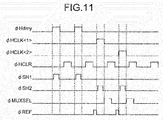
- FIG. 11 is a timing chart illustrating an enlarged region F2 of FIG. 10 .
- a variable voltage VR, a driving signal ⁇ VSH, and driving signals ⁇ R, ⁇ T, ⁇ VCL, ⁇ Hdmy, ⁇ HCLK, ⁇ HCLR, ⁇ SH1, ⁇ SH2, ⁇ MUXSEL, and ⁇ REF are illustrated sequentially from the top.
- the driving signals ⁇ R and ⁇ T are signals in cases where the row ⁇ M> is ⁇ 0> and ⁇ 1>, and the driving signal ⁇ HCLK is a signal in cases where the column ⁇ N> is ⁇ 1> and ⁇ 2>.
- the operations which are performed by the imaging unit 20a and include from the operation for setting the variable voltage VR to the operations for reading the reference signal (black reference signal) a predetermined number of times (in FIGS. 10 and 11 , twice) and outputting the signal, are the same as those described in the first embodiment (see, FIG. 6 ).
- the imaging unit 20a reads the reference signal (black reference signal) a predetermined number of times and outputs the signal, then turns the resetting unit 268 to an ON state ( ⁇ REF: High), and resets the voltage of the second holding unit 263 to the reference voltage Vref. Subsequently, the imaging unit 20a performs an operation for reading and outputting an imaging signal of a column ⁇ 1> in the same manner as in the first embodiment.
- the imaging unit 20a sequentially performs the operation for the column ⁇ 1> described above with respective to all columns required to read, thereby outputting the imaging signals for one line. Thereafter, the imaging unit 20a performs a deselection operation of a unit pixel 230 included in a pixel row ⁇ 0>.
- imaging signals for one frame are output.
- a black reference signal is positioned at the head of signal output of each row.
- the black reference signal is used to eliminate a noise component included in the imaging signal, which is the same as the case of the first embodiment.
- the buffer 26a separately holds the reference signal and the imaging signal, sequentially switches between the signals and outputs the switched signals, whereby a read time of an OB region can be shortened. As a result, a frame rate can be improved.
- noiseless imaging signals can be sequentially output.
- the present invention may include various embodiments not described herein, and various design changes and the like can be performed in the scope of technical ideas specified by the claims.
Landscapes
- Health & Medical Sciences (AREA)
- Life Sciences & Earth Sciences (AREA)
- Engineering & Computer Science (AREA)
- Surgery (AREA)
- Signal Processing (AREA)
- Multimedia (AREA)
- Radiology & Medical Imaging (AREA)
- Molecular Biology (AREA)
- Optics & Photonics (AREA)
- Pathology (AREA)
- Biophysics (AREA)
- Physics & Mathematics (AREA)
- Biomedical Technology (AREA)
- Heart & Thoracic Surgery (AREA)
- Medical Informatics (AREA)
- Nuclear Medicine, Radiotherapy & Molecular Imaging (AREA)
- Animal Behavior & Ethology (AREA)
- General Health & Medical Sciences (AREA)
- Public Health (AREA)
- Veterinary Medicine (AREA)
- Transforming Light Signals Into Electric Signals (AREA)
- Endoscopes (AREA)
- Solid State Image Pick-Up Elements (AREA)
Claims (8)
- Bildsensor (21), umfassend:eine Mehrzahl von Pixeln (230), die in einer zweidimensionalen Matrixform angeordnet sind und dazu konfiguriert sind, Licht von außen aufzunehmen, entsprechende Bildgebungssignale gemäß eines Umfangs des aufgenommenen Lichts zu erzeugen und die Bildgebungssignale an entsprechende einer Mehrzahl von vertikalen Übertragungsleitungen (239) auszugeben;eine Referenzsignalerzeugungseinheit (248), die dazu konfiguriert ist, ein Referenzsignal gemäß einer vorbestimmten Spannung zu erzeugen und das Referenzsignal an eine dedizierte vertikale Übertragungsleitung (239b) auszugeben, die separat von der Mehrzahl von vertikalen Übertragungsleitungen (239) vorgesehen ist,gekennzeichnet durch weiterhin umfassend:eine Übertragungseinheit (24), die dazu konfiguriert ist, sequentiell das Referenzsignal von der dedizierten vertikalen Übertragungsleitung (239b) und die Bildgebungssignale von den entsprechenden der Mehrzahl von vertikalen Übertragungsleitungen (239) an eine horizontale Übertragungsleitung (258) während unterschiedlichen Übertragungsperioden für jede Reihe der zweidimensionalen Matrix zu übertragen; undeine Ausgabeeinheit (267), die dazu konfiguriert ist, das Referenzsignal und die Bildgebungssignale von der horizontalen Übertragungsleitung (258) einzugeben,wobei die Ausgabeeinheit (267) umfasst:eine erste Halteeinheit (262), die dazu konfiguriert ist, das Referenzsignal zu halten;eine zweite Halteeinheit (263), die dazu konfiguriert ist, sequentiell die Bildgebungssignale zu halten; undeine Schalteinheit (266), die mit jeder der ersten Halteeinheit (262) und der zweiten Halteeinheit (263) verbunden ist und dazu konfiguriert ist, sequentiell zwischen dem von der ersten Halteeinheit (262) gehaltenen Referenzsignal und dem von der zweiten Halteeinheit (263) gehaltenen Bildgebungssignal zu schalten, um ein Schaltsignal für jedes Bildgebungssignal auszugeben.
- Bildsensor (21) nach Anspruch 1, weiterhin umfassend eine Rückstelleinheit (268), die zwischen der zweiten Halteeinheit (263) und der Schalteinheit (266) vorgesehen ist und dazu konfiguriert ist, die erste Halteeinheit (262) zurückzustellen, nachdem die Schalteinheit (266) das von der ersten Halteeinheit (262) gehaltene Referenzsignal ausgegeben hat.
- Bildsensor (21) nach Anspruch 1, wobei eine Kapazitanz der ersten Halteeinheit (262) größer als eine Kapazitanz der zweiten Halteeinheit (263) ist.
- Bildsensor (21) nach Anspruch 1, wobei das Referenzsignal ein schwarzes Referenzsignal zum Bestimmen eines Schwarzwerts des Bildgebungssignals ist.
- Bildsensor (21) nach Anspruch 1, wobei
die Referenzsignalerzeugungseinheit (248) dazu konfiguriert ist, das Referenzsignal für jede Leitung (239, 239b) zu erzeugen, und
die Schalteinheit (266) dazu konfiguriert ist, zwischen dem Referenzsignal und dem Bildgebungssignal für jedes Pixel (230) zu schalten, um das Schaltsignal auszugeben. - Bildgebungsvorrichtung (20), die den Bildsensor (21) nach Anspruch 1 umfasst.
- Endoskop (2), das die Bildgebungsvorrichtung (20) nach Anspruch 6 an einer distalen Endseite einer Einführungseinheit des Endoskops (2) umfasst.
- Endoskopsystem (1), umfassend:das Endoskop (2) nach Anspruch 7 undeine Verarbeitungsvorrichtung (6), die dazu konfiguriert ist, ein Bildgebungssignal in ein Bildsignal umzuwandeln.
Applications Claiming Priority (2)
| Application Number | Priority Date | Filing Date | Title |
|---|---|---|---|
| JP2014137103 | 2014-07-02 | ||
| PCT/JP2015/056678 WO2016002257A1 (ja) | 2014-07-02 | 2015-03-06 | 撮像素子、撮像装置、内視鏡、内視鏡システムおよび撮像素子の駆動方法 |
Publications (3)
| Publication Number | Publication Date |
|---|---|
| EP3157248A1 EP3157248A1 (de) | 2017-04-19 |
| EP3157248A4 EP3157248A4 (de) | 2018-02-21 |
| EP3157248B1 true EP3157248B1 (de) | 2019-05-08 |
Family
ID=55018820
Family Applications (1)
| Application Number | Title | Priority Date | Filing Date |
|---|---|---|---|
| EP15814044.2A Active EP3157248B1 (de) | 2014-07-02 | 2015-03-06 | Bildgebungselement, bildgebungsvorrichtung, endoskop, endoskopsystem und verfahren zur ansteuerung eines bildgebungselements |
Country Status (5)
| Country | Link |
|---|---|
| US (1) | US9974431B2 (de) |
| EP (1) | EP3157248B1 (de) |
| JP (1) | JP5861012B1 (de) |
| CN (1) | CN105637857B (de) |
| WO (1) | WO2016002257A1 (de) |
Families Citing this family (8)
| Publication number | Priority date | Publication date | Assignee | Title |
|---|---|---|---|---|
| EP3127466B1 (de) * | 2014-03-31 | 2018-08-22 | Fujifilm Corporation | Endoskopsystem, verarbeitungsvorrichtung des endoskopsystems und verfahren zum betrieb des endoskopsystems |
| WO2016088422A1 (ja) * | 2014-12-04 | 2016-06-09 | オリンパス株式会社 | 内視鏡 |
| CN109983762B (zh) * | 2017-01-17 | 2021-06-01 | 奥林巴斯株式会社 | 摄像装置和内窥镜系统 |
| US11633089B2 (en) | 2019-06-20 | 2023-04-25 | Cilag Gmbh International | Fluorescence imaging with minimal area monolithic image sensor |
| US11432706B2 (en) | 2019-06-20 | 2022-09-06 | Cilag Gmbh International | Hyperspectral imaging with minimal area monolithic image sensor |
| US10952619B2 (en) | 2019-06-20 | 2021-03-23 | Ethicon Llc | Hyperspectral and fluorescence imaging and topology laser mapping with minimal area monolithic image sensor |
| US10841504B1 (en) | 2019-06-20 | 2020-11-17 | Ethicon Llc | Fluorescence imaging with minimal area monolithic image sensor |
| CN111263052B (zh) * | 2020-03-27 | 2024-12-17 | 深圳市华尔视通科技有限公司 | 一种双摄像头内窥镜切换电路及其设备 |
Family Cites Families (35)
| Publication number | Priority date | Publication date | Assignee | Title |
|---|---|---|---|---|
| JP2806035B2 (ja) * | 1990-11-26 | 1998-09-30 | 日本電気株式会社 | 映像信号処理回路 |
| JP3697769B2 (ja) * | 1995-02-24 | 2005-09-21 | 株式会社ニコン | 光電変換素子及び光電変換装置 |
| US5677527A (en) * | 1995-10-11 | 1997-10-14 | Must Systems, Inc. | Compensation method and apparatus for image signals generated by CCD |
| JP4681767B2 (ja) * | 2001-07-17 | 2011-05-11 | キヤノン株式会社 | 撮像装置およびカメラ |
| US7084912B2 (en) * | 2001-09-20 | 2006-08-01 | Yuen-Shung Chieh | Method for reducing coherent row-wise and column-wise fixed pattern noise in CMOS image sensors |
| JP4355148B2 (ja) * | 2003-02-28 | 2009-10-28 | パナソニック株式会社 | 固体撮像装置の駆動方法 |
| TWI259661B (en) * | 2004-01-08 | 2006-08-01 | Novatek Microelectronics Corp | Analog front end circuit and method thereof |
| JP4479373B2 (ja) * | 2004-06-28 | 2010-06-09 | ソニー株式会社 | イメージセンサ |
| US7372493B2 (en) * | 2004-07-12 | 2008-05-13 | Micron Technology, Inc. | Column-wise clamp voltage driver for suppression of noise in an imager |
| WO2008150283A1 (en) * | 2007-05-21 | 2008-12-11 | Micron Technology, Inc. | Suppression of row-wise noise in cmos image sensors |
| JP4353281B2 (ja) * | 2007-06-06 | 2009-10-28 | ソニー株式会社 | A/d変換回路、a/d変換回路の制御方法、固体撮像装置および撮像装置 |
| JP5098502B2 (ja) * | 2007-08-08 | 2012-12-12 | 株式会社ニコン | 固体撮像装置 |
| JP5268454B2 (ja) * | 2007-08-09 | 2013-08-21 | キヤノン株式会社 | 撮像装置 |
| JP4367963B2 (ja) | 2007-10-24 | 2009-11-18 | キヤノン株式会社 | 撮像装置、撮像システム、及び撮像装置の駆動方法 |
| JP5053869B2 (ja) * | 2008-01-10 | 2012-10-24 | キヤノン株式会社 | 固体撮像装置、撮像システム、及び固体撮像装置の駆動方法 |
| JP2009272909A (ja) * | 2008-05-08 | 2009-11-19 | Hoya Corp | デジタル映像信号送信装置、受信装置およびシステム |
| JP2010147948A (ja) * | 2008-12-19 | 2010-07-01 | Canon Inc | 撮像装置及び撮像システム |
| JP2011029793A (ja) * | 2009-07-22 | 2011-02-10 | Panasonic Corp | 固体撮像装置およびカメラ |
| JP5495701B2 (ja) * | 2009-10-07 | 2014-05-21 | キヤノン株式会社 | 固体撮像装置 |
| JP2011109584A (ja) * | 2009-11-20 | 2011-06-02 | Panasonic Corp | 固体撮像素子および固体撮像装置 |
| GB2479594A (en) * | 2010-04-16 | 2011-10-19 | St Microelectronics | A sample and hold circuit with internal averaging of samples |
| JP5632660B2 (ja) * | 2010-06-18 | 2014-11-26 | キヤノン株式会社 | Ad変換器及びそれを複数用いた固体撮像装置 |
| JP5534997B2 (ja) * | 2010-08-03 | 2014-07-02 | 富士フイルム株式会社 | 電子内視鏡システム |
| JP5906596B2 (ja) * | 2010-08-16 | 2016-04-20 | 株式会社ニコン | 撮像装置 |
| JP5693146B2 (ja) * | 2010-10-29 | 2015-04-01 | キヤノン株式会社 | 固体撮像装置及び固体撮像装置の駆動方法 |
| US8730364B2 (en) * | 2010-11-09 | 2014-05-20 | Omnivision Technologies, Inc. | Image sensor with pipelined column analog-to-digital converters |
| JP2012119956A (ja) * | 2010-12-01 | 2012-06-21 | Fujifilm Corp | 放射線画像検出装置 |
| US8405747B2 (en) * | 2011-02-17 | 2013-03-26 | Omnivision Technologies, Inc. | Analog row black level calibration for CMOS image sensor |
| JP2012235193A (ja) * | 2011-04-28 | 2012-11-29 | Canon Inc | 撮像素子、撮像装置、およびその制御方法、並びに制御プログラム |
| JP5933219B2 (ja) * | 2011-10-21 | 2016-06-08 | オリンパス株式会社 | 固体撮像装置 |
| WO2013088644A1 (ja) * | 2011-12-14 | 2013-06-20 | パナソニック株式会社 | 固体撮像装置及び撮像装置 |
| JP6103934B2 (ja) * | 2012-12-28 | 2017-03-29 | キヤノン株式会社 | 光電変換装置、撮像システム、および光電変換装置の駆動方法 |
| WO2014115390A1 (ja) * | 2013-01-23 | 2014-07-31 | オリンパスメディカルシステムズ株式会社 | 撮像装置、内視鏡システム及びノイズ除去方法 |
| JP2015080132A (ja) * | 2013-10-18 | 2015-04-23 | ルネサスエレクトロニクス株式会社 | 固体撮像素子 |
| JP6175355B2 (ja) * | 2013-11-07 | 2017-08-02 | ルネサスエレクトロニクス株式会社 | 固体撮像素子 |
-
2015
- 2015-03-06 EP EP15814044.2A patent/EP3157248B1/de active Active
- 2015-03-06 WO PCT/JP2015/056678 patent/WO2016002257A1/ja not_active Ceased
- 2015-03-06 CN CN201580002235.7A patent/CN105637857B/zh active Active
- 2015-03-06 JP JP2015534870A patent/JP5861012B1/ja active Active
-
2016
- 2016-04-05 US US15/090,905 patent/US9974431B2/en active Active
Non-Patent Citations (1)
| Title |
|---|
| None * |
Also Published As
| Publication number | Publication date |
|---|---|
| CN105637857A (zh) | 2016-06-01 |
| JPWO2016002257A1 (ja) | 2017-04-27 |
| EP3157248A1 (de) | 2017-04-19 |
| US9974431B2 (en) | 2018-05-22 |
| JP5861012B1 (ja) | 2016-02-16 |
| WO2016002257A1 (ja) | 2016-01-07 |
| CN105637857B (zh) | 2019-06-07 |
| US20160213238A1 (en) | 2016-07-28 |
| EP3157248A4 (de) | 2018-02-21 |
Similar Documents
| Publication | Publication Date | Title |
|---|---|---|
| EP3157248B1 (de) | Bildgebungselement, bildgebungsvorrichtung, endoskop, endoskopsystem und verfahren zur ansteuerung eines bildgebungselements | |
| JP5826968B2 (ja) | 撮像素子、撮像装置、内視鏡および内視鏡システム | |
| CN104303495B (zh) | 摄像装置、内窥镜系统以及噪声去除方法 | |
| EP2988492B1 (de) | Bildaufnahmeelement, bildaufnahmevorrichtung und endoskopsystem | |
| US9813645B2 (en) | Image sensor, imaging device, endoscope, and endoscopic system | |
| US10638068B2 (en) | Endoscope and endoscope system | |
| US20180054580A1 (en) | Image sensor and endoscope | |
| US9693002B2 (en) | Image sensor, imaging device, endoscope, and endoscope system | |
| US20180035868A1 (en) | Imaging device, endoscope, and endoscope system | |
| US20170311787A1 (en) | Image sensor and endoscope | |
| JPWO2014175006A1 (ja) | 撮像素子、撮像装置、内視鏡および内視鏡システム | |
| JP6313912B2 (ja) | 撮像素子、内視鏡および内視鏡システム | |
| JP2017123971A (ja) | 内視鏡 |
Legal Events
| Date | Code | Title | Description |
|---|---|---|---|
| STAA | Information on the status of an ep patent application or granted ep patent |
Free format text: STATUS: THE INTERNATIONAL PUBLICATION HAS BEEN MADE |
|
| PUAI | Public reference made under article 153(3) epc to a published international application that has entered the european phase |
Free format text: ORIGINAL CODE: 0009012 |
|
| STAA | Information on the status of an ep patent application or granted ep patent |
Free format text: STATUS: REQUEST FOR EXAMINATION WAS MADE |
|
| 17P | Request for examination filed |
Effective date: 20170113 |
|
| AK | Designated contracting states |
Kind code of ref document: A1 Designated state(s): AL AT BE BG CH CY CZ DE DK EE ES FI FR GB GR HR HU IE IS IT LI LT LU LV MC MK MT NL NO PL PT RO RS SE SI SK SM TR |
|
| AX | Request for extension of the european patent |
Extension state: BA ME |
|
| DAV | Request for validation of the european patent (deleted) | ||
| DAX | Request for extension of the european patent (deleted) | ||
| A4 | Supplementary search report drawn up and despatched |
Effective date: 20180123 |
|
| RIC1 | Information provided on ipc code assigned before grant |
Ipc: H04N 5/361 20110101AFI20180118BHEP Ipc: H04N 5/376 20110101ALI20180118BHEP |
|
| GRAP | Despatch of communication of intention to grant a patent |
Free format text: ORIGINAL CODE: EPIDOSNIGR1 |
|
| STAA | Information on the status of an ep patent application or granted ep patent |
Free format text: STATUS: GRANT OF PATENT IS INTENDED |
|
| INTG | Intention to grant announced |
Effective date: 20181016 |
|
| GRAS | Grant fee paid |
Free format text: ORIGINAL CODE: EPIDOSNIGR3 |
|
| GRAA | (expected) grant |
Free format text: ORIGINAL CODE: 0009210 |
|
| STAA | Information on the status of an ep patent application or granted ep patent |
Free format text: STATUS: THE PATENT HAS BEEN GRANTED |
|
| AK | Designated contracting states |
Kind code of ref document: B1 Designated state(s): AL AT BE BG CH CY CZ DE DK EE ES FI FR GB GR HR HU IE IS IT LI LT LU LV MC MK MT NL NO PL PT RO RS SE SI SK SM TR |
|
| REG | Reference to a national code |
Ref country code: GB Ref legal event code: FG4D |
|
| REG | Reference to a national code |
Ref country code: CH Ref legal event code: EP Ref country code: AT Ref legal event code: REF Ref document number: 1132054 Country of ref document: AT Kind code of ref document: T Effective date: 20190515 |
|
| REG | Reference to a national code |
Ref country code: DE Ref legal event code: R096 Ref document number: 602015030051 Country of ref document: DE Ref country code: IE Ref legal event code: FG4D |
|
| REG | Reference to a national code |
Ref country code: NL Ref legal event code: MP Effective date: 20190508 |
|
| REG | Reference to a national code |
Ref country code: LT Ref legal event code: MG4D |
|
| PG25 | Lapsed in a contracting state [announced via postgrant information from national office to epo] |
Ref country code: FI Free format text: LAPSE BECAUSE OF FAILURE TO SUBMIT A TRANSLATION OF THE DESCRIPTION OR TO PAY THE FEE WITHIN THE PRESCRIBED TIME-LIMIT Effective date: 20190508 Ref country code: NO Free format text: LAPSE BECAUSE OF FAILURE TO SUBMIT A TRANSLATION OF THE DESCRIPTION OR TO PAY THE FEE WITHIN THE PRESCRIBED TIME-LIMIT Effective date: 20190808 Ref country code: HR Free format text: LAPSE BECAUSE OF FAILURE TO SUBMIT A TRANSLATION OF THE DESCRIPTION OR TO PAY THE FEE WITHIN THE PRESCRIBED TIME-LIMIT Effective date: 20190508 Ref country code: AL Free format text: LAPSE BECAUSE OF FAILURE TO SUBMIT A TRANSLATION OF THE DESCRIPTION OR TO PAY THE FEE WITHIN THE PRESCRIBED TIME-LIMIT Effective date: 20190508 Ref country code: SE Free format text: LAPSE BECAUSE OF FAILURE TO SUBMIT A TRANSLATION OF THE DESCRIPTION OR TO PAY THE FEE WITHIN THE PRESCRIBED TIME-LIMIT Effective date: 20190508 Ref country code: PT Free format text: LAPSE BECAUSE OF FAILURE TO SUBMIT A TRANSLATION OF THE DESCRIPTION OR TO PAY THE FEE WITHIN THE PRESCRIBED TIME-LIMIT Effective date: 20190908 Ref country code: ES Free format text: LAPSE BECAUSE OF FAILURE TO SUBMIT A TRANSLATION OF THE DESCRIPTION OR TO PAY THE FEE WITHIN THE PRESCRIBED TIME-LIMIT Effective date: 20190508 Ref country code: LT Free format text: LAPSE BECAUSE OF FAILURE TO SUBMIT A TRANSLATION OF THE DESCRIPTION OR TO PAY THE FEE WITHIN THE PRESCRIBED TIME-LIMIT Effective date: 20190508 Ref country code: NL Free format text: LAPSE BECAUSE OF FAILURE TO SUBMIT A TRANSLATION OF THE DESCRIPTION OR TO PAY THE FEE WITHIN THE PRESCRIBED TIME-LIMIT Effective date: 20190508 |
|
| PG25 | Lapsed in a contracting state [announced via postgrant information from national office to epo] |
Ref country code: BG Free format text: LAPSE BECAUSE OF FAILURE TO SUBMIT A TRANSLATION OF THE DESCRIPTION OR TO PAY THE FEE WITHIN THE PRESCRIBED TIME-LIMIT Effective date: 20190808 Ref country code: RS Free format text: LAPSE BECAUSE OF FAILURE TO SUBMIT A TRANSLATION OF THE DESCRIPTION OR TO PAY THE FEE WITHIN THE PRESCRIBED TIME-LIMIT Effective date: 20190508 Ref country code: LV Free format text: LAPSE BECAUSE OF FAILURE TO SUBMIT A TRANSLATION OF THE DESCRIPTION OR TO PAY THE FEE WITHIN THE PRESCRIBED TIME-LIMIT Effective date: 20190508 Ref country code: GR Free format text: LAPSE BECAUSE OF FAILURE TO SUBMIT A TRANSLATION OF THE DESCRIPTION OR TO PAY THE FEE WITHIN THE PRESCRIBED TIME-LIMIT Effective date: 20190809 |
|
| REG | Reference to a national code |
Ref country code: AT Ref legal event code: MK05 Ref document number: 1132054 Country of ref document: AT Kind code of ref document: T Effective date: 20190508 |
|
| PG25 | Lapsed in a contracting state [announced via postgrant information from national office to epo] |
Ref country code: SK Free format text: LAPSE BECAUSE OF FAILURE TO SUBMIT A TRANSLATION OF THE DESCRIPTION OR TO PAY THE FEE WITHIN THE PRESCRIBED TIME-LIMIT Effective date: 20190508 Ref country code: RO Free format text: LAPSE BECAUSE OF FAILURE TO SUBMIT A TRANSLATION OF THE DESCRIPTION OR TO PAY THE FEE WITHIN THE PRESCRIBED TIME-LIMIT Effective date: 20190508 Ref country code: EE Free format text: LAPSE BECAUSE OF FAILURE TO SUBMIT A TRANSLATION OF THE DESCRIPTION OR TO PAY THE FEE WITHIN THE PRESCRIBED TIME-LIMIT Effective date: 20190508 Ref country code: DK Free format text: LAPSE BECAUSE OF FAILURE TO SUBMIT A TRANSLATION OF THE DESCRIPTION OR TO PAY THE FEE WITHIN THE PRESCRIBED TIME-LIMIT Effective date: 20190508 Ref country code: AT Free format text: LAPSE BECAUSE OF FAILURE TO SUBMIT A TRANSLATION OF THE DESCRIPTION OR TO PAY THE FEE WITHIN THE PRESCRIBED TIME-LIMIT Effective date: 20190508 Ref country code: CZ Free format text: LAPSE BECAUSE OF FAILURE TO SUBMIT A TRANSLATION OF THE DESCRIPTION OR TO PAY THE FEE WITHIN THE PRESCRIBED TIME-LIMIT Effective date: 20190508 |
|
| REG | Reference to a national code |
Ref country code: DE Ref legal event code: R097 Ref document number: 602015030051 Country of ref document: DE |
|
| PG25 | Lapsed in a contracting state [announced via postgrant information from national office to epo] |
Ref country code: IT Free format text: LAPSE BECAUSE OF FAILURE TO SUBMIT A TRANSLATION OF THE DESCRIPTION OR TO PAY THE FEE WITHIN THE PRESCRIBED TIME-LIMIT Effective date: 20190508 Ref country code: SM Free format text: LAPSE BECAUSE OF FAILURE TO SUBMIT A TRANSLATION OF THE DESCRIPTION OR TO PAY THE FEE WITHIN THE PRESCRIBED TIME-LIMIT Effective date: 20190508 |
|
| PLBE | No opposition filed within time limit |
Free format text: ORIGINAL CODE: 0009261 |
|
| STAA | Information on the status of an ep patent application or granted ep patent |
Free format text: STATUS: NO OPPOSITION FILED WITHIN TIME LIMIT |
|
| PG25 | Lapsed in a contracting state [announced via postgrant information from national office to epo] |
Ref country code: TR Free format text: LAPSE BECAUSE OF FAILURE TO SUBMIT A TRANSLATION OF THE DESCRIPTION OR TO PAY THE FEE WITHIN THE PRESCRIBED TIME-LIMIT Effective date: 20190508 |
|
| 26N | No opposition filed |
Effective date: 20200211 |
|
| PG25 | Lapsed in a contracting state [announced via postgrant information from national office to epo] |
Ref country code: PL Free format text: LAPSE BECAUSE OF FAILURE TO SUBMIT A TRANSLATION OF THE DESCRIPTION OR TO PAY THE FEE WITHIN THE PRESCRIBED TIME-LIMIT Effective date: 20190508 |
|
| PG25 | Lapsed in a contracting state [announced via postgrant information from national office to epo] |
Ref country code: SI Free format text: LAPSE BECAUSE OF FAILURE TO SUBMIT A TRANSLATION OF THE DESCRIPTION OR TO PAY THE FEE WITHIN THE PRESCRIBED TIME-LIMIT Effective date: 20190508 |
|
| REG | Reference to a national code |
Ref country code: DE Ref legal event code: R119 Ref document number: 602015030051 Country of ref document: DE |
|
| PG25 | Lapsed in a contracting state [announced via postgrant information from national office to epo] |
Ref country code: MC Free format text: LAPSE BECAUSE OF FAILURE TO SUBMIT A TRANSLATION OF THE DESCRIPTION OR TO PAY THE FEE WITHIN THE PRESCRIBED TIME-LIMIT Effective date: 20190508 |
|
| REG | Reference to a national code |
Ref country code: CH Ref legal event code: PL |
|
| REG | Reference to a national code |
Ref country code: BE Ref legal event code: MM Effective date: 20200331 |
|
| PG25 | Lapsed in a contracting state [announced via postgrant information from national office to epo] |
Ref country code: LU Free format text: LAPSE BECAUSE OF NON-PAYMENT OF DUE FEES Effective date: 20200306 |
|
| PG25 | Lapsed in a contracting state [announced via postgrant information from national office to epo] |
Ref country code: DE Free format text: LAPSE BECAUSE OF NON-PAYMENT OF DUE FEES Effective date: 20201001 Ref country code: LI Free format text: LAPSE BECAUSE OF NON-PAYMENT OF DUE FEES Effective date: 20200331 Ref country code: FR Free format text: LAPSE BECAUSE OF NON-PAYMENT OF DUE FEES Effective date: 20200331 Ref country code: CH Free format text: LAPSE BECAUSE OF NON-PAYMENT OF DUE FEES Effective date: 20200331 Ref country code: IE Free format text: LAPSE BECAUSE OF NON-PAYMENT OF DUE FEES Effective date: 20200306 |
|
| PG25 | Lapsed in a contracting state [announced via postgrant information from national office to epo] |
Ref country code: BE Free format text: LAPSE BECAUSE OF NON-PAYMENT OF DUE FEES Effective date: 20200331 |
|
| GBPC | Gb: european patent ceased through non-payment of renewal fee |
Effective date: 20200306 |
|
| PG25 | Lapsed in a contracting state [announced via postgrant information from national office to epo] |
Ref country code: GB Free format text: LAPSE BECAUSE OF NON-PAYMENT OF DUE FEES Effective date: 20200306 |
|
| PG25 | Lapsed in a contracting state [announced via postgrant information from national office to epo] |
Ref country code: MT Free format text: LAPSE BECAUSE OF FAILURE TO SUBMIT A TRANSLATION OF THE DESCRIPTION OR TO PAY THE FEE WITHIN THE PRESCRIBED TIME-LIMIT Effective date: 20190508 Ref country code: CY Free format text: LAPSE BECAUSE OF FAILURE TO SUBMIT A TRANSLATION OF THE DESCRIPTION OR TO PAY THE FEE WITHIN THE PRESCRIBED TIME-LIMIT Effective date: 20190508 |
|
| PG25 | Lapsed in a contracting state [announced via postgrant information from national office to epo] |
Ref country code: MK Free format text: LAPSE BECAUSE OF FAILURE TO SUBMIT A TRANSLATION OF THE DESCRIPTION OR TO PAY THE FEE WITHIN THE PRESCRIBED TIME-LIMIT Effective date: 20190508 Ref country code: IS Free format text: LAPSE BECAUSE OF FAILURE TO SUBMIT A TRANSLATION OF THE DESCRIPTION OR TO PAY THE FEE WITHIN THE PRESCRIBED TIME-LIMIT Effective date: 20190908 |