EP3158571B1 - Trennschalter zur gleichstromunterbrechung - Google Patents
Trennschalter zur gleichstromunterbrechung Download PDFInfo
- Publication number
- EP3158571B1 EP3158571B1 EP15714411.4A EP15714411A EP3158571B1 EP 3158571 B1 EP3158571 B1 EP 3158571B1 EP 15714411 A EP15714411 A EP 15714411A EP 3158571 B1 EP3158571 B1 EP 3158571B1
- Authority
- EP
- European Patent Office
- Prior art keywords
- circuit breaker
- current
- arc
- arrangement
- switching
- Prior art date
- Legal status (The legal status is an assumption and is not a legal conclusion. Google has not performed a legal analysis and makes no representation as to the accuracy of the status listed.)
- Active
Links
Images


Classifications
-
- H—ELECTRICITY
- H02—GENERATION; CONVERSION OR DISTRIBUTION OF ELECTRIC POWER
- H02H—EMERGENCY PROTECTIVE CIRCUIT ARRANGEMENTS
- H02H3/00—Emergency protective circuit arrangements for automatic disconnection directly responsive to an undesired change from normal electric working condition with or without subsequent reconnection ; integrated protection
- H02H3/08—Emergency protective circuit arrangements for automatic disconnection directly responsive to an undesired change from normal electric working condition with or without subsequent reconnection ; integrated protection responsive to excess current
- H02H3/087—Emergency protective circuit arrangements for automatic disconnection directly responsive to an undesired change from normal electric working condition with or without subsequent reconnection ; integrated protection responsive to excess current for DC applications
-
- H—ELECTRICITY
- H01—ELECTRIC ELEMENTS
- H01H—ELECTRIC SWITCHES; RELAYS; SELECTORS; EMERGENCY PROTECTIVE DEVICES
- H01H9/00—Details of switching devices, not covered by groups H01H1/00 - H01H7/00
- H01H9/54—Circuit arrangements not adapted to a particular application of the switching device and for which no provision exists elsewhere
- H01H9/541—Contacts shunted by semiconductor devices
- H01H9/542—Contacts shunted by static switch means
-
- H—ELECTRICITY
- H01—ELECTRIC ELEMENTS
- H01H—ELECTRIC SWITCHES; RELAYS; SELECTORS; EMERGENCY PROTECTIVE DEVICES
- H01H71/00—Details of the protective switches or relays covered by groups H01H73/00 - H01H83/00
- H01H71/10—Operating or release mechanisms
- H01H71/12—Automatic release mechanisms with or without manual release
- H01H71/123—Automatic release mechanisms with or without manual release using a solid-state trip unit
- H01H2071/124—Automatic release mechanisms with or without manual release using a solid-state trip unit with a hybrid structure, the solid state trip device being combined with a thermal or a electromagnetic trip
-
- H—ELECTRICITY
- H01—ELECTRIC ELEMENTS
- H01H—ELECTRIC SWITCHES; RELAYS; SELECTORS; EMERGENCY PROTECTIVE DEVICES
- H01H71/00—Details of the protective switches or relays covered by groups H01H73/00 - H01H83/00
- H01H71/10—Operating or release mechanisms
- H01H71/1009—Interconnected mechanisms
-
- H—ELECTRICITY
- H01—ELECTRIC ELEMENTS
- H01H—ELECTRIC SWITCHES; RELAYS; SELECTORS; EMERGENCY PROTECTIVE DEVICES
- H01H9/00—Details of switching devices, not covered by groups H01H1/00 - H01H7/00
- H01H9/54—Circuit arrangements not adapted to a particular application of the switching device and for which no provision exists elsewhere
- H01H9/548—Electromechanical and static switch connected in series
Definitions
- the invention relates to a disconnecting device for direct current interruption between a direct current source and an electrical supply or a load according to the preamble of claim 1.
- a disconnecting device is known from US Pat WO 2010/108565 A1 and from their priority DE 20 2009 004 198 U1 known.
- Direct current (DC) is understood to mean a nominal current range between 4A DC and 250A DC with a direct voltage range between 300V DC and 1500V DC .
- a direct voltage source for example a photovoltaic system
- an operating current and an operating voltage in the range between 180V (DC) and 1500V (DC) and on the other hand - for example for installation, assembly or service purposes and for general personal protection - a reliable separation of the electrical components, equipment and/or a load from the direct current source
- an appropriate disconnecting device must be able to carry out an interruption under load, i.e. without first switching off the direct current source.
- a mechanical switch can be used to disconnect the load, with the advantage that when the contact opens, the electrical device (inverter) is electrically isolated from the direct current source (photovoltaic system).
- the disadvantage is that such mechanical switching contacts are worn out very quickly due to the arc that occurs when the contact opens, or additional effort is required to enclose and cool the arc, which is usually done by a corresponding mechanical switch with an arcing chamber.
- the semiconductor electronics have an energy storage device, which is charged as a result of the arc within the duration of the arc and by means of which the semiconductor electronics are operated. Due to the current conductivity of the semiconductor circuit in the event of an arc, a comparatively low-impedance current path is connected in parallel with this, which leads to the arc being extinguished comparatively early and thus to a comparatively low load on the isolating device or interruption unit.
- a switching device with a low-voltage switch arranged in a main current path, which in series contains at least one tripping element that scans the current to be switched off and a main switching point, as well as an auxiliary current path connected in parallel to the main switching point.
- a controllable semiconductor switch and a load-reducing element are arranged in parallel with one another.
- a control device for the semiconductor switch is located parallel to the main switching point.
- the auxiliary current path contains an auxiliary switching point which is connected in series with the parallel connection of the controllable semiconductor switch and the load-reducing element and which opens with a time delay after the opening of the semiconductor switch when it is switched off.
- the invention is based on the object of specifying a particularly suitable disconnecting device for direct current interruption between a direct current source and an electrical device or load.
- the separating device also referred to below as a hybrid circuit breaker, comprises a circuit breaker arrangement having at least one first current-carrying circuit breaker with a magnetic release and semiconductor electronics connected in parallel with the first circuit breaker of the circuit breaker arrangement Essentially comprises at least one semiconductor switch, preferably an IGBT.
- a circuit breaker with a magnetic trigger is understood to mean one with a purely magnetic, thermal-magnetic or hydraulic-mechanical trigger and thus generally a magnetic, thermal-magnetic or hydraulic-mechanical circuit breaker.
- the semiconductor electronics are provided and set up to be current-blocking when the circuit breaker is live and to be current-conducting at least briefly when the circuit breaker is triggered as a result of an overcurrent and/or a switching signal. H. an arc current generated as a result of an arc commutates from the circuit breaker to the semiconductor electronics.
- the semiconductor electronics of the isolating switch according to the invention preferably has no additional energy source and is therefore current-blocking when the mechanical switch is closed, ie has a high resistance and is therefore practically without current and voltage. Since no current flows through the semiconductor electronics when the mechanical switching contacts of the or each protective switch of the protective switch arrangement are closed and therefore no voltage drop occurs in particular across the or each semiconductor switch, the semiconductor circuit also does not generate any power losses when the switching contacts of the protective switch arrangement are closed. Rather, the semiconductor electronics gains the energy required for their operation from the separating device itself Opening the switch contacts of the or each circuit breaker of the circuit breaker arrangement resulting arc used.
- a control input of the semiconductor electronics or the semiconductor switch is suitably connected to the or each circuit breaker in such a way that when the switch contacts of the circuit breaker arrangement open, the arc voltage makes the parallel semiconductor electronics conductive, ie low-impedance and thus conductive.
- the circuit breaker arrangement of the isolating device has at least one second circuit breaker, which or whose switching contacts are connected in series, and the at least one first circuit breaker of the circuit breaker arrangement is connected in series with the semiconductor electronics, if the circuit breaker arrangement trips, the load is electrically isolated from the direct current source and thus a complete galvanic DC interruption is achieved by opening this hybrid circuit breaker.
- the separating device has a module (arc fault module) for arc detection and/or for arc detection.
- This module interacts with a current sensor for detecting the current flowing through the or each circuit breaker, ie it is electrically connected to the current sensor.
- the module evaluates the recorded current with regard to its time course and/or its rate of rise (dl/dt). If a specific characteristic of the detected current is detected, for example if an arc is inferred, the module transmits a tripping signal to the or each circuit breaker to trip it.
- the module is preferably connected to a motor or magnetic drive, which in turn is coupled to the or each circuit breaker or to its/their switching mechanism for separating the circuit breaker contacts.
- the separator can be two-pole or four-pole.
- at least one circuit breaker in the circuit breaker arrangement preferably a series connection of at least two circuit breakers with circuit breaker isolating contacts, connected in a main current path (positive current path) of the isolating device. Additionally or alternatively, at least one circuit breaker or circuit breaker isolating contact of the circuit breaker arrangement is connected into the return current path (negative current path) of the disconnecting device.
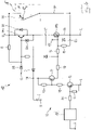
- FIG. 1 shows a schematic of a disconnecting device 1 which, in the exemplary embodiment, is connected between a direct voltage source 2 for generating a direct voltage U DC and a direct current I N and a load 3 .
- the separating device 1 comprises a circuit breaker arrangement in the form of a series connection of two magnetic, in particular hydraulic-magnetic, circuit breakers 5, 6, whose switching contacts coupled to a switching mechanism 7 are designated C 1 and C 2 .
- Another circuit breaker 8 or switching contact C 3 is in the reverse current or negative path (Return line) 9 of the separating device 1 is connected and also coupled to the switching mechanism 7 .
- Semiconductor electronics 10 are connected in parallel with one of the circuit breakers 5 , 6, 8, here the circuit breaker 5 or its switching contact C1.
- the circuit breakers 5, 6, 8 and the semiconductor electronics 10 form a self-sufficient hybrid circuit breaker as a separator 1 for nominal DC currents (direct currents) I N between 4A DC and 25oA DC at a direct voltage U DC between 300V DC and 1500V DC .
- the semiconductor electronics 10 essentially comprises at least one semiconductor switch 10a, 10b, which is connected in parallel to the protective switch 5 of the protective switch arrangement 5, 6, 8.
- the gate of an IGBT preferably used as a semiconductor switch 10b forms the control input or a control connection 11 of the semiconductor circuit 10. This control input or control connection 11 can be routed to the main current path 4 via a drive circuit.
- FIG 1 shows a four-pole disconnecting device 1 or a four-pole hybrid circuit breaker with supply-side inputs or input terminals E 1 and E 2 and load-side outputs or output terminals A 1 and A 2
- figure 2 a two-pole separator 1 or a two-pole hybrid circuit breaker is shown.
- the respective circuit breakers 5, 6, 8 or their switching contacts C 1 , C 2 , C 3 can each have a switching mechanism 7 and a magnetic or magnetic-hydraulic release 12 .
- the circuit breakers 5, 6, 8 are suitably assigned a common switching mechanism 7 and a common trigger (triggering device) 12.
- the switching contacts C n of the other circuit breakers are then preferably mechanically coupled to the switching mechanism 7 of the main circuit breaker, here the circuit breaker 5, in order to ensure at least approximately simultaneous tripping of the circuit breakers 5, 6, 8 and contact separation of the switching contacts C n of all circuit breakers 5, 6, 8 to effect the circuit breaker arrangement.
- the circuit breakers 5, 6, 8 or their switching contacts C n are assigned a drive 13 designed as a motor or magnet system. This is supplied with a control signal S A for circuit breaker tripping by a module 14, referred to below as the arc fault module, for arc detection or for detecting an overcurrent.
- the module 14 is connected to a current sensor 15 which detects the current I preferably flowing in the main current path 4 . The detected current I is evaluated by the module 14 .
- the Module 14 that Control or trigger signal S A generated.
- the circuit breakers 5, 6, 8 of the circuit breaker arrangement are triggered practically at the same time.
- An arc occurring in the course of the opening of their switching contacts C n causes a corresponding arcing voltage and a corresponding arcing current, which switches the previously current-blocking semiconductor electronics 10 conductive, so that the current flowing in the main current path 4 commutes to the semiconductor electronics 10 and is taken over by it until the arc is extinguished becomes.
- the semiconductor electronics 10 accepts switching currents up to a value of approximately 1000A within a very short period of time, the commutation being dependent on the circuit inductance within a corresponding time range of 50 ⁇ s to 300 ⁇ s. In the case of higher switching currents, the circuit breaker arrangement 5, 6, 8 alone takes over the shutdown and current limitation.
- a first semiconductor switch (IGBT) 10a can be seen connected in series in a cascode arrangement with a second semiconductor switch 10b in the form of a MOSFET.
- the cascode arrangement with the two semiconductor switches 10a, 10b thus forms analogously to 1 the commutation path 16 parallel to the protective switch 5 of the protective switch arrangement 5, 6, 8 and thus to the main current path 4.
- the first semiconductor switch 10a is routed between the direct current source 2 and the protective switch arrangement and there parallel to the switching contact C1 to the main current path 4.
- the potential U+ is always greater than the potential U ⁇ on the opposite side of the switch , on which the second semiconductor switch (MOSFET) 10b is connected to the main circuit 4 .
- the plus potential U+ is 0V when the switching contacts C n of the circuit breaker arrangement 5, 6, 8 are closed.
- the first semiconductor switch (IGBT) 10a is connected to a freewheeling diode D2.
- a first Zener diode D3 is connected to the potential U - on the anode side and to the gate (control input 11) of the first semiconductor switch (IGBT) 10a on the cathode side tied together.
- Another Zener diode D4 is connected to the control input 11 on the cathode side and to the emitter of the first semiconductor switch (IGBT) 10a on the anode side.
- a diode D1 is connected to a center or cascode tap 17 between the first and second semiconductor switches 10a and 10b of the cascode arrangement on the anode side, which is connected to the potential U ⁇ on the cathode side via a capacitor C serving as an energy store.
- a transistor T1 connected to ohmic resistors R1 and R2 is connected via further resistors R3 and R4 to the gate of the second semiconductor switch 10b, which in turn is connected to the control input 12 of the semiconductor electronics 10 tied together.
- Another Zener diode D5 with a parallel resistor R5 is connected to the gate on the cathode side and to the emitter of the second semiconductor switch 10b on the anode side.
- the transistor T1 On the base side, the transistor T1 is driven via a transistor T2, which in turn is connected on the base side via an ohmic resistor R6 to a timing element 19, which is designed as a monoflop, for example.
- the transistor T2 is also connected to a further resistor R7 on the base-emitter side.
- the commutation of the switch current I which essentially corresponds to the arc current, already begins from the main current path 4 to the commutation path 16 of the semiconductor electronics 10.
- the energy store C is charged during this arcing time interval.
- the duration is set such that on the one hand sufficient energy is available for reliable activation of the semiconductor electronics 10, in particular for switching it off during a specific period of time following the period of time representing the duration of the arc.
- the period is sufficiently short, so that an undesirable contact erosion or -wear of the switching contacts C n of the circuit breaker arrangement 5, 6, 8 is avoided.
- the first semiconductor switch 10a is controlled at least to the extent via the resistor R that a sufficient charging voltage and a sufficient arc or charging current for the capacitors C is available.
- U AB 12V (DC)
- the tap voltage is used to supply the control circuit of the electronics 10, which is essentially formed by the transistors T1 and T2 as well as the timer 19 and the energy store C.
- the diode D1 which is connected to the cascode tap 17 on the anode side and to the capacitor C on the cathode side, prevents the charging current from flowing back out of the Capacitors C and the commutation path 16 in the direction of the potential U - .
- the charging capacity and thus the storage energy contained in the capacitor C is dimensioned in such a way that the semiconductor electronics 10 carry the switch current I for a period of time specified by the timer 19 .
- This time period can be set to 3 ms, for example.
- the dimensioning of this period of time and thus the setting of the timer 19 are based essentially on the application-specific or typical periods of time for complete extinguishing of the arc and after sufficient cooling of the plasma formed in the process.
- the essential requirement here is that after the electronics 10 have been switched off, with the commutation path 16 then again having a high resistance and the semiconductor electronics 10 consequently blocking the current, no new arc can occur on the circuit breaker arrangement 5, 6, 8 which has still been triggered.
- the positive potential U+ thus goes towards this operating voltage when the commutation path 16 has a high resistance as a result of the blocking of the semiconductor switches 10 and the electronics 10 thus block the current again.
- an electrical device such. B. be provided an inverter of a photovoltaic system.
Landscapes
- Driving Mechanisms And Operating Circuits Of Arc-Extinguishing High-Tension Switches (AREA)
- Keying Circuit Devices (AREA)
- Emergency Protection Circuit Devices (AREA)
Description
- Die Erfindung betrifft eine Trennvorrichtung zur Gleichstromunterbrechung zwischen einer Gleichstromquelle und einer elektrischen Einreichung oder einer Last gemäß dem Oberbegriff des Anspruchs 1. Eine derartige Trennvorrichtung ist aus der
WO 2010/108565 A1 und aus deren prioritätsbegründendenDE 20 2009 004 198 U1 bekannt. Unter Gleichstrom (DC) wird hierbei ein Nennstrombereich zwischen 4ADC und 250ADC bei einem Gleichspannungsbereich zwischen 300VDC und 1500VDC verstanden. - Da eine derartige Gleichspannungsquelle, beispielsweise einer Photovoltaikanlage, systembedingt einerseits dauerhaft einen Betriebsstrom und eine Betriebsspannung im Bereich zwischen 180V (DC) und 1500V (DC) liefert und andererseits - beispielsweise zu Installations-, Montage- oder Servicezwecken sowie zum allgemeinen Personenschutz eine zuverlässige Trennung der elektrischen Komponenten, Einrichtungen und/oder einer Last von der Gleichstromquelle gewünscht ist, muss eine entsprechende Trennvorrichtung in der Lage sein, eine Unterbrechung unter Last, d.h. ohne vorheriges Abschalten der Gleichstromquelle vorzunehmen.
- Zur Lasttrennung kann ein mechanischer Schalter (Schaltkontakt) mit dem Vorteil eingesetzt werden, dass bei erfolgter Kontaktöffnung eine galvanische Trennung der elektrischen Einrichtung (Wechselrichter) von der Gleichstromquelle (Photovoltaikanlage) hergestellt ist. Nachteilig ist jedoch, dass derartige mechanische Schaltkontakte aufgrund des bei der Kontaktöffnung entstehenden Lichtbogens sehr schnell abgenutzt werden oder aber ein zusätzlicher Aufwand erforderlich ist, um den Lichtbogen einzuschließen und abzukühlen, was üblicherweise durch einen entsprechenden mechanischen Schalter mit einer Löschkammern erfolgt.
- Werden demgegenüber zur Lasttrennung leistungsfähige Halbleiterschalter eingesetzt, so treten auch im Normalbetrieb unvermeidbare Leistungsverluste an den Halbleitern auf. Zudem sind mit derartigen Leistungshalbleitern keine galvanische Trennung und damit kein zuverlässiger Personenschutz sichergestellt.
- Bei der aus der
WO 2010/108565 A1 (DE 20 2009 004 198 U1 ) bekannten Trennvorrichtung ist deren mechanischer Schalter im nicht ausgelösten Zustand der Trennvorrichtung stromführend. Dem mechanischen Schalter ist eine Halbleiterelektronik parallel geschaltet, die mit dem mechanischen Schalter derart verschaltet ist, dass bei sich öffnendem mechanischen Schalter zur Unterbrechung des Stromflusses durch die Trennvorrichtung aufgrund eines sich im Bereich des mechanischen Schalters ausbildenden Lichtbogens die Halbleiterelektronik stromleitend geschalten wird. - Hierfür weist die Halbleiterelektronik einen Energiespeicher auf, der infolge des Lichtbogens innerhalb der Dauer des Lichtbogens aufgeladen wird und mittels dessen die Halbleiterelektronik betrieben wird. Aufgrund der Stromleitfähigkeit der Halbleiterschaltung im Falle eines Lichtbogens ist diesem ein vergleichsweise niederohmiger Strompfad parallel geschalten, was zu einem vergleichsweise frühen Erlöschen des Lichtbogens und somit zu einer vergleichsweise geringen Belastung der Trennvorrichtung oder Unterbrechungseinheit führt.
- Aus der
DE 196 19 437 A1 ist ein Schaltgerät mit einem in einem Hauptstrompfad angeordneten Niederspannungsschalter bekannt, welcher in Reihe liegend mindestens ein den abzuschaltenden Strom abtastendes Auslöseelement und eine Hauptschaltstelle sowie einen parallel zur Hauptschaltstelle geschalteten Nebenstrompfad enthält. In diesem sind zueinander parallel geschaltet ein steuerbarer Halbleiterschalter und ein Entlastungselement angeordnet. Parallel zur Hauptschaltstelle liegt eine Steuervorrichtung des Halbleiterschalters. Der Nebenstrompfad enthält in Reihe geschaltet mit der Parallelschaltung aus steuerbarem Halbleiterschalter und Entlastungselement eine Hilfsschaltstelle, welche beim Ausschalten zeitverzögert nach dem Öffnen des Halbleiterschalters öffnet. - Der Erfindung liegt die Aufgabe zu Grunde, eine besonders geeignete Trennvorrichtung zur Gleichstromunterbrechung zwischen einer Gleichstromquelle und einer elektrischen Einrichtung oder Last anzugeben.
- Diese Aufgabe wird erfindungsgemäß gelöst durch die Merkmale des Anspruchs 1. Hierzu umfasst die nachfolgend auch als Hybridschutzschalter (hybrid circuit breaker) bezeichnete Trennvorrichtung eine mindestens einen ersten stromführenden Schutzschalter mit magnetischem Auslöser aufweisende Schutzschalteranordnung und eine dem ersten Schutzschalter der Schutzschalteranordnung parallel geschaltet Halbleiterelektronik, die im Wesentlichen zumindest einen Halbleiterschalter, vorzugsweise einen IGBT, umfasst. Unter Schutzschalter mit magnetischem Auslöser wird ein solcher mit rein magnetischer, mit thermisch-magnetischer oder mit hydraulisch-mechanischer Auslösung und somit allgemein ein magnetischer, thermisch-magnetischer oder hydraulisch-mechanischer Schutzschalter verstanden.
- Die Halbleiterelektronik ist dazu vorgesehen und eingerichtet, bei stromführendem Schutzschalter stromsperrend und bei einer Auslösung des Schutzschalters in Folge eines Überstroms und/oder eines Schaltsignals zumindest kurzeitig stromleitend zu sein, indem bei auslösendem Schutzschalter der Strom, d. h. ein infolge eines Lichtbogens erzeugter Lichtbogenstrom vom Schutzschalter auf die Halbleiterelektronik kommutiert.
- Die Halbleiterelektronik des erfindungsgemäßen Trennschalters weist vorzugsweise keinerlei zusätzliche Energiequelle auf und ist demzufolge bei geschlossenem mechanischem Schalter stromsperrend, d. h. hochohmig und somit praktisch strom- und spannungslos. Da über die Halbleiterelektronik bei geschlossenen mechanischen Schaltkontakten des oder jedes Schutzschalters der Schutzschalteranordnung kein Strom fließt und daher insbesondere über dem oder jedem Halbleiterschalter kein Spannungsfall erfolgt, erzeugt die Halbleiterschaltung bei geschlossenen Schaltkontakten der Schutzschalteranordnung auch keine Leistungsverluste. Vielmehr gewinnt die Halbleiterelektronik die zu deren Betrieb erforderliche Energie aus der Trennvorrichtung selbst. Dazu wird die Energie eines beim Öffnen der Schalterkontakte des oder jedes Schutzschalters der Schutzschalteranordnung entstehenden Lichtbogens genutzt. Hierbei ist geeigneterweise ein Steuereingang der Halbleiterelektronik bzw. des Halbleiterschalters derart mit dem oder jedem Schutzschalter verschaltet, dass bei sich öffnenden Schalterkontakten der Schutzschalteranordnung die Lichtbogenspannung die hierzu parallele Halbleiterelektronik stromleitend, d. h. niederohmig und somit stromführend schaltet.
- Sobald die Halbleiterelektronik bereits geringfügig stromleitend geschaltet ist, beginnt der Lichtbogenstrom vom Schutzschalter bzw. von dessen Schaltkontakten auf die Halbleiterelektronik zu kommutieren. Indem die Schutzschalteranordnung der Trennvorrichtung mindestens einen zweiten Schutzschalter aufweist, die bzw. deren Schaltkontakten in Reihe geschaltet sind, und der mindestens eine erste Schutzschalter der Schutzschalteranordnung mit der Halbleiterelektronik in Reihe geschaltet ist, wird im Auslösefall der Schutzschalteranordnung eine galvanische Trennung der Last von der Gleichstromquelle und somit durch Öffnen dieses Hybridschutzschalters eine vollständige galvanische Gleichstromunterbrechung erzielt.
- Gemäß einer besonders vorteilhaften Weiterbildung der Trennvorrichtung weist diese ein Modul (Arc Fault Module) zur Lichtbogenerfassung und/oder zur Lichtbogenerkennung auf. Dieses Modul wirkt mit einem Stromsensor zur Erfassung des über den oder jeden Schutzschalter fließenden Stroms zusammen, ist mit dem Stromsensor also elektrisch verbunden. Das Modul wertet den erfassten Strom hinsichtlich dessen zeitlichen Verlauf und/oder dessen Steilheit (dl/dt) aus. Wird ein bestimmtes Charakteristikum des erfassten Stromes erkannt, wenn also beispielsweise auf einen Lichtbogen geschlossen wird, so übermittelt das Modul eine Auslösesignal an den oder jeden Schutzschalter zu dessen Auslösung. Hierzu ist das Modul vorzugsweise mit einem motorischen oder magnetischen Antrieb verbunden, der seinerseits mit dem oder jedem Schutzschalter bzw. mit dessen/deren Schaltschloss zur Trennung der Schutzschalterkontakte gekoppelt ist.
- Die Trennvorrichtung kann zweipolig oder vierpolige ausgeführt sein. Bei vierpoliger Trennvorrichtung ist mindestens ein Schutzschalter der Schutzschalteranordnung, vorzugsweise eine Reihenschaltung aus mindestens zwei Schutzschaltern mit Schutzschaltertrennkontakten, in einen Hauptstrompfad (Plusstrompfad) der Trennvorrichtung geschaltet. Zusätzlich oder alternativ ist mindestens ein Schutzschalter bzw. Schutzschaltertrennkontakt der Schutzschalteranordnung in den Rückstrompfad (Minusstrompfad) der Trennvorrichtung geschalteten.
- Nachfolgend werden Ausführungsbeispiele der Erfindung anhand einer Zeichnung näher erläutert. Darin zeigen:
- Fig. 1
- in einem Blockschaltbild eine vierpolige Variante der Trennvorrichtung mit einer Schautzschalteranordnung mit einer Reihenschaltung aus drei magnetischen/magnetisch-hydraulischen Schutzschaltern und einer zu einem der Schutzschalter bzw. zu dessen Schaltkontakten parallelen Halbleiterelektronik,
- Fig. 2
- in einem Blockschaltbild gemäß
Figur 1 eine zweipolige Variante der Trennvorrichtung, - Fig. 3
- in einem Blockschaltbild die zweipolige Trennvorrichtung mit einem Arc Fault Modul und mit einem Antrieb zur Auslösung der Schutzschalteranordnung, und
- Fig. 4
- das Schaltbild einer an sich bekannten Halbleiterelektronik der Trennvorrichtung.
- Einander entsprechende Teile sind in beiden Figuren mit den gleichen Bezugszeichen versehen.
-
Fig. 1 zeigt schematisch eine Trennvorrichtung 1, die im Ausführungsbeispiel zwischen eine Gleichspannungsquelle 2 zur Erzeugung einer Gleichspannung UDC und eines Gleichstroms IN sowie eine Last 3 geschaltet ist. Die Trennvorrichtung 1 umfasst im den Pluspol repräsentierenden Hauptstrom- oder Pluspfad 4 eine Schutzschalteranordnung in Form einer Reihenschaltung aus zwei magnetischen, insbesondere hydraulisch-magnetischen, Schutzschaltern 5, 6, deren mit einem Schaltschloss 7 gekoppelten Schaltkontakte mit C1 und C2 bezeichnet sind. Ein weiterer Schutzschalter 8 bzw. Schaltkontakt C3 ist in den Rückstrom- oder Minuspfad (Rückführleitung) 9 der Trennvorrichtung 1 geschaltet und ebenfalls mit dem Schaltschloss 7 gekoppelt. - Einem der Schutzschalter 5, 6, 8, hier dem Schutzschalter 5 bzw. dessen Schaltkontakt C1 ist eine Halbleiterelektronik 10 parallel geschaltet. Die Schutzschalter 5, 6, 8 und die Halbleiterelektronik 10 bilden einen autarken Hybridschutzschalter als Trennvorrichtung 1 für DC-Nennströme (Gleichströme) IN zwischen 4ADC und 25oADC bei einer Gleichspannung UDC zwischen 300VDC und 1500VDC. Die Halbleiterelektronik 10 umfasst im Wesentlichen mindestens einen Halbleiterschalter 10a, 10b, der dem Schutzschalter 5 der Schutzschalteranordnung 5, 6, 8 parallel geschaltet ist. Das Gate eines vorzugsweise als Halbleiterschalter 10b eingesetzten IGBT's bildet den Steuereingang bzw. einen Steueranschluss 11 der Halbleiterschaltung 10. Dieser Steuereingang oder Steueranschluss 11 kann über eine Ansteuerschaltung an den Hauptstrompfad 4 geführt sein.
- Während
Figur 1 eine vierpolige Trennvorrichtung 1 beziehungsweise einen vierpoligen Hybridschutzschalter mit versorgungsseitigen Eingängen oder Eingangsanschlüssen E1 und E2 sowie lastseitigen Ausgängen beziehungsweise Ausgangsanschlüssen A1 und A2 zeigt, ist inFigur 2 eine zweipolige Trennvorrichtung 1 beziehungsweise ein zweipoliger Hybridschutzschalter dargestellt. Die jeweiligen Schutzschalter 5, 6, 8 beziehungsweise deren Schaltkontakte C1, C2, C3 können jeweils ein Schaltschloss 7 und einen magnetischen beziehungsweise magnetisch-hydraulischen Auslöser 12 aufweisen. Geeigneterweise ist jedoch - wie dargestellt - den Schutzschaltern 5, 6, 8 ein gemeinsames Schaltschloss 7 und ein gemeinsamer Auslöser (Auslösevorrichtung) 12 zugeordnet. Die Schaltkontakte Cn der weiteren Schutzschalter sind dann mit dem Schaltschloss 7 des Hauptschutzschalters, hier des Schutzschalters 5 vorzugsweise mechanisch gekoppelt, um eine zumindest annähernd zeitgleiche Auslösung der Schutzschalter 5, 6, 8 und Kontakttrennung der Schaltkontakte Cn aller Schutzschalter 5, 6, 8 der Schutzschalteranordnung zu bewirken. - Die in
Figur 3 gezeigte Ausführungsform der Trennvorrichtung 1 beziehungsweise des Hybridschutzschalters ist wiederum zweipolig, wobei analog auch diese Ausführungsform als vierpolige Trennvorrichtung 1 ausgeführt sein kann. - Bei dieser Ausführungsform ist den Schutzschaltern 5, 6, 8 beziehungsweise deren Schaltkontakten Cn ein als Motor oder Magnetsystem ausgeführter Antrieb 13 zugeordnet. Diesem wird von einem nachfolgend als Arc Fault Module bezeichneten Modul 14 zur Lichtbogendetektion oder zur Erkennung eines Überstroms ein Steuersignal SA zur Schutzschalterauslösung zugeführt. Das Modul 14 ist mit einem Stromsensor 15 verbunden, welcher den vorzugsweise im Hauptstrompfad 4 fließenden Strom I erfasst. Der erfasste Strom I wird mittels des Moduls 14 ausgewertet.
- Bei Erfüllung bestimmter Kriterien, beispielsweise bei einer Überschreitung einer Stromgrenze mit 105% bis 150% des Nennstroms (1,05 · IN bis 1,5 · IN) und/oder im Falle einer gewissen Stromsteilheit (dl/dt) wird vermittels des Moduls 14 das Steuer- oder Auslösesignal SA erzeugt. In Folge dessen werden die Schutzschalter 5, 6, 8 der Schutzschalteranordnung praktisch zeitgleich ausgelöst. Ein im Zuge des Öffnens deren Schaltkontakte Cn entstehender Lichtbogen bewirkt eine entsprechende Lichtbogenspannung und einen entsprechenden Lichtbogenstrom, der die zuvor stromsperrende Halbleiterelektronik 10 stromleitend schaltet, sodass der im Hauptstrompfad 4 fließende Strom auf die Halbleiterelektronik 10 kommutiert und von dieser bis zum Erlöschen des Lichtbogens übernommen wird.
- Die Halbleiterelektronik 10 übernimmt Schaltströme bis zu einem Wert von ca. 1000A innerhalb einer sehr kurzen Zeitspanne, wobei die Kommutierung innerhalb eines entsprechenden Zeitbereiches von 50µs bis 300µs abhängig von der Kreisinduktivität ist. Bei höheren Schaltströmen übernimmt die der Schutzschalteranordnung 5, 6, 8 allein die Abschaltung und eine Strombegrenzung.
-
Fig. 4 zeigt die Schaltung einer möglichen, bevorzugt eingesetzten Halbleiterelektronik 10, die dem Schutzschalter 5 der Schutzschalteranordnung 5, 6, 8 des autarken Hybridschutzschalters als Trennvorrichtung 1 parallel geschaltet ist. Erkennbar ist ein erster Halbleiterschalter (IGBT) 10a in einer Kaskodenanordnung mit einem zweiten Halbleiterschalter 10b in Form eines MOSFET in Reihe geschaltet. Die Kaskodenanordnung mit den beiden Halbleiterschaltern 10a, 10b bildet somit analog zurFig. 1 den zum Schutzschalter 5 der Schutzschalteranordnung 5, 6, 8 und somit zum Hauptstrompfad 4 parallelen Kommutierungspfad 16. Der erste Halbleiterschalter 10a ist zwischen der Gleichstromquelle 2 und der Schutzschalteranordnung und dort parallel zum Schaltkontakt C1 an den Hauptstrompfad 4 geführt. Dort ist das Potential U+ stets größer als das Potential U- auf der gegenüberliegenden Schalterseite, an der der zweite Halbleiterschalter (MOSFET) 10b an den Hauptstromkreis 4 geführt ist. Das Pluspotential U+ beträgt 0V, wenn die Schaltkontakte Cn der Schutzschalteranordnung 5, 6, 8 geschlossen sind. - Der erste Halbleiterschalter (IGBT) 10a ist mit einer Freilaufdiode D2 beschaltet. Eine erste Zehnerdiode D3 ist anodenseitig gegen das Potential U- und kathodenseitig mit dem Gate (Steuereingang 11) des ersten Halbleiterschalters (IGBT) 10a verbunden. Eine weitere Zehnerdiode D4 ist kathodenseitig wiederum mit dem Steuereingang 11 und anodenseitig mit dem Emitter des ersten Halbleiterschalters (IGBT) 10a verbunden. An einen Mitten- oder Kaskodenabgriff 17 zwischen dem ersten und zweiten Halbleiterschalter 10a bzw. 10b der Kaskodenanordnung ist anodenseitig eine Diode D1 geführt, die kathodenseitig über einen als Energiespeicher dienenden Kondensator C gegen das Potential U- geschaltet ist. Über einen anodenseitigen Spannungsabgriff 18 zwischen der Diode D1 und dem Energiespeicher bzw. dem Kondensator C ist ein mit ohmschen Widerständen R1 und R2 beschalteter Transistor T1 über weitere Widerstände R3 und R4 mit dem wiederum an den Steuereingang 12 der Halbleiterelektronik 10 geführten Gate des zweiten Halbleiterschalters 10b verbunden. Eine weitere Zehnerdiode D5 mit parallelem Widerstand R5 ist kathodenseitig mit dem Gate und anodenseitig mit dem Emitter des zweiten Halbleiterschalters 10b verbunden.
- Basisseitig wird der Transistor T1 über einen Transistor T2 angesteuert, der seinerseits basisseitig über einen ohmschen Widerstand R6 mit einem beispielsweise als Monoflopp ausgeführten Zeitglied 19 verbunden ist. Basis-emitter-seitig ist der Transistor T2 zudem mit einem weiteren Widerstand R7 beschaltet.
- Während der dem Öffnungszeitpunkt der Schalterkontakte Cn der Schutzschalteranordnung 5, 6, 8 nachfolgenden Zeitdauer (Lichtbogenzeitintervall) beginnt bereits die Kommutierung des im Wesentlichen dem Lichtbogenstrom entsprechenden Schalterstroms I vom Hauptstrompfad 4 auf den Kommutierungspfad 16 der Halbleiterelektronik 10. Während der Lichtbogen-Zeitdauer teilt sich praktisch der Lichtbogenstrom zwischen dem Hauptstrompfad 4, also über die Schutzschalter 5, 6, 8 und den Kommutierungspfad 16, also die Halbleiterelektronik 10 auf. Während dieses Lichtbogenzeitintervalls wird der Energiespeicher C geladen. Die Zeitdauer ist dabei derart eingestellt, dass einerseits genügend Energie für ein zuverlässiges Ansteuern der Halbleiterelektronik 10 zur Verfügung steht, insbesondere zu deren Abschaltung während eines bestimmten Zeitraums im Anschluss an die die Lichtbogendauer repräsentierende Zeitdauer. Andererseits ist die Zeitdauer ausreichend kurz, so dass ein unerwünschter Kontaktabbrand oder -verschleiß der Schaltkontakte Cn der Schutzschalteranordnung 5, 6, 8 vermieden ist.
- Mit Beginn des Lichtbogens und somit bei Entstehung der Lichtbogenspannung wird über den Widerstand R der erste Halbleiterschalter 10a zumindest soweit durchgesteuert, dass eine ausreichende Ladespannung und ein ausreichender Lichtbogen- bzw. Ladestrom für die Kondensatoren C zur Verfügung steht. Hierzu wird mit der entsprechenden Beschaltung des ersten Halbleiterschalters 10a mit dem Widerstand R und der Zehnerdiode D3 ein Regelkreis der Elektronik 10 geschaffen, mit dem die Spannung am Kaskodenabgriff 17 auf beispielsweise UAB = 12V (DC) eingestellt ist. Hierbei fließt durch den dem Pluspotential U+ nahen ersten Halbleiterschalter 10a ein Bruchteil des Lichtbogenstroms und damit des Schaltstroms I der hybriden Trennvorrichtung 1.
- Die Abgriffsspannung dient zur Versorgung der im Wesentlichen durch die Transistoren T1 und T2 sowie das Zeitglied 19 und den Energiespeicher C gebildeten Ansteuerschaltung der Elektronik 10. Die anodenseitig mit dem Kaskodenabgriff 17 und kathodenseitig mit dem Kondensator C verbundene Diode D1 verhindert einen Rückfluss des Ladestroms aus den Kondensatoren C und über den Kommutierungspfad 16 in Richtung des Potentials U-.
- Ist genügend Energie im Kondensator C und somit im Energiespeicher enthalten, und ist demzufolge eine ausreichend hohe Steuer- oder Schaltspannung am Spannungsabgriff 18 vorhanden, so steuern der Transistor T1 und in Folge dessen der Transistor T2 durch, so dass auch die beiden Halbleiterschalter 10a, 10b vollständig durchsteuern. Der Lichtbogen- bzw. Schalterstrom I fließt aufgrund des im Vergleich zum sehr hohen Widerstand der von der geöffneten Schutzschalteranordnung 5, 6, 8 gebildeten Trennstrecke des Hauptstrompfades 4 wesentlich geringeren Widerstandes der nunmehr durchgesteuerten Halbleiterschalter 10a, 10b praktisch ausschließlich über den Kommutierungspfad 16. Das Pluspotential U+ geht somit erneut gegen 0V, wenn der Schaltstrom I auf die Elektronik 10 kommutiert. In Folge dessen verlöscht der Lichtbogen zwischen den Kontakten Cn der Schutzschalteranordnung 5, 6, 8.
- Die Ladekapazität und somit die in dem Kondensator C enthaltene Speicherenergie ist derart bemessen, dass die Halbleiterelektronik 10 den Schalterstrom I für eine vom Zeitglied 19 vorgegebene Zeitdauer trägt. Diese Zeitdauer kann auf beispielsweise 3ms eingestellt sein. Die Bemessung dieser Zeitdauer und damit die Festlegung des Zeitgliedes 19 richten sich im Wesentlichen nach den anwendungsspezifischen oder typischen Zeitdauern für ein vollständiges Verlöschen des Lichtbogens sowie nach einer ausreichenden Abkühlung des dabei gebildeten Plasmas. Wesentliche Maßgabe ist hierbei, dass nach erfolgter Abschaltung der Elektronik 10 mit daraufhin wiederum hochohmigem Kommutierungspfad 16 und demzufolge stromsperrender Halbleiterelektronik 10 an der nach wie vor ausgelösten Schutzschalteranordnung 5, 6, 8 kein erneuter Lichtbogen entstehen kann.
- Nach Ablauf der durch das Zeitglied 19 festgelegten Zeitdauer sinkt der Schaltstrom I auf praktisch Null (I = 0A) ab, während zeitgleich die Schalterspannung auf die von der Gleichstromquelle UDC gelieferte Betriebsspannung mit beispielsweise ansteigt. Das Pluspotential U+ geht somit gegen diese Betriebsspannung, wenn der Kommutierungspfad 16 infolge der Sperrung der Halbleiterschalter 10 hochohmig und somit die Elektronik 10 erneut stromsperrend wird.
- Da zu diesem Zeitpunkt der Hauptstrompfad 4 bei gleichzeitig hochohmigem Kommutierungspfad 16 galvanisch geöffnet ist, ist bereits eine lichtbogenfreie Gleichstromunterbrechung zwischen der Gleichstromquelle UDC und der Last 3 hergestellt. Demzufolge ist die Verbindung zwischen der Gleichstromquelle und der Last 3 bereits zuverlässige getrennt. Als oder anstelle der Last 3 kann auch eine elektrische Einrichtung, z. B. ein Wechselrichter einer Photovoltaikanlage vorgesehen sein.
-
- 1
- Trennvorrichtung/Hybridschutzschalter
- 2
- Gleichstromquelle
- 3
- Last/Einrichtung
- 4
- Hauptstrom-/Pluspfad
- 5
- Schutzschalter
- 6
- Schutzschalter
- 7
- Schaltschloss
- 8
- Schutzschalter
- 9
- Rückstrom-/Minuspfad
- 10
- Halbleiterelektronik
- 10a
- erster Halbleiterschalter
- 10b
- zweiter Halbleiterschalter
- 11
- Steuereingang
- 12
- Auslöser/Auslösevorrichtung
- 13
- Antrieb
- 14
- Arc Fault Modul
- 15
- Stromsensor
- 16
- Kommutierungspfad
- 17
- Kaskoden-/Mittenabgriff
- 18
- Spannungsabgriff
- 19
- Zeitglied
- A1,2
- Ausgang/Ausgangsanschluss
- Cn
- Schaltkontakt
- E1,2
- Eingang/Eingangsanschluss
- I
- Strom
- IN
- Nennstrom
- SA
- Steuer-/Auslösesignal
- UDC
- Gleichspannung
Claims (6)
- Trennvorrichtung (1) zur Gleichstromunterbrechung zwischen einer Gleichstromquelle (UDC) und einer Last (3), aufweisend- eine Schutzschalteranordnung mit einem ersten Schutzschalter (5) und mit mindestens einem zweiten Schutzschalter (6, 8), der mit dem ersten Schutzschalter (5) in Reihe geschaltet ist, und- eine dem ersten Schutzschalter (5) parallel geschaltete Halbleiterelektronik (10), die bei stromführender Schutzschalteranordnung stromsperrend und bei auslösender Schutzschalteranordnung zumindest kurzzeitig stromleitend ist, indem bei auslösender Schutzschalteranordnung ein infolge eines Lichtbogens erzeugter Lichtbogenstrom vom ersten Schutzschalter (5) auf die Halbleiterelektronik (10) kommutiert,- wobei zum Zwecke einer galvanischen Trennung der Last (3) von der Gleichstromquelle (UDC) im Auslösefall der zweite Schutzschalter (6, 8) der Schutzschalteranordnung mit der Halbleiterelektronik (10) in Reihe geschaltet ist,
dadurch gekennzeichnet,- dass zumindest der erste Schutzschalter (5) einen magnetischen Auslöser (12) aufweist,- dass der erste Schutzschalter (5) und der oder jeder zweite Schutzschalter (6, 8) bzw. deren Schaltkontakte (C1, C2, C3) mittels eines Schaltschlosses (7) gekoppelt sind, und- dass mit dem oder jedem Schutzschalter (5, 6, 8) der Schutzschalteranordnung ein Antrieb (13) zur Auslösung jedes Schutzschalters (5, 6, 8) im Falle eines, insbesondere bei Auftreten des Lichtbogens, erfassten Überstroms gekoppelt ist. - Trennvorrichtung (1) nach Anspruch 1,
dadurch gekennzeichnet,
dass die Halbleiterelektronik (10) mindestens einen steuerbaren Halbleiterschalter (10a, 10b) aufweist. - Trennvorrichtung (1) nach Anspruch 1 oder 2,
dadurch gekennzeichnet,
dass ein Steuereingang (11) der Halbleiterelektronik (10) derart mit dem ersten Schutzschalter (5) der Schutzschalteranordnung verschaltet ist, dass bei sich öffnendem Schutzschalter (5) oder Schaltkontakt (C1) eine infolge eines Lichtbogens über dem Schutzschalter (5) bzw. über dessen Schaltkontakt (C1) erzeugte Lichtbogenspannung die Halbleiterelektronik (10) stromleitend schaltet. - Trennvorrichtung (1) nach einem der Ansprüche 1 bis 3,
dadurch gekennzeichnet,
dass ein mit einem Stromsensor (15) zur Erfassung des über den oder jeden Schutzschalter (5, 6, 8) der Schutzschalteranordnung fließenden Stroms (I) zusammenwirkendes Modul (14) zur Lichtbogenerfassung und/oder Lichtbogenerkennung oder zur Erkennung eines Überstroms vorgesehen ist. - Vierpolige Trennvorrichtung (1) nach einem der Ansprüche 1 bis 4, aufweisend- einen ersten Eingangsanschluss (E1) und einen ersten Ausgangsanschluss (A1),- einen zweiten Eingangsanschluss (E2) und einen zweiten Ausgangsanschluss (A2),- einen Hauptstrompfad (4) zwischen dem ersten Eingangsanschluss (E1) und dem ersten Ausgangsanschluss (A1), wobei die Schutzschalteranordnung mit dem ersten Schutzschalter (5) mit ersten Schaltkontakten(C1) und mit dem zweiten Schutzschalter (6) mit zweiten Schaltkontakten (C2) in den Hauptstrompfad (4) geschaltet ist, und- einen Rückstrompfad (9) zwischen dem zweiten Eingangsanschluss (E2) und dem zweiten Ausgangsanschluss (A2), wobei in den Rückstrompfad (9) ein dritter Schutzschalter (8) mit dritten Schaltkontakten (C3) geschaltet ist.
- Trennvorrichtung (1) nach Anspruch 5,
dadurch gekennzeichnet,
dass die Schaltkontakt (C1, C2, C3) der Schutzschalteranordnung (5, 6, 8) mittels eines gemeinsamen Schaltschlosses (7) gekoppelt sind.
Priority Applications (1)
| Application Number | Priority Date | Filing Date | Title |
|---|---|---|---|
| EP20207521.4A EP3855465B1 (de) | 2014-06-18 | 2015-03-16 | Trennschalter zur gleichstromunterbrechung |
Applications Claiming Priority (2)
| Application Number | Priority Date | Filing Date | Title |
|---|---|---|---|
| DE102014008706.9A DE102014008706A1 (de) | 2014-06-18 | 2014-06-18 | Trennschalter zur Gleichstromunterbrechung |
| PCT/EP2015/000576 WO2015192924A1 (de) | 2014-06-18 | 2015-03-16 | Trennschalter zur gleichstromunterbrechung |
Related Child Applications (2)
| Application Number | Title | Priority Date | Filing Date |
|---|---|---|---|
| EP20207521.4A Division EP3855465B1 (de) | 2014-06-18 | 2015-03-16 | Trennschalter zur gleichstromunterbrechung |
| EP20207521.4A Division-Into EP3855465B1 (de) | 2014-06-18 | 2015-03-16 | Trennschalter zur gleichstromunterbrechung |
Publications (2)
| Publication Number | Publication Date |
|---|---|
| EP3158571A1 EP3158571A1 (de) | 2017-04-26 |
| EP3158571B1 true EP3158571B1 (de) | 2022-08-03 |
Family
ID=52814044
Family Applications (2)
| Application Number | Title | Priority Date | Filing Date |
|---|---|---|---|
| EP15714411.4A Active EP3158571B1 (de) | 2014-06-18 | 2015-03-16 | Trennschalter zur gleichstromunterbrechung |
| EP20207521.4A Active EP3855465B1 (de) | 2014-06-18 | 2015-03-16 | Trennschalter zur gleichstromunterbrechung |
Family Applications After (1)
| Application Number | Title | Priority Date | Filing Date |
|---|---|---|---|
| EP20207521.4A Active EP3855465B1 (de) | 2014-06-18 | 2015-03-16 | Trennschalter zur gleichstromunterbrechung |
Country Status (6)
| Country | Link |
|---|---|
| US (1) | US10931093B2 (de) |
| EP (2) | EP3158571B1 (de) |
| JP (1) | JP2017527067A (de) |
| CN (1) | CN106663557B (de) |
| DE (1) | DE102014008706A1 (de) |
| WO (1) | WO2015192924A1 (de) |
Families Citing this family (21)
| Publication number | Priority date | Publication date | Assignee | Title |
|---|---|---|---|---|
| DE202015009288U1 (de) | 2015-10-08 | 2017-01-23 | Ellenberger & Poensgen Gmbh | Elektronischer Schutzschalter |
| EP3417468B1 (de) * | 2016-03-11 | 2020-11-18 | Siemens Aktiengesellschaft | Schaltanlagenanordnung, umrichteranordnung mit schaltanlagenanordnung und verfahren zum schutz der umrichteranordnung |
| DE102016105544A1 (de) * | 2016-03-24 | 2017-09-28 | Epcos Ag | Vorrichtung zur Messung eines Zustands eines elektrischen Schalters, elektrischer Schalter und Verfahren zur Messung eines Zustands eines elektrischen Schalters |
| DE102017101452A1 (de) | 2017-01-25 | 2018-07-26 | Eaton Industries (Austria) Gmbh | Niederspannungs-Schutzschaltgerät |
| WO2018198538A1 (ja) * | 2017-04-26 | 2018-11-01 | ソニー株式会社 | アーク抑制装置、移動体及び電力供給システム |
| US10629391B2 (en) | 2017-12-21 | 2020-04-21 | Eaton Intelligent Power Limited | Fusible safety disconnect in solid state circuit breakers and combination motor starters |
| CN112292744B (zh) * | 2018-06-27 | 2024-03-19 | 打矢恒温器株式会社 | 电子设备 |
| EP3594979A1 (de) * | 2018-07-09 | 2020-01-15 | ABB Schweiz AG | Vorrichtung zur umschaltung einer led |
| JP6694177B2 (ja) * | 2018-10-30 | 2020-05-13 | 嶋田 隆一 | 直流遮断装置 |
| US11615925B2 (en) | 2018-12-26 | 2023-03-28 | Eaton Intelligent Power Limited | Hazardous location compliant circuit protection devices having enhanced safety intelligence, systems and methods |
| US11270854B2 (en) | 2018-12-26 | 2022-03-08 | Eaton Intelligent Power Limited | Circuit protection devices, systems and methods for explosive environment compliance |
| EP3694105A1 (de) | 2019-02-05 | 2020-08-12 | Siemens Aktiengesellschaft | Schaltvorrichtung zum auftrennen eines strompfads |
| US12176163B2 (en) | 2019-03-29 | 2024-12-24 | Siemens Aktiengesellschaft | Electric grid and method for operating an electric grid |
| EP3739707A1 (de) | 2019-05-17 | 2020-11-18 | Siemens Aktiengesellschaft | Überstromschutzvorrichtung für den schutz eines in einem gleichstromnetz angeordneten verbrauchers |
| EP3999920B1 (de) * | 2019-09-17 | 2024-08-28 | Ellenberger & Poensgen GmbH | System mit einer steuerung und mit einem aktor sowie mit einer baugruppe zur bereitstellung von funktionaler sicherheit |
| US11482851B2 (en) * | 2020-10-14 | 2022-10-25 | Eaton Intelligent Power Limited | Arc flash mitigation device |
| ES2956365T3 (es) * | 2020-12-15 | 2023-12-20 | Abb Schweiz Ag | Un aparato de conmutación híbrido para redes eléctricas |
| DE102021113589A1 (de) * | 2021-05-26 | 2022-12-01 | Lisa Dräxlmaier GmbH | Elektronischer stromverteiler |
| KR102932071B1 (ko) * | 2021-09-30 | 2026-02-26 | 파나소닉 아이피 매니지먼트 가부시키가이샤 | 차단 장치 및 구동 장치 |
| DE102022134287B3 (de) * | 2022-12-21 | 2024-01-18 | Semikron Elektronik Gmbh & Co. Kg | Ansteuereinrichtung, Halbbrückenschaltungsanordnung damit und Verfahren dazu |
| US12444919B1 (en) * | 2023-03-28 | 2025-10-14 | Amazon Technologies, Inc. | System for operation of enhanced circuit breakers |
Family Cites Families (24)
| Publication number | Priority date | Publication date | Assignee | Title |
|---|---|---|---|---|
| JPS6178020A (ja) * | 1984-09-26 | 1986-04-21 | 三菱電機株式会社 | 電力開閉装置 |
| US4598330A (en) * | 1984-10-31 | 1986-07-01 | International Business Machines Corporation | High power direct current switching circuit |
| EP0231469B1 (de) * | 1986-01-31 | 1991-07-03 | BBC Brown Boveri AG | Leistungsschalter |
| FR2606929B1 (fr) * | 1986-11-14 | 1989-02-10 | Telemecanique Electrique | Dispositif interrupteur pour appareil de protection |
| US5410442A (en) * | 1992-02-17 | 1995-04-25 | Siemens Aktiengesellschaft | Electromechanical protection devcie |
| US5519561A (en) * | 1994-11-08 | 1996-05-21 | Eaton Corporation | Circuit breaker using bimetal of thermal-magnetic trip to sense current |
| JPH08315666A (ja) * | 1995-05-12 | 1996-11-29 | Mitsubishi Electric Corp | 遮断器および遮断装置 |
| DE19619437C2 (de) * | 1996-05-14 | 2003-01-16 | Abb Schweiz Ag | Schaltgerät |
| FR2794890B1 (fr) * | 1999-06-08 | 2001-08-10 | Crouzet Automatismes | Relais electromecanique assiste a la commutation par semi-conducteur |
| KR100434153B1 (ko) | 2002-04-12 | 2004-06-04 | 엘지산전 주식회사 | 하이브리드 직류 전자 접촉기 |
| JP2006032121A (ja) * | 2004-07-16 | 2006-02-02 | Japan Ae Power Systems Corp | 高電圧大容量遮断器 |
| DE102005006953A1 (de) * | 2005-02-16 | 2006-08-17 | Abb Patent Gmbh | Schaltgerät mit PTC-Element |
| US8879218B2 (en) * | 2007-12-14 | 2014-11-04 | True-Safe Technologies, Inc. | Arc fault circuit interrupter, systems, apparatus and methods of detecting and interrupting electrical faults |
| JP2009206066A (ja) * | 2008-02-27 | 2009-09-10 | Daito Communication Apparatus Co Ltd | ハイブリッド型直流リレー |
| CN101752148B (zh) * | 2008-12-12 | 2014-08-13 | 施耐德电器工业公司 | 带选择性的断路器 |
| DE202009004198U1 (de) * | 2009-03-25 | 2010-08-12 | Ellenberger & Poensgen Gmbh | Trennschalter zur galvanischen Gleichstromunterbrechung |
| FR2952470A1 (fr) * | 2009-11-06 | 2011-05-13 | Schneider Electric Ind Sas | Disjoncteur limiteur de courant, dispositif de distribution electrique pourvu d'un tel disjoncteur limiteur et procede de limitation de courant |
| DE102009059839A1 (de) * | 2009-12-21 | 2011-06-22 | Eaton Industries GmbH, 53115 | Vorrichtung zum Erkennen der Stromrichtungsumkehr |
| JP5291660B2 (ja) * | 2010-04-13 | 2013-09-18 | 日本電信電話株式会社 | 遮断装置 |
| JP5669537B2 (ja) * | 2010-11-30 | 2015-02-12 | 富士電機株式会社 | 電力監視制御装置およびブレーカ |
| JP5793019B2 (ja) * | 2011-08-19 | 2015-10-14 | 富士電機株式会社 | 消弧装置および開閉器 |
| DE102011056577C5 (de) * | 2011-12-19 | 2015-02-19 | Sma Solar Technology Ag | Schaltungsanordnung zur Unterdrückung eines bei einem Schaltvorgang auftretenden Lichtbogens |
| DE202012007257U1 (de) * | 2012-07-26 | 2013-10-28 | Ellenberger & Poensgen Gmbh | Vorrichtung zum sicheren Schalten einer Photovoltaikanlage |
| DE102013114259A1 (de) * | 2013-12-17 | 2015-06-18 | Eaton Electrical Ip Gmbh & Co. Kg | Schaltvorrichtung zum Führen und Trennen von elektrischen Strömen |
-
2014
- 2014-06-18 DE DE102014008706.9A patent/DE102014008706A1/de not_active Ceased
-
2015
- 2015-03-16 EP EP15714411.4A patent/EP3158571B1/de active Active
- 2015-03-16 CN CN201580032448.4A patent/CN106663557B/zh active Active
- 2015-03-16 EP EP20207521.4A patent/EP3855465B1/de active Active
- 2015-03-16 JP JP2016569977A patent/JP2017527067A/ja active Pending
- 2015-03-16 WO PCT/EP2015/000576 patent/WO2015192924A1/de not_active Ceased
-
2016
- 2016-12-19 US US15/383,416 patent/US10931093B2/en active Active
Also Published As
| Publication number | Publication date |
|---|---|
| CN106663557A (zh) | 2017-05-10 |
| DE102014008706A1 (de) | 2015-12-24 |
| EP3855465C0 (de) | 2023-10-11 |
| US20170098931A1 (en) | 2017-04-06 |
| EP3158571A1 (de) | 2017-04-26 |
| EP3855465B1 (de) | 2023-10-11 |
| EP3855465A1 (de) | 2021-07-28 |
| US10931093B2 (en) | 2021-02-23 |
| CN106663557B (zh) | 2019-05-10 |
| JP2017527067A (ja) | 2017-09-14 |
| WO2015192924A1 (de) | 2015-12-23 |
Similar Documents
| Publication | Publication Date | Title |
|---|---|---|
| EP3855465B1 (de) | Trennschalter zur gleichstromunterbrechung | |
| EP2411990B1 (de) | Trennschalter zur galvanischen gleichstromunterbrechung | |
| EP3320553B1 (de) | Trennvorrichtung zur gleichstromunterbrechung | |
| DE3735009A1 (de) | Leistungstrennschalter | |
| EP3542386B1 (de) | Niederspannungs-schutzschaltgerät | |
| DE3717491A1 (de) | Elektronischer leistungstrennschalter | |
| EP3242399B1 (de) | Monolithisch integrierter halbleiterschalter, insbesondere leistungstrennschalter | |
| DE102016120070A1 (de) | Niederspannungs-Schutzschaltgerät | |
| EP3091550A1 (de) | Hybride sachalteinrichtung | |
| DE102019203977A1 (de) | Schutzschalteinrichtung für Gleichspannung | |
| EP3915127B1 (de) | Gleichstrom-schutzschaltgerät | |
| EP3688780B1 (de) | Niederspannungs-schutzschaltgerät | |
| EP3210226B1 (de) | Trennschalter zur galvanischen gleichstromunterbrechung | |
| DE102017127886A1 (de) | Schaltvorrichtung zum Führen und Trennen von elektrischen Strömen und Schaltgerät mit einer derartigen Schaltvorrichtung | |
| EP3762953B1 (de) | Trennvorrichtung zur gleichstromunterbrechung eines strompfads, und bordnetz eines kraftfahrzeugs | |
| DE102018108138A1 (de) | Niederspannungs-Schutzschaltgerät | |
| EP2122647B1 (de) | Elektrisches gleichstromnetz für wasserfahrzeuge sowie für offshoreanlagen mit erhöhter abschaltsicherheit | |
| DE3317942A1 (de) | Schaltungsanordnung | |
| WO2013091689A1 (de) | Trennvorrichtung zur gleichstromunterbrechung zwischen einem photovoltaikgenerator und einer elektrischen einrichtung sowie photovoltaikanlage mit einer derartigen trennvorrichtung | |
| LU505555B1 (de) | Trennschalter | |
| DE102020134773A1 (de) | Leistungsschalter für gleichströme | |
| DE102023102240A1 (de) | Gleichspannungsschaltgerät, insbesondere zum Unterbrechen eines Stromflusses, und Gleichspannungssystem | |
| WO2026073737A1 (de) | Hybridschalter und verfahren zum steuern eines hybridschalters |
Legal Events
| Date | Code | Title | Description |
|---|---|---|---|
| STAA | Information on the status of an ep patent application or granted ep patent |
Free format text: STATUS: THE INTERNATIONAL PUBLICATION HAS BEEN MADE |
|
| PUAI | Public reference made under article 153(3) epc to a published international application that has entered the european phase |
Free format text: ORIGINAL CODE: 0009012 |
|
| STAA | Information on the status of an ep patent application or granted ep patent |
Free format text: STATUS: REQUEST FOR EXAMINATION WAS MADE |
|
| 17P | Request for examination filed |
Effective date: 20161206 |
|
| AK | Designated contracting states |
Kind code of ref document: A1 Designated state(s): AL AT BE BG CH CY CZ DE DK EE ES FI FR GB GR HR HU IE IS IT LI LT LU LV MC MK MT NL NO PL PT RO RS SE SI SK SM TR |
|
| AX | Request for extension of the european patent |
Extension state: BA ME |
|
| DAV | Request for validation of the european patent (deleted) | ||
| DAX | Request for extension of the european patent (deleted) | ||
| STAA | Information on the status of an ep patent application or granted ep patent |
Free format text: STATUS: EXAMINATION IS IN PROGRESS |
|
| 17Q | First examination report despatched |
Effective date: 20200226 |
|
| GRAP | Despatch of communication of intention to grant a patent |
Free format text: ORIGINAL CODE: EPIDOSNIGR1 |
|
| STAA | Information on the status of an ep patent application or granted ep patent |
Free format text: STATUS: GRANT OF PATENT IS INTENDED |
|
| INTG | Intention to grant announced |
Effective date: 20220317 |
|
| GRAS | Grant fee paid |
Free format text: ORIGINAL CODE: EPIDOSNIGR3 |
|
| GRAA | (expected) grant |
Free format text: ORIGINAL CODE: 0009210 |
|
| STAA | Information on the status of an ep patent application or granted ep patent |
Free format text: STATUS: THE PATENT HAS BEEN GRANTED |
|
| AK | Designated contracting states |
Kind code of ref document: B1 Designated state(s): AL AT BE BG CH CY CZ DE DK EE ES FI FR GB GR HR HU IE IS IT LI LT LU LV MC MK MT NL NO PL PT RO RS SE SI SK SM TR |
|
| RIN1 | Information on inventor provided before grant (corrected) |
Inventor name: STROBL, CHRISTIAN Inventor name: NAUMANN, MICHAEL Inventor name: MIKLIS, MARKUS Inventor name: MECKLER, PETER Inventor name: GERDINAND, FRANK |
|
| REG | Reference to a national code |
Ref country code: AT Ref legal event code: REF Ref document number: 1509421 Country of ref document: AT Kind code of ref document: T Effective date: 20220815 Ref country code: CH Ref legal event code: EP |
|
| REG | Reference to a national code |
Ref country code: DE Ref legal event code: R096 Ref document number: 502015015985 Country of ref document: DE |
|
| REG | Reference to a national code |
Ref country code: IE Ref legal event code: FG4D Free format text: LANGUAGE OF EP DOCUMENT: GERMAN |
|
| REG | Reference to a national code |
Ref country code: LT Ref legal event code: MG9D |
|
| REG | Reference to a national code |
Ref country code: NL Ref legal event code: MP Effective date: 20220803 |
|
| PG25 | Lapsed in a contracting state [announced via postgrant information from national office to epo] |
Ref country code: SE Free format text: LAPSE BECAUSE OF FAILURE TO SUBMIT A TRANSLATION OF THE DESCRIPTION OR TO PAY THE FEE WITHIN THE PRESCRIBED TIME-LIMIT Effective date: 20220803 Ref country code: RS Free format text: LAPSE BECAUSE OF FAILURE TO SUBMIT A TRANSLATION OF THE DESCRIPTION OR TO PAY THE FEE WITHIN THE PRESCRIBED TIME-LIMIT Effective date: 20220803 Ref country code: PT Free format text: LAPSE BECAUSE OF FAILURE TO SUBMIT A TRANSLATION OF THE DESCRIPTION OR TO PAY THE FEE WITHIN THE PRESCRIBED TIME-LIMIT Effective date: 20221205 Ref country code: NO Free format text: LAPSE BECAUSE OF FAILURE TO SUBMIT A TRANSLATION OF THE DESCRIPTION OR TO PAY THE FEE WITHIN THE PRESCRIBED TIME-LIMIT Effective date: 20221103 Ref country code: NL Free format text: LAPSE BECAUSE OF FAILURE TO SUBMIT A TRANSLATION OF THE DESCRIPTION OR TO PAY THE FEE WITHIN THE PRESCRIBED TIME-LIMIT Effective date: 20220803 Ref country code: LV Free format text: LAPSE BECAUSE OF FAILURE TO SUBMIT A TRANSLATION OF THE DESCRIPTION OR TO PAY THE FEE WITHIN THE PRESCRIBED TIME-LIMIT Effective date: 20220803 Ref country code: LT Free format text: LAPSE BECAUSE OF FAILURE TO SUBMIT A TRANSLATION OF THE DESCRIPTION OR TO PAY THE FEE WITHIN THE PRESCRIBED TIME-LIMIT Effective date: 20220803 Ref country code: FI Free format text: LAPSE BECAUSE OF FAILURE TO SUBMIT A TRANSLATION OF THE DESCRIPTION OR TO PAY THE FEE WITHIN THE PRESCRIBED TIME-LIMIT Effective date: 20220803 Ref country code: ES Free format text: LAPSE BECAUSE OF FAILURE TO SUBMIT A TRANSLATION OF THE DESCRIPTION OR TO PAY THE FEE WITHIN THE PRESCRIBED TIME-LIMIT Effective date: 20220803 |
|
| PG25 | Lapsed in a contracting state [announced via postgrant information from national office to epo] |
Ref country code: PL Free format text: LAPSE BECAUSE OF FAILURE TO SUBMIT A TRANSLATION OF THE DESCRIPTION OR TO PAY THE FEE WITHIN THE PRESCRIBED TIME-LIMIT Effective date: 20220803 Ref country code: IS Free format text: LAPSE BECAUSE OF FAILURE TO SUBMIT A TRANSLATION OF THE DESCRIPTION OR TO PAY THE FEE WITHIN THE PRESCRIBED TIME-LIMIT Effective date: 20221203 Ref country code: HR Free format text: LAPSE BECAUSE OF FAILURE TO SUBMIT A TRANSLATION OF THE DESCRIPTION OR TO PAY THE FEE WITHIN THE PRESCRIBED TIME-LIMIT Effective date: 20220803 Ref country code: GR Free format text: LAPSE BECAUSE OF FAILURE TO SUBMIT A TRANSLATION OF THE DESCRIPTION OR TO PAY THE FEE WITHIN THE PRESCRIBED TIME-LIMIT Effective date: 20221104 |
|
| PG25 | Lapsed in a contracting state [announced via postgrant information from national office to epo] |
Ref country code: SM Free format text: LAPSE BECAUSE OF FAILURE TO SUBMIT A TRANSLATION OF THE DESCRIPTION OR TO PAY THE FEE WITHIN THE PRESCRIBED TIME-LIMIT Effective date: 20220803 Ref country code: RO Free format text: LAPSE BECAUSE OF FAILURE TO SUBMIT A TRANSLATION OF THE DESCRIPTION OR TO PAY THE FEE WITHIN THE PRESCRIBED TIME-LIMIT Effective date: 20220803 Ref country code: DK Free format text: LAPSE BECAUSE OF FAILURE TO SUBMIT A TRANSLATION OF THE DESCRIPTION OR TO PAY THE FEE WITHIN THE PRESCRIBED TIME-LIMIT Effective date: 20220803 Ref country code: CZ Free format text: LAPSE BECAUSE OF FAILURE TO SUBMIT A TRANSLATION OF THE DESCRIPTION OR TO PAY THE FEE WITHIN THE PRESCRIBED TIME-LIMIT Effective date: 20220803 |
|
| REG | Reference to a national code |
Ref country code: DE Ref legal event code: R097 Ref document number: 502015015985 Country of ref document: DE |
|
| PG25 | Lapsed in a contracting state [announced via postgrant information from national office to epo] |
Ref country code: SK Free format text: LAPSE BECAUSE OF FAILURE TO SUBMIT A TRANSLATION OF THE DESCRIPTION OR TO PAY THE FEE WITHIN THE PRESCRIBED TIME-LIMIT Effective date: 20220803 Ref country code: EE Free format text: LAPSE BECAUSE OF FAILURE TO SUBMIT A TRANSLATION OF THE DESCRIPTION OR TO PAY THE FEE WITHIN THE PRESCRIBED TIME-LIMIT Effective date: 20220803 |
|
| PLBE | No opposition filed within time limit |
Free format text: ORIGINAL CODE: 0009261 |
|
| STAA | Information on the status of an ep patent application or granted ep patent |
Free format text: STATUS: NO OPPOSITION FILED WITHIN TIME LIMIT |
|
| PG25 | Lapsed in a contracting state [announced via postgrant information from national office to epo] |
Ref country code: AL Free format text: LAPSE BECAUSE OF FAILURE TO SUBMIT A TRANSLATION OF THE DESCRIPTION OR TO PAY THE FEE WITHIN THE PRESCRIBED TIME-LIMIT Effective date: 20220803 |
|
| 26N | No opposition filed |
Effective date: 20230504 |
|
| PG25 | Lapsed in a contracting state [announced via postgrant information from national office to epo] |
Ref country code: SI Free format text: LAPSE BECAUSE OF FAILURE TO SUBMIT A TRANSLATION OF THE DESCRIPTION OR TO PAY THE FEE WITHIN THE PRESCRIBED TIME-LIMIT Effective date: 20220803 |
|
| PG25 | Lapsed in a contracting state [announced via postgrant information from national office to epo] |
Ref country code: MC Free format text: LAPSE BECAUSE OF FAILURE TO SUBMIT A TRANSLATION OF THE DESCRIPTION OR TO PAY THE FEE WITHIN THE PRESCRIBED TIME-LIMIT Effective date: 20220803 |
|
| REG | Reference to a national code |
Ref country code: CH Ref legal event code: PL |
|
| REG | Reference to a national code |
Ref country code: BE Ref legal event code: MM Effective date: 20230331 |
|
| P01 | Opt-out of the competence of the unified patent court (upc) registered |
Effective date: 20231120 |
|
| PG25 | Lapsed in a contracting state [announced via postgrant information from national office to epo] |
Ref country code: LU Free format text: LAPSE BECAUSE OF NON-PAYMENT OF DUE FEES Effective date: 20230316 |
|
| REG | Reference to a national code |
Ref country code: IE Ref legal event code: MM4A |
|
| PG25 | Lapsed in a contracting state [announced via postgrant information from national office to epo] |
Ref country code: LI Free format text: LAPSE BECAUSE OF NON-PAYMENT OF DUE FEES Effective date: 20230331 Ref country code: IE Free format text: LAPSE BECAUSE OF NON-PAYMENT OF DUE FEES Effective date: 20230316 Ref country code: CH Free format text: LAPSE BECAUSE OF NON-PAYMENT OF DUE FEES Effective date: 20230331 |
|
| PG25 | Lapsed in a contracting state [announced via postgrant information from national office to epo] |
Ref country code: BE Free format text: LAPSE BECAUSE OF NON-PAYMENT OF DUE FEES Effective date: 20230331 |
|
| PG25 | Lapsed in a contracting state [announced via postgrant information from national office to epo] |
Ref country code: IT Free format text: LAPSE BECAUSE OF FAILURE TO SUBMIT A TRANSLATION OF THE DESCRIPTION OR TO PAY THE FEE WITHIN THE PRESCRIBED TIME-LIMIT Effective date: 20220803 |
|
| PG25 | Lapsed in a contracting state [announced via postgrant information from national office to epo] |
Ref country code: BG Free format text: LAPSE BECAUSE OF FAILURE TO SUBMIT A TRANSLATION OF THE DESCRIPTION OR TO PAY THE FEE WITHIN THE PRESCRIBED TIME-LIMIT Effective date: 20220803 |
|
| PG25 | Lapsed in a contracting state [announced via postgrant information from national office to epo] |
Ref country code: BG Free format text: LAPSE BECAUSE OF FAILURE TO SUBMIT A TRANSLATION OF THE DESCRIPTION OR TO PAY THE FEE WITHIN THE PRESCRIBED TIME-LIMIT Effective date: 20220803 |
|
| PG25 | Lapsed in a contracting state [announced via postgrant information from national office to epo] |
Ref country code: CY Free format text: LAPSE BECAUSE OF FAILURE TO SUBMIT A TRANSLATION OF THE DESCRIPTION OR TO PAY THE FEE WITHIN THE PRESCRIBED TIME-LIMIT; INVALID AB INITIO Effective date: 20150316 |
|
| PG25 | Lapsed in a contracting state [announced via postgrant information from national office to epo] |
Ref country code: HU Free format text: LAPSE BECAUSE OF FAILURE TO SUBMIT A TRANSLATION OF THE DESCRIPTION OR TO PAY THE FEE WITHIN THE PRESCRIBED TIME-LIMIT; INVALID AB INITIO Effective date: 20150316 |
|
| PG25 | Lapsed in a contracting state [announced via postgrant information from national office to epo] |
Ref country code: TR Free format text: LAPSE BECAUSE OF FAILURE TO SUBMIT A TRANSLATION OF THE DESCRIPTION OR TO PAY THE FEE WITHIN THE PRESCRIBED TIME-LIMIT Effective date: 20220803 |
|
| PGFP | Annual fee paid to national office [announced via postgrant information from national office to epo] |
Ref country code: GB Payment date: 20260324 Year of fee payment: 12 |
|
| PGFP | Annual fee paid to national office [announced via postgrant information from national office to epo] |
Ref country code: DE Payment date: 20260327 Year of fee payment: 12 |
|
| PGFP | Annual fee paid to national office [announced via postgrant information from national office to epo] |
Ref country code: AT Payment date: 20260319 Year of fee payment: 12 |
|
| PGFP | Annual fee paid to national office [announced via postgrant information from national office to epo] |
Ref country code: FR Payment date: 20260325 Year of fee payment: 12 |