EP3158632B1 - Procédés et dispositifs pour augmenter la plage de gain en tension d'un convertisseur de courant continu-continu - Google Patents
Procédés et dispositifs pour augmenter la plage de gain en tension d'un convertisseur de courant continu-continu Download PDFInfo
- Publication number
- EP3158632B1 EP3158632B1 EP15730506.1A EP15730506A EP3158632B1 EP 3158632 B1 EP3158632 B1 EP 3158632B1 EP 15730506 A EP15730506 A EP 15730506A EP 3158632 B1 EP3158632 B1 EP 3158632B1
- Authority
- EP
- European Patent Office
- Prior art keywords
- output node
- node
- switching device
- input node
- input
- Prior art date
- Legal status (The legal status is an assumption and is not a legal conclusion. Google has not performed a legal analysis and makes no representation as to the accuracy of the status listed.)
- Active
Links
Images



Classifications
-
- H—ELECTRICITY
- H02—GENERATION; CONVERSION OR DISTRIBUTION OF ELECTRIC POWER
- H02M—APPARATUS FOR CONVERSION BETWEEN AC AND AC, BETWEEN AC AND DC, OR BETWEEN DC AND DC, AND FOR USE WITH MAINS OR SIMILAR POWER SUPPLY SYSTEMS; CONVERSION OF DC OR AC INPUT POWER INTO SURGE OUTPUT POWER; CONTROL OR REGULATION THEREOF
- H02M3/00—Conversion of DC power input into DC power output
- H02M3/02—Conversion of DC power input into DC power output without intermediate conversion into AC
- H02M3/04—Conversion of DC power input into DC power output without intermediate conversion into AC by static converters
- H02M3/06—Conversion of DC power input into DC power output without intermediate conversion into AC by static converters using resistors or capacitors, e.g. potential divider
- H02M3/07—Conversion of DC power input into DC power output without intermediate conversion into AC by static converters using resistors or capacitors, e.g. potential divider using capacitors charged and discharged alternately by semiconductor devices with control electrode, e.g. charge pumps
-
- H—ELECTRICITY
- H02—GENERATION; CONVERSION OR DISTRIBUTION OF ELECTRIC POWER
- H02M—APPARATUS FOR CONVERSION BETWEEN AC AND AC, BETWEEN AC AND DC, OR BETWEEN DC AND DC, AND FOR USE WITH MAINS OR SIMILAR POWER SUPPLY SYSTEMS; CONVERSION OF DC OR AC INPUT POWER INTO SURGE OUTPUT POWER; CONTROL OR REGULATION THEREOF
- H02M3/00—Conversion of DC power input into DC power output
- H02M3/02—Conversion of DC power input into DC power output without intermediate conversion into AC
- H02M3/04—Conversion of DC power input into DC power output without intermediate conversion into AC by static converters
- H02M3/10—Conversion of DC power input into DC power output without intermediate conversion into AC by static converters using discharge tubes with control electrode or semiconductor devices with control electrode
- H02M3/145—Conversion of DC power input into DC power output without intermediate conversion into AC by static converters using discharge tubes with control electrode or semiconductor devices with control electrode using devices of a triode or transistor type requiring continuous application of a control signal
- H02M3/155—Conversion of DC power input into DC power output without intermediate conversion into AC by static converters using discharge tubes with control electrode or semiconductor devices with control electrode using devices of a triode or transistor type requiring continuous application of a control signal using semiconductor devices only
- H02M3/156—Conversion of DC power input into DC power output without intermediate conversion into AC by static converters using discharge tubes with control electrode or semiconductor devices with control electrode using devices of a triode or transistor type requiring continuous application of a control signal using semiconductor devices only with automatic control of output voltage or current, e.g. switching regulators
- H02M3/158—Conversion of DC power input into DC power output without intermediate conversion into AC by static converters using discharge tubes with control electrode or semiconductor devices with control electrode using devices of a triode or transistor type requiring continuous application of a control signal using semiconductor devices only with automatic control of output voltage or current, e.g. switching regulators including plural semiconductor devices as final control devices for a single load
-
- H—ELECTRICITY
- H02—GENERATION; CONVERSION OR DISTRIBUTION OF ELECTRIC POWER
- H02M—APPARATUS FOR CONVERSION BETWEEN AC AND AC, BETWEEN AC AND DC, OR BETWEEN DC AND DC, AND FOR USE WITH MAINS OR SIMILAR POWER SUPPLY SYSTEMS; CONVERSION OF DC OR AC INPUT POWER INTO SURGE OUTPUT POWER; CONTROL OR REGULATION THEREOF
- H02M7/00—Conversion of AC power input into DC power output; Conversion of DC power input into AC power output
- H02M7/42—Conversion of DC power input into AC power output without possibility of reversal
- H02M7/44—Conversion of DC power input into AC power output without possibility of reversal by static converters
-
- H—ELECTRICITY
- H02—GENERATION; CONVERSION OR DISTRIBUTION OF ELECTRIC POWER
- H02M—APPARATUS FOR CONVERSION BETWEEN AC AND AC, BETWEEN AC AND DC, OR BETWEEN DC AND DC, AND FOR USE WITH MAINS OR SIMILAR POWER SUPPLY SYSTEMS; CONVERSION OF DC OR AC INPUT POWER INTO SURGE OUTPUT POWER; CONTROL OR REGULATION THEREOF
- H02M3/00—Conversion of DC power input into DC power output
- H02M3/02—Conversion of DC power input into DC power output without intermediate conversion into AC
- H02M3/04—Conversion of DC power input into DC power output without intermediate conversion into AC by static converters
- H02M3/10—Conversion of DC power input into DC power output without intermediate conversion into AC by static converters using discharge tubes with control electrode or semiconductor devices with control electrode
- H02M3/145—Conversion of DC power input into DC power output without intermediate conversion into AC by static converters using discharge tubes with control electrode or semiconductor devices with control electrode using devices of a triode or transistor type requiring continuous application of a control signal
- H02M3/155—Conversion of DC power input into DC power output without intermediate conversion into AC by static converters using discharge tubes with control electrode or semiconductor devices with control electrode using devices of a triode or transistor type requiring continuous application of a control signal using semiconductor devices only
- H02M3/156—Conversion of DC power input into DC power output without intermediate conversion into AC by static converters using discharge tubes with control electrode or semiconductor devices with control electrode using devices of a triode or transistor type requiring continuous application of a control signal using semiconductor devices only with automatic control of output voltage or current, e.g. switching regulators
- H02M3/158—Conversion of DC power input into DC power output without intermediate conversion into AC by static converters using discharge tubes with control electrode or semiconductor devices with control electrode using devices of a triode or transistor type requiring continuous application of a control signal using semiconductor devices only with automatic control of output voltage or current, e.g. switching regulators including plural semiconductor devices as final control devices for a single load
- H02M3/1584—Conversion of DC power input into DC power output without intermediate conversion into AC by static converters using discharge tubes with control electrode or semiconductor devices with control electrode using devices of a triode or transistor type requiring continuous application of a control signal using semiconductor devices only with automatic control of output voltage or current, e.g. switching regulators including plural semiconductor devices as final control devices for a single load with a plurality of power processing stages connected in parallel
- H02M3/1586—Conversion of DC power input into DC power output without intermediate conversion into AC by static converters using discharge tubes with control electrode or semiconductor devices with control electrode using devices of a triode or transistor type requiring continuous application of a control signal using semiconductor devices only with automatic control of output voltage or current, e.g. switching regulators including plural semiconductor devices as final control devices for a single load with a plurality of power processing stages connected in parallel switched with a phase shift, i.e. interleaved
Definitions
- the present invention relates to a photovoltaic unit comprising circuit adapted to increase (or broaden) the voltage gain range of a DC-DC power converter, more specifically an auto-reconfigurable DC-DC converter.
- the invention also relates to a method of producing the DC-DC power converter.
- DC-DC converters have been proposed in research literature based on the requirement of different applications.
- many examples of DC-DC converter are found for renewable energy system such as photovoltaic system, wind energy system, fuel cell powered system and so on.
- DC-AC inverter There are various ways to interface Photovoltaic (PV) modules with DC-AC inverter.
- PV Photovoltaic
- the substrings of PV cells are connected in series in a PV module and the module is connected to the DC-DC converter before connecting to the DC-AC inverter since the low output voltage of PV module needs to be boosted to interface with the inverter.
- the output voltage of the substrings within a PV module varies from time to time inter alia due to the shading effect.
- This phenomenon also may affect the overall efficiency of the photovoltaic system in different operating conditions.
- the generated current of the solar cells in a PV module can differ due to the shading effect in different parts of the module.
- These output power mismatch between the cells and/or substrings can cause significant power loss.
- distributed power management technique is presented in research literature. Although limited studies are available, some of the approaches in the literature deal with mismatch problems inside the module at the substring level.
- an intra-module DC-DC converter for PV application has been presented by Chatterjee et al in 28th EU PVSEC, 2013, pp. 3419-3423 . The design requirements and also the effectiveness of the designed converter as an intra-module converter have been discussed there.
- CN102969893A discloses a DC-DC power converter with multiple multiplier stages, each multiplier stage comprising a first and a second input node and a first and a second output node.
- a first capacitor is connected between the first input node and the first output node, and a second capacitor is connected between the second input node and the second output node.
- a first diode is connected with its anode to the first input node and with its cathode to the second output node, and a second diode is connected with its anode to the second input node and with its cathode to the first output node.
- Output nodes of multiplier stages may be connected to input nodes of a subsequent multiplier stage.
- US6563235B1 discloses a DC-DC converter, but with a different circuit topology as that described above, wherein the switches are controlled in order to connect some capacitors to the power converter, and not to connect some capacitors, in order to increase the voltage gain range of the converter. Also US2007/222501 discloses a DC-DC converter with still a different circuit topology, wherein switches may be used to provide different voltage multiplication factors. US2014/022005A1 discloses a further alternative DC-DC converter in which switches, i.e., bypass switches, are controlled in order to connect or disconnect some pump cells, i.e., multiplier stages, in order to increase the voltage gain range.
- switches i.e., bypass switches
- the above mentioned converters are capable to achieve high voltage gain. However, wide input voltage range and wide voltage gain range are not addressed simultaneously.
- the present invention relates to a DC-DC power converter, comprising: at least two multiplier stages, each multiplier stage comprising two capacitors, each capacitor respectively connected to a diode, said diodes being adapted to charge the capacitors with a voltage; at least two switching devices; characterized in that said at least two switching devices are arranged to interchangeably operate between the at least two multiplier stages; or said at least two switching devices are arranged to selectively connect the at least two multiplier stages in series in a first mode of operation and to at least partly bypass one of the at least two multiplier stages in a second mode of operation, thereby increasing the voltage gain range of the DC-DC power converter.
- DC-DC power converter especially when used in a circuit where multiple DC power sources having different DC voltages, are connected in parallel to provide a combined DC power (such as series connections of solar cells, also known as “substrings"), because the larger gain range allows the combined output power to be increased, but the invention is not limited to solar panel applications, and may also be used for example in battery-applications or applications with several thermopiles connected in parallel.
- At least partly bypassing is meant for example “completely” bypassing one multiplier stage (so as to create a voltage drop of about 0.0V or 0.1V), or “substantially” bypassing one multiplier stage, except for a diode voltage drop (of for example about 0.6V or about 0.7 V).
- the DC-DC power converter comprises: a first multiplier stage comprising: a first and a second input node and a first and a second output node; and a first capacitor connected between the first input node and the first output node, and a second capacitor connected between the second input node and the second output node; and a first diode connected with its anode to the first input node and with its cathode to the second output node, and a second diode connected with its anode to the second input node and with its cathode to the first output node; and a second multiplier stage comprising: a third and a fourth input node and a third and a fourth output node; and a third capacitor connected between the third input node and the third output node, and a fourth capacitor connected between the fourth input node and the fourth output node; and a third diode connected with its anode to the third input node and with its cathode to the fourth output node, and a fourth diode connected
- the first switching device is connected in series with the first capacitor between the first input node and the first output node
- the second switching device is connected in series with the second capacitor between the second input node and the second output node
- the first switching device is connected in series with the third capacitor between the third input node and the third output node
- the second switching device is connected in series with the fourth capacitor between the fourth input node and the fourth output node.
- the first and second switches are both closed, so that the second multiplier stage functions are normal, and is connected in series with the first multiplier stage.
- the first and second switches are both open, so that the second multiplier stage acts as two diodes, which are connected in series with the first multiplier stage.
- the DC-DC power converter further comprises a third and a fourth switching device; and the first switching device is connected between the first output node and the third output node, and the second switching device is connected between the second output node and the fourth output node, and the third switching device is connected between the first output node and the third input node, and the fourth switching device is connected between the second output node and the fourth input node.
- the first and second switch are both open, and the third and fourth switch are both closed, so that the second multiplier stage functions are normal, and is connected in series with the first multiplier stage.
- the first and second switch are both closed and the third and fourth switch are both open, so that the second multiplier stage is completely bypassed.
- the DC-DC power converter further comprises a third and a fourth switching device; and the first switching device is connected between the first output node and the third output node, and the second switching device is connected between the second output node and the fourth output node, and the third switching device is connected in series with the third diode between the third input node and the fourth output node, and the fourth switching device is connected in series with the fourth diode between the fourth input and the third output node.
- the DC-DC power converter further comprises a third and a fourth switching device; wherein the first switching device is connected between the first output node and the fourth output node, and the second switching device is connected between the second output node and the third output node, and the third switching device is connected between the first output node and the third input node and the fourth switching device is connected between the second output node and the fourth input node.
- the DC-DC power converter further comprises: a first protection diode connected with its anode to a first output node of the second multiplier stage and with its cathode to an output node of the DC-DC converter; and a second protection diode connected with its anode to a second output node of the second multiplier stage and with its anode to the output node of the DC-DC power converter; and an output capacitor connected between a ground node of the DC-DC converter and the output node of the DC-DC power converter.
- the first and second power switch are high-frequency power switches, e.g. capable of being switched ON and OFF at a frequency in the range of 10 kHz to 250 kHz, for example in the range of 25 kHz to 100 kHz, for example in the range of about 30 kHz to about 70 kHz, for example at a frequency of about 50 kHz.
- the DC-DC power converter further comprises: a first power switch arranged between the ground node and a first input node of the first multiplier stage and adapted for pulling a first current through a first inductance connectable to said first input node; a second power switch arranged between the ground node and a second input node of the first multiplier stage and adapted for pulling a second current through a second inductance connectable to said second input node.
- the at least two switching devices are adapted to be operated at a frequency lower than the frequency of the power switches.
- the first, second, third, fourth switching devices may be fast power switches, e.g. MOSFETS, or may be relatively low frequency switches.
- the two switches (in the first embodiment and its variant), and the four switches ( in the second embodiment and its variants) need not be "high-frequency MOSFETS" (meaning for example capable of switching at a frequency higher than 1 kHz or even higher than 10 kHz), but devices capable of switching at a much lower frequency, for example a frequency lower than 500 Hz, for example lower than 200 Hz, can also work.
- these switches are only operated when needed, which may happen aperiodically, or even pseudo-randomly (e.g. depending on cloud movements).
- the at least two switching devices are electrical relays or solid state relays.
- Electrical relays offer the additional advantage of being galvanically isolated from the rest of the circuit, thus increasing electrical safety.
- these four switches can be electrical relays or solid state relays.
- the DC-DC power converter further comprises said first inductance connected to the first input node, and said second inductance connected to the second input node.
- the DC-DC power converter is a non-isolated power converter.
- the DC-DC power converter is a boost power converter.
- the present invention provides a photovoltaic unit comprising: at least two substrings connected in parallel, each substring comprising a plurality of solar cells connected in series; each substring comprising at least one DC-DC power converter according to the first aspect, connected in series with the series connection of the solar cells for functioning as an intra-module DC-DC power converter; or at least one DC-DC power converter according to the first aspect for functioning as a module level DC-DC power converter.
- the Photovoltaic unit can be a photovoltaic panel (PV panel).
- the output voltage of the particular substring can be regulated, e.g. is a voltage within a predefined range.
- the photovoltaic unit further comprises a controller adapted for selectively opening and closing the at least two switches.
- the controller may use the value of the DC input voltage or a fraction thereof (for example a value obtained by means of a voltage divider) as input to determine whether the at least two switches (or four switches in the second embodiment) need to be opened or closed; for example so as to optimize the total output power.
- a fraction thereof for example a value obtained by means of a voltage divider
- the controller may use the value of the DC output voltage of the DC-DC power controller as input to determine whether the at least two switches (or four switches in the second embodiment) need to be opened or closed, for example so as to optimize the total output power.
- the controller is further adapted for determining a duty cycle, and for generating a control signal with the determined duty cycle, and for applying the control signal to the first and second power switches.
- the present invention provides a power system for controlling a plurality of photovoltaic units, the system comprising: a first photovoltaic unit according to the second aspect, comprising at least one first intra-module DC-DC converter, and adapted for generating a first voltage; a second photovoltaic unit according to the second aspect, comprising at least one second intra-module DC-DC converter, and adapted for generating a second voltage; the first photovoltaic unit and the second photovoltaic unit being connected in parallel or in series; a controller adapted to control the first voltage and the second voltage.
- the power system further comprises an inverter for converting the DC-power generated by the first and the second photovoltaic unit and for injecting the converted power into a public grid.
- the present invention relates to the use of a DC-DC power converter according to the first aspect to increase its voltage gain range.
- the present invention relates to the use of a DC-DC power converter according to the first aspect as an intra-module DC-DC power converter in a photovoltaic unit.
- the present invention relates to the use of a DC-DC power converter according to the first aspect as a distributed DC-DC converter at substring level of a photovoltaic unit.
- the present invention relates to the use of a DC-DC power converter according to the first aspect to enable a distributed power management system.
- the present invention relates to a method of manufacturing a DC-DC power converter, comprising the steps of: providing a first multiplier stage comprising: a first and a second input node and a first and a second output node; and a first capacitor connected between the first input node and the first output node, and a second capacitor connected between the second input node and the second output node; and a first diode connected with its anode to the first input node and with its cathode to the second output node, and a second diode connected with its anode to the second input node and with its cathode to the first output node; providing a second multiplier stage comprising: a third and a fourth input node and a third and a fourth output node; and a third capacitor connected between the third input node and the third output node, and a fourth capacitor connected between the fourth input node and the fourth output node; and a third diode connected with its anode to the third input no
- the method comprises the steps: connecting the first switching device in series with the first capacitor between the first input node and the first output node, and connecting the second switching device in series with the second capacitor between the second input node and the second output node; or connecting the first switching device in series with the third capacitor between the third input node and the third output node, and connecting the second switching device in series with the fourth capacitor between the fourth input node and the fourth output node.
- the method further comprises the step of providing a third and a fourth switching device; and connecting the first switching device between the first output node and the third output node, and connecting the second switching device between the second output node and the fourth output node, and connecting the third switching device between the first output node and the third input node and connecting the fourth switching device between the second output node and the fourth input node.
- the method further comprises the step of providing a third and a fourth switching device; and connecting the first switching device between the first output node and the third output node, and connecting the second switching device between the second output node to the fourth output node, and connecting the third switching device in series with the third diode between the third input node, and connecting the fourth output node, and the fourth switching device in series with the fourth diode between the fourth input node and the third output node.
- the method further comprises the step of providing a third and a fourth switching device; and connecting the first switching device between the first output node and the fourth output node, and connecting the second switching device between the second output node and the third output node, and connecting the third switching device between the first output node and the third input node, and connecting the fourth switching device between the second output node and the fourth input node.
- switching devices and “switches” are used as synonyms.
- low-frequency switch and "high-frequency switch”, what is meant is that the former switch is changed state at a lower frequency than the latter switch.
- low-frequency means less than 200 Hz
- high-frequency means between 10 kHz and 250 kHz.
- duty ratio and "duty cycle” and “duty cycle ratio” are used as synonyms.
- intra-module means at the substring level inside e.g. a PV module.
- Embodiments of the present invention provide a DC-DC power converter circuit comprising at least two, for example two multiplier stages M1, M2, whereby each multiplier stage comprises two diodes and two capacitors, arranged so as to multiply a voltage level of a varying DC input voltage source with a factor, referred to as "voltage gain".
- the variable DC input voltage may originate for example from a photovoltaic module (PV module).
- the output voltage of a PV module is varied dynamically based on the illumination condition and partial shading, depending on the mismatches present within substrings.
- Embodiments of the present invention advantageously provide a non-isolated DC-DC converter to operate in a "wide input voltage range". (for example ranging from about 10.0 V to about 40.0 V in case of two multiplier stages).
- the present invention enables one to increase voltage gain range of the DC-DC converter which can be connected in series with the PV module or in series with a PV substring inside a PV module to deal with the shading effect.
- a DC-DC power converter is provided with at least two multiplier stages, but the number of multiplier stages can be interchanged in order to increase the voltage gain range of the converter according to the output voltage from PV stages.
- the effective number of multiplier stages of the DC-DC power converter circuit of the present invention can be dynamically adjusted, thereby providing a DC-DC power converter circuit having an increased voltage gain range.
- a voltage multiplier non-isolated DC-DC boost converter topology is known in the art, for instance as presented by Prudente et al in IEEE Transactions on Power Electronics, Vol. 23, pp. 871-887 .
- Two capacitors and two diodes form a multiplier stage which is integrated in boost converter with the possibility to increase several stages to achieve high gain.
- Voltage gain of such a converter is a function of duty ratio (D) and the number of multiplier stages (M). For example, for a duty cycle of 75%, a voltage gain factor of about 8 can be achieved with a single multiplier stage.
- voltage stress across the power switch SW1, SW2 is proportional with duty ratio if the number of multiplier stage is assumed to be constant.
- the inventors have modified this topology by introducing interchangeability between different multiplier stages of the converter to achieve wider voltage gain range without compromising the efficiency, considering the voltage stress of power switch.
- the topology is interchanged between one multiplier stage and two multiplier stages according to the input voltage and gain requirement by using low frequency voltage controlled switch.
- a circuit with two multiplier stages can be configured "to behave" as a circuit having only a single multiplier stage, or as a circuit having two multiplier stages connected in series.
- a non-isolated high gain boost converter topology has been chosen to implement as an intra-module DC-DC converter.
- the intra-module converter has been designed and the suitability of the designed converter.
- Wide input voltage range is one of the main criterions of module level and substring level converter in PV application. In order to address shading effect wide input voltage range needs to be selected to operate the converters dynamically. Because of the partial shading, solar cells are illuminated with different irradiance level and so each of them has different current-voltage characteristics. Minimum input voltage of the intra-module converter needs to be sufficiently low so that it will handle low voltage output from PV cells even in shading conditions.
- the maximum input voltage of the converter should be high enough to address the output of the fully illuminated module when no shading and thus no mismatches are present within substrings. Therefore, wide input voltage range is advantageous to operate the intra-module converter dynamically based on illumination condition, depending on the mismatches present within substrings.
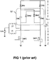
- FIG. 1 is a schematic diagram of the topology of the prior art circuit discussed above.
- capacitors CM1, CM2 and diodes DM1, DM2 form a multiplier stage (M1) which is integrated in boost converter with the possibility to increase several stages to achieve high gain.
- Two multiplier capacitors CM1, CM2 are connected with two multiplier diodes DM1, DM2 to form a multiplier stage M1.
- the diodes DS1 and DS2 are output diodes.
- Two power switches SW1, SW2 are connected in parallel.
- the number of multiplier stages is one.
- the voltage gain of this circuit is a function of duty ratio (D) and the number of multiplier cell (M).
- the static gain (Av) of the converter is shown in equation below, where M is the number of multiplier stages and D is duty ratio of the converter.
- Av M + 1 / 1 ⁇ D
- voltage stress across the power switches SW1, SW2 is proportional with duty ratio if the number of multiplier stage M is assumed to be constant.
- the novel approach proposed by embodiments of the present invention allows to increase the voltage gain range for a circuit having for example two multiplier stages to be from 2.66 to 12 for a duty-cycle range from 0.25 to 0.75.
- the inventors found that the above described limitation of prior art circuits can be overcome by introducing interchangeability between the different multiplier stages, as is done in DC-DC power converters according to embodiments of the present invention.
- the present invention therefore provides a novel structure which can interchange between different multiplier stages dynamically to provide a wider voltage gain range. This will help to operate intra-module converter within wide input voltage range, which will eventually facilitate to deal with varying output voltage of PV module due to (inter alia) partial shading.
- FIG. 2 shows an embodiment of a DC-DC power converter circuit according to the present invention, wherein two low frequency voltage controlled switches S1, S2 are connected between nodes of the two multiplier stages.
- switch S1 is connected in series with capacitor CM3 between input node in3 and output node on3, and switch S2 is connected in series with CM4 between input node in4 and output node on4.
- the "high-frequency" power switches SW1, SW2 would typically be operated at a constant frequency (for example about 50 kHz), but with a varying duty cycle ratio.
- the "low frequency” switches S1, S2 would typically be occasionally opened or closed.
- the high-frequency switches may be controlled by control signals c_SW1 and c_SW1, typically PWM signals, and the low-frequency switches S1, S2 may be controlled by signals c_S1 and c_S2, which may be generated by GPIO-pins (general-purpose input-output pins) of a controller 210, for example a programmable microcontroller.
- the controller may also use the output of the DC-DC power converter, (or a fraction thereof, as can be obtained for example from a voltage divider), as an input signal.
- the controller is provided with an algorithm that determines a suitable aspect ratio and that decides whether or not to bypass the second multiplier stage.
- the overall performance of the converter 200 and voltage stress across the power switches SW1, SW2 could be taken into account.
- the controller 210 may be part of the DC-DC power converter 200.
- the DC-DC-power converter 200 is designed and implemented in Spice to explore the feasibility of the converter.
- Real commercial model of MOSFETs and diodes have been used for all these simulations.
- the converter operation is in continuous conduction mode with 50 kHz operating frequency.
- Frequency of two voltage controlled switches S1, S2 is considered as 100 Hz for all the simulations (although in practice this would normally not be a periodic signal).
- 0.75 duty cycle it is possible to achieve a high voltage gain factor of 8 using only the first multiplier stage (S1, S2 closed), or a higher voltage gain of 12 when using both multiplier stages (S1, S2 open).
- the switches S1, S2 are added to the first multiplier stage, rather than to the second multiplier stage.
- the first switching device (S1) is connected in series with the first capacitor (CM1) between the first input node (in1) and the first output node (on1)
- the second switching device (S2) is connected in series with the second capacitor (CM2) between the second input node (in2) and the second output node (on2).
- input voltage is considered as 10V.
- V(S1), V(S3) are the signals provided to operate two switches S1 and S3 respectively. S1, S3 are simultaneously on the same switching state.
- Output voltage of the converter Vout, input voltage of the converter Vin and voltage across the low frequency switch VS1 are shown here. It is found that when S1 and S2 are closed, the output voltage is approximately 120V and when they are open the output voltage is about 80V.
- the stability of the waveform can be improved by implementing the control scheme. Overshoot of the output voltage at the start-up phase may also be controlled by the controller 210.
- the DC-DC power converter according to embodiments of the present invention provide a wider input voltage range which is advantageous to track the variations of output voltage of PV module dynamically.
- the overall performance of the PV system will be improved by applying the power converter of wider input voltage range since low voltage output of shaded solar cells (and the substrings they belong to) will also be added to the overall output power, rather than being simply ignored.
- the converter according to embodiments of the present invention helps to operate the converter in wider input voltage range by reducing voltage stress across the power switches SW1, SW2. It also helps to achieve best possible efficiency at a specific voltage gain by optimizing the usage of the number of multiplier stages based on duty cycle, voltage stress across power switches and power loss in diodes.
- FIG. 4 shows a schematic diagram of another embodiment of a DC-DC power converter according to the present invention, having four switches S1, S2, S3, S4 rather than only two.
- the idea is again to provide a DC-DC power convertor having a particular number of multiplier stages (implemented in hardware), but to allow to configure the topology to exchange between the multiplier stages dynamically based on the operating condition of the input voltage, e.g. the voltage Vdc provided by a PV module.
- four voltage controlled switches S1, S2, S3, and S4 are introduced in the circuit. These may be high-speed switches (e.g. power MOSFETs), but that is not required, because these switches would normally not be operated at high frequency. Therefore, low frequency switches such as for example electronic relays or solid state relays would also work.
- the converter will be operated with one multiplier stage or with two multiplier stages (or phrased differently: with one multiplier stage being bypassed, or not) by controlling these low frequency switches S1 to S4 at run time, for example by means of a controller 410.
- the switches S1 to S4 are connected between nodes of the two multiplier stages M1, M2.
- the four switches form two couples: a first couple formed by S1 and S2, and a second couple formed by S3 and S4.
- the switches within each couple have the same state, and the switches of different couples have different states.
- S1 and S2 are closed at the same time, and are open at the same time.
- S3 and S4 which are open or closed at the same time. in contrast, when S1 (and thus also S2) is closed, then S3 (and thus also S4) is open, and vice versa.
- the switches S1 and S2 are open, and the switches S3 and S4 are closed.
- the DC-DC power converter circuit of FIG. 4 is configured to act as a series connection of two multiplier stages M1 and M2. This mode can be used for example when a high voltage gain (for example Av>8) is needed.
- a second mode of operation the switches S1 and S2 are closed, and the switches S3 and S4 are open. In this mode, the second multiplier stage M2 is bypassed completely.
- This mode can be used for example when a low voltage gain (for example Av ⁇ 4) is needed.
- any of the first mode and second mode may be used, but the duty cycle would be different.
- the overall performance (e.g. power efficiency) of the converter 400 and/or voltage stress across the power switches SW1, SW2 may also be considered in order to determine the preferred number of multiplier stages to be used (or more precisely: whether to bypass the second multiplier stage, or not).
- the four low frequency switches S1, S2, S3, S4 are preferably controlled by a controller 410 at run time, based on voltage of the input voltage Vdc, for example the PV cells output or more accurately: the voltage of a PV substring (which is a series connection of PV cells).
- the converter will advantageously be working with wider voltage gain range by reducing voltage stress across the power switches SW1, SW2.
- DC-DC converter with wider input voltage range (in the example from 2.66 to 12) is advantageous to track the variations of the output voltage of PV modules dynamically over a wider range.
- the overall performance of the PV panel, and thus also the PV system comprising that PV panel will be improved, because the power originating from partially shaded substrings (causing a lower voltage output of the substring), would also be added to the output power, rather than being simply ignored, as is the case in many existing PV panels having a so called "bypass diode".
- the proposed converter according to embodiments of the invention advantageously helps to operate the converter in wider input voltage range. It also helps to achieve best possible efficiency at a specific voltage gain by optimizing the usage of the number of multiplier stages based on duty cycle, voltage stress across power switches and power loss in diodes.
- Another benefit of the DC-DC power converter of FIG. 4 is that not all the passive components are in use all the time. Because when the module is fully illuminated, the lower voltage gain is required, thus one multiplier stage will be bypassed.
- the proposed converter 400 comprising four switches S1-S4, is designed and implemented in Spice to explore the feasibility of the converter.
- Real commercial model of MOSFETs and diodes have been used for all these simulation.
- the converter operation is in continuous conduction mode with the power switches being operated at 50 kHz operating frequency.
- the four low-frequency switches S1-S4 would normally not be operated periodically, but depending for example on whether the input voltage Vdc is low or high, for the purpose of the simulation, these switches were operated with a frequency of 100 Hz for all the simulations.
- 0.75 duty cycle it is possible to selectively achieve a high voltage gain of 8 with only a single multiplier stage (second mode of the converter), but also a higher voltage gain of 12 when using both multiplier stages (first mode of the converter).
- the position of the first and second multiplier stage M1, M2 are swapped, or in other words, the switch S1 would be arranged between node X and node on1, the switch S2 would be arranged between node Y and node on2, the switch S3 would be arranged between node X and node in1, and the switch S4 would be arranged between node Y and node in2.
- This circuit would behave similar to the circuit shown in FIG. 4 , and offer the same advantages, except that in this case, of course, the first multiplier stage M1 can be bypassed, or not.
- FIG. 5 shows a variant of the DC-DC power converter of FIG. 4 .
- Everything described for the converter of FIG. 4 is also applicable for the converter of FIG. 5 .
- the circuit of FIG. 5 is configurable in a first mode (S1 and S2 open, S3 and S4 closed) wherein the two multiplier stages are connected in series, and both contribute to the output voltage multiplication; or in a second mode (S1 and S2 closed, S3 and S4 open wherein the second multiplier stage is completely bypassed, and does not contribute to the overall voltage multiplication.
- S1 and S2 open, S3 and S4 closed wherein the second multiplier stage is completely bypassed, and does not contribute to the overall voltage multiplication.
- the relative position of the diode DM3 and the switch S3 could be interchanged.
- the relative position of the diode DM4 and the switch S4 could be interchanged.
- the position of the first and second multiplier stage M1, M2 are swapped, or in other words, the switch S1 would be arranged between node X and node on1, the switch S2 would be arranged between node Y and node on1, the switch S3 would be arranged in series with diode DM1 between node in1 and node on2, and the switch S4 would be arranged in series with diode DM2 between node Y and node on1.
- This circuit would behave similar to the circuit shown in FIG. 5 , and offer the same advantages, except that in this case, of course, the first multiplier stage M1 can be bypassed, or not.
- FIG. 6 shows another variant of the DC-DC power converter of FIG. 4 .
- Everything described for the converter of FIG. 4 is also applicable for the converter of FIG. 6 .
- the circuit of FIG. 6 is configurable in a first mode (S1 and S2 open, S3 and S4 closed) wherein the two multiplier stages are connected in series, and both contribute to the output voltage multiplication; or in a second mode (S1 and S2 closed, S3 and S4 open wherein the second multiplier stage is completely bypassed, and does not contribute to the overall voltage multiplication.
- the position of the first and second multiplier stage M1, M2 are swapped, or in other words, the switch S1 would be arranged between node X and node on2, the switch S2 would be arranged between node Y and node on1, the switch S3 would be arranged between node X and node in1, and the switch S4 would be arranged between node Y and node in2.
- This circuit would behave similar to the circuit shown in FIG. 6 , and offer the same advantages, except that in this case, of course, the first multiplier stage M1 can be bypassed, or not.
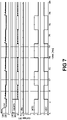
- V(S1) is the signal provided to operate the switches S1 and S2
- V(S3) is the signal to operate the switches S3 and S4.
- Output voltage of the converter Vout, input voltage of the converter Vin and voltage across the multiplier capacitor V(CM3) are shown.
- the stability of the waveform may be improved by implementing a control scheme. Overshoot of the output voltage at the start-up phase may also be controlled by the controller.
- FIG. 8 shows simulated current waveforms of the DC-DC converter of FIG. 4 .
- the input voltage and the duty cycle are kept same for this simulation as well.
- the control signal V(S1) for the switches S1 and S2 and the control signal V(S3) for the switches S3 and S4, , the current of the two inductors I(L1), I(L2) and the current I(CM3) of the multiplier capacitor CM3 are shown.
- the simulated current waveforms are presented to verify the functionality of the converter. It is seen that two inductor currents follow the interchangeability between the multiplier stages.
- the proposed converter advantageously is able to interchange between multiplier stages dynamically and eventually make voltage gain range wider which is useful to operate the converter in wide input voltage range.
- the DC-DC power converters described above all have an increased voltage gain range, and can advantageously be used in PV applications, especially as an intra-module converter.
- Embodiments of the present invention provide a novel approach to deal with the fluctuation of the output voltage of the PV substrings more efficiently by increasing voltage gain range and eventually increasing input voltage range of the DC-DC converter. Moreover, there are benefits in providing a wider input voltage range for a DC-DC converter in the PV application.
- Embodiments of the present invention advantageously provide a novel approach to deal with the fluctuation of the output voltage of the PV substrings more efficiently by increasing voltage gain range and eventually increasing input voltage range of a non-isolated DC-DC converter.
- Advantageously embodiments of the present invention provide ultra-wide gain range auto-reconfigurable non-isolated DC-DC converters.
- the value of input parameters the DC-DC converter according to the invention can be changed according to requirement. If for instance one wants to use the converter at module level, then the input voltage range is preferably higher than when it is used as an intra-module converter. Output voltage can also be changed accordingly.
- the input voltage range in embodiments without auto-reconfigurable approach, can be between 30 to 78 V, whereas the voltage gain rage is between 12 to 4.6.
- the input voltage can be between 30 to 116 V, with a voltage grain range of 12 to 3.1.
- the optimum duty cycle range is preferably between 0.75 and 0.35. Therefore, we can see in this approach that basically voltage gain range is increased in an optimum duty cycle range without compromising efficiency. Now, based on the voltage gain range the input and output voltage range can be varied as per the requirement.
Landscapes
- Engineering & Computer Science (AREA)
- Power Engineering (AREA)
- Dc-Dc Converters (AREA)
Claims (9)
- Une unité photovoltaïque comprenant :- au moins deux sous-chaînes connectées en parallèle, chaque sous-chaîne comprenant une pluralité de cellules solaires connectées en série, et chaque sous-chaîne comprenant au moins un convertisseur de courant CC-CC connecté en série avec la connexion en série des cellules solaires configuré pour fonctionner comme un convertisseur de courant CC-CC intra-module ; ou- au moins un convertisseur de courant CC-CC configuré pour fonctionner comme un convertisseur de courant CC-CC de niveau de module ;dans laquelle le convertisseur de courant CC-CC (200, 400, 500, 600) comprend :- au moins deux étages multiplicateurs (M1, M2), chaque étage multiplicateur comprenant deux condensateurs (CM1, CM2 ; CM3, CM4), chaque condensateur étant respectivement connecté à une diode (DM2, DM1 ; DM4, DM3), lesdites diodes étant adaptées pour charger les condensateurs (CM1, CM2 ; CM3, CM4) avec une tension,- le premier étage multiplicateur (M1) comprenant :caractérisée par l'une des alternatives suivantes :- un premier et un deuxième nœud d'entrée (in1, in2) et un premier et un deuxième nœud de sortie (on1, on2) ; et- un premier condensateur (CM1) connecté entre le premier nœud d'entrée (in1) et le premier nœud de sortie (on1), et un deuxième condensateur (CM2) connecté entre le deuxième nœud d'entrée (in2) et le deuxième nœud de sortie (on2) ; et- une première diode (DM1) connectée par son anode au premier nœud d'entrée (in1) et par sa cathode au deuxième nœud de sortie (on2), et une deuxième diode (DM2) connectée par son anode au deuxième nœud d'entrée (in2) et par sa cathode au premier nœud de sortie (on1) ;- le second étage multiplicateur (M2) comprenant :- un troisième et un quatrième nœud d'entrée (in3, in4) et un troisième et un quatrième nœud de sortie (on3, on4) ; et- un troisième condensateur (CM3) connecté entre le troisième nœud d'entrée (in3) et le troisième nœud de sortie (on3), et un quatrième condensateur (CM4) connecté entre le quatrième nœud d'entrée (in4) et le quatrième nœud de sortie (on4) ; et- une troisième diode (DM3) connectée par son anode au troisième nœud d'entrée (in3) et par sa cathode au quatrième nœud de sortie (on4), et une quatrième diode (DM4) connectée par son anode au quatrième nœud d'entrée (in4) et par sa cathode au troisième nœud de sortie (on3) ;- le premier nœud de sortie (on1) étant connecté au troisième nœud d'entrée (in3) et le deuxième nœud de sortie (on2) étant connecté au quatrième nœud d'entrée (in4) ;- au moins deux dispositifs de commutation (S1, S2), dans laquelle lesdits au moins deux dispositifs de commutation (S1, S2) sont agencés pour connecter sélectivement les au moins deux étages multiplicateurs (M1, M2) en série dans un premier mode de fonctionnement et pour dériver au moins partiellement l'un des au moins deux étages multiplicateurs (M2) dans un second mode de fonctionnement, en augmentant ainsi une plage de gain de tension du convertisseur de courant CC-CC,- le premier dispositif de commutation (S1) est connecté en série avec le premier condensateur (CM1) entre le premier nœud d'entrée (in1) et le premier nœud de sortie (on1), et le deuxième dispositif de commutation (S2) est connecté en série avec le deuxième condensateur (CM2) entre le deuxième nœud d'entrée (in2) et le deuxième nœud de sortie (on2), ou- le premier dispositif de commutation (S1) est connecté en série avec le troisième condensateur (CM3) entre le troisième nœud d'entrée (in3) et le troisième nœud de sortie (on3), et le deuxième dispositif de commutation (S2) est connecté en série avec le quatrième condensateur (CM4) entre le quatrième nœud d'entrée (in4) et le quatrième nœud de sortie (on4), ou- le convertisseur de courant CC-CC (400) comprend en outre un troisième et un quatrième dispositif de commutation (S3, S4), et l'une des alternatives suivantes :a) dans laquelle le premier dispositif de commutation (S1) est connecté entre le premier nœud de sortie (on1) et le troisième nœud de sortie (on3), et le deuxième dispositif de commutation (S2) est connecté entre le deuxième nœud de sortie (on2) et le quatrième nœud de sortie (on4), et le troisième dispositif de commutation (S3) est connecté entre le premier nœud de sortie (on1) et le troisième nœud d'entrée (in3), et le quatrième dispositif de commutation (S4) est connecté entre le deuxième nœud de sortie (on2) et le quatrième nœud d'entrée (in4) ;b) dans laquelle le premier dispositif de commutation (S1) est connecté entre le premier nœud de sortie (on1) et le troisième nœud de sortie (on3), et le deuxième dispositif de commutation (S2) est connecté entre le deuxième nœud de sortie (on2) et le quatrième nœud de sortie (on4), et le troisième dispositif de commutation (S3) est connecté en série avec la troisième diode (DM3) entre le troisième nœud d'entrée (in3) et le quatrième nœud de sortie (on4), et le quatrième dispositif de commutation (S4) est connecté en série avec la quatrième diode (DM4) entre la quatrième entrée (in4) et le troisième nœud de sortie (on3) ;c) dans laquelle le premier dispositif de commutation (S1) est connecté entre le premier nœud de sortie (onl) et le quatrième nœud de sortie (on4), et le deuxième dispositif de commutation (S2) est connecté entre le deuxième nœud de sortie (on2) et le troisième nœud de sortie (on3), et le troisième dispositif de commutation (S3) est connecté entre le premier nœud de sortie (onl) et le troisième nœud d'entrée (in3) et le quatrième dispositif de commutation (S4) est connecté entre le deuxième nœud de sortie (on2) et le quatrième nœud d'entrée (in4).
- L'unité photovoltaïque selon la revendication 1, dans laquelle le convertisseur de courant CC-CC (200, 400, 500, 600) comprend en outre :- une première diode de protection (DS1) connectée par son anode à un premier nœud de sortie (on3) du second étage multiplicateur (M2) et par sa cathode à un nœud de sortie (out) du convertisseur CC-CC ; et- une deuxième diode de protection (DS2) connectée par son anode à un deuxième nœud de sortie (on4) du second étage multiplicateur (M2) et par son anode au nœud de sortie (out) du convertisseur de courant CC-CC ; et- un condensateur de sortie (Co) connecté entre un nœud de masse (gnd) du convertisseur CC-CC et le nœud de sortie (out) du convertisseur de courant CC-CC.
- L'unité photovoltaïque selon une quelconque revendication précédente, dans laquelle le convertisseur de courant CC-CC (200, 400, 500, 600) comprend en outre :- un premier commutateur de courant (SW1) agencé entre le nœud de masse (gnd) et un premier nœud d'entrée (in1) du premier étage multiplicateur (M1) et adapté pour tirer un premier courant (i1) à travers une première inductance (L1) pouvant être connectée audit premier nœud d'entrée (in1) ;- un deuxième commutateur de courant (SW2) agencé entre le nœud de masse (gnd) et un deuxième nœud d'entrée (in2) du premier étage multiplicateur (M1) et adapté pour tirer un deuxième courant (i2) à travers une seconde inductance (L2) pouvant être connectée audit deuxième nœud d'entrée (in2).
- L'unité photovoltaïque selon une quelconque revendication précédente, dans laquelle les au moins deux dispositifs de commutation (S1, S2 ; S3, S4) sont adaptés pour fonctionner à une fréquence inférieure à la fréquence des commutateurs de courant (SW1, SW2) et/ou dans laquelle les au moins deux dispositifs de commutation (S1, S2 ; S3, S4) sont des relais électriques ou des relais statiques.
- L'unité photovoltaïque selon une quelconque revendication précédente, dans laquelle le convertisseur de courant CC-CC comprend en outre ladite première inductance (L1) connectée au premier nœud d'entrée (in1) et comprenant la seconde inductance (L2) connectée au deuxième nœud d'entrée (in2).
- L'unité photovoltaïque selon une quelconque revendication précédente,dans laquelle le convertisseur de courant CC-CC est un convertisseur de courant non isolé, oudans laquelle le convertisseur de courant CC-CC est un convertisseur de courant élévateur.
- L'unité photovoltaïque selon une quelconque revendication précédente, comprenant en outre un dispositif de commande adapté pour ouvrir et fermer sélectivement les au moins deux dispositifs de commutation (S1, S2 ; S3, S4), et/ou dans laquelle le dispositif de commande est en outre adapté pour déterminer un cycle de service, et pour générer un signal de commande avec le cycle de service déterminé, et pour appliquer le signal de commande aux premier et deuxième commutateurs de courant (SW1, SW2).
- Un système d'alimentation pour commander une pluralité d'unités photovoltaïques, le système d'alimentation comprenant :- une première unité photovoltaïque (PU1) selon une quelconque revendication précédente, adaptée pour générer une première tension ;- une seconde unité photovoltaïque (PU2) selon une quelconque revendication précédente, adaptée pour générer une seconde tension ;- la première unité photovoltaïque (PU1) et la seconde unité photovoltaïque (PU2) étant connectées en parallèle ou en série ;- un dispositif de commande adapté pour commander la première tension (V1) et la seconde tension (V2) ;et/ou dans lequel le système d'alimentation comprend en outre un onduleur configuré pour convertir le courant CC généré par la première et la seconde unité photovoltaïque (PU1, PU2) et pour injecter le courant convertie dans un réseau public.
- Procédé de fabrication d'un convertisseur de courant CC-CC (200, 400, 500, 600), comprenant les étapes consistant à :- fournir un premier étage multiplicateur (M1) comprenant :fournir en outre un troisième et un quatrième dispositif de commutation (S3, S4), et l'une des alternatives suivantes :- un premier et un deuxième nœud d'entrée (in1, in2) et un premier et un deuxième nœud de sortie (on1, on2) ; et- un premier condensateur (CM1) connecté entre le premier nœud d'entrée (in1) et le premier nœud de sortie (on1), et un deuxième condensateur (CM2) connecté entre le deuxième nœud d'entrée (in2) et le deuxième nœud de sortie (on2) ; et- une première diode (DM1) connectée par son anode au premier nœud d'entrée (in1) et par sa cathode au deuxième nœud de sortie (on2), et une deuxième diode (DM2) connectée par son anode au deuxième nœud d'entrée (in2) et par sa cathode au premier nœud de sortie (on1) ;- fournir un second étage multiplicateur (M2) comprenant :- un troisième et un quatrième nœud d'entrée (in3, in4) et un troisième et un quatrième nœud de sortie (on3, on4) ; et- un troisième condensateur (CM3) connecté entre le troisième nœud d'entrée (in3) et le troisième nœud de sortie (on3), et un quatrième condensateur (CM4) connecté entre le quatrième nœud d'entrée (in4) et le quatrième nœud de sortie (on4) ; et- une troisième diode (DM3) connectée par son anode au troisième nœud d'entrée (in3) et par sa cathode au quatrième nœud de sortie (on4), et une quatrième diode (DM4) connectée par son anode au quatrième nœud d'entrée (in4) et par sa cathode au troisième nœud de sortie (on3) ;- connecter le premier étage multiplicateur (M1) au second étage multiplicateur (M2) en connectant le premier nœud de sortie (on1) au troisième nœud d'entrée (in3) et en connectant le deuxième nœud de sortie (on2) au quatrième nœud d'entrée (in4) ;- ajouter au moins un premier et un deuxième dispositif de commutation (S1, S2) au premier étage multiplicateur (M1) ou au second étage multiplicateur (M2) pour dériver au moins partiellement le premier ou le second étage multiplicateur (M1, M2), en augmentant ainsi la plage de gain de tension du convertisseur de courant CC-CC, par l'une des alternatives suivantes :- connecter le premier dispositif de commutation (S1) en série avec le premier condensateur (CM1) entre le premier nœud d'entrée (in1) et le premier nœud de sortie (on1), et connecter le deuxième dispositif de commutation (S2) en série avec le deuxième condensateur (CM2) entre le deuxième nœud d'entrée (in2) et le deuxième nœud de sortie (on2), ou- connecter le premier dispositif de commutation (S1) en série avec le troisième condensateur (CM3) entre le troisième nœud d'entrée (in3) et le troisième nœud de sortie (on3), et connecter le deuxième dispositif de commutation (S2) en série avec le quatrième condensateur (CM4) entre le quatrième nœud d'entrée (in4) et le quatrième nœud de sortie (on4) ; oua) connecter le premier dispositif de commutation (S1) entre le premier nœud de sortie (on1) et le troisième nœud de sortie (on3), et connecter le deuxième dispositif de commutation (S2) entre le deuxième nœud de sortie (on2) et le quatrième nœud de sortie (on4), et connecter le troisième dispositif de commutation (S3) entre le premier nœud de sortie (on1) et le troisième nœud d'entrée (in3) et connecter le quatrième dispositif de commutation (S4) entre le deuxième nœud de sortie (on2) et le quatrième nœud d'entrée (in4) ;b) connecter le premier dispositif de commutation (S1) entre le premier nœud de sortie (on1) et le troisième nœud de sortie (on3), et connecter le deuxième dispositif de commutation (S2) entre le deuxième nœud de sortie (on2) au quatrième nœud de sortie (on4), et connecter le troisième dispositif de commutation (S3) en série avec la troisième diode (DM3) entre le troisième nœud d'entrée (in3), et connecter le quatrième nœud de sortie (on4) et le quatrième dispositif de commutation (S4) en série avec la quatrième diode (DM4) entre le quatrième nœud d'entrée (in4) et le troisième nœud de sortie (on3) ;c) connecter le premier dispositif de commutation (S1) entre le premier nœud de sortie (on1) et le quatrième nœud de sortie (on4), et connecter le deuxième dispositif de commutation (S2) entre le deuxième nœud de sortie (on2) et le troisième nœud de sortie (on3), et connecter le troisième dispositif de commutation (S3) entre le premier nœud de sortie (on1) et le troisième nœud d'entrée (in3), et connecter le quatrième dispositif de commutation (S4) entre le deuxième nœud de sortie (on2) et le quatrième nœud d'entrée (in4).
Applications Claiming Priority (2)
| Application Number | Priority Date | Filing Date | Title |
|---|---|---|---|
| GBGB1411022.5A GB201411022D0 (en) | 2014-06-20 | 2014-06-20 | Methods and devices for increasing the voltage gain range of a DC-DC power converter |
| PCT/EP2015/064001 WO2015193510A1 (fr) | 2014-06-20 | 2015-06-22 | Procédés et dispositifs pour augmenter la plage de gain en tension d'un convertisseur de courant continu-continu |
Publications (2)
| Publication Number | Publication Date |
|---|---|
| EP3158632A1 EP3158632A1 (fr) | 2017-04-26 |
| EP3158632B1 true EP3158632B1 (fr) | 2022-10-12 |
Family
ID=51409898
Family Applications (1)
| Application Number | Title | Priority Date | Filing Date |
|---|---|---|---|
| EP15730506.1A Active EP3158632B1 (fr) | 2014-06-20 | 2015-06-22 | Procédés et dispositifs pour augmenter la plage de gain en tension d'un convertisseur de courant continu-continu |
Country Status (4)
| Country | Link |
|---|---|
| US (1) | US10530162B2 (fr) |
| EP (1) | EP3158632B1 (fr) |
| GB (1) | GB201411022D0 (fr) |
| WO (1) | WO2015193510A1 (fr) |
Families Citing this family (5)
| Publication number | Priority date | Publication date | Assignee | Title |
|---|---|---|---|---|
| CN112737332B (zh) * | 2020-12-25 | 2022-02-08 | 三峡大学 | 一种自动均压双极性Cuk DC-DC变换器 |
| CN112737331B (zh) * | 2020-12-25 | 2022-02-08 | 三峡大学 | 一种自动均压双极性buck-boost DC-DC变换器 |
| CN112737324B (zh) * | 2020-12-25 | 2022-02-01 | 三峡大学 | 一种自动均压双极性Zeta DC-DC变换器 |
| CN114726215B (zh) * | 2022-04-19 | 2022-11-08 | 广东工业大学 | 一种田字型阻抗网络软开关高增益升压变换器 |
| US12088247B2 (en) | 2022-05-20 | 2024-09-10 | Inergy Holdings, Llc. | Modular photovoltaic power production system |
Citations (1)
| Publication number | Priority date | Publication date | Assignee | Title |
|---|---|---|---|---|
| US20140022005A1 (en) * | 2012-07-23 | 2014-01-23 | Freescale Semiconductor, Inc. | Configurable multistage charge pump using a supply detect scheme |
Family Cites Families (6)
| Publication number | Priority date | Publication date | Assignee | Title |
|---|---|---|---|---|
| US6563235B1 (en) * | 2000-10-03 | 2003-05-13 | National Semiconductor Corporation | Switched capacitor array circuit for use in DC-DC converter and method |
| US7602232B2 (en) * | 2005-11-01 | 2009-10-13 | Semiconductor Components Industries, L.L.C. | Programmable fractional charge pump for DC-DC converter |
| US8473250B2 (en) * | 2006-12-06 | 2013-06-25 | Solaredge, Ltd. | Monitoring of distributed power harvesting systems using DC power sources |
| TWI429176B (zh) | 2011-03-31 | 2014-03-01 | Nat Univ Tsing Hua | 高升壓比直流轉換器 |
| CN102969893B (zh) * | 2012-12-12 | 2015-09-30 | 重庆大学 | 一种高增益升压型直流变换器 |
| US9524832B2 (en) * | 2013-03-15 | 2016-12-20 | Solantro Semiconductor Corp | Intelligent safety disconnect switching |
-
2014
- 2014-06-20 GB GBGB1411022.5A patent/GB201411022D0/en not_active Ceased
-
2015
- 2015-06-22 US US15/319,828 patent/US10530162B2/en active Active
- 2015-06-22 WO PCT/EP2015/064001 patent/WO2015193510A1/fr not_active Ceased
- 2015-06-22 EP EP15730506.1A patent/EP3158632B1/fr active Active
Patent Citations (1)
| Publication number | Priority date | Publication date | Assignee | Title |
|---|---|---|---|---|
| US20140022005A1 (en) * | 2012-07-23 | 2014-01-23 | Freescale Semiconductor, Inc. | Configurable multistage charge pump using a supply detect scheme |
Non-Patent Citations (1)
| Title |
|---|
| TOFOLI F L ET AL: "Novel Nonisolated High-Voltage Gain DC DC Converters Based on 3SSC and VMC", IEEE TRANSACTIONS ON POWER ELECTRONICS, INSTITUTE OF ELECTRICAL AND ELECTRONICS ENGINEERS, USA, vol. 27, no. 9, 1 September 2012 (2012-09-01), pages 3897 - 3907, XP011454766, ISSN: 0885-8993, DOI: 10.1109/TPEL.2012.2190943 * |
Also Published As
| Publication number | Publication date |
|---|---|
| EP3158632A1 (fr) | 2017-04-26 |
| US10530162B2 (en) | 2020-01-07 |
| WO2015193510A1 (fr) | 2015-12-23 |
| GB201411022D0 (en) | 2014-08-06 |
| US20170133853A1 (en) | 2017-05-11 |
Similar Documents
| Publication | Publication Date | Title |
|---|---|---|
| Rosas-Caro et al. | A DC–DC multilevel boost converter | |
| Zhang et al. | A 3-Z-network boost converter | |
| Zhou et al. | High step-up converter with capacity of multiple input | |
| CN101888734B (zh) | 带升/降压功率因数校正dc-dc转换器的电子镇流器 | |
| EP3050202B1 (fr) | Convertisseur cc-cc intra-module et module photovoltaïque le comprenant | |
| EP3158632B1 (fr) | Procédés et dispositifs pour augmenter la plage de gain en tension d'un convertisseur de courant continu-continu | |
| Torrico-Bascopé et al. | A generalized high voltage gain boost converter based on three-state switching cell | |
| Ho et al. | Embedded quasi-Z-source inverters based on active switched-capacitor structure | |
| Priya et al. | Comparison of n-stage cascade cockcroft-walton voltage multiplier applied to transformer-less dc-dc boost converter | |
| CN106787736B (zh) | 一种双开关高升压比pwm直流变换器 | |
| Sridharan et al. | Wide boost ratio in quasi-impedance network converter using switch voltage spike reduction technique | |
| KR100898259B1 (ko) | 전하 펌프 방식의 전력 변환 인버터 | |
| Lavanya et al. | Dual input DC-DC converter for renewable energy systems | |
| Dineshkumar et al. | Design of boost inverter for solar power based stand alone systems | |
| Babu et al. | Novel Single-Stage Transformer-less Cascaded Differential Boost Single-Phase PV Inverter for Grid-Tied Applications | |
| Zengin et al. | Evaluation of two-stage soft-switched flyback micro-inverter for photovoltaic applications | |
| Srinithi et al. | Symmetric multilevel inverter using DC-DC zeta converter | |
| Chander et al. | Dual input converter fed transformerless multilevel inverter for standalone PV application | |
| Aleem et al. | Single-phase isolated impedance-source inverters | |
| Khan et al. | Hybrid split pi converter | |
| Ayswarya et al. | Leakage current suppression for transformerless inverter for grid connected PV power systems | |
| Sriramalakshmi et al. | Single-stage boost inverter topologies for nanogrid applications | |
| SCHEME | Single phase multilevel inverter based on a novel switching scheme using buck converter | |
| Ismeil et al. | Single-phase cascaded semi-Z-source inverter for photovoltaic applications | |
| Michal | Series capacitor dual-output DC/DC converter and power inverter with reduced switching voltage and stress on switching devices |
Legal Events
| Date | Code | Title | Description |
|---|---|---|---|
| STAA | Information on the status of an ep patent application or granted ep patent |
Free format text: STATUS: THE INTERNATIONAL PUBLICATION HAS BEEN MADE |
|
| PUAI | Public reference made under article 153(3) epc to a published international application that has entered the european phase |
Free format text: ORIGINAL CODE: 0009012 |
|
| STAA | Information on the status of an ep patent application or granted ep patent |
Free format text: STATUS: REQUEST FOR EXAMINATION WAS MADE |
|
| 17P | Request for examination filed |
Effective date: 20170113 |
|
| AK | Designated contracting states |
Kind code of ref document: A1 Designated state(s): AL AT BE BG CH CY CZ DE DK EE ES FI FR GB GR HR HU IE IS IT LI LT LU LV MC MK MT NL NO PL PT RO RS SE SI SK SM TR |
|
| AX | Request for extension of the european patent |
Extension state: BA ME |
|
| DAV | Request for validation of the european patent (deleted) | ||
| DAX | Request for extension of the european patent (deleted) | ||
| STAA | Information on the status of an ep patent application or granted ep patent |
Free format text: STATUS: EXAMINATION IS IN PROGRESS |
|
| 17Q | First examination report despatched |
Effective date: 20190408 |
|
| GRAP | Despatch of communication of intention to grant a patent |
Free format text: ORIGINAL CODE: EPIDOSNIGR1 |
|
| STAA | Information on the status of an ep patent application or granted ep patent |
Free format text: STATUS: GRANT OF PATENT IS INTENDED |
|
| INTG | Intention to grant announced |
Effective date: 20220425 |
|
| GRAS | Grant fee paid |
Free format text: ORIGINAL CODE: EPIDOSNIGR3 |
|
| GRAA | (expected) grant |
Free format text: ORIGINAL CODE: 0009210 |
|
| STAA | Information on the status of an ep patent application or granted ep patent |
Free format text: STATUS: THE PATENT HAS BEEN GRANTED |
|
| AK | Designated contracting states |
Kind code of ref document: B1 Designated state(s): AL AT BE BG CH CY CZ DE DK EE ES FI FR GB GR HR HU IE IS IT LI LT LU LV MC MK MT NL NO PL PT RO RS SE SI SK SM TR |
|
| REG | Reference to a national code |
Ref country code: GB Ref legal event code: FG4D |
|
| REG | Reference to a national code |
Ref country code: CH Ref legal event code: EP |
|
| REG | Reference to a national code |
Ref country code: DE Ref legal event code: R096 Ref document number: 602015081154 Country of ref document: DE |
|
| REG | Reference to a national code |
Ref country code: IE Ref legal event code: FG4D |
|
| REG | Reference to a national code |
Ref country code: AT Ref legal event code: REF Ref document number: 1524766 Country of ref document: AT Kind code of ref document: T Effective date: 20221115 |
|
| REG | Reference to a national code |
Ref country code: NL Ref legal event code: FP |
|
| REG | Reference to a national code |
Ref country code: LT Ref legal event code: MG9D |
|
| REG | Reference to a national code |
Ref country code: AT Ref legal event code: MK05 Ref document number: 1524766 Country of ref document: AT Kind code of ref document: T Effective date: 20221012 |
|
| PG25 | Lapsed in a contracting state [announced via postgrant information from national office to epo] |
Ref country code: SE Free format text: LAPSE BECAUSE OF FAILURE TO SUBMIT A TRANSLATION OF THE DESCRIPTION OR TO PAY THE FEE WITHIN THE PRESCRIBED TIME-LIMIT Effective date: 20221012 Ref country code: PT Free format text: LAPSE BECAUSE OF FAILURE TO SUBMIT A TRANSLATION OF THE DESCRIPTION OR TO PAY THE FEE WITHIN THE PRESCRIBED TIME-LIMIT Effective date: 20230213 Ref country code: NO Free format text: LAPSE BECAUSE OF FAILURE TO SUBMIT A TRANSLATION OF THE DESCRIPTION OR TO PAY THE FEE WITHIN THE PRESCRIBED TIME-LIMIT Effective date: 20230112 Ref country code: LT Free format text: LAPSE BECAUSE OF FAILURE TO SUBMIT A TRANSLATION OF THE DESCRIPTION OR TO PAY THE FEE WITHIN THE PRESCRIBED TIME-LIMIT Effective date: 20221012 Ref country code: FI Free format text: LAPSE BECAUSE OF FAILURE TO SUBMIT A TRANSLATION OF THE DESCRIPTION OR TO PAY THE FEE WITHIN THE PRESCRIBED TIME-LIMIT Effective date: 20221012 Ref country code: ES Free format text: LAPSE BECAUSE OF FAILURE TO SUBMIT A TRANSLATION OF THE DESCRIPTION OR TO PAY THE FEE WITHIN THE PRESCRIBED TIME-LIMIT Effective date: 20221012 Ref country code: AT Free format text: LAPSE BECAUSE OF FAILURE TO SUBMIT A TRANSLATION OF THE DESCRIPTION OR TO PAY THE FEE WITHIN THE PRESCRIBED TIME-LIMIT Effective date: 20221012 |
|
| PG25 | Lapsed in a contracting state [announced via postgrant information from national office to epo] |
Ref country code: RS Free format text: LAPSE BECAUSE OF FAILURE TO SUBMIT A TRANSLATION OF THE DESCRIPTION OR TO PAY THE FEE WITHIN THE PRESCRIBED TIME-LIMIT Effective date: 20221012 Ref country code: PL Free format text: LAPSE BECAUSE OF FAILURE TO SUBMIT A TRANSLATION OF THE DESCRIPTION OR TO PAY THE FEE WITHIN THE PRESCRIBED TIME-LIMIT Effective date: 20221012 Ref country code: LV Free format text: LAPSE BECAUSE OF FAILURE TO SUBMIT A TRANSLATION OF THE DESCRIPTION OR TO PAY THE FEE WITHIN THE PRESCRIBED TIME-LIMIT Effective date: 20221012 Ref country code: IS Free format text: LAPSE BECAUSE OF FAILURE TO SUBMIT A TRANSLATION OF THE DESCRIPTION OR TO PAY THE FEE WITHIN THE PRESCRIBED TIME-LIMIT Effective date: 20230212 Ref country code: HR Free format text: LAPSE BECAUSE OF FAILURE TO SUBMIT A TRANSLATION OF THE DESCRIPTION OR TO PAY THE FEE WITHIN THE PRESCRIBED TIME-LIMIT Effective date: 20221012 Ref country code: GR Free format text: LAPSE BECAUSE OF FAILURE TO SUBMIT A TRANSLATION OF THE DESCRIPTION OR TO PAY THE FEE WITHIN THE PRESCRIBED TIME-LIMIT Effective date: 20230113 |
|
| P01 | Opt-out of the competence of the unified patent court (upc) registered |
Effective date: 20230526 |
|
| REG | Reference to a national code |
Ref country code: DE Ref legal event code: R097 Ref document number: 602015081154 Country of ref document: DE |
|
| PG25 | Lapsed in a contracting state [announced via postgrant information from national office to epo] |
Ref country code: SM Free format text: LAPSE BECAUSE OF FAILURE TO SUBMIT A TRANSLATION OF THE DESCRIPTION OR TO PAY THE FEE WITHIN THE PRESCRIBED TIME-LIMIT Effective date: 20221012 Ref country code: RO Free format text: LAPSE BECAUSE OF FAILURE TO SUBMIT A TRANSLATION OF THE DESCRIPTION OR TO PAY THE FEE WITHIN THE PRESCRIBED TIME-LIMIT Effective date: 20221012 Ref country code: EE Free format text: LAPSE BECAUSE OF FAILURE TO SUBMIT A TRANSLATION OF THE DESCRIPTION OR TO PAY THE FEE WITHIN THE PRESCRIBED TIME-LIMIT Effective date: 20221012 Ref country code: DK Free format text: LAPSE BECAUSE OF FAILURE TO SUBMIT A TRANSLATION OF THE DESCRIPTION OR TO PAY THE FEE WITHIN THE PRESCRIBED TIME-LIMIT Effective date: 20221012 Ref country code: CZ Free format text: LAPSE BECAUSE OF FAILURE TO SUBMIT A TRANSLATION OF THE DESCRIPTION OR TO PAY THE FEE WITHIN THE PRESCRIBED TIME-LIMIT Effective date: 20221012 |
|
| PLBE | No opposition filed within time limit |
Free format text: ORIGINAL CODE: 0009261 |
|
| STAA | Information on the status of an ep patent application or granted ep patent |
Free format text: STATUS: NO OPPOSITION FILED WITHIN TIME LIMIT |
|
| PG25 | Lapsed in a contracting state [announced via postgrant information from national office to epo] |
Ref country code: SK Free format text: LAPSE BECAUSE OF FAILURE TO SUBMIT A TRANSLATION OF THE DESCRIPTION OR TO PAY THE FEE WITHIN THE PRESCRIBED TIME-LIMIT Effective date: 20221012 Ref country code: AL Free format text: LAPSE BECAUSE OF FAILURE TO SUBMIT A TRANSLATION OF THE DESCRIPTION OR TO PAY THE FEE WITHIN THE PRESCRIBED TIME-LIMIT Effective date: 20221012 |
|
| 26N | No opposition filed |
Effective date: 20230713 |
|
| PG25 | Lapsed in a contracting state [announced via postgrant information from national office to epo] |
Ref country code: SI Free format text: LAPSE BECAUSE OF FAILURE TO SUBMIT A TRANSLATION OF THE DESCRIPTION OR TO PAY THE FEE WITHIN THE PRESCRIBED TIME-LIMIT Effective date: 20221012 |
|
| PG25 | Lapsed in a contracting state [announced via postgrant information from national office to epo] |
Ref country code: MC Free format text: LAPSE BECAUSE OF FAILURE TO SUBMIT A TRANSLATION OF THE DESCRIPTION OR TO PAY THE FEE WITHIN THE PRESCRIBED TIME-LIMIT Effective date: 20221012 |
|
| PG25 | Lapsed in a contracting state [announced via postgrant information from national office to epo] |
Ref country code: MC Free format text: LAPSE BECAUSE OF FAILURE TO SUBMIT A TRANSLATION OF THE DESCRIPTION OR TO PAY THE FEE WITHIN THE PRESCRIBED TIME-LIMIT Effective date: 20221012 |
|
| REG | Reference to a national code |
Ref country code: CH Ref legal event code: PL |
|
| PG25 | Lapsed in a contracting state [announced via postgrant information from national office to epo] |
Ref country code: LU Free format text: LAPSE BECAUSE OF NON-PAYMENT OF DUE FEES Effective date: 20230622 |
|
| REG | Reference to a national code |
Ref country code: IE Ref legal event code: MM4A |
|
| PG25 | Lapsed in a contracting state [announced via postgrant information from national office to epo] |
Ref country code: LU Free format text: LAPSE BECAUSE OF NON-PAYMENT OF DUE FEES Effective date: 20230622 |
|
| PG25 | Lapsed in a contracting state [announced via postgrant information from national office to epo] |
Ref country code: IE Free format text: LAPSE BECAUSE OF NON-PAYMENT OF DUE FEES Effective date: 20230622 |
|
| PG25 | Lapsed in a contracting state [announced via postgrant information from national office to epo] |
Ref country code: IE Free format text: LAPSE BECAUSE OF NON-PAYMENT OF DUE FEES Effective date: 20230622 Ref country code: CH Free format text: LAPSE BECAUSE OF NON-PAYMENT OF DUE FEES Effective date: 20230630 |
|
| PG25 | Lapsed in a contracting state [announced via postgrant information from national office to epo] |
Ref country code: IT Free format text: LAPSE BECAUSE OF FAILURE TO SUBMIT A TRANSLATION OF THE DESCRIPTION OR TO PAY THE FEE WITHIN THE PRESCRIBED TIME-LIMIT Effective date: 20221012 |
|
| PG25 | Lapsed in a contracting state [announced via postgrant information from national office to epo] |
Ref country code: BG Free format text: LAPSE BECAUSE OF FAILURE TO SUBMIT A TRANSLATION OF THE DESCRIPTION OR TO PAY THE FEE WITHIN THE PRESCRIBED TIME-LIMIT Effective date: 20221012 |
|
| PG25 | Lapsed in a contracting state [announced via postgrant information from national office to epo] |
Ref country code: BG Free format text: LAPSE BECAUSE OF FAILURE TO SUBMIT A TRANSLATION OF THE DESCRIPTION OR TO PAY THE FEE WITHIN THE PRESCRIBED TIME-LIMIT Effective date: 20221012 |
|
| PGFP | Annual fee paid to national office [announced via postgrant information from national office to epo] |
Ref country code: DE Payment date: 20250618 Year of fee payment: 11 |
|
| PGFP | Annual fee paid to national office [announced via postgrant information from national office to epo] |
Ref country code: GB Payment date: 20250618 Year of fee payment: 11 |
|
| PGFP | Annual fee paid to national office [announced via postgrant information from national office to epo] |
Ref country code: NL Payment date: 20250618 Year of fee payment: 11 Ref country code: BE Payment date: 20250618 Year of fee payment: 11 |
|
| PGFP | Annual fee paid to national office [announced via postgrant information from national office to epo] |
Ref country code: FR Payment date: 20250625 Year of fee payment: 11 |
|
| PG25 | Lapsed in a contracting state [announced via postgrant information from national office to epo] |
Ref country code: CY Free format text: LAPSE BECAUSE OF FAILURE TO SUBMIT A TRANSLATION OF THE DESCRIPTION OR TO PAY THE FEE WITHIN THE PRESCRIBED TIME-LIMIT; INVALID AB INITIO Effective date: 20150622 |
|
| PG25 | Lapsed in a contracting state [announced via postgrant information from national office to epo] |
Ref country code: HU Free format text: LAPSE BECAUSE OF FAILURE TO SUBMIT A TRANSLATION OF THE DESCRIPTION OR TO PAY THE FEE WITHIN THE PRESCRIBED TIME-LIMIT; INVALID AB INITIO Effective date: 20150622 |
|
| PG25 | Lapsed in a contracting state [announced via postgrant information from national office to epo] |
Ref country code: TR Free format text: LAPSE BECAUSE OF FAILURE TO SUBMIT A TRANSLATION OF THE DESCRIPTION OR TO PAY THE FEE WITHIN THE PRESCRIBED TIME-LIMIT Effective date: 20221012 |