EP3158666B1 - Circuit émetteur à longueurs d'onde multiples, photonique, accordable, intégré - Google Patents
Circuit émetteur à longueurs d'onde multiples, photonique, accordable, intégré Download PDFInfo
- Publication number
- EP3158666B1 EP3158666B1 EP15738492.6A EP15738492A EP3158666B1 EP 3158666 B1 EP3158666 B1 EP 3158666B1 EP 15738492 A EP15738492 A EP 15738492A EP 3158666 B1 EP3158666 B1 EP 3158666B1
- Authority
- EP
- European Patent Office
- Prior art keywords
- band
- output
- integrated circuit
- photonic integrated
- multiplicity
- Prior art date
- Legal status (The legal status is an assumption and is not a legal conclusion. Google has not performed a legal analysis and makes no representation as to the accuracy of the status listed.)
- Active
Links
- 230000003287 optical effect Effects 0.000 claims description 34
- 239000000758 substrate Substances 0.000 claims description 24
- 238000000034 method Methods 0.000 claims description 6
- 230000008569 process Effects 0.000 claims description 5
- 239000004065 semiconductor Substances 0.000 claims 6
- 238000010586 diagram Methods 0.000 description 11
- 230000008859 change Effects 0.000 description 7
- VYPSYNLAJGMNEJ-UHFFFAOYSA-N Silicium dioxide Chemical compound O=[Si]=O VYPSYNLAJGMNEJ-UHFFFAOYSA-N 0.000 description 4
- 238000012544 monitoring process Methods 0.000 description 4
- 230000008707 rearrangement Effects 0.000 description 4
- 230000003321 amplification Effects 0.000 description 3
- 238000005516 engineering process Methods 0.000 description 3
- 238000003199 nucleic acid amplification method Methods 0.000 description 3
- 230000010287 polarization Effects 0.000 description 3
- 230000009467 reduction Effects 0.000 description 3
- 238000011144 upstream manufacturing Methods 0.000 description 3
- 229910052581 Si3N4 Inorganic materials 0.000 description 2
- 239000000835 fiber Substances 0.000 description 2
- 238000001914 filtration Methods 0.000 description 2
- 230000010354 integration Effects 0.000 description 2
- 230000004048 modification Effects 0.000 description 2
- 238000012986 modification Methods 0.000 description 2
- 239000000377 silicon dioxide Substances 0.000 description 2
- HQVNEWCFYHHQES-UHFFFAOYSA-N silicon nitride Chemical compound N12[Si]34N5[Si]62N3[Si]51N64 HQVNEWCFYHHQES-UHFFFAOYSA-N 0.000 description 2
- 238000001228 spectrum Methods 0.000 description 2
- GPXJNWSHGFTCBW-UHFFFAOYSA-N Indium phosphide Chemical compound [In]#P GPXJNWSHGFTCBW-UHFFFAOYSA-N 0.000 description 1
- 230000002457 bidirectional effect Effects 0.000 description 1
- 239000012212 insulator Substances 0.000 description 1
- 230000004807 localization Effects 0.000 description 1
- 239000000463 material Substances 0.000 description 1
- 230000007246 mechanism Effects 0.000 description 1
- 239000013307 optical fiber Substances 0.000 description 1
- 230000000630 rising effect Effects 0.000 description 1
- 238000005070 sampling Methods 0.000 description 1
- 229910052710 silicon Inorganic materials 0.000 description 1
- 239000010703 silicon Substances 0.000 description 1
- 235000012239 silicon dioxide Nutrition 0.000 description 1
Images

Classifications
-
- H—ELECTRICITY
- H04—ELECTRIC COMMUNICATION TECHNIQUE
- H04B—TRANSMISSION
- H04B10/00—Transmission systems employing electromagnetic waves other than radio-waves, e.g. infrared, visible or ultraviolet light, or employing corpuscular radiation, e.g. quantum communication
- H04B10/50—Transmitters
- H04B10/501—Structural aspects
- H04B10/506—Multiwavelength transmitters
-
- H—ELECTRICITY
- H01—ELECTRIC ELEMENTS
- H01S—DEVICES USING THE PROCESS OF LIGHT AMPLIFICATION BY STIMULATED EMISSION OF RADIATION [LASER] TO AMPLIFY OR GENERATE LIGHT; DEVICES USING STIMULATED EMISSION OF ELECTROMAGNETIC RADIATION IN WAVE RANGES OTHER THAN OPTICAL
- H01S3/00—Lasers, i.e. devices using stimulated emission of electromagnetic radiation in the infrared, visible or ultraviolet wave range
- H01S3/005—Optical devices external to the laser cavity, specially adapted for lasers, e.g. for homogenisation of the beam or for manipulating laser pulses, e.g. pulse shaping
- H01S3/0085—Modulating the output, i.e. the laser beam is modulated outside the laser cavity
-
- H—ELECTRICITY
- H01—ELECTRIC ELEMENTS
- H01S—DEVICES USING THE PROCESS OF LIGHT AMPLIFICATION BY STIMULATED EMISSION OF RADIATION [LASER] TO AMPLIFY OR GENERATE LIGHT; DEVICES USING STIMULATED EMISSION OF ELECTROMAGNETIC RADIATION IN WAVE RANGES OTHER THAN OPTICAL
- H01S3/00—Lasers, i.e. devices using stimulated emission of electromagnetic radiation in the infrared, visible or ultraviolet wave range
- H01S3/05—Construction or shape of optical resonators; Accommodation of active medium therein; Shape of active medium
- H01S3/08—Construction or shape of optical resonators or components thereof
- H01S3/08086—Multiple-wavelength emission
-
- H—ELECTRICITY
- H01—ELECTRIC ELEMENTS
- H01S—DEVICES USING THE PROCESS OF LIGHT AMPLIFICATION BY STIMULATED EMISSION OF RADIATION [LASER] TO AMPLIFY OR GENERATE LIGHT; DEVICES USING STIMULATED EMISSION OF ELECTROMAGNETIC RADIATION IN WAVE RANGES OTHER THAN OPTICAL
- H01S3/00—Lasers, i.e. devices using stimulated emission of electromagnetic radiation in the infrared, visible or ultraviolet wave range
- H01S3/10—Controlling the intensity, frequency, phase, polarisation or direction of the emitted radiation, e.g. switching, gating, modulating or demodulating
- H01S3/13—Stabilisation of laser output parameters, e.g. frequency or amplitude
- H01S3/1305—Feedback control systems
-
- H—ELECTRICITY
- H01—ELECTRIC ELEMENTS
- H01S—DEVICES USING THE PROCESS OF LIGHT AMPLIFICATION BY STIMULATED EMISSION OF RADIATION [LASER] TO AMPLIFY OR GENERATE LIGHT; DEVICES USING STIMULATED EMISSION OF ELECTROMAGNETIC RADIATION IN WAVE RANGES OTHER THAN OPTICAL
- H01S3/00—Lasers, i.e. devices using stimulated emission of electromagnetic radiation in the infrared, visible or ultraviolet wave range
- H01S3/23—Arrangements of two or more lasers not provided for in groups H01S3/02 - H01S3/22, e.g. tandem arrangements of separate active media
- H01S3/2308—Amplifier arrangements, e.g. MOPA
-
- H—ELECTRICITY
- H01—ELECTRIC ELEMENTS
- H01S—DEVICES USING THE PROCESS OF LIGHT AMPLIFICATION BY STIMULATED EMISSION OF RADIATION [LASER] TO AMPLIFY OR GENERATE LIGHT; DEVICES USING STIMULATED EMISSION OF ELECTROMAGNETIC RADIATION IN WAVE RANGES OTHER THAN OPTICAL
- H01S5/00—Semiconductor lasers
- H01S5/40—Arrangement of two or more semiconductor lasers, not provided for in groups H01S5/02 - H01S5/30
- H01S5/4025—Array arrangements, e.g. constituted by discrete laser diodes or laser bar
- H01S5/4031—Edge-emitting structures
- H01S5/4062—Edge-emitting structures with an external cavity or using internal filters, e.g. Talbot filters
-
- H—ELECTRICITY
- H01—ELECTRIC ELEMENTS
- H01S—DEVICES USING THE PROCESS OF LIGHT AMPLIFICATION BY STIMULATED EMISSION OF RADIATION [LASER] TO AMPLIFY OR GENERATE LIGHT; DEVICES USING STIMULATED EMISSION OF ELECTROMAGNETIC RADIATION IN WAVE RANGES OTHER THAN OPTICAL
- H01S5/00—Semiconductor lasers
- H01S5/40—Arrangement of two or more semiconductor lasers, not provided for in groups H01S5/02 - H01S5/30
- H01S5/4025—Array arrangements, e.g. constituted by discrete laser diodes or laser bar
- H01S5/4031—Edge-emitting structures
- H01S5/4068—Edge-emitting structures with lateral coupling by axially offset or by merging waveguides, e.g. Y-couplers
-
- H—ELECTRICITY
- H04—ELECTRIC COMMUNICATION TECHNIQUE
- H04B—TRANSMISSION
- H04B10/00—Transmission systems employing electromagnetic waves other than radio-waves, e.g. infrared, visible or ultraviolet light, or employing corpuscular radiation, e.g. quantum communication
- H04B10/70—Photonic quantum communication
-
- H—ELECTRICITY
- H01—ELECTRIC ELEMENTS
- H01S—DEVICES USING THE PROCESS OF LIGHT AMPLIFICATION BY STIMULATED EMISSION OF RADIATION [LASER] TO AMPLIFY OR GENERATE LIGHT; DEVICES USING STIMULATED EMISSION OF ELECTROMAGNETIC RADIATION IN WAVE RANGES OTHER THAN OPTICAL
- H01S5/00—Semiconductor lasers
- H01S5/005—Optical components external to the laser cavity, specially adapted therefor, e.g. for homogenisation or merging of the beams or for manipulating laser pulses, e.g. pulse shaping
- H01S5/0085—Optical components external to the laser cavity, specially adapted therefor, e.g. for homogenisation or merging of the beams or for manipulating laser pulses, e.g. pulse shaping for modulating the output, i.e. the laser beam is modulated outside the laser cavity
-
- H—ELECTRICITY
- H01—ELECTRIC ELEMENTS
- H01S—DEVICES USING THE PROCESS OF LIGHT AMPLIFICATION BY STIMULATED EMISSION OF RADIATION [LASER] TO AMPLIFY OR GENERATE LIGHT; DEVICES USING STIMULATED EMISSION OF ELECTROMAGNETIC RADIATION IN WAVE RANGES OTHER THAN OPTICAL
- H01S5/00—Semiconductor lasers
- H01S5/10—Construction or shape of the optical resonator, e.g. extended or external cavity, coupled cavities, bent-guide, varying width, thickness or composition of the active region
- H01S5/14—External cavity lasers
- H01S5/141—External cavity lasers using a wavelength selective device, e.g. a grating or etalon
-
- H—ELECTRICITY
- H01—ELECTRIC ELEMENTS
- H01S—DEVICES USING THE PROCESS OF LIGHT AMPLIFICATION BY STIMULATED EMISSION OF RADIATION [LASER] TO AMPLIFY OR GENERATE LIGHT; DEVICES USING STIMULATED EMISSION OF ELECTROMAGNETIC RADIATION IN WAVE RANGES OTHER THAN OPTICAL
- H01S5/00—Semiconductor lasers
- H01S5/40—Arrangement of two or more semiconductor lasers, not provided for in groups H01S5/02 - H01S5/30
- H01S5/4025—Array arrangements, e.g. constituted by discrete laser diodes or laser bar
- H01S5/4087—Array arrangements, e.g. constituted by discrete laser diodes or laser bar emitting more than one wavelength
Definitions
- the present invention relates to optical light generating systems, more particularly to telecommunication systems transmitters consisting of photonic integrated circuits, with tunable band and multi-wavelength.
- This invention provides a photonic integrated system which works as a multi-wavelength transmitter with tunable band.
- This is composed by various filters, one for each band, which are connected to an amplifier or an optical switch each. All of the outputs from the amplifiers or optical switches are grouped in a multi-mode interferometer, and the result is routed to a multi-band filter. This generates the desired number of channels, in the respective band.
- the light generated in this system can be sent to a plurality of modulators, one for each channel.
- the output of each modulator is connected to an optical multiplexer, which aggregates the channels that are then transmitted to a fiber that can be coupled to the photonic integrated circuit.
- the invention allows transmitting several channels, wavelength multiplexed, in a plurality of different bands.
- This invention incorporated as a multi-wavelength transmitter into a wavelength division multiplexing communications network based on optical fiber, is very useful according as it is possible to change the band where the information is being transmitted.
- FSAN Full Service Access Network
- ITU-T International Telecommunication Union-Telecommunication Standardization Sector
- Time- and Wavelength- Division Multiplexed-PON has stood out.
- TWDM-PON the aggregate rate is obtained by stacking several 10 Gigabit-PONs (XG-PONs), using different pairs of wavelength (upstream wavelength, downstream wavelength).
- XG-PONs 10 Gigabit-PONs
- upstream wavelength upstream wavelength
- downstream wavelength upstream wavelength
- US2012/0163821 discloses an example of an integrated multi-wavelength source generator.
- the major challenges of planning this new architecture are the PONs coexistence and the equipment/infrastructure reuse.
- the spectrum is already occupied for other technologies, such as G-PON, XG-PON and Video. Therefore, the TWDM-PON has to take free spectrum bands in order to not interfere with other PONs.
- the TWDM-PON deployment cannot obligate to a total replacement of the already existing infrastructure. Efforts have to be made in the sense of re-using the existing equipment and infrastructures. This will cause a significant reduction of the costs.
- the Photonic Integration will represent a huge breakthrough in terms of costs, since this will lead to higher density and lower power consumption.
- Several materials have been studied for photonic integration. Some of them are Silicon on Insulator (SOI), Silicon Nitride (Si 3 N 4 ), Silicon Dioxide (SiO 2 ) and Indium phosphide (InP).
- the present invention provides a photonic integrated system, apparatus, method and circuit which works as a multi-wavelength transmitter with tunable band.
- a plurality of laser sources are provided in the substrate; each of them generates a plurality of copies, and, with the enabling of a filter, it is possible to choose a specific operating band.
- the plurality of tunable lasers comprises a plurality of band-pass filters, which are connected to a reflector/reflective surface, on one side, and a plurality of optical switches/amplifiers, on the other side.
- the signal provided by the latter is aggregated in a power combiner, and then routed to a de-multiplexer, which has a single input and multiple outputs.
- Each output is connected to an amplifier, that is followed by a power splitter 1x2; one of its outputs is connected to a reflector/reflective surface, and the other one is the exit of the laser cavity.
- the generated light at the each laser cavity output can be sent to modulator.
- the output of each modulator is connected to an optical multiplexer, which aggregates the channels that are then transmitted to a fiber that can be coupled to the photonic integrated circuit.
- the invention allows generating and transmitting several channels, in a plurality of different bands, such as G-, XG- and TWDM-PON.
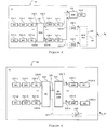
- FIG. 1 illustrates the block diagram of an exemplary embodiment of a first photonic integrated circuit 10, which can be provided in a single substrate 11, preferably.
- the laser cavity is essentially composed by a variety of three elements, besides the required reflectors 111-1, 111-m; 111A-1, 111A-n. These elements are: N amplifiers 116-1, 116-n, being N the number of channels, M band-pass filters 112-1, 112-m, being M the number of desired operating bands, and a de-multiplexer 115 1xN. Furthermore, the mentioned reflectors 111-1, 111-m; 111A-1, 111A-n can be replaced by a reflective surface.
- the band-pass filter 112-1, 112-m is tuned to a different operating band and connected to the de-multiplexer 115 through the power combiner 114 and the optical path 121.
- a specific operating band is selected by enabling the corresponding, herein called, band-selector 113-1, 113-m, and disabling the remaining ones.
- These band-selectors can be implemented by an amplifier and the enabling operation corresponds to drive the amplifier, in this case. Note that this is an exemplary embodiment for the said band-selector.
- This invention does not only comprise this solution but also all that use a mechanism, which prohibits the light to pass through an undesirable band-pass filter 112-1, 112-m, such as any other optical/electro-optical switch.
- the de-multiplexer 115 separates each wavelength ⁇ 1 , ⁇ n within the selected band, that reaches the de-multiplexer 115 input through the optical path 121, and provides each of them at the corresponding de-multiplexer 115 output, following the paths 122-1, 122-n. Due to the reflectors at the beginning of the path 120-1, 120-m, and at the end of the path 122-1, 122-n, these paths are bidirectional. A portion of the resulting light of the amplifier 116-1, 116-n driving reaches the reflector 111A-1, 111A-n, where it is reflected back to the amplifier 116,116-n.
- the signal is amplified and follows the optical path 121-120 in direction to reflector 111-1, 111-m.
- the signal is reflected back in direction to the amplifier 116-1, 116-n, being amplified and transmitted to reflector 111A-1, 111A-n, once again.
- the portion of the signal which reaches the power splitter 1x2 117-1, 117-n and is not forwarded to the reflector 111A-1, 111A-n, follows the optical path 123-1, 123-n, i.e., the laser output.
- the constant amplifications and reflections, together with the filtering and de-multiplexing, will provide the channel ⁇ 1 , ⁇ n at the optical path 123-1, 123-n.
- the photonic integrated circuit 10 comprises one amplifier 116-1, 116-n for each channel, the power of each one can be independently adjusted. This way, the channel, which may suffer a power decrease, e.g. due to filtering imperfections, can be amplified without affecting adjacent channels.
- the photonic integrated circuit 10 is only an exemplary embodiment. Any change of this fundamental circuit is also covered, such as, the introduction of additional amplifiers/other elements or the elements location rearrangement.
- FIG.2 illustrates the block diagram of an exemplary embodiment of a second photonic integrated circuit 20, which can be provided in a single substrate 21, preferably.
- photonic integrated circuit 20 is composed by two distinct sub-circuits, each of them can be provide in two substrates, for example.
- One of the mentioned sub-circuits is the first photonic integrated circuit 10 with a slight difference.
- photodiodes for laser monitoring were added.
- the portion of the light that reaches the power splitter 1x2 117-1, 117-n, and is not reflected in reflectors 111A-1, 111A-n will be routed to a second power splitter 1x2 117A-1, 117A-n.
- the photodiode 210-1, 210-n which is connected to one of the power splitter 1x2 117A-1,117A-n outputs, will allow sampling the generated tunable laser signal.
- the resulting electrical signal 310-1,310-n can be used as an input signal of a control unit 211.
- the electrical signal 310-1,310-n will allow verifying if the tunable laser output signal meets the expectations. If it does not, the control unit 211 will change the driving signals 220-1,220-n of the amplifiers 116-1,116-n accordingly.
- power splitter 1x2 117-1,117-n and the power splitter 1x2 117A-1, 117A-n are not necessarily equal.
- the splitting ration of both power splitters has not to be the same.
- power splitter 1x2 117-1,117-n can have a splitting ratio of 50/50, while the power ratio of the power splitter 1x2 117A-1,117A-n can be 10/90. It depends on the portion of the light that is needed to be reflected and the one that is required for the monitoring system, which is composed by the photodiodes and the control unit.
- the other mentioned sub-circuit which is incorporated in photonic integrated circuit 20, relates to the modulation of the tunable laser outputs 123-1,123-n of the photonic integrated circuit 10.
- the modulator 118-1,118-n is connected to the other power splitter 1x2 117A-1,117A-n output.
- the former modulates the signal according to a desired constellation.
- the modulated signal follows the optical path 123A-1,123A-n in direction to the multiplexer Nxl, which multiplexes the N arriving signals into a single one that is transmitted to optical path 124, the output of the tunable transmitter.
- the photodiode 210-1,210-n can be introduced anywhere in the photonic integrated circuit 20. Instead of being introduced at the tunable laser output, the photodiode 210-1,210-n can be placed, e.g., between the amplifier 116-1,116-n and the power splitter 1x2 117-1,117-n.
- the photonic integrated circuit 20 embodiment represented in FIG.2 is an exemplary one. Therefore, it comprises location changes of its elements, as well.
- the photonic integrated circuit 20 comprises one amplifier 116-1,116-n for each channel, the power of each one can be independently adjusted. Also, all channels ⁇ 1 , ⁇ n can convey different information, simultaneously, because they are modulated by independent modulators 118-1,118-n. However, it is also possible to reduce the number of modulators 118-1,118-n if the channels can transmit the same information or if only one amplifier 116-1,116-n is active at a time.
- the reduction of the number of modulators 118-1,118-n implies the introduction of a power combiner Qx1 between the power splitter 1x2 117A-1,117A-n and the mentioned modulator 118-1,118-n, being Q the number of channels that can be modulated by a common modulator 118.
- a power splitter 1xQ has to be introduced, between the modulator 118-1,118-n and the multiplexer Nx1 119, in this case.
- Q N
- all the channels can be modulated with the same information, only one modulator 118 is required a power combiner Nx1 is needed between the power splitter 1x2 117A-1,117A-n and the mentioned modulator 118.
- Q has another value within the interval [0, N]
- the photonic integrated circuit 20 is only an exemplary embodiment. Any change of this circuit is also covered, such as, the introduction of additional amplifiers/other elements or the elements location rearrangement.
- FIG.3 illustrates the block diagram of an exemplary embodiment of a third photonic integrated circuit 30, which can be provided in a single substrate 31, preferably.
- photonic integrated circuit 30 is composed by two distinct sub-circuits, each of them can be provided in a different substrate, for example, as with photonic integrated circuit 20.
- the photonic integrated circuit 30 can be decomposed into the tunable laser cavity and the modulation sub-circuit.
- the former is similar to the photonic integrated circuit 10, except the de-multiplexer 1XN 115 location.
- the de-multiplexer 1xN 115 is located between the power combiner Mxl 114 and the amplifier 116-1,116-n, while in photonic integrated circuit 30, this element (115) is introduced between the power splitter 1x2 117-1,117-n and the reflectors 111A-1,111A-n. Consequently, the power combiner Mxl 114 has to be replaced by a similar element 230 with N outputs, rather than a single one.
- the tunable laser output signals are generated, mainly, due to the constant amplifications and reflections that the light experiences in the amplifier 116-1, 116-n and in the reflectors (or reflective surfaces) 111-1, 111-m, 111A-1,111A-n, respectively.
- the tuning process is dictated by the combination of the band-pass filter 112-1,112-m that has been selected and the de-multiplexer 1xM 115.
- the photodiode 210-1,210-n, together with the control unit 211, is omitted. This omission has only to do with maintaining a good readability of the block diagram.
- the photodiode 210-1,210-n for monitoring, and consequently, the control unit 221, can also be introduced at any point of the photonic integrated circuit 30, as in photonic integrated circuit 20.
- the modulation sub-circuit of photonic integrated circuit 30 does not differ from that of the photonic integrated circuit 20. It is composed by modulators 118-1,118-n and a multiplexer Nx1 119, which multiplexes the channels ⁇ 1 , ⁇ n that travels through the optical paths 123-1 to 123-n into the multi-wavelength transmitter output 124.
- the modulators are connected to one of the power splitter 1x2 117-1,117-n outputs, in case of photodiodes 210-1,210-n are not introduced at the tunable laser cavity output. In this case, the modulators are connected to one of the power splitter 1x2 117A-1,117A-n outputs, as it was illustrated in the case of the photonic integrated circuit 20.
- the photonic integrated circuit 20 comprises one amplifier 116-1,116-n for each channel ⁇ 1 , ⁇ n , the power of each one can be independently adjusted. Also, all channels ⁇ 1 , ⁇ n can convey different information, simultaneously, because they are modulated by independent modulators 118-1,118-n. However, it is also possible to reduce the number of modulators 118-1,118-n if the channels can transmit the same information or if only one amplifier 116-1,116-n is active at a time.
- the reduction of the number of modulators 118-1,118-n implies the introduction of a power combiner Qxl between the power splitter 1x2 117A-1,117A-n and the mentioned modulator 118-1,118-n, being Q the number of channels that can be modulated by a common modulator 118.
- a power splitter 1xQ has to be introduced, between the modulator 118-1,118-n and the multiplexer Nx1 119, in this case.
- Q N
- all the channels can be modulated with the same information, only one modulator 118 is required a power combiner Nx1 is needed between the power splitter 1x2 117A-1,117A-n and the mentioned modulator 118.
- Q has another value within the interval [0, N]
- the photonic integrated circuit 30 is only an exemplary embodiment. Any change of this circuit is also covered, such as, the introduction of additional amplifiers/other elements or the elements location rearrangement.
- FIG.4 illustrates the block diagram of an exemplary embodiment of a fourth photonic integrated circuit 40, which can be provided in a single substrate 41, preferably.
- photonic integrated circuit 40 is composed by two distinct sub-circuits, each of them can be provided in a different substrate, for example, as with photonic integrated circuit 20.
- the photonic integrated circuit 40 can be decomposed into the tunable laser cavity and the modulation sub-circuit.
- the former is similar to the photonic integrated circuit 10, except the number and location of the laser cavity outputs 123-1,123-n.
- the laser cavity output is only one, rather than N, as in the photonic integrated circuit 10. The number was reduced due to the localization change.
- the optical path 123-1,123-n is an extension of one of the power splitter 1x2 117-1,117-n output, while in photonic integrated circuit 40, the optical path 123 is located between the de-multiplexer 1xN 115 and the power combiner 114, which has to be replace by a similar element 240, in photonic integrated circuit 40, with the same number of inputs but with two outputs.
- the tunable laser output signal is generated, mainly, due to the constant amplifications and reflections that the light experiences in the amplifier 116-1, 116-n and in the reflectors (or reflective surfaces) 111-1,111-m, 111A-1, 111A-n, respectively.
- the tuning process is dictated by the combination of the band-pass filter 112-1,112-m that has been selected and the de-multiplexer 1xM 115.
- the photodiode 210-1,210-n, together with the control unit 211, is omitted. This omission has only to do with maintaining a good readability of the block diagram.
- the photodiode 210-1,210-n for monitoring, and consequently, the control unit 221, can also be introduced at any point of the photonic integrated circuit 40, as in photonic integrated circuit 20.
- the modulation sub-circuit of photonic integrated circuit 40 is composed by only one modulator 118, since there is only one output laser cavity. Thus, if all the gain regions 116-1,116-n are driven simultaneously, all channels ⁇ 1 , ⁇ n will convey the same information.
- the photonic integrated circuit 40 comprises one amplifier 116-1,116-n for each channel ⁇ 1 , ⁇ n , the power of each one can be independently adjusted.
- the photonic integrated circuit 40 is only an exemplary embodiment. Any change of this circuit is also covered, such as, the introduction of additional amplifiers/other elements or the elements location rearrangement.
Landscapes
- Physics & Mathematics (AREA)
- Electromagnetism (AREA)
- Optics & Photonics (AREA)
- Engineering & Computer Science (AREA)
- Plasma & Fusion (AREA)
- Condensed Matter Physics & Semiconductors (AREA)
- General Physics & Mathematics (AREA)
- Computer Networks & Wireless Communication (AREA)
- Signal Processing (AREA)
- Automation & Control Theory (AREA)
- Semiconductor Lasers (AREA)
- Optical Integrated Circuits (AREA)
- Optical Modulation, Optical Deflection, Nonlinear Optics, Optical Demodulation, Optical Logic Elements (AREA)
- Optical Communication System (AREA)
Claims (14)
- Un circuit intégré photonique (10) comprenant :Un substrat (11) ;Une cavité laser prévue dans le substrat (11) comprenant :une pluralité de premiers réflecteurs (111-1, 111-m) et deuxièmes réflecteurs (111A-1, 111A-n), disposés aux deux extrémités de ladite cavité laser ;une pluralité de filtres passe-bande (112-1, 112-m), chacun relié à chacun des premiers réflecteurs (111-1, 111-m), configurés pour fonctionner chacun dans une certaine bande ;une pluralité de sélecteurs de bande (113-1, 113-m), chacun relié à chacun desdits filtres passe-bande (112-1, 112-m), qui sert à activer ou désactiver la bande respective ;un combineur de puissance (114) relié à la sortie de chaque sélecteur de bande (113-1, 113-m), qui agrège toutes les entités susmentionnées dans un seul trajet optique (121) ;un filtre multibande (115), avec une entrée où est reliée la sortie dudit combineur de puissance (114), et de multiples sorties ;une multiplicité d'amplificateurs (116-1, 116-n), chacun relié à une sortie dudit filtre multibande (115) ;une multiplicité de diviseurs de puissance (117-l, 117-n), où l'entrée de chacun d'eux est reliée à chaque amplificateur (116-1, 116-n), et ayant deux sorties chacun, où la première sortie d'un diviseur de puissance est reliée à un deuxième réflecteur (111A-1, 111A-n) ;une pluralité de sorties, chacune formée par la deuxième sortie d'un diviseur de puissance qui n'est pas reliée au deuxième réflecteur (111A-1, 111A-n).
- Le circuit intégré photonique (10) de la revendication 1, où• chacun de la pluralité de premiers et deuxièmes réflecteurs (111-1, 111-m, 111A-1, 111A-n) comprend un réflecteur interféromètre multimode (MIR) ou une surface optiquement réfléchissante, ou• chacune de la pluralité de filtres passe-bande (112-1, 112-m) comprend un réseau sélectif planaire (AWG) ou un réseau de Bragg ou un résonateur en anneau, ou• chaque sélecteur de bande (113-1, 113-m) comprend un commutateur optique ou un amplificateur optique semi-conducteur (SOA) ou un amplificateur dopé à l'erbium, ou• le filtre multibande (115) comprend un réseau sélectif planaire (AWG), ou• chaque amplificateur (116-1, 116-n) comprend un amplificateur optique semi-conducteur (SOA) ou un amplificateur dopé à l'erbium, ou• le combineur de puissance (114) comprend un interféromètre multimode (MMI) ou chaque diviseur de puissance (117-1, 117-n) comprend un interféromètre multimode (MMI).
- Le circuit intégré photonique (20) de la revendication 1, comprenant en outre :
une multiplicité de modulateurs (118-1, 118-n) prévus dans le substrat (21), reliés à la deuxième sortie de chaque diviseur de puissance (117-1, 117-n) et, de préférence :• comprenant également un multiplexeur (119) prévu dans le substrat (21), avec de multiples entrées, où sont reliées les sorties des modulateurs (118-1, 118-n), et avec une sortie, qui est la sortie du circuit (20), ou• chaque modulateur comprend un modulateur de Mach-Zehnder. - Le circuit intégré photonique (20) selon la revendication 3, comprenant en outre :une pluralité de photodétecteurs (210-1, 210-n) prévus dans le substrat (21), chaque photodétecteur comprenant, de préférence, une photodiode PIN ou une photodiode à avalanche (APD) ;une unité de commande électronique (211), ayant comme entrées des signaux électriques (310-1, 310-n) résultant des photodétecteurs (210-1, 210-n) ; ladite unité (211) étant configurée pour :i. traiter lesdits signaux (310-1, 310-n) afin de surveiller le signal optique transmis aux modulateurs (118-1, 118-n) ;ii. agir sur les signaux de commande (220-1, 220-n) des amplificateurs (116-1, 116-n).
- Un circuit intégré photonique (20) selon la revendication 4, comprenant en outre :une multiplicité de diviseurs de puissance (117A-1, 117A-n) prévus dans le substrat (21), ayant une entrée et deux sorties, où l'entrée de chacun d'eux est reliée à la deuxième sortie de chaque diviseur de puissance (117-1, 117-n) qui n'est pas reliée au deuxième réflecteur (111A-1, 111A-n) ; où,une première sortie de chaque diviseur de puissance (117A-1, 117A-n) est reliée au photodétecteur (210-1, 210-n) ;une deuxième sortie de chaque diviseur de puissance (117A-1, 117A-n) est reliée au modulateur (118-1, 118-n).
- Un circuit intégré photonique (30) comprenant :Un substrat (31) ;Une cavité laser prévue dans le substrat (31) comprenant :une pluralité de premiers réflecteurs (111-1, 111-m) et deuxièmes réflecteurs (111A-1, 111A-n), disposés aux deux extrémités de ladite cavité laser ;une pluralité de filtres passe-bande (112-1, 112-m), chacun relié à chacun des premiers réflecteurs (111-1, 111-m), configurés pour fonctionner chacun dans une certaine bande ;une pluralité de sélecteurs de bande (113-1, 113-m), chacun relié à chacun desdits filtres passe-bande (112-1, 112-m), qui sert à activer ou désactiver la bande respective ;un élément (230) ayant de multiples entrées où sont reliées les sorties de chaque sélecteur de bande (113-113-m), et de multiples sorties, étant configuré de manière à entraîner le signal qui circule à travers n'importe quel trajet optique (120-1, 120-m) pour atteindre un amplificateur d'une multiplicité d'amplificateurs (116-1, 116-n).une multiplicité d'amplificateurs (116-1, 116-n), chacun relié à l'une des sorties de l'élément (230) ;une multiplicité de diviseurs de puissance (117-1, 117-n), où l'entrée de chacun d'eux est reliée à chaque amplificateur (116-1, 116-n), et ayant deux sorties chacun ;un filtre multibande (115), avec de multiples entrées où est reliée l'une des sorties des diviseurs de puissance (117-1, 117-n), et avec de multiples sorties où sont reliés les deuxièmes réflecteurs (111A-1, 111A-n) ;une pluralité de sorties, chacune formée par la deuxième sortie d'un diviseur de puissance, ladite deuxième sortie étant celle qui n'est pas reliée au deuxième réflecteur (111A-1, 111A-n) par le filtre multibande (115).
- Le circuit intégré photonique (30) de la revendication 6, où :• chacun de la pluralité de premiers et deuxièmes réflecteurs (111-1, 111-m, 111A-1, 111A-n) comprend un réflecteur interféromètre multimode (MIR) ou une surface optiquement réfléchissante, ou• chacune de la pluralité de filtres passe-bande (112-1, 112-m) comprend un réseau sélectif planaire (AWG) ou un réseau de Bragg ou un résonateur en anneau, ou• chacune de la pluralité de sélecteurs de bande (113-1, 113-m) comprend un commutateur optique ou un amplificateur optique semi-conducteur (SOA) ou un amplificateur dopé à l'erbium, ou• chaque amplificateur (116-1, 116-n) comprend un amplificateur optique semi-conducteur (SOA) ou un amplificateur dopé à l'erbium, ou• le filtre multibande (115) comprend un réseau sélectif planaire (AWG), ou• chaque diviseur de puissance (117-1, 117-n) comprend un interféromètre multimode (MMI), ou chaque élément (230) comprend un interféromètre multimode (MMI).
- Le circuit intégré photonique (30) de la revendication 6, comprenant en outre :
une multiplicité de modulateurs (118-1, 118-n) prévus dans le substrat (31), reliés à la deuxième sortie de chaque diviseur de puissance (117-1, 117-n) et, de préférence :• comprenant également un multiplexeur (119) prévu dans le substrat (31), avec de multiples entrées, où sont reliées les sorties des modulateurs (118-1, 118-n), et avec une sortie, qui est la sortie du circuit (30), ou• chaque modulateur comprend un modulateur de Mach-Zehnder. - Le circuit intégré photonique (30) selon la revendication 8, comprenant en outre :une pluralité de photodétecteurs prévus dans le substrat (31), chaque photodétecteur comprenant, de préférence, une photodiode PIN ou une photodiode à avalanche (APD) ;une unité de commande électronique, ayant comme entrées des signaux électriques résultant des photodétecteurs ; ladite unité de commande étant configurée pour :i. traiter lesdits signaux électriques afin de surveiller le signal optique transmis aux modulateurs (118-1, 118-n) ;ii. agir sur les signaux de commande des amplificateurs (116-1, 116-n).
- Un circuit intégré photonique (30) selon la revendication 9, comprenant en outre :une multiplicité de diviseurs de puissance supplémentaires prévus dans le substrat (31), ayant une entrée et deux sorties, où l'entrée de chacun d'eux est reliée à la deuxième sortie de chaque diviseur de puissance (117-1, 117-n) qui n'est pas reliée au deuxième réflecteur (111A-1, 111A-n) à travers le filtre multibande (115) ; où,une première sortie de chaque diviseur de puissance supplémentaire est reliée au photodétecteur ;une deuxième sortie de chaque diviseur de puissance supplémentaire est reliée au modulateur (118-1, 118-n).
- Un circuit intégré photonique (40) comprenant :Un substrat (41) ;Une cavité laser prévue dans le substrat (41) comprenant :une pluralité de premiers réflecteurs (111-1, 111-m) et deuxièmes réflecteurs (111A-1, 111A-n), disposés aux deux extrémités de ladite cavité laser ;une pluralité de filtres passe-bande (112-1, 112-m), chacun relié à chacun des premiers réflecteurs (111-1, 111-m), configurés pour fonctionner chacun dans une certaine bande ;une pluralité de sélecteurs de bande (113-1, 113-m), chacun relié à chacun desdits filtres passe-bande (112-1, 112-m) ;un combineur de puissance (114), avec de multiples entrées reliant la sortie de chaque sélecteur de bande (113-1, 113-m) et avec deux sorties ;un filtre multibande (115), avec une entrée où est reliée une première sortie du combineur de puissance (114), et avec de multiples sorties ;une multiplicité d'amplificateurs (116-1, 116-n), chacun relié à l'une des sorties du filtre multibande (115) ; la sortie de chaque amplificateur (116-1, 116-n) étant reliée aux deuxièmes réflecteurs (111A-1, 111A-n) ;une sortie, formée par une deuxième sortie du combineur de puissance (114), ladite deuxième sortie étant celle qui n'est pas reliée au filtre multibande (115).
- Le circuit intégré photonique (40) de la revendication 11, où :• chacun de la pluralité de premiers et deuxièmes réflecteurs (111-1, 111-m, 111A-1, 111A-n) comprend un réflecteur interféromètre multimode (MIR) ou une surface optiquement réfléchissante, ou• chacun de la pluralité de filtres passe-bande (112-1, 112-m) comprend un réseau sélectif planaire (AWG) ou un réseau de Bragg ou un résonateur en anneau, ou• chacun de la pluralité de sélecteurs de bande (113-1, 113-m) comprend un commutateur optique ou un amplificateur optique semi-conducteur (SOA) ou un amplificateur dopé à l'erbium, ou• le filtre multibande (115) comprend un réseau sélectif planaire (AWG), ou• chaque amplificateur (116-1, 116-n) comprend un amplificateur optique semi-conducteur (SOA) ou un amplificateur dopé à l'erbium, ou• le combineur de puissance (114) comprend un interféromètre multimode (MMI).
- Le circuit intégré photonique (40) de la revendication 11, comprenant en outre un modulateur (118) prévu dans le substrat (41), relié à la deuxième sortie du combineur de puissance (114) ; la sortie du modulateur (118) étant la sortie du circuit (40) et, de préférence, le modulateur (118) comprend un modulateur de Mach-Zehnder.
- Le circuit intégré photonique (40) selon la revendication 13, comprenant en outre :une pluralité de photodétecteurs prévus dans le substrat (41), chaque photodétecteur comprenant, de préférence, une photodiode PIN ou une photodiode à avalanche (APD) ;une unité de commande électronique, ayant comme entrées des signaux électriques résultant des photodétecteurs ; ladite unité de commande étant configurée pour :i. traiter lesdits signaux électriques afin de surveiller le signal optique transmis au modulateur (118) ;ii. agir sur les signaux de commande des amplificateurs (116-1, 116-n).
Applications Claiming Priority (2)
| Application Number | Priority Date | Filing Date | Title |
|---|---|---|---|
| PT107719A PT107719A (pt) | 2014-06-19 | 2014-06-19 | Circuito integrado óptico transmissor sintonizável de múltiplos comprimentos de onda |
| PCT/PT2015/000029 WO2015194982A1 (fr) | 2014-06-19 | 2015-06-18 | Circuit émetteur à longueurs d'onde multiples, photonique, accordable, intégré |
Publications (2)
| Publication Number | Publication Date |
|---|---|
| EP3158666A1 EP3158666A1 (fr) | 2017-04-26 |
| EP3158666B1 true EP3158666B1 (fr) | 2019-07-31 |
Family
ID=53610961
Family Applications (1)
| Application Number | Title | Priority Date | Filing Date |
|---|---|---|---|
| EP15738492.6A Active EP3158666B1 (fr) | 2014-06-19 | 2015-06-18 | Circuit émetteur à longueurs d'onde multiples, photonique, accordable, intégré |
Country Status (5)
| Country | Link |
|---|---|
| US (1) | US10326529B2 (fr) |
| EP (1) | EP3158666B1 (fr) |
| ES (1) | ES2751632T3 (fr) |
| PT (2) | PT107719A (fr) |
| WO (1) | WO2015194982A1 (fr) |
Families Citing this family (1)
| Publication number | Priority date | Publication date | Assignee | Title |
|---|---|---|---|---|
| US20250192912A1 (en) * | 2023-12-07 | 2025-06-12 | Lightmatter, Inc. | Wavelength remapping in an on-chip wavelength division multiplexing (wdm) solution |
Family Cites Families (11)
| Publication number | Priority date | Publication date | Assignee | Title |
|---|---|---|---|---|
| US5612968A (en) * | 1995-04-20 | 1997-03-18 | Bell Communications Research, Inc. | Redundant multi-wavelength laser arrays |
| WO2004034530A1 (fr) * | 2002-10-08 | 2004-04-22 | Infinera Corporation | Puces a circuit photonique integre de transmission (txpic) |
| US7020168B2 (en) * | 2003-07-01 | 2006-03-28 | Lucent Technologies Inc. | High power multi-frequency laser |
| US7636522B2 (en) * | 2004-04-15 | 2009-12-22 | Infinera Corporation | Coolerless photonic integrated circuits (PICs) for WDM transmission networks and PICs operable with a floating signal channel grid changing with temperature but with fixed channel spacing in the floating grid |
| US7565084B1 (en) * | 2004-09-15 | 2009-07-21 | Wach Michael L | Robustly stabilizing laser systems |
| JP4973399B2 (ja) * | 2007-09-05 | 2012-07-11 | 日本電気株式会社 | 波長可変光源、その制御方法及び制御プログラム、並びに光モジュール |
| US8643943B2 (en) * | 2008-04-30 | 2014-02-04 | Nec Corporation | Tunable laser source using intracavity laser light outcoupling and module containing the same |
| US9054493B2 (en) * | 2010-06-22 | 2015-06-09 | Oracle International Corporation | Multiple-wavelength laser |
| KR20120070836A (ko) | 2010-12-22 | 2012-07-02 | 한국전자통신연구원 | 다파장 광 발생 장치 |
| US9025241B2 (en) * | 2011-10-14 | 2015-05-05 | Kotura, Inc. | Gain medium providing laser and amplifier functionality to optical device |
| WO2014021781A1 (fr) * | 2012-07-31 | 2014-02-06 | Agency For Science, Technology And Research | Source de lumière optique et émetteur optique |
-
2014
- 2014-06-19 PT PT107719A patent/PT107719A/pt unknown
-
2015
- 2015-06-18 ES ES15738492T patent/ES2751632T3/es active Active
- 2015-06-18 WO PCT/PT2015/000029 patent/WO2015194982A1/fr not_active Ceased
- 2015-06-18 PT PT157384926T patent/PT3158666T/pt unknown
- 2015-06-18 EP EP15738492.6A patent/EP3158666B1/fr active Active
- 2015-06-18 US US15/320,259 patent/US10326529B2/en active Active
Non-Patent Citations (1)
| Title |
|---|
| None * |
Also Published As
| Publication number | Publication date |
|---|---|
| PT107719A (pt) | 2015-12-21 |
| ES2751632T3 (es) | 2020-04-01 |
| EP3158666A1 (fr) | 2017-04-26 |
| WO2015194982A1 (fr) | 2015-12-23 |
| US10326529B2 (en) | 2019-06-18 |
| PT3158666T (pt) | 2019-10-29 |
| US20170331558A1 (en) | 2017-11-16 |
Similar Documents
| Publication | Publication Date | Title |
|---|---|---|
| US7706688B2 (en) | Wavelength reconfigurable optical network | |
| CN107636988B (zh) | 具有改进的光放大的、基于wdm梳状源的光链路 | |
| US7680416B2 (en) | WDM-PON having optical source of self-injection locked fabry-perot laser diode | |
| JP3978168B2 (ja) | 中央局から生成された多波長光のループバックを利用する受動型光通信網 | |
| EP3487091B1 (fr) | Procédé et système permettant d'établir au moins deux liaisons de communication bidirectionnelles au moyen d'une détection cohérente | |
| Welch et al. | The realization of large-scale photonic integrated circuits and the associated impact on fiber-optic communication systems | |
| JP2005536078A (ja) | 波長ロックされた波長分割多重化光源に基づく波長分割多重パッシーブ光ネットワークを提供する方法および装置 | |
| WO2012065460A1 (fr) | Procédé et système de réseau optique passif, terminal de ligne optique et unité de routage de longueur d'onde | |
| US20130058650A1 (en) | Method and system for flexible optical signal aggregation and transmission | |
| US9020358B2 (en) | Wavelength division multiplexing transmission equipment | |
| US12526055B2 (en) | Photonic integrated circuit for high-wavelength-channel-count wavelength-division-multiplexed systems | |
| KR101367486B1 (ko) | 파장 분할 다중 액세스 네트워크를 운용하는 장치 및 방법 | |
| EP1356620B1 (fr) | Systeme de communication optique a mrl | |
| US10761263B1 (en) | Multi-channel, densely-spaced wavelength division multiplexing transceiver | |
| KR100605925B1 (ko) | 파장분할다중 방식의 수동형 광 가입자망 | |
| CN104767584B (zh) | 一种用于twdm-pon系统的光网络单元的反射光调制器 | |
| EP3158666B1 (fr) | Circuit émetteur à longueurs d'onde multiples, photonique, accordable, intégré | |
| JP4230934B2 (ja) | 多チャンネル光変調装置および多チャンネル光送信装置 | |
| CN102725981B (zh) | 波分复用/解复用器、自注入光纤激光器和光网络系统 | |
| EP2613461B1 (fr) | Transmetteur optique pour réseau optique WDM | |
| CA2593891C (fr) | Reseau optique a longueur d'onde reconfigurable | |
| Raz et al. | Optically reconfigurable 1× 4 silicon-on-insulator remote node switch for access networks | |
| EP2894800B1 (fr) | Procédé et dispositif d'interconnexion optique | |
| JP2014204420A (ja) | 光波長分割多重伝送システム | |
| WO2021100070A1 (fr) | Modulateur optique et émetteur optique |
Legal Events
| Date | Code | Title | Description |
|---|---|---|---|
| STAA | Information on the status of an ep patent application or granted ep patent |
Free format text: STATUS: THE INTERNATIONAL PUBLICATION HAS BEEN MADE |
|
| PUAI | Public reference made under article 153(3) epc to a published international application that has entered the european phase |
Free format text: ORIGINAL CODE: 0009012 |
|
| STAA | Information on the status of an ep patent application or granted ep patent |
Free format text: STATUS: REQUEST FOR EXAMINATION WAS MADE |
|
| 17P | Request for examination filed |
Effective date: 20170118 |
|
| AK | Designated contracting states |
Kind code of ref document: A1 Designated state(s): AL AT BE BG CH CY CZ DE DK EE ES FI FR GB GR HR HU IE IS IT LI LT LU LV MC MK MT NL NO PL PT RO RS SE SI SK SM TR |
|
| AX | Request for extension of the european patent |
Extension state: BA ME |
|
| DAV | Request for validation of the european patent (deleted) | ||
| DAX | Request for extension of the european patent (deleted) | ||
| STAA | Information on the status of an ep patent application or granted ep patent |
Free format text: STATUS: EXAMINATION IS IN PROGRESS |
|
| 17Q | First examination report despatched |
Effective date: 20180517 |
|
| GRAP | Despatch of communication of intention to grant a patent |
Free format text: ORIGINAL CODE: EPIDOSNIGR1 |
|
| STAA | Information on the status of an ep patent application or granted ep patent |
Free format text: STATUS: GRANT OF PATENT IS INTENDED |
|
| INTG | Intention to grant announced |
Effective date: 20190318 |
|
| GRAS | Grant fee paid |
Free format text: ORIGINAL CODE: EPIDOSNIGR3 |
|
| GRAA | (expected) grant |
Free format text: ORIGINAL CODE: 0009210 |
|
| STAA | Information on the status of an ep patent application or granted ep patent |
Free format text: STATUS: THE PATENT HAS BEEN GRANTED |
|
| AK | Designated contracting states |
Kind code of ref document: B1 Designated state(s): AL AT BE BG CH CY CZ DE DK EE ES FI FR GB GR HR HU IE IS IT LI LT LU LV MC MK MT NL NO PL PT RO RS SE SI SK SM TR |
|
| REG | Reference to a national code |
Ref country code: CH Ref legal event code: EP Ref country code: GB Ref legal event code: FG4D |
|
| REG | Reference to a national code |
Ref country code: AT Ref legal event code: REF Ref document number: 1162079 Country of ref document: AT Kind code of ref document: T Effective date: 20190815 |
|
| REG | Reference to a national code |
Ref country code: IE Ref legal event code: FG4D |
|
| REG | Reference to a national code |
Ref country code: DE Ref legal event code: R096 Ref document number: 602015034807 Country of ref document: DE |
|
| REG | Reference to a national code |
Ref country code: PT Ref legal event code: SC4A Ref document number: 3158666 Country of ref document: PT Date of ref document: 20191029 Kind code of ref document: T Free format text: AVAILABILITY OF NATIONAL TRANSLATION Effective date: 20191014 |
|
| REG | Reference to a national code |
Ref country code: NL Ref legal event code: MP Effective date: 20190731 |
|
| REG | Reference to a national code |
Ref country code: LT Ref legal event code: MG4D |
|
| REG | Reference to a national code |
Ref country code: AT Ref legal event code: MK05 Ref document number: 1162079 Country of ref document: AT Kind code of ref document: T Effective date: 20190731 |
|
| PG25 | Lapsed in a contracting state [announced via postgrant information from national office to epo] |
Ref country code: HR Free format text: LAPSE BECAUSE OF FAILURE TO SUBMIT A TRANSLATION OF THE DESCRIPTION OR TO PAY THE FEE WITHIN THE PRESCRIBED TIME-LIMIT Effective date: 20190731 Ref country code: LT Free format text: LAPSE BECAUSE OF FAILURE TO SUBMIT A TRANSLATION OF THE DESCRIPTION OR TO PAY THE FEE WITHIN THE PRESCRIBED TIME-LIMIT Effective date: 20190731 Ref country code: BG Free format text: LAPSE BECAUSE OF FAILURE TO SUBMIT A TRANSLATION OF THE DESCRIPTION OR TO PAY THE FEE WITHIN THE PRESCRIBED TIME-LIMIT Effective date: 20191031 Ref country code: SE Free format text: LAPSE BECAUSE OF FAILURE TO SUBMIT A TRANSLATION OF THE DESCRIPTION OR TO PAY THE FEE WITHIN THE PRESCRIBED TIME-LIMIT Effective date: 20190731 Ref country code: NL Free format text: LAPSE BECAUSE OF FAILURE TO SUBMIT A TRANSLATION OF THE DESCRIPTION OR TO PAY THE FEE WITHIN THE PRESCRIBED TIME-LIMIT Effective date: 20190731 Ref country code: FI Free format text: LAPSE BECAUSE OF FAILURE TO SUBMIT A TRANSLATION OF THE DESCRIPTION OR TO PAY THE FEE WITHIN THE PRESCRIBED TIME-LIMIT Effective date: 20190731 Ref country code: NO Free format text: LAPSE BECAUSE OF FAILURE TO SUBMIT A TRANSLATION OF THE DESCRIPTION OR TO PAY THE FEE WITHIN THE PRESCRIBED TIME-LIMIT Effective date: 20191031 Ref country code: AT Free format text: LAPSE BECAUSE OF FAILURE TO SUBMIT A TRANSLATION OF THE DESCRIPTION OR TO PAY THE FEE WITHIN THE PRESCRIBED TIME-LIMIT Effective date: 20190731 |
|
| PG25 | Lapsed in a contracting state [announced via postgrant information from national office to epo] |
Ref country code: RS Free format text: LAPSE BECAUSE OF FAILURE TO SUBMIT A TRANSLATION OF THE DESCRIPTION OR TO PAY THE FEE WITHIN THE PRESCRIBED TIME-LIMIT Effective date: 20190731 Ref country code: LV Free format text: LAPSE BECAUSE OF FAILURE TO SUBMIT A TRANSLATION OF THE DESCRIPTION OR TO PAY THE FEE WITHIN THE PRESCRIBED TIME-LIMIT Effective date: 20190731 Ref country code: AL Free format text: LAPSE BECAUSE OF FAILURE TO SUBMIT A TRANSLATION OF THE DESCRIPTION OR TO PAY THE FEE WITHIN THE PRESCRIBED TIME-LIMIT Effective date: 20190731 Ref country code: IS Free format text: LAPSE BECAUSE OF FAILURE TO SUBMIT A TRANSLATION OF THE DESCRIPTION OR TO PAY THE FEE WITHIN THE PRESCRIBED TIME-LIMIT Effective date: 20191130 |
|
| PG25 | Lapsed in a contracting state [announced via postgrant information from national office to epo] |
Ref country code: TR Free format text: LAPSE BECAUSE OF FAILURE TO SUBMIT A TRANSLATION OF THE DESCRIPTION OR TO PAY THE FEE WITHIN THE PRESCRIBED TIME-LIMIT Effective date: 20190731 |
|
| REG | Reference to a national code |
Ref country code: ES Ref legal event code: FG2A Ref document number: 2751632 Country of ref document: ES Kind code of ref document: T3 Effective date: 20200401 |
|
| PG25 | Lapsed in a contracting state [announced via postgrant information from national office to epo] |
Ref country code: DK Free format text: LAPSE BECAUSE OF FAILURE TO SUBMIT A TRANSLATION OF THE DESCRIPTION OR TO PAY THE FEE WITHIN THE PRESCRIBED TIME-LIMIT Effective date: 20190731 Ref country code: EE Free format text: LAPSE BECAUSE OF FAILURE TO SUBMIT A TRANSLATION OF THE DESCRIPTION OR TO PAY THE FEE WITHIN THE PRESCRIBED TIME-LIMIT Effective date: 20190731 Ref country code: IT Free format text: LAPSE BECAUSE OF FAILURE TO SUBMIT A TRANSLATION OF THE DESCRIPTION OR TO PAY THE FEE WITHIN THE PRESCRIBED TIME-LIMIT Effective date: 20190731 Ref country code: RO Free format text: LAPSE BECAUSE OF FAILURE TO SUBMIT A TRANSLATION OF THE DESCRIPTION OR TO PAY THE FEE WITHIN THE PRESCRIBED TIME-LIMIT Effective date: 20190731 Ref country code: PL Free format text: LAPSE BECAUSE OF FAILURE TO SUBMIT A TRANSLATION OF THE DESCRIPTION OR TO PAY THE FEE WITHIN THE PRESCRIBED TIME-LIMIT Effective date: 20190731 |
|
| PG25 | Lapsed in a contracting state [announced via postgrant information from national office to epo] |
Ref country code: SM Free format text: LAPSE BECAUSE OF FAILURE TO SUBMIT A TRANSLATION OF THE DESCRIPTION OR TO PAY THE FEE WITHIN THE PRESCRIBED TIME-LIMIT Effective date: 20190731 Ref country code: IS Free format text: LAPSE BECAUSE OF FAILURE TO SUBMIT A TRANSLATION OF THE DESCRIPTION OR TO PAY THE FEE WITHIN THE PRESCRIBED TIME-LIMIT Effective date: 20200224 Ref country code: SK Free format text: LAPSE BECAUSE OF FAILURE TO SUBMIT A TRANSLATION OF THE DESCRIPTION OR TO PAY THE FEE WITHIN THE PRESCRIBED TIME-LIMIT Effective date: 20190731 Ref country code: CZ Free format text: LAPSE BECAUSE OF FAILURE TO SUBMIT A TRANSLATION OF THE DESCRIPTION OR TO PAY THE FEE WITHIN THE PRESCRIBED TIME-LIMIT Effective date: 20190731 |
|
| REG | Reference to a national code |
Ref country code: DE Ref legal event code: R097 Ref document number: 602015034807 Country of ref document: DE |
|
| PLBE | No opposition filed within time limit |
Free format text: ORIGINAL CODE: 0009261 |
|
| STAA | Information on the status of an ep patent application or granted ep patent |
Free format text: STATUS: NO OPPOSITION FILED WITHIN TIME LIMIT |
|
| PG2D | Information on lapse in contracting state deleted |
Ref country code: IS |
|
| PG25 | Lapsed in a contracting state [announced via postgrant information from national office to epo] |
Ref country code: IS Free format text: LAPSE BECAUSE OF FAILURE TO SUBMIT A TRANSLATION OF THE DESCRIPTION OR TO PAY THE FEE WITHIN THE PRESCRIBED TIME-LIMIT Effective date: 20191030 |
|
| 26N | No opposition filed |
Effective date: 20200603 |
|
| PG25 | Lapsed in a contracting state [announced via postgrant information from national office to epo] |
Ref country code: SI Free format text: LAPSE BECAUSE OF FAILURE TO SUBMIT A TRANSLATION OF THE DESCRIPTION OR TO PAY THE FEE WITHIN THE PRESCRIBED TIME-LIMIT Effective date: 20190731 |
|
| PG25 | Lapsed in a contracting state [announced via postgrant information from national office to epo] |
Ref country code: MC Free format text: LAPSE BECAUSE OF FAILURE TO SUBMIT A TRANSLATION OF THE DESCRIPTION OR TO PAY THE FEE WITHIN THE PRESCRIBED TIME-LIMIT Effective date: 20190731 |
|
| REG | Reference to a national code |
Ref country code: CH Ref legal event code: PL |
|
| PG25 | Lapsed in a contracting state [announced via postgrant information from national office to epo] |
Ref country code: LU Free format text: LAPSE BECAUSE OF NON-PAYMENT OF DUE FEES Effective date: 20200618 |
|
| REG | Reference to a national code |
Ref country code: BE Ref legal event code: MM Effective date: 20200630 |
|
| PG25 | Lapsed in a contracting state [announced via postgrant information from national office to epo] |
Ref country code: LI Free format text: LAPSE BECAUSE OF NON-PAYMENT OF DUE FEES Effective date: 20200630 Ref country code: CH Free format text: LAPSE BECAUSE OF NON-PAYMENT OF DUE FEES Effective date: 20200630 Ref country code: IE Free format text: LAPSE BECAUSE OF NON-PAYMENT OF DUE FEES Effective date: 20200618 |
|
| PG25 | Lapsed in a contracting state [announced via postgrant information from national office to epo] |
Ref country code: BE Free format text: LAPSE BECAUSE OF NON-PAYMENT OF DUE FEES Effective date: 20200630 |
|
| PGFP | Annual fee paid to national office [announced via postgrant information from national office to epo] |
Ref country code: DE Payment date: 20210628 Year of fee payment: 7 Ref country code: FR Payment date: 20210629 Year of fee payment: 7 Ref country code: PT Payment date: 20210614 Year of fee payment: 7 |
|
| PGFP | Annual fee paid to national office [announced via postgrant information from national office to epo] |
Ref country code: GB Payment date: 20210615 Year of fee payment: 7 |
|
| PGFP | Annual fee paid to national office [announced via postgrant information from national office to epo] |
Ref country code: ES Payment date: 20210701 Year of fee payment: 7 |
|
| PG25 | Lapsed in a contracting state [announced via postgrant information from national office to epo] |
Ref country code: MT Free format text: LAPSE BECAUSE OF FAILURE TO SUBMIT A TRANSLATION OF THE DESCRIPTION OR TO PAY THE FEE WITHIN THE PRESCRIBED TIME-LIMIT Effective date: 20190731 Ref country code: CY Free format text: LAPSE BECAUSE OF FAILURE TO SUBMIT A TRANSLATION OF THE DESCRIPTION OR TO PAY THE FEE WITHIN THE PRESCRIBED TIME-LIMIT Effective date: 20190731 |
|
| PG25 | Lapsed in a contracting state [announced via postgrant information from national office to epo] |
Ref country code: MK Free format text: LAPSE BECAUSE OF FAILURE TO SUBMIT A TRANSLATION OF THE DESCRIPTION OR TO PAY THE FEE WITHIN THE PRESCRIBED TIME-LIMIT Effective date: 20190731 |
|
| PG25 | Lapsed in a contracting state [announced via postgrant information from national office to epo] |
Ref country code: GR Free format text: LAPSE BECAUSE OF FAILURE TO SUBMIT A TRANSLATION OF THE DESCRIPTION OR TO PAY THE FEE WITHIN THE PRESCRIBED TIME-LIMIT Effective date: 20190731 |
|
| REG | Reference to a national code |
Ref country code: DE Ref legal event code: R119 Ref document number: 602015034807 Country of ref document: DE |
|
| PG25 | Lapsed in a contracting state [announced via postgrant information from national office to epo] |
Ref country code: PT Free format text: LAPSE BECAUSE OF NON-PAYMENT OF DUE FEES Effective date: 20221219 |
|
| GBPC | Gb: european patent ceased through non-payment of renewal fee |
Effective date: 20220618 |
|
| PG25 | Lapsed in a contracting state [announced via postgrant information from national office to epo] |
Ref country code: FR Free format text: LAPSE BECAUSE OF NON-PAYMENT OF DUE FEES Effective date: 20220630 |
|
| PG25 | Lapsed in a contracting state [announced via postgrant information from national office to epo] |
Ref country code: GB Free format text: LAPSE BECAUSE OF NON-PAYMENT OF DUE FEES Effective date: 20220618 Ref country code: DE Free format text: LAPSE BECAUSE OF NON-PAYMENT OF DUE FEES Effective date: 20230103 |
|
| REG | Reference to a national code |
Ref country code: ES Ref legal event code: FD2A Effective date: 20230728 |
|
| PG25 | Lapsed in a contracting state [announced via postgrant information from national office to epo] |
Ref country code: ES Free format text: LAPSE BECAUSE OF NON-PAYMENT OF DUE FEES Effective date: 20220619 |