EP3159155B1 - Cellule solaire sensibilisée par colorant comprenant un substrat composite - Google Patents
Cellule solaire sensibilisée par colorant comprenant un substrat composite Download PDFInfo
- Publication number
- EP3159155B1 EP3159155B1 EP16203369.0A EP16203369A EP3159155B1 EP 3159155 B1 EP3159155 B1 EP 3159155B1 EP 16203369 A EP16203369 A EP 16203369A EP 3159155 B1 EP3159155 B1 EP 3159155B1
- Authority
- EP
- European Patent Office
- Prior art keywords
- woven
- microfibers
- layer
- substrate
- glass
- Prior art date
- Legal status (The legal status is an assumption and is not a legal conclusion. Google has not performed a legal analysis and makes no representation as to the accuracy of the status listed.)
- Active
Links
Images
Classifications
-
- H—ELECTRICITY
- H01—ELECTRIC ELEMENTS
- H01G—CAPACITORS; CAPACITORS, RECTIFIERS, DETECTORS, SWITCHING DEVICES, LIGHT-SENSITIVE OR TEMPERATURE-SENSITIVE DEVICES OF THE ELECTROLYTIC TYPE
- H01G9/00—Electrolytic capacitors, rectifiers, detectors, switching devices, light-sensitive or temperature-sensitive devices; Processes of their manufacture
- H01G9/20—Light-sensitive devices
- H01G9/2068—Panels or arrays of photoelectrochemical cells, e.g. photovoltaic modules based on photoelectrochemical cells
-
- H—ELECTRICITY
- H01—ELECTRIC ELEMENTS
- H01G—CAPACITORS; CAPACITORS, RECTIFIERS, DETECTORS, SWITCHING DEVICES, LIGHT-SENSITIVE OR TEMPERATURE-SENSITIVE DEVICES OF THE ELECTROLYTIC TYPE
- H01G9/00—Electrolytic capacitors, rectifiers, detectors, switching devices, light-sensitive or temperature-sensitive devices; Processes of their manufacture
- H01G9/20—Light-sensitive devices
-
- H—ELECTRICITY
- H10—SEMICONDUCTOR DEVICES; ELECTRIC SOLID-STATE DEVICES NOT OTHERWISE PROVIDED FOR
- H10F—INORGANIC SEMICONDUCTOR DEVICES SENSITIVE TO INFRARED RADIATION, LIGHT, ELECTROMAGNETIC RADIATION OF SHORTER WAVELENGTH OR CORPUSCULAR RADIATION
- H10F10/00—Individual photovoltaic cells, e.g. solar cells
-
- B—PERFORMING OPERATIONS; TRANSPORTING
- B05—SPRAYING OR ATOMISING IN GENERAL; APPLYING FLUENT MATERIALS TO SURFACES, IN GENERAL
- B05D—PROCESSES FOR APPLYING FLUENT MATERIALS TO SURFACES, IN GENERAL
- B05D7/00—Processes, other than flocking, specially adapted for applying liquids or other fluent materials to particular surfaces or for applying particular liquids or other fluent materials
- B05D7/50—Multilayers
- B05D7/52—Two layers
- B05D7/54—No clear coat specified
- B05D7/544—No clear coat specified the first layer is let to dry at least partially before applying the second layer
-
- B—PERFORMING OPERATIONS; TRANSPORTING
- B32—LAYERED PRODUCTS
- B32B—LAYERED PRODUCTS, i.e. PRODUCTS BUILT-UP OF STRATA OF FLAT OR NON-FLAT, e.g. CELLULAR OR HONEYCOMB, FORM
- B32B5/00—Layered products characterised by the non- homogeneity or physical structure, i.e. comprising a fibrous, filamentary, particulate or foam layer; Layered products characterised by having a layer differing constitutionally or physically in different parts
- B32B5/02—Layered products characterised by the non- homogeneity or physical structure, i.e. comprising a fibrous, filamentary, particulate or foam layer; Layered products characterised by having a layer differing constitutionally or physically in different parts characterised by structural features of a fibrous or filamentary layer
- B32B5/022—Non-woven fabric
-
- B—PERFORMING OPERATIONS; TRANSPORTING
- B32—LAYERED PRODUCTS
- B32B—LAYERED PRODUCTS, i.e. PRODUCTS BUILT-UP OF STRATA OF FLAT OR NON-FLAT, e.g. CELLULAR OR HONEYCOMB, FORM
- B32B5/00—Layered products characterised by the non- homogeneity or physical structure, i.e. comprising a fibrous, filamentary, particulate or foam layer; Layered products characterised by having a layer differing constitutionally or physically in different parts
- B32B5/02—Layered products characterised by the non- homogeneity or physical structure, i.e. comprising a fibrous, filamentary, particulate or foam layer; Layered products characterised by having a layer differing constitutionally or physically in different parts characterised by structural features of a fibrous or filamentary layer
- B32B5/024—Woven fabric
-
- B—PERFORMING OPERATIONS; TRANSPORTING
- B32—LAYERED PRODUCTS
- B32B—LAYERED PRODUCTS, i.e. PRODUCTS BUILT-UP OF STRATA OF FLAT OR NON-FLAT, e.g. CELLULAR OR HONEYCOMB, FORM
- B32B5/00—Layered products characterised by the non- homogeneity or physical structure, i.e. comprising a fibrous, filamentary, particulate or foam layer; Layered products characterised by having a layer differing constitutionally or physically in different parts
- B32B5/22—Layered products characterised by the non- homogeneity or physical structure, i.e. comprising a fibrous, filamentary, particulate or foam layer; Layered products characterised by having a layer differing constitutionally or physically in different parts characterised by the presence of two or more layers which are next to each other and are fibrous, filamentary, formed of particles or foamed
- B32B5/24—Layered products characterised by the non- homogeneity or physical structure, i.e. comprising a fibrous, filamentary, particulate or foam layer; Layered products characterised by having a layer differing constitutionally or physically in different parts characterised by the presence of two or more layers which are next to each other and are fibrous, filamentary, formed of particles or foamed one layer being a fibrous or filamentary layer
- B32B5/26—Layered products characterised by the non- homogeneity or physical structure, i.e. comprising a fibrous, filamentary, particulate or foam layer; Layered products characterised by having a layer differing constitutionally or physically in different parts characterised by the presence of two or more layers which are next to each other and are fibrous, filamentary, formed of particles or foamed one layer being a fibrous or filamentary layer another layer next to it also being fibrous or filamentary
-
- H—ELECTRICITY
- H01—ELECTRIC ELEMENTS
- H01G—CAPACITORS; CAPACITORS, RECTIFIERS, DETECTORS, SWITCHING DEVICES, LIGHT-SENSITIVE OR TEMPERATURE-SENSITIVE DEVICES OF THE ELECTROLYTIC TYPE
- H01G9/00—Electrolytic capacitors, rectifiers, detectors, switching devices, light-sensitive or temperature-sensitive devices; Processes of their manufacture
- H01G9/0029—Processes of manufacture
- H01G9/0032—Processes of manufacture formation of the dielectric layer
-
- H—ELECTRICITY
- H01—ELECTRIC ELEMENTS
- H01G—CAPACITORS; CAPACITORS, RECTIFIERS, DETECTORS, SWITCHING DEVICES, LIGHT-SENSITIVE OR TEMPERATURE-SENSITIVE DEVICES OF THE ELECTROLYTIC TYPE
- H01G9/00—Electrolytic capacitors, rectifiers, detectors, switching devices, light-sensitive or temperature-sensitive devices; Processes of their manufacture
- H01G9/20—Light-sensitive devices
- H01G9/2068—Panels or arrays of photoelectrochemical cells, e.g. photovoltaic modules based on photoelectrochemical cells
- H01G9/2081—Serial interconnection of cells
-
- H—ELECTRICITY
- H01—ELECTRIC ELEMENTS
- H01G—CAPACITORS; CAPACITORS, RECTIFIERS, DETECTORS, SWITCHING DEVICES, LIGHT-SENSITIVE OR TEMPERATURE-SENSITIVE DEVICES OF THE ELECTROLYTIC TYPE
- H01G9/00—Electrolytic capacitors, rectifiers, detectors, switching devices, light-sensitive or temperature-sensitive devices; Processes of their manufacture
- H01G9/20—Light-sensitive devices
- H01G9/2095—Light-sensitive devices comprising a flexible sustrate
-
- H—ELECTRICITY
- H10—SEMICONDUCTOR DEVICES; ELECTRIC SOLID-STATE DEVICES NOT OTHERWISE PROVIDED FOR
- H10F—INORGANIC SEMICONDUCTOR DEVICES SENSITIVE TO INFRARED RADIATION, LIGHT, ELECTROMAGNETIC RADIATION OF SHORTER WAVELENGTH OR CORPUSCULAR RADIATION
- H10F77/00—Constructional details of devices covered by this subclass
- H10F77/20—Electrodes
- H10F77/206—Electrodes for devices having potential barriers
- H10F77/211—Electrodes for devices having potential barriers for photovoltaic cells
-
- H—ELECTRICITY
- H10—SEMICONDUCTOR DEVICES; ELECTRIC SOLID-STATE DEVICES NOT OTHERWISE PROVIDED FOR
- H10F—INORGANIC SEMICONDUCTOR DEVICES SENSITIVE TO INFRARED RADIATION, LIGHT, ELECTROMAGNETIC RADIATION OF SHORTER WAVELENGTH OR CORPUSCULAR RADIATION
- H10F99/00—Subject matter not provided for in other groups of this subclass
-
- H—ELECTRICITY
- H10—SEMICONDUCTOR DEVICES; ELECTRIC SOLID-STATE DEVICES NOT OTHERWISE PROVIDED FOR
- H10K—ORGANIC ELECTRIC SOLID-STATE DEVICES
- H10K71/00—Manufacture or treatment specially adapted for the organic devices covered by this subclass
- H10K71/60—Forming conductive regions or layers, e.g. electrodes
- H10K71/611—Forming conductive regions or layers, e.g. electrodes using printing deposition, e.g. ink jet printing
-
- B—PERFORMING OPERATIONS; TRANSPORTING
- B32—LAYERED PRODUCTS
- B32B—LAYERED PRODUCTS, i.e. PRODUCTS BUILT-UP OF STRATA OF FLAT OR NON-FLAT, e.g. CELLULAR OR HONEYCOMB, FORM
- B32B2262/00—Composition or structural features of fibres which form a fibrous or filamentary layer or are present as additives
- B32B2262/10—Inorganic fibres
-
- B—PERFORMING OPERATIONS; TRANSPORTING
- B32—LAYERED PRODUCTS
- B32B—LAYERED PRODUCTS, i.e. PRODUCTS BUILT-UP OF STRATA OF FLAT OR NON-FLAT, e.g. CELLULAR OR HONEYCOMB, FORM
- B32B2457/00—Electrical equipment
- B32B2457/12—Photovoltaic modules
-
- H—ELECTRICITY
- H01—ELECTRIC ELEMENTS
- H01G—CAPACITORS; CAPACITORS, RECTIFIERS, DETECTORS, SWITCHING DEVICES, LIGHT-SENSITIVE OR TEMPERATURE-SENSITIVE DEVICES OF THE ELECTROLYTIC TYPE
- H01G9/00—Electrolytic capacitors, rectifiers, detectors, switching devices, light-sensitive or temperature-sensitive devices; Processes of their manufacture
- H01G9/20—Light-sensitive devices
- H01G9/2027—Light-sensitive devices comprising an oxide semiconductor electrode
- H01G9/2031—Light-sensitive devices comprising an oxide semiconductor electrode comprising titanium oxide, e.g. TiO2
-
- H—ELECTRICITY
- H01—ELECTRIC ELEMENTS
- H01G—CAPACITORS; CAPACITORS, RECTIFIERS, DETECTORS, SWITCHING DEVICES, LIGHT-SENSITIVE OR TEMPERATURE-SENSITIVE DEVICES OF THE ELECTROLYTIC TYPE
- H01G9/00—Electrolytic capacitors, rectifiers, detectors, switching devices, light-sensitive or temperature-sensitive devices; Processes of their manufacture
- H01G9/20—Light-sensitive devices
- H01G9/2059—Light-sensitive devices comprising an organic dye as the active light absorbing material, e.g. adsorbed on an electrode or dissolved in solution
-
- Y—GENERAL TAGGING OF NEW TECHNOLOGICAL DEVELOPMENTS; GENERAL TAGGING OF CROSS-SECTIONAL TECHNOLOGIES SPANNING OVER SEVERAL SECTIONS OF THE IPC; TECHNICAL SUBJECTS COVERED BY FORMER USPC CROSS-REFERENCE ART COLLECTIONS [XRACs] AND DIGESTS
- Y02—TECHNOLOGIES OR APPLICATIONS FOR MITIGATION OR ADAPTATION AGAINST CLIMATE CHANGE
- Y02E—REDUCTION OF GREENHOUSE GAS [GHG] EMISSIONS, RELATED TO ENERGY GENERATION, TRANSMISSION OR DISTRIBUTION
- Y02E10/00—Energy generation through renewable energy sources
- Y02E10/50—Photovoltaic [PV] energy
- Y02E10/542—Dye sensitized solar cells
-
- Y—GENERAL TAGGING OF NEW TECHNOLOGICAL DEVELOPMENTS; GENERAL TAGGING OF CROSS-SECTIONAL TECHNOLOGIES SPANNING OVER SEVERAL SECTIONS OF THE IPC; TECHNICAL SUBJECTS COVERED BY FORMER USPC CROSS-REFERENCE ART COLLECTIONS [XRACs] AND DIGESTS
- Y02—TECHNOLOGIES OR APPLICATIONS FOR MITIGATION OR ADAPTATION AGAINST CLIMATE CHANGE
- Y02E—REDUCTION OF GREENHOUSE GAS [GHG] EMISSIONS, RELATED TO ENERGY GENERATION, TRANSMISSION OR DISTRIBUTION
- Y02E10/00—Energy generation through renewable energy sources
- Y02E10/50—Photovoltaic [PV] energy
- Y02E10/549—Organic PV cells
-
- Y—GENERAL TAGGING OF NEW TECHNOLOGICAL DEVELOPMENTS; GENERAL TAGGING OF CROSS-SECTIONAL TECHNOLOGIES SPANNING OVER SEVERAL SECTIONS OF THE IPC; TECHNICAL SUBJECTS COVERED BY FORMER USPC CROSS-REFERENCE ART COLLECTIONS [XRACs] AND DIGESTS
- Y02—TECHNOLOGIES OR APPLICATIONS FOR MITIGATION OR ADAPTATION AGAINST CLIMATE CHANGE
- Y02P—CLIMATE CHANGE MITIGATION TECHNOLOGIES IN THE PRODUCTION OR PROCESSING OF GOODS
- Y02P70/00—Climate change mitigation technologies in the production process for final industrial or consumer products
- Y02P70/50—Manufacturing or production processes characterised by the final manufactured product
Definitions
- the present invention relates to a porous insulation substrate.
- DSC Dye-sensitized solar cells
- a conventional sandwich type dye-sensitized solar cell has a few ⁇ m thick porous TiO 2 electrode layer deposited onto a transparent conducting substrate.
- the TiO 2 electrode comprises interconnected TiO 2 metal oxide particles dyed by adsorbing dye molecules on the surface of the TiO 2 particles and forming a working electrode.
- the transparent conducting substrate is normally a transparent conducting oxide deposited onto a glass substrate.
- the transparent conducting oxide layer serves the function as a back contact extracting photo-generated electrons from the working electrode.
- the TiO 2 electrode is in contact with an electrolyte and another transparent conducting substrate, i.e. a counter electrode.
- Sunlight is harvested by the dye, producing photo-excited electrons that are injected into the conduction band of the TiO 2 particles and further collected by the conducting substrate.
- I - ions in the redox electrolyte reduce the oxidized dye and transport the generated electron acceptors species to the counter electrode.
- the two conducting substrates are sealed at the edges in order to protect the DSC modules against the surrounding atmosphere, and to prevent the evaporation or leakage of the DSC components inside the cell.
- WO 2011/096154 discloses a sandwich type DCS module including a porous insulation substrate, a working electrode including a porous conducting metal layer formed on top of the porous insulation substrate and creating a back contact, and a porous semiconductor layer containing an adsorbed dye arranged on top of the porous conducting metal layer, a transparent substrate facing the porous semiconductor layer, adapted to face the sun and to transmit the sun light to the porous semiconductor layer.
- the DSC module further includes a counter electrode including a conducting substrate arranged on a side opposite to the porous semiconductor layer of the porous insulation substrate, and at a distance from the porous insulation substrate, thereby forming a space between the porous insulation substrate and the conducting substrate. An electrolyte is filled in the space between the working electrode and the counter electrode.
- the porous conducting metal layer may be created using a paste including metallic or metal based particles, which is applied on top of the porous insulation substrate by printing, and followed by heating, drying and baking.
- An advantage with this type of DSC module is that the conducting layer of the working electrode is arranged between the porous insulation substrate and the porous semiconductor layer.
- the conducting layer of the working cell does not have to be transparent, and can be made of a material of high conductivity, which increases the current-handling capability of the DSC module and ensures high efficiency of the DSC module.
- An ideal porous insulation substrate must fulfill the following requirements: The substrate must have sufficient mechanical strength to withstand the mechanical handling and processing. During the processing of the DSC the substrate is subjected to mechanical handling such as: cutting processes, stacking and de-stacking processes, printing processes, drying processes, air/vacuum sintering processes, sealing processes, etc. Substrates with poor mechanical strength can suffer damage during handling and processing, resulting in defect solar cells, which lower the manufacturing yield.
- the substrate must have sufficient high temperature resistance and exhibit low mechanical deformation and/or small loss in mechanical stability after high temperature treatment.
- the substrate is subjected to temperatures of 500°C in air and (580 - 650)°C in vacuum or inert atmosphere.
- the substrate must withstand temperatures in air up to 500°C without significant mechanical deformation or loss in mechanical stability.
- the substrate must withstand temperatures in vacuum or inert atmosphere of at least up to 580°C or higher without significant mechanical deformation or loss in mechanical stability.
- the substrate must be chemically inert to high temperature processing. During the various high temperature treatments the substrate is exposed to, e.g., hot air, hot air containing organic solvents, hot air containing organic combustion products and to hydrogen gas. The substrate must be chemically inert to all these high temperature treatments and not react chemically to produce compounds that could be harmful for the DSC.
- the substrate must withstand the chemicals used in the DSC.
- the DSC contains active substances such as, e.g., organic solvents, organic dyes, and ions such as I - and I 3- etc.
- active substances such as, e.g., organic solvents, organic dyes, and ions such as I - and I 3- etc.
- the substrate In order to have a good performance stability and life time of the DSC the substrate must not react with the active substances of the DSC to alter the chemical composition of the DSC or produce compounds that could be harmful for the DSC.
- the substrate must allow for fast transport of ions between the electrodes.
- the substrate In order to have fast ion transport between the electrodes, the substrate must have sufficiently high porosity (pore volume fraction) and low tortuosity.
- the substrate has to be electrically insulating. This is to prevent electrical short circuit between the counter electrode and the current collector.
- the distance between the counter electrode and the working electrode is affected by the thickness of the substrate.
- the distance between the counter electrode and the working electrode should be as small as possible such that the transport of ions between the counter electrode and working electrode is as fast as possible. Therefore, the thickness of the substrate should be as thin as possible.
- the substrate must have sufficient capacity to block the conductive particles in the printing ink from seeping through the substrate. In order to avoid electrical short circuit between conducting layers printed on both sides of the substrate, the substrate must be able to block the conductive particles printed on one side of the substrate from seeping through to the other side of the substrate.
- the porous insulation substrate must allow ions to pass through the substrate and prevent particles to pass through the substrate, and must have sufficient mechanical properties.
- a molded fiber glass compact as the porous insulation substrate.
- the molded fiber glass compact can be woven glass fabric containing glass fibers, or non-woven fiberglass in the form of a sheet having glass fibers, which are joined by suitable means.
- the substrate is made of non-woven microglass fibers
- the substrate has to be made very thick in orderto withstand the mechanical handling and processing during manufacturing of the solar cell. This is due to the fact that non-woven glass microfibers have very poor mechanical properties, and accordingly, substrates based on non-woven glass microfibers must be produced with very high thicknesses in order to increase their mechanical stability.
- a substrate with high thickness leads to a large distance between the counter electrode and the working electrode, and accordingly, to a very slow transport of ions between the counter electrode and working electrode.
- Woven glass fibers i.e. glass fabric
- Woven glass fibers include woven yarns of glass microfibers, where each glass fiber yarn consists of multiple glass microfibers.
- Woven glass fibers are inherently mechanically stronger compared to non-woven glass fibers. Additionally, the thickness of woven fibers can be made very thin with maintained mechanical strength. However, woven fibers often have large holes between the woven yarns, which cause a large amount of particles in printed inks to pass right through the substrate in an uncontrolled way across the entire area of the woven fiber causing electrical short circuit between the counter electrode and current collector.
- the holes in the fabric make it difficult to apply an ink including metallic or metal based particles on both sides of the porous insulation substrate without creating an electrical short-circuit, unless the particles are much larger than the holes.
- having such large particles in the ink makes the conducting metal layers too thick. Thick conducting metal layers will increase the distance between the counter electrode and the working electrode resulting in a slower ion transport between the counter electrode and the working electrode.
- US 2006/166582 shows a scrim of woven fiberglass with staple fibres that are needle punched into the woven fiberglass fabric to create a composite structure.
- US 4612237 A discloses an insulating substrate comprising a woven glass scrim, which comprises multifilament yarns, and non-woven fibers disposed on the woven fiberglass scrim.
- the object of the present invention is to provide a porous insulation substrate that fulfills the above-mentioned requirements.
- a microfiber is a fiber having a diameter less than 10 ⁇ m and larger than 1nm.
- a woven fabric can be made very thin and mechanically very strong, but it contains large holes between the woven yarns.
- the non-woven microfiber is mechanically weak, but has excellent filtering properties that blocks conductive particles in the printing ink from seeping through the porous insulation substrate.
- the layer of woven microfibers comprises yarns with holes formed between the individual woven yarns, and at least a part of the non-woven microfibers is accumulated in the holes between the yarns.
- the thickness of the layer of non-woven microfibers varies in dependence of the locations of the holes in the woven layer of microfibers, such that the layer of non-woven microfibers is thicker in the holes in the layer of woven microfibers and thinner on top of the yarns of layer of woven microfibers.
- the layer of non-woven microfibers protrudes into the holes between the yarns. This embodiment reduces the thickness of the layer of non-woven microfibers and makes it possible to provide a thin substrate.
- the porous insulation substrate comprises a second layer of non-woven microfibers arranged on the layer of woven microfibers on a second side of the substrate.
- a second layer of non-woven microfibers on the other side of the layer of woven microfibers, a symmetrical and more mechanically stable substrate is achieved, and the substrate is prevented from curling during the heat treatment during the manufacturing of the solar cell.
- the second layer of non-woven microfibers further enhances the blocking of conductive particles in the inks from passing right through the woven fibers.
- This embodiment provides a smooth surface on both sides of the substrate and thus makes it possible to apply smooth conducting layers on both sides of the substrate by printing.
- the second conducting layer is disposed on the second side of the substrate on the second layer of non-woven microfibers.
- the layer of woven microfibers is made of woven yarns including a plurality of microfibers, in the following denoted filaments, and the diameter of the microfibers in the layer of non-woven microfibers is smaller than the diameter of the filaments in the layer of woven microfibers. This enables the fibers to accumulate in the holes between the yarns and thus block the holes.
- the layer of woven microfibers is made of ceramic microfibers, such as a glass fabric.
- Ceramic microfibers are mechanically very strong and can be made very thin and still be strong enough. Ceramic microfibers can also withstand the high temperatures used in the heat treatment of the solar cell during the manufacturing procedure. Ceramic microfibers are fibers made of a refractory and inert material, such as glass, silica (SiO 2 ), alumina (Al 2 O 3 ), aluminosilicate and quartz.
- the layer of non-woven microfibers is made of ceramic microfibers, such as non-woven glass microfibers.
- the ceramic microfibers can withstand the high temperatures used in the heat treatment of the solar cell during the manufacturing procedure.
- the thickness of the layer of woven microfibers is between 4 ⁇ m and 30 ⁇ m, preferably between 4 ⁇ m and 20 ⁇ m and more preferably between 4 ⁇ m and 10 ⁇ m.
- Such a layer provides the required mechanical strength at the same time as it is thin enough to enable a fast transport of ions between the counter electrode and working electrode.
- the microfibers in the layer of non-woven microfibers have a diameter of less than 4 ⁇ m, preferably less than 1 ⁇ m, and more preferably less than 0.5 ⁇ m.
- the use of very thin fibers reduces the thickness of the layer of non-woven microfibers and accordingly the thickness of the substrate. Further, the thin fibers efficiently block the holes in the layer of woven microfibers and prevent conductive particles from seeping through the substrate and thus prevent the formation of an electrical short circuit.
- the layer of non-woven microfibers comprises organic microfibers.
- Organic microfibers are fibers made of organic materials, such as polymers, for example, polycaprolactone, PET, or PEO, and cellulose, for example nanocellulose (MFC) or wood pulp. It is possible to use organic microfibers in the layer of non-woven microfibers.
- Organic microfibers cannot withstand the high temperatures used in the heat treatment during manufacturing of a dye sensitized solar cell.
- organic microfibers can serve the purpose of blocking the conductive particles in the inks from seeping right through the woven fibers during printing and drying of the inks on the porous insulating substrate, thereby reducing the risk of electrical short circuit.
- the organic microfibers are then removed during heat treatment at higher temperatures. Organic fibers are more flexible and not as fragile as ceramic fibers. Thus, by adding organic fibers, the mechanical strength of substrate increases, which for example is advantageous during a printing and drying process.
- the layer of non-woven microfibers comprises organic microfibers and ceramic microfibers.
- the layer of non-woven microfibers is made of organic and ceramic microfibers.
- An advantage of mixing organic microfibers and ceramic microfibers in the layer of non-woven microfibers is that the organic microfibers are thinner than the ceramic microfibers, thereby creating a nano-network of organic fibers inside a micro network of ceramic fibers and by that reducing the size of the holes in the micro network.
- the organic fibers fill up the holes between the microfibers thereby improving the ability to block the particles in the ink and thus avoiding short circuit.
- the mechanical strength of the substrate is improved compared to only having ceramic microfibers in the substrate.
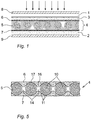
- FIG 1 shows a cross section through a dye-sensitized solar cell (DSC) comprising a porous insulation substrate according to an embodiment of the invention.
- the DSC disclosed in figure 1 is of a monolithic type.
- the DSC comprises a working electrode 1 and a counter electrode 2.
- the space between the working electrode and the counter electrode is filled with an electrolyte including ions for transferring electrons from the counter electrode to the working electrode.
- the DSC module comprises a conducting layer 3 for extracting photo-generated electrons from the working electrode 1.
- the conducting layer 3 serves as a back contact and is in the following named the back contact layer.
- the working electrode 1 includes a porous TiO 2 electrode layer disposed onto the back contact layer 3.
- the TiO 2 electrode comprises TiO 2 particles dyed by adsorbing dye molecules on the surface of the TiO 2 particles.
- the working electrode is positioned on a top side of the DCS module. The top side should be facing the sun to allow the sunlight to hit the dye molecules of the working electrode.
- the DSC module further includes a porous insulation substrate 4 arranged between the working electrode 1 and the counter electrode 2.
- the porosity of the porous insulation substrate will enable ionic transport through the substrate.
- the porous insulation substrate 4 is made of a ceramic microfiber, such as glass microfibers.
- Substrates made of ceramic microfibers are electrical insulators, but are porous and thereby allowing liquids and electrolyte ions to penetrate.
- the ceramic microfibers are cheap, chemically inert, can withstand high temperatures and are simple to handle in various process steps.
- the porous insulation substrate 4 comprises a layer of woven microfibers 5 and a first layer of non-woven microfibers 6 disposed on the layer of woven microfibers 5 on a first side of the substrate. This makes it possible to provide a thin and strong substrate.
- the back contact layer 3 is a porous conducting layer disposed on the first side of the substrate on the layer of non-woven microfibers 6.
- the substrate further comprises a second layer of non-woven microfibers 7 disposed on the layer of woven microfibers 5 on a second side of the substrate.
- the porous insulation substrate 4 will be described in more detail below with reference to figure 5 .
- the counter electrode includes a conducting layer 2, in the following named the counter electrode layer.
- the conducting layer 2 is a porous conducting layer disposed on the second side of the porous insulation substrate 4 on top of the second layer of non-woven microfibers 7. When a porous conducting layer is used as a counter electrode, it is part of the counter electrode opposite to the working electrode.
- the back contact layer 3 and the counter electrode layer 2 are separated physically and electrically by the porous insulation substrate 4. However, the back contact layer and the counter electrode layer are electrically connected via ions penetrating the porous insulation substrate.
- the porous conducting layers 2,3 may be created using an ink including metallic or metal based particles, which are applied on top of the porous insulation layer 4 by printing, and followed by heating, drying and baking. The particles are typically between 0.1 - 10 ⁇ m. preferably between 0.5 - 2 ⁇ m.
- the DSC also includes a first sheet 8 covering a top side of the DSC module and a second sheet 9 covering a bottom side of the DSC module and acting as barriers in order to protect the DSC modules against the surrounding atmosphere, and to prevent the evaporation or leakage of the DSC components inside the cell.
- the first sheet 8 on the top side DSC module covers the working electrode and needs to be transparent, allowing light to pass through.
- the thickness of the porous insulation substrate is larger than 4 ⁇ m and less than 100 ⁇ m. More preferably, the thickness of the porous insulation substrate is less than 50 ⁇ m. The thickness of the porous insulation substrate is typically between 10 - 30 ⁇ m.
- porous insulating substrate is based on a layer of glass fabric made of woven yarn including a plurality of glass fibers. Woven fibers are much stronger than non-woven fibers. Additionally, a layer of woven fibers can be thin with maintained mechanical strength.
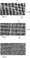
- Figure 2 shows an optical microscope picture of 15 ⁇ m thin glass fabric (Asahi Kasei E-materials).
- the glass fabric comprises woven yarn 10a-b of glass fibers.
- Each yarn includes a plurality of glass fibers, also denoted filaments.
- the diameter of a filament is typically 4 5 ⁇ m, and the number of filaments in the yarn is typically 50.
- the glass fabric has large holes 14 between the woven yarns, which would allow a large amount of the conductive particles in the printed ink to pass right through the woven fiber in an uncontrolled way. This is an unwanted effect.
- the size of the holes can be as large as 200 ⁇ m.
- non-woven glass fibers are disposed on top of the fabric. This can be done by soaking the fabric in a solution containing glass fibers and then removing the liquid part of the solution.
- Figure 3 shows an optical microscope picture of the glass fabric shown in figure 2 treated with 20 gram glass microfiber stock solution on both sides, corresponding to 0.04 milligrams of deposited glass fiber per square centimeter on each side.
- the woven yarn in the glass fabric is covered by the disposed non-woven glass fibers. It can also be seen from figure 3 that the size of the holes in the fabric is reduced. However, full coverage of the holes in the glass fabric is not accomplished.
- Figure 4 shows an optical microscope picture of the glass fabric shown in figure 2 treated with 80 gram glass microfiber stock solution on both sides, corresponding to 0.16 milligrams of deposited glass fiber per square centimeter on each side.
- the holes are now covered by the glass microfibers.
- full coverage of holes in the glass fabric can be achieved by increasing the amount of glass microfiber.
- a binder such as, e.g., inorganic binders such as, silicates, colloidal silica particles, silanes (e.g., linear silane or branched silane or cyclic silane), and colloidal Al 2 O 3 is added to the fiberstock solution containing the glass fibers, the non-woven glass fibers can stick stronger to the woven fibers. Additionally, the layer consisting of deposited non-woven will be stronger mechanically as such. Consequently, by adding a binder to the fiberstock solution it is possible to form a mechanically strong non-woven layer that adheres strongly to the woven glass fibers.
- inorganic binders such as, silicates, colloidal silica particles, silanes (e.g., linear silane or branched silane or cyclic silane), and colloidal Al 2 O 3
- a 15 ⁇ m thin glass fabric (Asahi Kasei E-materials), as shown in figure 2 , with 50 filaments , with a filament diameter of 4 ⁇ m, was laid on top of a stainless steel wire screen (33 cm x 33 cm) in a hand sheet former and a stock cylinder was put on top of the glass fabric and then closed and tightened.
- a glass microfiber stock solution was prepared by mixing 4000 grams of distilled water and 8 grams of glass microfibers (Johns Manville, special purpose type glass microfiber type 90, fiber diameter: 0.2 ⁇ m) and 400 grams of water based colloidal silica (a solution containing around 15 wt.% SiO2 in water) such that the final silica concentration was 1.4 wt.%.
- the mixing was performed using an Ultraturrax batch dispenser.
- the stock cylinder of the hand sheet former machine was filled with distilled water (containing 1.4 wt.% silica) up to a level of 350 mm above the surface of the wire screen.
- 80 grams of glass microfiber stock was poured into the hand sheet former machine.
- the glass fiber stock and the distilled water containing silica were mixed by compressed air for 4 seconds and then allowed to settle for 6 seconds, after which the water was drained through the glass fabric and the wire screen.
- the wet treated glass fabric was dried at 110°C in air in a belt oven.
- the glass fabric was then treated on the other side using the same process parameters as in the first treatment.
- the resulting substrate is shown in figure 4 .
- the woven yarn in the glass fabric is fully covered by the disposed non-woven glass microfibers.
- the thickness of the glass fabric with disposed glass microfibers was around 30 ⁇ m. This means that the total thickness of the two layers of non-woven microfibers is about 15 ⁇ m. By using a thinner glass fabric, it is possible to further reduce the thickness of the insulation substrate.
- Example 1 A variation of Example 1 is that the microfiber stock solution is prepared by mixing 4000 grams of distilled water and 200 grams of nanocellulose dispersion (water based nanocellulose dispersion containing 2% by weight of nanocellulose) and 400 grams of water based colloidal silica (a solution containing 15 wt.% SiO2 in water).
- the ceramic glass microfibers in the microfiber stock solution are replaced by organic microfibers consisting of nanocellulose. Using nanocellulose simplifies the manufacturing process in that dipping can be used instead of using a paper manufacturing process.
- microfiber stock solution is prepared by mixing 4000 grams of distilled water and 2 grams of glass microfibers (Johns Manville, special purpose type glass microfiber type 90, fiber diameter: 0.2 ⁇ m) and 200 grams of nanocellulose dispersion (water based nanocellulose dispersion containing 2% by weight of nanocellulose) and 400 grams of water based colloidal silica (a solution containing 15 wt.% SiO2 in water).
- glass microfibers Johns Manville, special purpose type glass microfiber type 90, fiber diameter: 0.2 ⁇ m
- nanocellulose dispersion water based nanocellulose dispersion containing 2% by weight of nanocellulose
- water based colloidal silica a solution containing 15 wt.% SiO2 in water
- ink with conductive particles is deposited on at least one side of the substrate on top of the layer of non-woven microfibers, to form a porous conducting layer on the porous insulation substrate.
- the ink is deposited on both sides of the substrate on top the layers of non-woven microfibers, to form a porous conducting layer on each side of the porous insulation substrate.
- the ink with conductive particles is only deposited on one side of the substrate.
- additives to the distilled water before mixing water and the microfibers.
- suitable additives are surfactants, dispersants, wetting agents, retention aids, defoamers, and rheology changing agents. It is advantageous to add one or more of those additives.
- the additives are burnt away during the following steps of the manufacturing process of the solar cell, and consequently do not remain in the end product.
- the purpose of the additives is to achieve individual and non-agglomerated fibers, so that the individual fibers can be deposited as homogeneously as possible in order to provide a thin and at the same time dense layer of individual fibers.
- additives it is possible to manufacture a thinner and denser substrate with smaller holes.
- a smoother and more homogeneous microfiber deposition can be accomplished. Further, it is advantageous to add a wetting agent to the fiberstock solution so that the dilution water wets the fibers and the fabric. Also, by adding a water soluble polymer to the fiberstock solution and the dilution water, a smoother and more homogeneous microfiber deposition can be accomplished. However, it was found that, when adding polymer it was necessary to add a defoaming agent in order to avoid excessive foaming during dilution water filling and agitation and draining cycles. It is also advantageous to add rheology changing additives to change the viscosity of the fiberstock solution and the dilution water.
- Binders that can be used are e.g. inorganic binders such as, silicates, colloidal silica particles, silane, e.g. linear silane, branched silane, or cyclic silane, and colloidal Al 2 O 3 .
- Nanocellulose can be used as a retention aid.
- Figure 5 shows a cross section through a porous insulation substrate 4 manufactured according to the method described in the example described above.
- the substrate has a layer 5 of woven microfibers including woven yarns 10 comprising a plurality of filaments 11 and holes 14 formed between the yarns 10.
- the woven yarns 10 are preferably made of ceramic microfibers.
- the substrate also includes two layers 6, 7 of non-woven microfibers arranged on each side of the layer 5 of woven microfibers.
- the layers 6, 7 of non-woven microfibers can be made of ceramic microfibers, organic microfibers or a combination thereof. As can be seen from the figure, a main part of the non-woven microfibers are accumulated in the holes 14 between the yarns 10.
- the side of the non-woven layer 6, 7 that faces away from the woven layer 5 is smooth, but the opposite side of the non-woven layer that faces against the woven layer is uneven and has thick parts 16 that protrude into the holes 14 of the woven layer and thin parts 17, which are disposed on top of the yarns 10.
- the present invention can be used for monolithic as well as sandwich types of DCS.
- the non-woven microfibers should preferably be thinner than the filaments in the layer of woven microfibers.
- the fibers in the layer of non-woven microfibers should have a diameter less than 4 ⁇ m, preferably less than 1 ⁇ m, and more preferably less than 0.5 ⁇ m in order to block the holes in an efficient way.
- the length of the non-woven fibers is, for example 100 nm - 3 mm.
- the diameter of nano-cellulose fibers is typically 5 -10 nm and the length of the fibers is typically several ⁇ m.
- nano-cellulose fibers having a diameter of 10 - 20 nm and a length of several mm.
- the microfiber stock solution may include microfibers of different materials and diameters.
- the examples above use glass microfibers, the invention is not limited to glass microfibers. It is possible to use other types of ceramic microfibers with similar properties.
- the microfibers in the non-woven layer can be made of a different ceramic material than the microfibers in the woven layer.
- the microfibers in the non-woven layer can be made of organic microfiber such as cellulose or polymer.
- the substrate may include a layer of non-woven microfibers and a layer of woven microfibers laminated together.
- the substrate has only one layer of non-woven microfibers, arranged on one side of a layer of woven microfibers. Although it is advantageous to have non-woven layers on both sides of the woven layer, it is not necessary. It is possible to deposit conducting layers on both sides of the substrate although only one of the sides of the woven layer has been provided with a layer of non-woven microfibers.
- the conducting layer can be printed on the non-woven layer as well as on the woven layer.
- a substrate having non-woven layers deposited on both sides of the woven layer can be covered with a conducting layer on one side as well as on both sides.
- the porous insulation substrate has only one layer of non-woven microfibers, arranged on one side of a layer of woven microfibers and the conducting layer is deposited on the other side of the woven microfibers, i.e. the conducting layer is deposited on the woven microfibers and not on the non-woven microfibers.
- the porous insulating substrate is a porous and chemically inert and high temperature resistant and electrically insulating material that can be used for other applications than in dye-sensitized solar cells.
- the substrate can be used in filtering/filter applications for removing, e.g. dust, organic or inorganic or biological micro particles, flour, sand, smoke, bacteria, and pollen.
- the substrate can also be used as a separator, materially separating the cathode and anode in electrochemical- or photoelectrochemical devices such as fuel cells, batteries, electrochemical sensors, electrochromic displays, and photoelectrochemical solar cells.
- electrochemical- or photoelectrochemical devices such as fuel cells, batteries, electrochemical sensors, electrochromic displays, and photoelectrochemical solar cells.
- Binders that can be used are e.g. inorganic binders such as, silicates, colloidal silica particles, silane, e.g. linear silane, branched silane, or cyclic silane, and colloidal Al 2 O 3 .
- Nanocellulose can be used as a retention aid.
- Figure 5 shows a cross section through a porous insulation substrate 4 manufactured according to the method described in the example described above.
- the substrate has a layer 5 of woven microfibers including woven yarns 10 comprising a plurality of filaments 11 and holes 14 formed between the yarns 10.
- the woven yarns 10 are preferably made of ceramic microfibers.
- the substrate also includes two layers 6, 7 of non-woven microfibers arranged on each side of the layer 5 of woven microfibers.
- the layers 6, 7 of non-woven microfibers can be made of ceramic microfibers, organic microfibers or a combination thereof. As can be seen from the figure, a main part of the non-woven microfibers are accumulated in the holes 14 between the yarns 10.
- the thickness of the non-woven layers 6, 7 of microfibers varies in dependence of the locations of the holes 14 in the woven layer of microfibers, such that the non-woven layer is thicker in the holes 14 in the woven layer and thinner on top of the yarns 17 of the woven layer.
- the side of the non-woven layer 6, 7 that faces away from the woven layer 5 is smooth, but the opposite side of the non-woven layer that faces against the woven layer is uneven and has thick parts 16 that protrude into the holes 14 of the woven layer and thin parts 17, which are disposed on top of the yarns 10.
- the present invention can be used for monolithic as well as sandwich types of DCS.
- the non-woven microfibers should preferably be thinner than the filaments in the layer of woven microfibers.
- the fibers in the layer of non-woven microfibers should have a diameter less than 4 ⁇ m, preferably less than 1 ⁇ m, and more preferably less than 0.5 ⁇ m in order to block the holes in an efficient way.
- the length of the non-woven fibers is, for example 100 nm - 3 mm.
- the diameter of nano-cellulose fibers is typically 5 -10 nm and the length of the fibers is typically several ⁇ m.
- nano-cellulose fibers having a diameter of 10 - 20 nm and a length of several mm.
- the microfiber stock solution may include microfibers of different materials and diameters.
- the examples above use glass microfibers, the invention is not limited to glass microfibers. It is possible to use other types of ceramic microfibers with similar properties.
- the microfibers in the non-woven layer can be made of a different ceramic material than the microfibers in the woven layer.
- the microfibers in the non-woven layer can be made of organic microfiber such as cellulose or polymer.
- the substrate may include a layer of non-woven microfibers and a layer of woven microfibers laminated together.
- the substrate has only one layer of non-woven microfibers, arranged on one side of a layer of woven microfibers. Although it is advantageous to have non-woven layers on both sides of the woven layer, it is not necessary. It is possible to deposit conducting layers on both sides of the substrate although only one of the sides of the woven layer has been provided with a layer of non-woven microfibers.
- the conducting layer can be printed on the non-woven layer as well as on the woven layer.
- a substrate having non-woven layers deposited on both sides of the woven layer can be covered with a conducting layer on one side as well as on both sides.
- the porous insulation substrate has only one layer of non-woven microfibers, arranged on one side of a layer of woven microfibers and the conducting layer is deposited on the other side of the woven microfibers, i.e. the conducting layer is deposited on the woven microfibers and not on the non-woven microfibers.
- the porous insulating substrate is a porous and chemically inert and high temperature resistant and electrically insulating material that can be used for other applications than in dye-sensitized solar cells.
- the substrate can be used in filtering/filter applications for removing, e.g. dust, organic or inorganic or biological micro particles, flour, sand, smoke, bacteria, and pollen.
- the substrate can also be used as a separator, materially separating the cathode and anode in electrochemical- or photoelectrochemical devices such as fuel cells, batteries, electrochemical sensors, electrochromic displays, and photoelectrochemical solar cells.
- electrochemical- or photoelectrochemical devices such as fuel cells, batteries, electrochemical sensors, electrochromic displays, and photoelectrochemical solar cells.
Landscapes
- Engineering & Computer Science (AREA)
- Power Engineering (AREA)
- Microelectronics & Electronic Packaging (AREA)
- Textile Engineering (AREA)
- Manufacturing & Machinery (AREA)
- Electrochemistry (AREA)
- Chemical Kinetics & Catalysis (AREA)
- Chemical & Material Sciences (AREA)
- Life Sciences & Earth Sciences (AREA)
- Wood Science & Technology (AREA)
- Hybrid Cells (AREA)
- Photovoltaic Devices (AREA)
- Laminated Bodies (AREA)
Claims (10)
- Substrat poreux d'isolation constitué de microfibres, dans lequel le substrat poreux d'isolation comprend une couche (5) de microfibres tissées, la couche de microfibres tissées comprend des fils de microfibres tissées séparés par des trous (14) entre eux, et une couche (6) de microfibres non tissées disposée sur la couche de microfibres tissées sur un premier côté, caractérisé en ce qu'au moins une partie des microfibres non tissées sont accumulées dans les trous entre les fils et l'épaisseur de la couche (6) de microfibres non tissées varie en fonction des emplacements des trous (14) dans la couche (5) de microfibres tissées de telle sorte que la couche (6) de microfibres non tissées est plus épaisse dans lesdits trous et est plus mince sur le dessus des fils de la couche de microfibres tissées, dans lequel les fils (10) incluent une pluralité de filaments (11) et le diamètre desdites microfibres non tissées est plus petit que le diamètre desdits filaments.
- Substrat poreux d'isolation selon la revendication 1, dans lequel le substrat poreux d'isolation (4) comprend une deuxième couche (7) de microfibres non tissées disposée sur un deuxième côté de la couche (5) de microfibres tissées.
- Substrat poreux d'isolation selon l'une quelconque des revendications précédentes, dans lequel ladite couche (5) de microfibres tissées est constituée d'un tissu de verre, et les fibres dans ladite couche (6) de microfibres non tissées sont constituées de verre.
- Substrat poreux d'isolation selon l'une quelconque des revendications précédentes, dans lequel l'épaisseur de ladite couche (5) de microfibres tissées est comprise entre 4 µm et 30 µm, de préférence entre 4 µm et 20 µm et plus préférablement entre 4 µm et 10 µm.
- Substrat poreux d'isolation selon l'une quelconque des revendications précédentes, dans lequel les microfibres dans la couche (6, 7) de microfibres non tissées ont un diamètre inférieur à 4 µm, de préférence inférieur à 1 µm, et plus préférablement inférieur à 0,5 µm.
- Substrat poreux d'isolation selon l'une quelconque des revendications précédentes, dans lequel ladite couche (5) de microfibres tissées et la couche (6, 7) de microfibres non tissées sont constituées de microfibres céramiques.
- Substrat poreux d'isolation selon l'une quelconque des revendications précédentes, dans lequel ladite couche (6, 7) de microfibres non tissées comprend des microfibres organiques.
- Substrat poreux d'isolation selon l'une quelconque des revendications précédentes, dans lequel ladite couche (6, 7) de microfibres non tissées est constituée de nanocellulose.
- Substrat poreux d'isolation selon l'une quelconque des revendications précédentes, dans lequel ladite couche (6, 7) de microfibres non tissées comprend des microfibres organiques et des microfibres céramiques.
- Substrat poreux d'isolation selon l'une quelconque des revendications précédentes, dans lequel ladite couche (6, 7) de microfibres non tissées comprend des microfibres organiques et des microfibres de verre.
Applications Claiming Priority (4)
| Application Number | Priority Date | Filing Date | Title |
|---|---|---|---|
| SE1230033A SE537669C2 (sv) | 2012-04-04 | 2012-04-04 | Färgämnessensiterad solcellsmodul med seriekopplad struktursamt sätt för framställning av solcellen |
| SE1200791A SE537449C2 (sv) | 2012-04-04 | 2012-12-28 | En färgämnessensiterad solcell som innehåller ett poröst isolerande substrat samt en metod för framställning av det porösa isolerande substratet |
| EP13710341.2A EP2834824B1 (fr) | 2012-04-04 | 2013-03-08 | Cellule solaire à colorant comprenant un substrat isolant poreux |
| PCT/EP2013/054790 WO2013149789A2 (fr) | 2012-04-04 | 2013-03-08 | Cellule solaire traitée par colorant sensibilisateur comprenant un substrat isolant poreux et procédé de production dudit substrat poreux isolant |
Related Parent Applications (2)
| Application Number | Title | Priority Date | Filing Date |
|---|---|---|---|
| EP13710341.2A Division EP2834824B1 (fr) | 2012-04-04 | 2013-03-08 | Cellule solaire à colorant comprenant un substrat isolant poreux |
| EP13710341.2A Division-Into EP2834824B1 (fr) | 2012-04-04 | 2013-03-08 | Cellule solaire à colorant comprenant un substrat isolant poreux |
Publications (2)
| Publication Number | Publication Date |
|---|---|
| EP3159155A1 EP3159155A1 (fr) | 2017-04-26 |
| EP3159155B1 true EP3159155B1 (fr) | 2021-11-10 |
Family
ID=47901048
Family Applications (2)
| Application Number | Title | Priority Date | Filing Date |
|---|---|---|---|
| EP13710341.2A Active EP2834824B1 (fr) | 2012-04-04 | 2013-03-08 | Cellule solaire à colorant comprenant un substrat isolant poreux |
| EP16203369.0A Active EP3159155B1 (fr) | 2012-04-04 | 2013-03-08 | Cellule solaire sensibilisée par colorant comprenant un substrat composite |
Family Applications Before (1)
| Application Number | Title | Priority Date | Filing Date |
|---|---|---|---|
| EP13710341.2A Active EP2834824B1 (fr) | 2012-04-04 | 2013-03-08 | Cellule solaire à colorant comprenant un substrat isolant poreux |
Country Status (14)
| Country | Link |
|---|---|
| US (3) | US9190218B2 (fr) |
| EP (2) | EP2834824B1 (fr) |
| JP (1) | JP5978385B2 (fr) |
| KR (1) | KR101675658B1 (fr) |
| CN (3) | CN104637693B (fr) |
| AU (1) | AU2013242933B2 (fr) |
| BR (1) | BR112014024935B1 (fr) |
| CA (1) | CA2866779C (fr) |
| ES (2) | ES2761201T3 (fr) |
| MX (1) | MX340471B (fr) |
| RU (2) | RU2654521C1 (fr) |
| SE (1) | SE537449C2 (fr) |
| WO (1) | WO2013149789A2 (fr) |
| ZA (1) | ZA201406791B (fr) |
Families Citing this family (12)
| Publication number | Priority date | Publication date | Assignee | Title |
|---|---|---|---|---|
| EP3598465A1 (fr) * | 2018-07-16 | 2020-01-22 | Exeger Operations AB | Cellule photovoltaique avec support en tissu et chargeur pour appareils électroniques portables |
| US10964486B2 (en) | 2013-05-17 | 2021-03-30 | Exeger Operations Ab | Dye-sensitized solar cell unit and a photovoltaic charger including the solar cell unit |
| SE537836C2 (sv) | 2014-02-06 | 2015-11-03 | Exeger Sweden Ab | En transparent färgämnessensibiliserad solcell samt ett sättför framställning av densamma |
| KR101554992B1 (ko) * | 2014-11-12 | 2015-09-23 | 한국전기연구원 | 섬유직조체를 포함하는 염료감응형 태양전지 |
| KR102310356B1 (ko) * | 2015-03-24 | 2021-10-07 | 한국전기연구원 | 쇼트방지 전극을 삽입가능한 염료감응형 태양전지 |
| EP3503141B1 (fr) | 2017-12-21 | 2022-01-26 | Exeger Operations AB | Cellule solaire et son procédé de fabrication |
| TWI780213B (zh) * | 2018-05-16 | 2022-10-11 | 瑞典商艾克瑟格操作公司 | 用於充電電子裝置的光伏充電器、製造該光伏充電器的方法及該光伏充電器作為充電電子裝置之用途 |
| JP6952207B2 (ja) * | 2018-05-16 | 2021-10-20 | エクセジャー オペレーションズ エービー | 光起電力装置 |
| CN109004089B (zh) * | 2018-07-11 | 2020-02-18 | 华南理工大学 | 3d气凝胶喷射打印制备可卷曲式纳米纸基柔性太阳能电池的方法 |
| CN111048791B (zh) * | 2018-10-11 | 2024-10-29 | 宁德时代新能源科技股份有限公司 | 二次电池及其电极构件 |
| EP4060699A1 (fr) | 2021-03-18 | 2022-09-21 | Exeger Operations AB | Cellule solaire et son procédé de fabrication |
| PL4060698T3 (pl) * | 2021-03-18 | 2023-09-18 | Exeger Operations Ab | Ogniwo słoneczne zawierające wielość porowatych warstw i nośnik do przewodzenia ładunku penetrujący porowate warstwy |
Family Cites Families (42)
| Publication number | Priority date | Publication date | Assignee | Title |
|---|---|---|---|---|
| US3949130A (en) * | 1974-01-04 | 1976-04-06 | Tuff Spun Products, Inc. | Spun bonded fabric, and articles made therefrom |
| GB1603519A (en) * | 1978-01-23 | 1981-11-25 | Process Scient Innovations | Filter elements for gas or liquid and methods of making such filters |
| US4293378A (en) * | 1980-01-10 | 1981-10-06 | Max Klein | Enhanced wet strength filter mats to separate particulates from fluids and/or coalesce entrained droplets from gases |
| US4397907A (en) * | 1981-06-22 | 1983-08-09 | Hughes Aircraft Company | Multi-purpose air permeable composites |
| US4734208A (en) * | 1981-10-19 | 1988-03-29 | Pall Corporation | Charge-modified microfiber filter sheets |
| US4885217A (en) * | 1987-07-06 | 1989-12-05 | Alupower, Inc. | Air cathodes and materials therefor |
| JPH076077B2 (ja) * | 1989-10-16 | 1995-01-25 | 片山特殊工業株式会社 | 金属多孔体の製造方法および該方法により製造された金属多孔体 |
| DE68925580T2 (de) * | 1989-04-14 | 1996-09-19 | Katayama Tokushu Kogyo Kk | Verfahren zur Herstellung einer porösen metallischen Folie |
| US5631099A (en) * | 1995-09-21 | 1997-05-20 | Hockaday; Robert G. | Surface replica fuel cell |
| US6183898B1 (en) | 1995-11-28 | 2001-02-06 | Hoescht Research & Technology Deutschland Gmbh & Co. Kg | Gas diffusion electrode for polymer electrolyte membrane fuel cells |
| DE19544323A1 (de) * | 1995-11-28 | 1997-06-05 | Magnet Motor Gmbh | Gasdiffusionselektrode für Polymerelektrolytmembran-Brennstoffzellen |
| EP0859386A1 (fr) | 1997-02-17 | 1998-08-19 | Monsanto Company | Cellule photovoltaique |
| DE69828802T2 (de) * | 1997-09-03 | 2005-12-22 | Asahi Kasei Kabushiki Kaisha | Polyesterfaser und gewebe daraus |
| US20080011350A1 (en) * | 1999-03-30 | 2008-01-17 | Daniel Luch | Collector grid, electrode structures and interconnect structures for photovoltaic arrays and other optoelectric devices |
| EP1114482B1 (fr) * | 1999-07-01 | 2003-05-28 | Squirrel Holdings Ltd. | Electrode bipolaire pour reactions electrochimiques d'oxydoreduction |
| CA2392984A1 (fr) | 1999-12-15 | 2001-06-21 | Hollingsworth & Vose Company | Filtres en microfibres de verre possedant une teneur limitee en bore |
| JP4705746B2 (ja) * | 2000-05-23 | 2011-06-22 | ジーイー・オズモニクス・インコーポレイテッド | ナノ濾過のための酸安定性膜 |
| US20020123283A1 (en) * | 2000-11-07 | 2002-09-05 | The Procter & Gamble Company | Foam materials derived from high internal phase emulsions for clothing insulation |
| US6872311B2 (en) * | 2002-01-31 | 2005-03-29 | Koslow Technologies Corporation | Nanofiber filter media |
| US7341618B2 (en) * | 2002-10-24 | 2008-03-11 | Georgia Tech Research Corporation | Filters and methods of making and using the same |
| US20040224594A1 (en) | 2003-04-18 | 2004-11-11 | Choi Wai Ming | Low density nonwoven glass fiber web |
| JP2005158470A (ja) * | 2003-11-25 | 2005-06-16 | Ngk Spark Plug Co Ltd | 色素増感型太陽電池 |
| US7233829B2 (en) * | 2004-03-03 | 2007-06-19 | Glycon Technologies, L.L.C. | Electric field shark repellent wet suit |
| JP2005317453A (ja) * | 2004-04-30 | 2005-11-10 | Ngk Spark Plug Co Ltd | 色素増感型太陽電池及びその製造方法 |
| US20060166582A1 (en) * | 2005-01-24 | 2006-07-27 | Turkson Abraham K | Composite higher temperature needlefelts with woven fiberglass scrims |
| JP4863662B2 (ja) * | 2005-07-06 | 2012-01-25 | シャープ株式会社 | 色素増感型太陽電池モジュールおよびその製造方法 |
| US7964012B2 (en) * | 2005-08-03 | 2011-06-21 | Hollingsworth & Vose Company | Filter media with improved conductivity |
| FI119280B (fi) * | 2006-05-18 | 2008-09-30 | Valtion Teknillinen | Suodatin ja uudet menetelmät |
| DE102006023638A1 (de) * | 2006-05-18 | 2007-11-22 | Sefar Ag | Photovoltaische Zelle |
| US20080176050A1 (en) * | 2006-12-01 | 2008-07-24 | Lydall, Inc. | Gypsum wallboard facings |
| US20100279569A1 (en) * | 2007-01-03 | 2010-11-04 | Lockheed Martin Corporation | Cnt-infused glass fiber materials and process therefor |
| JP2008218125A (ja) | 2007-03-02 | 2008-09-18 | Matsushita Electric Ind Co Ltd | リチウムイオン二次電池用負極およびリチウムイオン二次電池 |
| JP2009076448A (ja) * | 2007-08-28 | 2009-04-09 | Toray Ind Inc | 色素増感型太陽電池 |
| EP2452350A1 (fr) * | 2009-07-09 | 2012-05-16 | NLAB Solar AB | Cellule solaire à colorant dotée de caractéristiques optiques améliorées |
| KR20110066164A (ko) * | 2009-08-07 | 2011-06-16 | 파나소닉 주식회사 | 비수성 전해질 이차 전지 |
| JP5678345B2 (ja) * | 2010-02-03 | 2015-03-04 | 新日鉄住金化学株式会社 | 色素増感太陽電池およびその製造方法 |
| JP4803305B2 (ja) * | 2010-03-30 | 2011-10-26 | 大日本印刷株式会社 | 色素増感型太陽電池 |
| JP5815509B2 (ja) * | 2010-04-29 | 2015-11-17 | 新日鉄住金化学株式会社 | 色素増感太陽電池および色素増感太陽電池モジュール |
| JP2012009374A (ja) * | 2010-06-28 | 2012-01-12 | Sharp Corp | 色素増感太陽電池およびその製造方法、並びに色素増感太陽電池モジュール |
| JP2012048863A (ja) * | 2010-08-24 | 2012-03-08 | Sony Corp | 色素増感太陽電池及び色素増感太陽電池製造方法 |
| JP2012084374A (ja) * | 2010-10-12 | 2012-04-26 | Sony Corp | 光電変換素子、光電変換素子の製造方法、光電変換素子用電解質層および電子機器 |
| JP2012204046A (ja) * | 2011-03-24 | 2012-10-22 | Sony Corp | 光電変換装置及びその製造方法 |
-
2012
- 2012-12-28 SE SE1200791A patent/SE537449C2/sv unknown
-
2013
- 2013-03-08 ES ES13710341T patent/ES2761201T3/es active Active
- 2013-03-08 EP EP13710341.2A patent/EP2834824B1/fr active Active
- 2013-03-08 MX MX2014012018A patent/MX340471B/es active IP Right Grant
- 2013-03-08 CN CN201510083212.5A patent/CN104637693B/zh active Active
- 2013-03-08 EP EP16203369.0A patent/EP3159155B1/fr active Active
- 2013-03-08 CA CA2866779A patent/CA2866779C/fr active Active
- 2013-03-08 KR KR1020147030945A patent/KR101675658B1/ko active Active
- 2013-03-08 JP JP2015503797A patent/JP5978385B2/ja active Active
- 2013-03-08 RU RU2016151318A patent/RU2654521C1/ru active
- 2013-03-08 WO PCT/EP2013/054790 patent/WO2013149789A2/fr not_active Ceased
- 2013-03-08 CN CN201380017889.8A patent/CN104221108B/zh active Active
- 2013-03-08 BR BR112014024935-0A patent/BR112014024935B1/pt not_active IP Right Cessation
- 2013-03-08 CN CN201710068087.XA patent/CN106847515A/zh active Pending
- 2013-03-08 US US14/390,804 patent/US9190218B2/en active Active
- 2013-03-08 RU RU2014144280A patent/RU2609775C2/ru active
- 2013-03-08 AU AU2013242933A patent/AU2013242933B2/en active Active
- 2013-03-08 ES ES16203369T patent/ES2902708T3/es active Active
-
2014
- 2014-09-16 ZA ZA2014/06791A patent/ZA201406791B/en unknown
-
2015
- 2015-10-09 US US14/879,668 patent/US10256047B2/en active Active
-
2017
- 2017-05-03 US US15/585,549 patent/US10249445B2/en active Active
Non-Patent Citations (1)
| Title |
|---|
| None * |
Also Published As
Similar Documents
| Publication | Publication Date | Title |
|---|---|---|
| EP3159155B1 (fr) | Cellule solaire sensibilisée par colorant comprenant un substrat composite | |
| US10971312B2 (en) | Dye-sensitized solar cell and a method for manufacturing the solar cell | |
| JP7669634B2 (ja) | 複数の多孔質層及び多孔質層に浸透する電荷伝導媒体を備えるソーラーセル | |
| HK1204708B (en) | A dye-sensitized solar cell including a composite substrate | |
| TW202349735A (zh) | 包括多個多孔層和穿透該多孔層的電荷傳導介質的太陽能電池 | |
| BR122017005957A2 (pt) | célula solar sensibilizada por corante incluindo um substrato poroso isolante e método para produção do substrato poroso isolante | |
| OA21555A (en) | A solar cell comprising a plurality of porous layers and charge conducting medium penetrating the porous layers. | |
| EA046404B1 (ru) | Элемент солнечной батареи, содержащий пористые слои и проводящую заряд среду, проникающую через пористые слои |
Legal Events
| Date | Code | Title | Description |
|---|---|---|---|
| PUAI | Public reference made under article 153(3) epc to a published international application that has entered the european phase |
Free format text: ORIGINAL CODE: 0009012 |
|
| STAA | Information on the status of an ep patent application or granted ep patent |
Free format text: STATUS: REQUEST FOR EXAMINATION WAS MADE |
|
| 17P | Request for examination filed |
Effective date: 20161212 |
|
| AC | Divisional application: reference to earlier application |
Ref document number: 2834824 Country of ref document: EP Kind code of ref document: P |
|
| AK | Designated contracting states |
Kind code of ref document: A1 Designated state(s): AL AT BE BG CH CY CZ DE DK EE ES FI FR GB GR HR HU IE IS IT LI LT LU LV MC MK MT NL NO PL PT RO RS SE SI SK SM TR |
|
| RBV | Designated contracting states (corrected) |
Designated state(s): AL AT BE BG CH CY CZ DE DK EE ES FI FR GB GR HR HU IE IS IT LI LT LU LV MC MK MT NL NO PL PT RO RS SE SI SK SM TR |
|
| RAP1 | Party data changed (applicant data changed or rights of an application transferred) |
Owner name: EXEGER OPERATIONS AB |
|
| STAA | Information on the status of an ep patent application or granted ep patent |
Free format text: STATUS: EXAMINATION IS IN PROGRESS |
|
| 17Q | First examination report despatched |
Effective date: 20201203 |
|
| GRAP | Despatch of communication of intention to grant a patent |
Free format text: ORIGINAL CODE: EPIDOSNIGR1 |
|
| STAA | Information on the status of an ep patent application or granted ep patent |
Free format text: STATUS: GRANT OF PATENT IS INTENDED |
|
| INTG | Intention to grant announced |
Effective date: 20210709 |
|
| GRAS | Grant fee paid |
Free format text: ORIGINAL CODE: EPIDOSNIGR3 |
|
| GRAA | (expected) grant |
Free format text: ORIGINAL CODE: 0009210 |
|
| STAA | Information on the status of an ep patent application or granted ep patent |
Free format text: STATUS: THE PATENT HAS BEEN GRANTED |
|
| AC | Divisional application: reference to earlier application |
Ref document number: 2834824 Country of ref document: EP Kind code of ref document: P |
|
| AK | Designated contracting states |
Kind code of ref document: B1 Designated state(s): AL AT BE BG CH CY CZ DE DK EE ES FI FR GB GR HR HU IE IS IT LI LT LU LV MC MK MT NL NO PL PT RO RS SE SI SK SM TR |
|
| REG | Reference to a national code |
Ref country code: GB Ref legal event code: FG4D |
|
| REG | Reference to a national code |
Ref country code: AT Ref legal event code: REF Ref document number: 1445700 Country of ref document: AT Kind code of ref document: T Effective date: 20211115 Ref country code: CH Ref legal event code: EP |
|
| REG | Reference to a national code |
Ref country code: DE Ref legal event code: R096 Ref document number: 602013080032 Country of ref document: DE |
|
| REG | Reference to a national code |
Ref country code: IE Ref legal event code: FG4D |
|
| REG | Reference to a national code |
Ref country code: SE Ref legal event code: TRGR |
|
| REG | Reference to a national code |
Ref country code: LT Ref legal event code: MG9D |
|
| REG | Reference to a national code |
Ref country code: NL Ref legal event code: MP Effective date: 20211110 |
|
| REG | Reference to a national code |
Ref country code: ES Ref legal event code: FG2A Ref document number: 2902708 Country of ref document: ES Kind code of ref document: T3 Effective date: 20220329 |
|
| REG | Reference to a national code |
Ref country code: AT Ref legal event code: MK05 Ref document number: 1445700 Country of ref document: AT Kind code of ref document: T Effective date: 20211110 |
|
| PG25 | Lapsed in a contracting state [announced via postgrant information from national office to epo] |
Ref country code: RS Free format text: LAPSE BECAUSE OF FAILURE TO SUBMIT A TRANSLATION OF THE DESCRIPTION OR TO PAY THE FEE WITHIN THE PRESCRIBED TIME-LIMIT Effective date: 20211110 Ref country code: LT Free format text: LAPSE BECAUSE OF FAILURE TO SUBMIT A TRANSLATION OF THE DESCRIPTION OR TO PAY THE FEE WITHIN THE PRESCRIBED TIME-LIMIT Effective date: 20211110 Ref country code: FI Free format text: LAPSE BECAUSE OF FAILURE TO SUBMIT A TRANSLATION OF THE DESCRIPTION OR TO PAY THE FEE WITHIN THE PRESCRIBED TIME-LIMIT Effective date: 20211110 Ref country code: BG Free format text: LAPSE BECAUSE OF FAILURE TO SUBMIT A TRANSLATION OF THE DESCRIPTION OR TO PAY THE FEE WITHIN THE PRESCRIBED TIME-LIMIT Effective date: 20220210 Ref country code: AT Free format text: LAPSE BECAUSE OF FAILURE TO SUBMIT A TRANSLATION OF THE DESCRIPTION OR TO PAY THE FEE WITHIN THE PRESCRIBED TIME-LIMIT Effective date: 20211110 |
|
| PG25 | Lapsed in a contracting state [announced via postgrant information from national office to epo] |
Ref country code: IS Free format text: LAPSE BECAUSE OF FAILURE TO SUBMIT A TRANSLATION OF THE DESCRIPTION OR TO PAY THE FEE WITHIN THE PRESCRIBED TIME-LIMIT Effective date: 20220310 Ref country code: PT Free format text: LAPSE BECAUSE OF FAILURE TO SUBMIT A TRANSLATION OF THE DESCRIPTION OR TO PAY THE FEE WITHIN THE PRESCRIBED TIME-LIMIT Effective date: 20220310 Ref country code: PL Free format text: LAPSE BECAUSE OF FAILURE TO SUBMIT A TRANSLATION OF THE DESCRIPTION OR TO PAY THE FEE WITHIN THE PRESCRIBED TIME-LIMIT Effective date: 20211110 Ref country code: NO Free format text: LAPSE BECAUSE OF FAILURE TO SUBMIT A TRANSLATION OF THE DESCRIPTION OR TO PAY THE FEE WITHIN THE PRESCRIBED TIME-LIMIT Effective date: 20220210 Ref country code: NL Free format text: LAPSE BECAUSE OF FAILURE TO SUBMIT A TRANSLATION OF THE DESCRIPTION OR TO PAY THE FEE WITHIN THE PRESCRIBED TIME-LIMIT Effective date: 20211110 Ref country code: LV Free format text: LAPSE BECAUSE OF FAILURE TO SUBMIT A TRANSLATION OF THE DESCRIPTION OR TO PAY THE FEE WITHIN THE PRESCRIBED TIME-LIMIT Effective date: 20211110 Ref country code: HR Free format text: LAPSE BECAUSE OF FAILURE TO SUBMIT A TRANSLATION OF THE DESCRIPTION OR TO PAY THE FEE WITHIN THE PRESCRIBED TIME-LIMIT Effective date: 20211110 Ref country code: GR Free format text: LAPSE BECAUSE OF FAILURE TO SUBMIT A TRANSLATION OF THE DESCRIPTION OR TO PAY THE FEE WITHIN THE PRESCRIBED TIME-LIMIT Effective date: 20220211 |
|
| PG25 | Lapsed in a contracting state [announced via postgrant information from national office to epo] |
Ref country code: SM Free format text: LAPSE BECAUSE OF FAILURE TO SUBMIT A TRANSLATION OF THE DESCRIPTION OR TO PAY THE FEE WITHIN THE PRESCRIBED TIME-LIMIT Effective date: 20211110 Ref country code: SK Free format text: LAPSE BECAUSE OF FAILURE TO SUBMIT A TRANSLATION OF THE DESCRIPTION OR TO PAY THE FEE WITHIN THE PRESCRIBED TIME-LIMIT Effective date: 20211110 Ref country code: RO Free format text: LAPSE BECAUSE OF FAILURE TO SUBMIT A TRANSLATION OF THE DESCRIPTION OR TO PAY THE FEE WITHIN THE PRESCRIBED TIME-LIMIT Effective date: 20211110 Ref country code: EE Free format text: LAPSE BECAUSE OF FAILURE TO SUBMIT A TRANSLATION OF THE DESCRIPTION OR TO PAY THE FEE WITHIN THE PRESCRIBED TIME-LIMIT Effective date: 20211110 Ref country code: DK Free format text: LAPSE BECAUSE OF FAILURE TO SUBMIT A TRANSLATION OF THE DESCRIPTION OR TO PAY THE FEE WITHIN THE PRESCRIBED TIME-LIMIT Effective date: 20211110 Ref country code: CZ Free format text: LAPSE BECAUSE OF FAILURE TO SUBMIT A TRANSLATION OF THE DESCRIPTION OR TO PAY THE FEE WITHIN THE PRESCRIBED TIME-LIMIT Effective date: 20211110 |
|
| REG | Reference to a national code |
Ref country code: DE Ref legal event code: R097 Ref document number: 602013080032 Country of ref document: DE |
|
| PLBE | No opposition filed within time limit |
Free format text: ORIGINAL CODE: 0009261 |
|
| STAA | Information on the status of an ep patent application or granted ep patent |
Free format text: STATUS: NO OPPOSITION FILED WITHIN TIME LIMIT |
|
| 26N | No opposition filed |
Effective date: 20220811 |
|
| PG25 | Lapsed in a contracting state [announced via postgrant information from national office to epo] |
Ref country code: MC Free format text: LAPSE BECAUSE OF FAILURE TO SUBMIT A TRANSLATION OF THE DESCRIPTION OR TO PAY THE FEE WITHIN THE PRESCRIBED TIME-LIMIT Effective date: 20211110 Ref country code: AL Free format text: LAPSE BECAUSE OF FAILURE TO SUBMIT A TRANSLATION OF THE DESCRIPTION OR TO PAY THE FEE WITHIN THE PRESCRIBED TIME-LIMIT Effective date: 20211110 |
|
| PG25 | Lapsed in a contracting state [announced via postgrant information from national office to epo] |
Ref country code: SI Free format text: LAPSE BECAUSE OF FAILURE TO SUBMIT A TRANSLATION OF THE DESCRIPTION OR TO PAY THE FEE WITHIN THE PRESCRIBED TIME-LIMIT Effective date: 20211110 |
|
| REG | Reference to a national code |
Ref country code: BE Ref legal event code: MM Effective date: 20220331 |
|
| PG25 | Lapsed in a contracting state [announced via postgrant information from national office to epo] |
Ref country code: LU Free format text: LAPSE BECAUSE OF NON-PAYMENT OF DUE FEES Effective date: 20220308 Ref country code: IE Free format text: LAPSE BECAUSE OF NON-PAYMENT OF DUE FEES Effective date: 20220308 |
|
| PG25 | Lapsed in a contracting state [announced via postgrant information from national office to epo] |
Ref country code: BE Free format text: LAPSE BECAUSE OF NON-PAYMENT OF DUE FEES Effective date: 20220331 |
|
| P01 | Opt-out of the competence of the unified patent court (upc) registered |
Effective date: 20230602 |
|
| PG25 | Lapsed in a contracting state [announced via postgrant information from national office to epo] |
Ref country code: HU Free format text: LAPSE BECAUSE OF FAILURE TO SUBMIT A TRANSLATION OF THE DESCRIPTION OR TO PAY THE FEE WITHIN THE PRESCRIBED TIME-LIMIT; INVALID AB INITIO Effective date: 20130308 |
|
| PG25 | Lapsed in a contracting state [announced via postgrant information from national office to epo] |
Ref country code: MK Free format text: LAPSE BECAUSE OF FAILURE TO SUBMIT A TRANSLATION OF THE DESCRIPTION OR TO PAY THE FEE WITHIN THE PRESCRIBED TIME-LIMIT Effective date: 20211110 Ref country code: CY Free format text: LAPSE BECAUSE OF FAILURE TO SUBMIT A TRANSLATION OF THE DESCRIPTION OR TO PAY THE FEE WITHIN THE PRESCRIBED TIME-LIMIT Effective date: 20211110 |
|
| PG25 | Lapsed in a contracting state [announced via postgrant information from national office to epo] |
Ref country code: TR Free format text: LAPSE BECAUSE OF FAILURE TO SUBMIT A TRANSLATION OF THE DESCRIPTION OR TO PAY THE FEE WITHIN THE PRESCRIBED TIME-LIMIT Effective date: 20211110 |
|
| PG25 | Lapsed in a contracting state [announced via postgrant information from national office to epo] |
Ref country code: MT Free format text: LAPSE BECAUSE OF FAILURE TO SUBMIT A TRANSLATION OF THE DESCRIPTION OR TO PAY THE FEE WITHIN THE PRESCRIBED TIME-LIMIT Effective date: 20211110 |
|
| PGFP | Annual fee paid to national office [announced via postgrant information from national office to epo] |
Ref country code: ES Payment date: 20250403 Year of fee payment: 13 |
|
| PGFP | Annual fee paid to national office [announced via postgrant information from national office to epo] |
Ref country code: CH Payment date: 20250401 Year of fee payment: 13 |
|
| REG | Reference to a national code |
Ref country code: CH Ref legal event code: U11 Free format text: ST27 STATUS EVENT CODE: U-0-0-U10-U11 (AS PROVIDED BY THE NATIONAL OFFICE) Effective date: 20260401 |
|
| PGFP | Annual fee paid to national office [announced via postgrant information from national office to epo] |
Ref country code: SE Payment date: 20260320 Year of fee payment: 14 |
|
| PGFP | Annual fee paid to national office [announced via postgrant information from national office to epo] |
Ref country code: GB Payment date: 20260317 Year of fee payment: 14 |
|
| PGFP | Annual fee paid to national office [announced via postgrant information from national office to epo] |
Ref country code: DE Payment date: 20260318 Year of fee payment: 14 |
|
| PGFP | Annual fee paid to national office [announced via postgrant information from national office to epo] |
Ref country code: IT Payment date: 20260319 Year of fee payment: 14 |
|
| PGFP | Annual fee paid to national office [announced via postgrant information from national office to epo] |
Ref country code: FR Payment date: 20260317 Year of fee payment: 14 |