EP3159929A2 - Verfahren und vorrichtung für metallgatestapel - Google Patents
Verfahren und vorrichtung für metallgatestapel Download PDFInfo
- Publication number
- EP3159929A2 EP3159929A2 EP16193617.4A EP16193617A EP3159929A2 EP 3159929 A2 EP3159929 A2 EP 3159929A2 EP 16193617 A EP16193617 A EP 16193617A EP 3159929 A2 EP3159929 A2 EP 3159929A2
- Authority
- EP
- European Patent Office
- Prior art keywords
- layer
- work function
- type work
- function metal
- metal layer
- Prior art date
- Legal status (The legal status is an assumption and is not a legal conclusion. Google has not performed a legal analysis and makes no representation as to the accuracy of the status listed.)
- Withdrawn
Links
Images



Classifications
-
- H—ELECTRICITY
- H10—SEMICONDUCTOR DEVICES; ELECTRIC SOLID-STATE DEVICES NOT OTHERWISE PROVIDED FOR
- H10D—INORGANIC ELECTRIC SEMICONDUCTOR DEVICES
- H10D64/00—Electrodes of devices having potential barriers
- H10D64/60—Electrodes characterised by their materials
- H10D64/66—Electrodes having a conductor capacitively coupled to a semiconductor by an insulator, e.g. MIS electrodes
- H10D64/667—Electrodes having a conductor capacitively coupled to a semiconductor by an insulator, e.g. MIS electrodes the conductor comprising a layer of alloy material, compound material or organic material contacting the insulator, e.g. TiN workfunction layers
-
- H—ELECTRICITY
- H10—SEMICONDUCTOR DEVICES; ELECTRIC SOLID-STATE DEVICES NOT OTHERWISE PROVIDED FOR
- H10D—INORGANIC ELECTRIC SEMICONDUCTOR DEVICES
- H10D84/00—Integrated devices formed in or on semiconductor substrates that comprise only semiconducting layers, e.g. on Si wafers or on GaAs-on-Si wafers
- H10D84/01—Manufacture or treatment
- H10D84/0123—Integrating together multiple components covered by H10D12/00 or H10D30/00, e.g. integrating multiple IGBTs
- H10D84/0126—Integrating together multiple components covered by H10D12/00 or H10D30/00, e.g. integrating multiple IGBTs the components including insulated gates, e.g. IGFETs
- H10D84/0158—Integrating together multiple components covered by H10D12/00 or H10D30/00, e.g. integrating multiple IGBTs the components including insulated gates, e.g. IGFETs the components including FinFETs
-
- H—ELECTRICITY
- H10—SEMICONDUCTOR DEVICES; ELECTRIC SOLID-STATE DEVICES NOT OTHERWISE PROVIDED FOR
- H10D—INORGANIC ELECTRIC SEMICONDUCTOR DEVICES
- H10D30/00—Field-effect transistors [FET]
- H10D30/01—Manufacture or treatment
- H10D30/021—Manufacture or treatment of FETs having insulated gates [IGFET]
- H10D30/024—Manufacture or treatment of FETs having insulated gates [IGFET] of fin field-effect transistors [FinFET]
-
- H—ELECTRICITY
- H10—SEMICONDUCTOR DEVICES; ELECTRIC SOLID-STATE DEVICES NOT OTHERWISE PROVIDED FOR
- H10D—INORGANIC ELECTRIC SEMICONDUCTOR DEVICES
- H10D30/00—Field-effect transistors [FET]
- H10D30/60—Insulated-gate field-effect transistors [IGFET]
- H10D30/62—Fin field-effect transistors [FinFET]
-
- H—ELECTRICITY
- H10—SEMICONDUCTOR DEVICES; ELECTRIC SOLID-STATE DEVICES NOT OTHERWISE PROVIDED FOR
- H10D—INORGANIC ELECTRIC SEMICONDUCTOR DEVICES
- H10D64/00—Electrodes of devices having potential barriers
- H10D64/01—Manufacture or treatment
-
- H—ELECTRICITY
- H10—SEMICONDUCTOR DEVICES; ELECTRIC SOLID-STATE DEVICES NOT OTHERWISE PROVIDED FOR
- H10D—INORGANIC ELECTRIC SEMICONDUCTOR DEVICES
- H10D64/00—Electrodes of devices having potential barriers
- H10D64/20—Electrodes characterised by their shapes, relative sizes or dispositions
- H10D64/27—Electrodes not carrying the current to be rectified, amplified, oscillated or switched, e.g. gates
- H10D64/311—Gate electrodes for field-effect devices
- H10D64/411—Gate electrodes for field-effect devices for FETs
- H10D64/511—Gate electrodes for field-effect devices for FETs for IGFETs
- H10D64/517—Gate electrodes for field-effect devices for FETs for IGFETs characterised by the conducting layers
- H10D64/518—Gate electrodes for field-effect devices for FETs for IGFETs characterised by the conducting layers characterised by their lengths or sectional shapes
-
- H—ELECTRICITY
- H10—SEMICONDUCTOR DEVICES; ELECTRIC SOLID-STATE DEVICES NOT OTHERWISE PROVIDED FOR
- H10D—INORGANIC ELECTRIC SEMICONDUCTOR DEVICES
- H10D64/00—Electrodes of devices having potential barriers
- H10D64/60—Electrodes characterised by their materials
- H10D64/66—Electrodes having a conductor capacitively coupled to a semiconductor by an insulator, e.g. MIS electrodes
- H10D64/665—Electrodes having a conductor capacitively coupled to a semiconductor by an insulator, e.g. MIS electrodes the conductor comprising a layer of elemental metal contacting the insulator, e.g. tungsten or molybdenum
- H10D64/666—Electrodes having a conductor capacitively coupled to a semiconductor by an insulator, e.g. MIS electrodes the conductor comprising a layer of elemental metal contacting the insulator, e.g. tungsten or molybdenum the conductor further comprising additional layers
-
- H—ELECTRICITY
- H10—SEMICONDUCTOR DEVICES; ELECTRIC SOLID-STATE DEVICES NOT OTHERWISE PROVIDED FOR
- H10D—INORGANIC ELECTRIC SEMICONDUCTOR DEVICES
- H10D64/00—Electrodes of devices having potential barriers
- H10D64/60—Electrodes characterised by their materials
- H10D64/66—Electrodes having a conductor capacitively coupled to a semiconductor by an insulator, e.g. MIS electrodes
- H10D64/667—Electrodes having a conductor capacitively coupled to a semiconductor by an insulator, e.g. MIS electrodes the conductor comprising a layer of alloy material, compound material or organic material contacting the insulator, e.g. TiN workfunction layers
- H10D64/669—Electrodes having a conductor capacitively coupled to a semiconductor by an insulator, e.g. MIS electrodes the conductor comprising a layer of alloy material, compound material or organic material contacting the insulator, e.g. TiN workfunction layers the conductor further comprising additional layers of alloy material, compound material or organic material, e.g. TaN/TiAlN
-
- H—ELECTRICITY
- H10—SEMICONDUCTOR DEVICES; ELECTRIC SOLID-STATE DEVICES NOT OTHERWISE PROVIDED FOR
- H10D—INORGANIC ELECTRIC SEMICONDUCTOR DEVICES
- H10D64/00—Electrodes of devices having potential barriers
- H10D64/60—Electrodes characterised by their materials
- H10D64/66—Electrodes having a conductor capacitively coupled to a semiconductor by an insulator, e.g. MIS electrodes
- H10D64/68—Electrodes having a conductor capacitively coupled to a semiconductor by an insulator, e.g. MIS electrodes characterised by the insulator, e.g. by the gate insulator
- H10D64/681—Electrodes having a conductor capacitively coupled to a semiconductor by an insulator, e.g. MIS electrodes characterised by the insulator, e.g. by the gate insulator having a compositional variation, e.g. multilayered
- H10D64/683—Electrodes having a conductor capacitively coupled to a semiconductor by an insulator, e.g. MIS electrodes characterised by the insulator, e.g. by the gate insulator having a compositional variation, e.g. multilayered being parallel to the channel plane
-
- H—ELECTRICITY
- H10—SEMICONDUCTOR DEVICES; ELECTRIC SOLID-STATE DEVICES NOT OTHERWISE PROVIDED FOR
- H10D—INORGANIC ELECTRIC SEMICONDUCTOR DEVICES
- H10D64/00—Electrodes of devices having potential barriers
- H10D64/60—Electrodes characterised by their materials
- H10D64/66—Electrodes having a conductor capacitively coupled to a semiconductor by an insulator, e.g. MIS electrodes
- H10D64/68—Electrodes having a conductor capacitively coupled to a semiconductor by an insulator, e.g. MIS electrodes characterised by the insulator, e.g. by the gate insulator
- H10D64/691—Electrodes having a conductor capacitively coupled to a semiconductor by an insulator, e.g. MIS electrodes characterised by the insulator, e.g. by the gate insulator comprising metallic compounds, e.g. metal oxides or metal silicates
-
- H—ELECTRICITY
- H10—SEMICONDUCTOR DEVICES; ELECTRIC SOLID-STATE DEVICES NOT OTHERWISE PROVIDED FOR
- H10D—INORGANIC ELECTRIC SEMICONDUCTOR DEVICES
- H10D84/00—Integrated devices formed in or on semiconductor substrates that comprise only semiconducting layers, e.g. on Si wafers or on GaAs-on-Si wafers
- H10D84/01—Manufacture or treatment
- H10D84/0123—Integrating together multiple components covered by H10D12/00 or H10D30/00, e.g. integrating multiple IGBTs
- H10D84/0126—Integrating together multiple components covered by H10D12/00 or H10D30/00, e.g. integrating multiple IGBTs the components including insulated gates, e.g. IGFETs
- H10D84/0135—Manufacturing their gate conductors
-
- H—ELECTRICITY
- H10—SEMICONDUCTOR DEVICES; ELECTRIC SOLID-STATE DEVICES NOT OTHERWISE PROVIDED FOR
- H10D—INORGANIC ELECTRIC SEMICONDUCTOR DEVICES
- H10D84/00—Integrated devices formed in or on semiconductor substrates that comprise only semiconducting layers, e.g. on Si wafers or on GaAs-on-Si wafers
- H10D84/01—Manufacture or treatment
- H10D84/0123—Integrating together multiple components covered by H10D12/00 or H10D30/00, e.g. integrating multiple IGBTs
- H10D84/0126—Integrating together multiple components covered by H10D12/00 or H10D30/00, e.g. integrating multiple IGBTs the components including insulated gates, e.g. IGFETs
- H10D84/0165—Integrating together multiple components covered by H10D12/00 or H10D30/00, e.g. integrating multiple IGBTs the components including insulated gates, e.g. IGFETs the components including complementary IGFETs, e.g. CMOS devices
- H10D84/0172—Manufacturing their gate conductors
- H10D84/0177—Manufacturing their gate conductors the gate conductors having different materials or different implants
-
- H—ELECTRICITY
- H10—SEMICONDUCTOR DEVICES; ELECTRIC SOLID-STATE DEVICES NOT OTHERWISE PROVIDED FOR
- H10D—INORGANIC ELECTRIC SEMICONDUCTOR DEVICES
- H10D84/00—Integrated devices formed in or on semiconductor substrates that comprise only semiconducting layers, e.g. on Si wafers or on GaAs-on-Si wafers
- H10D84/01—Manufacture or treatment
- H10D84/0123—Integrating together multiple components covered by H10D12/00 or H10D30/00, e.g. integrating multiple IGBTs
- H10D84/0126—Integrating together multiple components covered by H10D12/00 or H10D30/00, e.g. integrating multiple IGBTs the components including insulated gates, e.g. IGFETs
- H10D84/0165—Integrating together multiple components covered by H10D12/00 or H10D30/00, e.g. integrating multiple IGBTs the components including insulated gates, e.g. IGFETs the components including complementary IGFETs, e.g. CMOS devices
- H10D84/0193—Integrating together multiple components covered by H10D12/00 or H10D30/00, e.g. integrating multiple IGBTs the components including insulated gates, e.g. IGFETs the components including complementary IGFETs, e.g. CMOS devices the components including FinFETs
-
- H—ELECTRICITY
- H10—SEMICONDUCTOR DEVICES; ELECTRIC SOLID-STATE DEVICES NOT OTHERWISE PROVIDED FOR
- H10D—INORGANIC ELECTRIC SEMICONDUCTOR DEVICES
- H10D84/00—Integrated devices formed in or on semiconductor substrates that comprise only semiconducting layers, e.g. on Si wafers or on GaAs-on-Si wafers
- H10D84/01—Manufacture or treatment
- H10D84/02—Manufacture or treatment characterised by using material-based technologies
- H10D84/03—Manufacture or treatment characterised by using material-based technologies using Group IV technology, e.g. silicon technology or silicon-carbide [SiC] technology
- H10D84/038—Manufacture or treatment characterised by using material-based technologies using Group IV technology, e.g. silicon technology or silicon-carbide [SiC] technology using silicon technology, e.g. SiGe
-
- H—ELECTRICITY
- H10—SEMICONDUCTOR DEVICES; ELECTRIC SOLID-STATE DEVICES NOT OTHERWISE PROVIDED FOR
- H10D—INORGANIC ELECTRIC SEMICONDUCTOR DEVICES
- H10D84/00—Integrated devices formed in or on semiconductor substrates that comprise only semiconducting layers, e.g. on Si wafers or on GaAs-on-Si wafers
- H10D84/80—Integrated devices formed in or on semiconductor substrates that comprise only semiconducting layers, e.g. on Si wafers or on GaAs-on-Si wafers characterised by the integration of at least one component covered by groups H10D12/00 or H10D30/00, e.g. integration of IGFETs
- H10D84/82—Integrated devices formed in or on semiconductor substrates that comprise only semiconducting layers, e.g. on Si wafers or on GaAs-on-Si wafers characterised by the integration of at least one component covered by groups H10D12/00 or H10D30/00, e.g. integration of IGFETs of only field-effect components
- H10D84/83—Integrated devices formed in or on semiconductor substrates that comprise only semiconducting layers, e.g. on Si wafers or on GaAs-on-Si wafers characterised by the integration of at least one component covered by groups H10D12/00 or H10D30/00, e.g. integration of IGFETs of only field-effect components of only insulated-gate FETs [IGFET]
- H10D84/83135—Integrated devices formed in or on semiconductor substrates that comprise only semiconducting layers, e.g. on Si wafers or on GaAs-on-Si wafers characterised by the integration of at least one component covered by groups H10D12/00 or H10D30/00, e.g. integration of IGFETs of only field-effect components of only insulated-gate FETs [IGFET] the IGFETs characterised by having different gate conductor materials or different gate conductor implants
-
- H—ELECTRICITY
- H10—SEMICONDUCTOR DEVICES; ELECTRIC SOLID-STATE DEVICES NOT OTHERWISE PROVIDED FOR
- H10D—INORGANIC ELECTRIC SEMICONDUCTOR DEVICES
- H10D84/00—Integrated devices formed in or on semiconductor substrates that comprise only semiconducting layers, e.g. on Si wafers or on GaAs-on-Si wafers
- H10D84/80—Integrated devices formed in or on semiconductor substrates that comprise only semiconducting layers, e.g. on Si wafers or on GaAs-on-Si wafers characterised by the integration of at least one component covered by groups H10D12/00 or H10D30/00, e.g. integration of IGFETs
- H10D84/82—Integrated devices formed in or on semiconductor substrates that comprise only semiconducting layers, e.g. on Si wafers or on GaAs-on-Si wafers characterised by the integration of at least one component covered by groups H10D12/00 or H10D30/00, e.g. integration of IGFETs of only field-effect components
- H10D84/83—Integrated devices formed in or on semiconductor substrates that comprise only semiconducting layers, e.g. on Si wafers or on GaAs-on-Si wafers characterised by the integration of at least one component covered by groups H10D12/00 or H10D30/00, e.g. integration of IGFETs of only field-effect components of only insulated-gate FETs [IGFET]
- H10D84/85—Complementary IGFETs, e.g. CMOS
Definitions
- the present invention relates to integrated semiconductor devices, and more particularly to gate stack structures, a semiconductor device having the gate stack structures, and methods for manufacturing the same.
- Fin field effect transistor (FinFET) devices have a good gate control capability to effectively suppress the short channel effect. FinFET devices also reduce random dopant fluctuation to improve the stability of the devices. Thus, FinFET devices are generally used in the design of small-sized semiconductor elements.
- the work function plays an important role in the regulation of the threshold voltage of a FinFET device.
- a compound containing aluminum (Al) is generally used as an N-type work function metal layer, however, the present inventor has discovered that N-type work function metal layers can be easily oxidized, resulting in the change of the work function of an NMOS device, thereby affecting its threshold voltage.
- Embodiments of the present invention provide a method for manufacturing a semiconductor device.
- the method includes providing a substrate structure comprising a substrate, a high-k dielectric layer on the substrate, a capping layer on the high-k dielectric layer, forming a first N-type work function metal layer on the capping layer, forming a second N-type work function metal layer on the first N-type work function metal layer, and forming a metal electrode layer on the second N-type work function metal layer.
- the second N-type work function metal layer has a Ti/Al atomic ratio greater than a Ti/Al atomic ratio of the first N-type work function metal layer.
- Providing the substrate structure may include providing the substrate, sequentially forming the high-k dielectric layer, the capping layer, a barrier layer, and a P-type work function metal layer on the substrate, and removing the P-type work function metal layer and the barrier layer.
- providing the substrate structure may include providing the substrate, sequentially forming the high-k dielectric layer, the capping layer, a barrier layer, and a P-type work function metal layer on the substrate, removing the P-type work function metal layer, the barrier layer, and the capping layer, and forming a new capping layer on the high-k dielectric layer.
- the new capping layer and the first N-type work function metal layer are formed in a same station.
- the substrate may further comprise a first trench in an NMOS region and a second trench in a PMOS region, wherein the high-k dielectric layer and the capping layer may be sequentially formed on a bottom and sidewalls of the first trench, wherein the high-k dielectric layer, the capping layer, a barrier layer, and a P-type work function metal layer may be sequentially formed on a bottom and sidewalls of the second trench.
- the first N-type work function metal layer may be formed on the capping layer in the first trench and on the P-type work function metal layer in the second trench.
- the first trench may comprise a first fin and the second trench may comprise a second fin; the high-k dielectric layer and the capping layer may be sequentially formed on a top surface and side surfaces of the first fin; and the high-k dielectric layer, the capping layer, the barrier layer, and the P-type work function metal layer may be sequentially formed on a top surface and side surfaces of the second fin.
- the capping layer may include TiN or TiSiN.
- the first N-type work function metal layer may include TiAl, TiCAl, TiNAl, or TiSiAl.
- the second N-type work function metal layer may include Ti x Al y , Ti x C z Al y , Ti x N z Al y , or Ti x Si z Al y , x represents a ratio of atoms of Ti, y represents a ratio of atoms of Al, z represents a ratio of atoms of the corresponding C, N, and Si, and x is greater than y.
- the substrate structure may further include an interface layer disposed between the substrate and the high-k dielectric layer.
- the method may further include, prior to forming the metal electrode layer, forming an adhesion layer on the second N-type work function metal layer.
- Embodiments of the present invention also provide a semiconductor device.
- the semiconductor device includes a substrate, a high-k dielectric layer on the substrate, a first capping layer on the high-k dielectric layer, a first N-type work function metal layer on the first capping layer, a second N-type work function metal layer on the first N-type work function metal layer, and a metal electrode layer on the second N-type work function metal layer.
- the second N-type work function metal layer has a Ti/Al atomic ratio greater than the Ti/Al atomic ratio of the first N-type work function metal layer.
- the first capping layer may include TiN or TiSiN.
- the first N-type work function metal layer includes TiAl, TiCAl, TiNAl, or TiSiAl.
- the second N-type work function metal layer includes Ti x Al y , Ti x C z Al y , Ti x N z Al y , or Ti x Si z Al y , x represents a ratio of atoms of Ti, y represents a ratio of atoms of Al, z represents a ratio of atoms of the corresponding C, N, and Si, and x is greater than y.
- the semiconductor device may further include an interface layer disposed between the substrate and the high-k dielectric layer.
- the semiconductor device may further include an adhesion layer disposed between the second N-type work function metal layer and the metal electrode layer.
- the semiconductor device may also include a first trench and a second trench separated from each other by an interlayer dielectric layer.
- the first trench may include the high-k dielectric layer on a surface of the substrate, the first capping layer on the high-k dielectric layer, the first N-type work function metal layer on the capping layer, the second N-type work function metal layer on the first N-type work function metal layer, and the metal electrode layer on the second N-type work function metal layer.
- the second trench may include the high-k dielectric layer on a surface of the substrate, a second capping layer on the high-k dielectric layer, a barrier layer on the capping layer, a P-type work function metal layer on the barrier layer, the first capping layer on the P-type work function metal layer, the first N-type work function metal layer on the first capping layer, the second N-type work function metal layer on the first N-type work function metal layer, and the metal electrode layer on the second N-type work function metal layer.
- the first trench may be disposed in an NMOS region, and the second trench is disposed in a PMOS region.
- Embodiments of the present invention also provide a method for manufacturing a semiconductor device.
- the method includes providing a substrate including an NMOS region and a PMOS region, sequentially forming on the substrate a high-k dielectric layer, a capping layer, a barrier layer, and a P-type work function metal layer, removing a portion of the P-type work function metal layer, a portion of the barrier layer, and a portion of the capping layer in the NMOS region, forming a new capping layer on the high-k dielectric layer in the NMOS region and on the P-type work function metal layer in the PMOS region, forming an N-type work function metal layer on the new capping layer, and forming a metal electrode layer on the N-type work function metal layer.
- the new capping layer and the N-type work function metal layer are formed in a same station.
- Relative terms such as “below” or “above” or “upper” or “lower” or “horizontal” or “lateral” or “vertical” may be used herein to describe a relationship of one element, layer or region to another element, layer or region as illustrated in the figures. It will be understood that these terms are intended to encompass different orientations of the device in addition to the orientation depicted in the figures.
- Embodiments of the invention are described herein with reference to cross-sectional illustrations that are schematic illustrations of idealized embodiments (and intermediate structures) of the invention.
- the thickness of layers and regions in the drawings may be enlarged relative to other layers and regions for clarity. Additionally, variations from the shapes of the illustrations as a result, for example, of manufacturing techniques and/or tolerances, are to be expected.
- embodiments of the invention should not be construed as limited to the particular shapes of regions illustrated herein but are to include deviations in shapes that result, for example, from manufacturing.
- an implanted region illustrated as a rectangle will, typically, have rounded or curved features and/or a gradient of implant concentration at its edges rather than a discrete change from implanted to non-implanted region.
- a buried region formed by implantation may result in some implantation in the region between the buried region and the surface through which the implantation takes place.
- the regions illustrated in the figures are schematic in nature and their shapes are not intended to illustrate the actual shape of a region of a device and are not intended to limit the scope of the invention.
- the inventor of the present invention has done deep and systematic research on the N-type work function metal layer containing aluminum and discovered the causes of susceptibility of the N-type work function metal layer to oxidation: (a) The N-type work function layer can absorb oxygen from the environment, and (b) The capping layer disposed below the N-type work function layer can absorb oxygen, resulting in the oxidation of the N-type work function layer.
- the present disclosure proposes solutions corresponding to these problems.
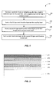
- FIG. 1 is a simplified flowchart of a method 10 for manufacturing a semiconductor device according to an embodiment of the present invention.
- the method 10 may include the following process steps:
- the second work function metal layer is richer in Ti atoms (Ti-rich), the Ti-rich second work function metal layer does not easily absorb oxygen from the atmosphere and blocks the oxygen absorption by the first work function metal layer, thereby reducing the level of oxidation of the first work function metal layer without affecting the device performance.
- the first N-type work function metal layer may include TiAl, TiCAl, TiNAl, TiSiAl, or combinations thereof.
- the second N-type work function metal layer may include Ti x Al y , Ti x C z Al y , Ti x N z Al y , Ti x Si z Al y , or combinations thereof, where x represents the ratio of atoms of Ti, y represents the ratio of atoms of Al, z represents the ratio of atoms of corresponding C, N, and Si, and x is greater than y. It should be understood that the above-described materials of the first and second N-type work function metal layers are preferred materials, and are not limited thereto.
- the oxidation level of the first N-type work function metal layer will be reduced as long as the ratio of the Ti and Al atoms of second N-type work function metal layer is greater than the ratio of the Ti and Al atoms of first N-type work function metal layer.
- those of skill in the art may select other suitable materials for the first N-type work function metal layer and the second N-type work function metal layer.
- the metal electrode layer may include W, Al, or other metal materials.
- the N-type work function metal layer in forming the gate stack structure, may be deposited in two steps, and the ratio of the Ti and Al atoms of the second N-type work function metal layer is greater than the ratio of the Ti and Al atoms of the first N-type work function metal layer, as to block the oxygen absorption in the atmosphere by the first N-type work function metal layer, thereby reducing the oxidation level of the N-type work function metal layer without affecting the device performance.
- the substrate structure in the above step 102 may be provided by a variety of processes, which will be described in detail below. The process of forming the substrate structure will now be described with reference to FIG. 2 through FIG. 4 .
- a substrate 201 is provided.
- An interface layer 202 is formed on the substrate 201, a high-k dielectric layer 203 is formed on the interface layer 202, a capping layer 204 is formed on the high-k dielectric layer 203, a barrier layer 205 is formed on the capping layer 204, and a P-type work function metal layer 206 is formed on the barrier layer 205.
- the substrate 201 may be a silicon substrate or other semiconductor substrate.
- the interface layer 202 may be a thermal oxide layer, which is configured to improve the interface properties between the high-k dielectric layer 203 and the substrate 201.
- the capping layer 204 may be TiN or TiSiN configured to block the diffusion of an aluminum element of a subsequently formed N-type work function layer into the high-k dielectric layer 203 to prevent adverse effects on the stability and other properties of the device.
- the barrier layer 205 may be TaN and used as an etch stop layer for a subsequently formed P-type work function metal layer.
- the P-type work function metal layer 206 may be Ti x N y (typically TiN) where x represents the ratio of atoms of Ti, y represents the ratio of atoms of N, TaN, TaC, and the like.
- FIG. 3 is a cross-sectional view illustrating a substrate structure 30 according to an embodiment of the present invention.
- the substrate structure 30 includes a substrate 201, an interface layer 202 on the substrate 201, a high-k dielectric layer 203 on the interface layer 202, and a capping layer 204 on the high-k dielectric layer 203. It is to be understood that, although an interface layer is shown between the substrate and the high-k dielectric layer, the interface layer is optional.
- the capping layer 204 may also be removed. Thereafter, a new capping layer 204 may be formed anew on the high-k dielectric layer 203 to form a substrate structure shown in FIG. 3 .
- the new capping layer can be formed in the same station as the deposition process of the first N-type work function metal layer.
- this process can prevent the capping layer 204 from absorbing oxygen from the environment, resulting in the oxidation of the N-type work function metal layer. Removing the capping layer, then forming a new capping layer in the same station as the deposition of the N-type work function metal layer can further reduce the oxidation of the N-type work function metal layer without affecting the device performance.
- the method for manufacturing a semiconductor device is suitable for planar devices as well as FinFET devices.
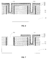
- FIG. 5 through FIG. 11 are cross-sectional views of intermediate stages of a method for manufacturing a semiconductor device according to embodiments of the present invention. It is noted that certain parts (e.g., source, drain, fin, etc.) are omitted to more clearly show the details of the gate stack structure.
- a method for manufacturing a semiconductor device will hereinafter be described in detail with reference to FIG. 5 through FIG. 11 .
- the substrate structure 50 includes an NMOS region having a first trench 5011 and a PMOS region having a second trench 5012.
- the substrate structure 50 may also include a shallow trench isolation (STI) structure (not shown).
- STI shallow trench isolation
- the first trench may include a first fin configured to be a channel region of an NMOS device
- the second trench may include a second fin configured to be a channel region of a PMOS device.
- the first and second trenches 5011, 5012 may be formed by the following process steps: forming a dummy gate structure including dummy gates and a dummy gate oxide layer in an interlayer dielectric layer 502 disposed on a substrate 501. Next, a planarization process is performed to expose the dummy gates disposed in the first trench 5011 and the second trench 5012. Thereafter, the dummy gates and the dummy gate oxide layer are removed to form the first gate trench 5011 and the second gate trench 5012. Spacer 503 is formed on sidewalls of the first and second trenches.
- the spacer 503 may be, for example, silicon oxide, silicon nitride, silicon oxynitride, and the like.
- source and drain regions of an NMOS device and a PMOS device may be formed on opposite sides of the first trench 5011 and the second trench 5012.
- the source and drain regions may be formed from an epitaxially grown SiC layer, the epitaxially grown SiC creates a tensile stress in the channel region of the NMOS device.
- the source and drain regions may be formed from an epitaxially grown SiGe layer, the epitaxially grown SiGe creates a compression stress in the channel region of the PMOS device.
- a high-k dielectric layer 601 is deposited on the bottom and sidewalls of the first trench 5011 and the second trench 5012, a capping layer 602 is deposited on the high-k dielectric layer 601, a barrier layer 603 is deposited on the capping layer 602, and a P-type work function metal layer 604 is deposited on the barrier layer 603.
- the bottom of the first and second trenches is the substrate.
- the bottom of the first and second trenches includes the surface and side surfaces of the fin.
- a high-k dielectric layer 601, a capping layer 602, a barrier layer 603, and a P-type work function layer 604 may be sequentially deposited in the first and second trenches 5011, 5012 by atomic layer deposition (ALD), chemical vapor deposition (CVD), or physical vapor deposition (PVD) process.
- ALD atomic layer deposition
- CVD chemical vapor deposition
- PVD physical vapor deposition
- an interface layer may be formed on the bottom and sidewalls of the first and second trenches 5011, 5012 prior to depositing the high-k dielectric layer 601.
- the interface layer may be a thermal oxide layer to improve the interface properties between the high-k dielectric layer and the substrate.
- the high-k dielectric layer may include, but not limited to, hafnium oxide, aluminum oxide, tantalum oxide, titanium oxide, zirconium oxide, or the like.
- a portion of the P-type work function metal layer 604, a portion of the barrier layer 603, and a portion of the capping layer 602 are removed from the bottom and sidewalls of the first trench 5011.
- a patterned photo resist is formed on the P-type work function metal layer 604 covering the PMOS region while exposing the NMOS region.
- a dry or wet etching process is performed to remove a portion of the P-type work function metal layer disposed in the NMOS region using the patterned photo resist as a mask and the barrier layer 603 as an etch stop layer. Thereafter, the portion of the barrier layer 603 and the portion of the capping layer 602 disposed in the NMOS region are removed.
- a new capping layer 602' is deposited on the high-k dielectric layer of the first trench 5011 and on the P-type work function metal layer 604 of the second trench 5012.
- a first N-type work function metal layer 901 is deposited on the new capping layer 602', and a second N-type work function metal layer 902 is deposited on the first N-type work function metal layer 901.
- the second N-type work function metal layer 902 has a ratio of the Ti and Al atoms (alternatively referred to as Ti/Al atomic ratio) greater than the ratio of the Ti and Al atoms of the first N-type work function metal layer 901.
- N-type work function metal layer(s) in the PMOS region may also be removed by additional process steps.
- a metal electrode layer 1001 is deposited on the second N-type work function metal layer 902, the metal electrode layer 1001 may be, for example, W, Al or other metal material.
- an adhesion layer e.g., TiN, Ti or a stacked structure including a combination of TiN and Ti may be deposited on the second N-type work function metal layer 902 to increase the bonding between the metal electrode layer and the second N-type work function metal layer.
- a planarization process is performed on the metal electrode layer to expose a surface of the interlayer dielectric layer 502, thereby forming a metal gate 1011 in the NMOS region and a metal gate 1021 in the PMOS region.
- the above-described process steps provide a method for manufacturing a gate stack structure, an NMOS device including the gate stack structure, a PMOS device, and a semiconductor device including the gate stack structure.
- the semiconductor device includes an NMOS device and a PMOS device.
- FIG. 11 is a cross-sectional view illustrating gate stack structures 11n and 11p and a semiconductor device 11 including the gate stack structures according to some embodiments of the present invention.
- the gate stack structure 11n in the NMOS region includes a substrate 501, a high-k dielectric layer 601 on the substrate 501, a capping layer 602' on the high-k dielectric layer, a first N-type work function metal layer 901 on the capping layer 602', a second N-type work function metal layer 902 on the first N-type work function metal layer 901, and a metal electrode layer 1011 on the second N-type work function metal layer 902.
- the Ti/Al atomic ratio of the second N-type work function metal layer 902 is greater than the Ti/Al atomic ratio of the first N-type work function metal layer 901.
- the gate stack structure 11p in the PMOS region includes the substrate 501, the high-k dielectric layer 601 on the substrate 501, a capping layer 602 on the high-k dielectric layer 601, a barrier layer 603 on the capping layer 602, a P-type work function layer 604 on the barrier layer 603, the capping layer 602' on the P-type work function layer 604, the first N-type work function metal layer 901 on the capping layer 602', the second N-type work function metal layer 902 on the first N-type work function metal layer 901, and the metal electrode layer 1011 on the second N-type work function metal layer 902.
- the Ti/Al atomic ratio of the second N-type work function metal layer 902 is greater than the Ti/Al atomic ratio of the first N-type work function metal layer 901.
- the gate stack structure may also include an interface layer disposed between the substrate 501 and the high-k dielectric layer 604, such as a thermal oxide layer.
- the gate stack structure may also include an adhesion layer disposed between the second N-type work function metal layer 902 and the metal electrode layer 1011, such as TiN, Ti, or a stacked structure including a combination of TiN and Ti.
- the capping layer 602' may include TiN or TiSiN.
- the first N-type work function metal layer 901 may include TiAl, TiCAl, TiNAl, TiSiAl, or any combinations thereof.
- the second N-type work function metal layer 902 may include Ti x Al y , Ti x C z Al y , Ti x N z Al y , Ti x Si z Al y , or any combinations thereof, where x represents the ratio of atoms of Ti, y represents the ratio of atoms of Al, and x is greater than y.
- the capping layer 602' and the first N-type work function metal layer 901 are formed in the same station.
- Embodiments of the present invention also provide an NMOS device that include the above-described gate stack structure 11n, a source, a drain, and others.
- Embodiments of the present invention also provide a semiconductor device including the above-described NMOS device having the above-described gate stack structure 11n and a PMOS device having the above-described gate stack structure 11p, a source, a drain, and others.
- the gate stack structures 11n and 11p may be formed in respective first and second trenches 5011 and 5012.
- the first and second trenches 5011 and 5012 may include respective first and second fins (not shown).
- the gate stacks 11n and 11p may be formed on a top surface and side surfaces of the fins.
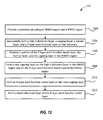
- FIG. 12 is a simplified flowchart of a method 120 for manufacturing a semiconductor device according to an embodiment of the present invention.
- the method 120 may include the following process steps:
- the capping layer is first removed, a new capping layer is then formed in the same station used for forming the first N-type work function metal layer, so that the oxygen absorption by the capping layer can be minimized or avoided, that will reduce or prevent, in turn, the oxidation of the N-type work function metal layer.
- the thus formed NMOS device has a stable work function and a threshold voltage.
Landscapes
- Metal-Oxide And Bipolar Metal-Oxide Semiconductor Integrated Circuits (AREA)
- Insulated Gate Type Field-Effect Transistor (AREA)
- Engineering & Computer Science (AREA)
- Electrodes Of Semiconductors (AREA)
- Manufacturing & Machinery (AREA)
- Chemical & Material Sciences (AREA)
- Composite Materials (AREA)
- Materials Engineering (AREA)
Applications Claiming Priority (1)
| Application Number | Priority Date | Filing Date | Title |
|---|---|---|---|
| CN201510674607.2A CN106601605B (zh) | 2015-10-19 | 2015-10-19 | 栅极堆叠结构、nmos器件、半导体装置及其制造方法 |
Publications (2)
| Publication Number | Publication Date |
|---|---|
| EP3159929A2 true EP3159929A2 (de) | 2017-04-26 |
| EP3159929A3 EP3159929A3 (de) | 2017-08-02 |
Family
ID=57178254
Family Applications (1)
| Application Number | Title | Priority Date | Filing Date |
|---|---|---|---|
| EP16193617.4A Withdrawn EP3159929A3 (de) | 2015-10-19 | 2016-10-13 | Verfahren und vorrichtung für metallgatestapel |
Country Status (3)
| Country | Link |
|---|---|
| US (1) | US10211309B2 (de) |
| EP (1) | EP3159929A3 (de) |
| CN (1) | CN106601605B (de) |
Cited By (1)
| Publication number | Priority date | Publication date | Assignee | Title |
|---|---|---|---|---|
| US10211309B2 (en) | 2015-10-19 | 2019-02-19 | Semiconductor Manufacturing International (Beijing) Corporation | Method and device for metal gate stacks |
Families Citing this family (14)
| Publication number | Priority date | Publication date | Assignee | Title |
|---|---|---|---|---|
| US10103147B1 (en) | 2017-05-01 | 2018-10-16 | International Business Machines Corporation | Vertical transport transistors with equal gate stack thicknesses |
| TWI730119B (zh) * | 2017-06-09 | 2021-06-11 | 聯華電子股份有限公司 | 具有金屬閘極之半導體元件之製作方法 |
| CN109950312B (zh) * | 2017-12-21 | 2022-03-18 | 中芯国际集成电路制造(上海)有限公司 | 半导体器件及其形成方法 |
| CN110534419B (zh) * | 2018-05-23 | 2022-04-08 | 中芯国际集成电路制造(上海)有限公司 | 一种半导体器件及其制造方法 |
| CN108777261A (zh) * | 2018-06-07 | 2018-11-09 | 上海华力集成电路制造有限公司 | 一种晶体管的栅极结构及其制造方法 |
| US11127857B2 (en) * | 2019-04-12 | 2021-09-21 | Taiwan Semiconductor Manufacturing Company, Ltd. | Semiconductor device and method of manufacture |
| US11056395B2 (en) * | 2019-08-23 | 2021-07-06 | Taiwan Semiconductor Manufacturing Company, Ltd. | Transistor metal gate and method of manufacture |
| US11183431B2 (en) * | 2019-09-05 | 2021-11-23 | Taiwan Semiconductor Manufacturing Co., Ltd. | Method of manufacturing semiconductor devices and semiconductor devices |
| US11430698B2 (en) | 2020-05-19 | 2022-08-30 | Taiwan Semiconductor Manufacturing Co., Ltd. | In-situ formation of metal gate modulators |
| US11437280B2 (en) * | 2020-06-12 | 2022-09-06 | Taiwan Semiconductor Manufacturing Co., Ltd. | Semiconductor device and method of manufacture |
| US11508826B2 (en) * | 2020-07-16 | 2022-11-22 | Taiwan Semiconductor Manufacturing Co., Ltd. | Composite work function layer formation using same work function material |
| CN114695538A (zh) * | 2022-02-21 | 2022-07-01 | 上海华力集成电路制造有限公司 | 具有hkmg的mos晶体管及其制造方法 |
| CN117954480A (zh) * | 2022-10-27 | 2024-04-30 | 华为技术有限公司 | 晶体管、集成电路及制备方法、电子设备 |
| US12490497B2 (en) * | 2022-12-29 | 2025-12-02 | Taiwan Semiconductor Manufacturing Company, Ltd. | Metal gate patterning |
Family Cites Families (28)
| Publication number | Priority date | Publication date | Assignee | Title |
|---|---|---|---|---|
| KR100613392B1 (ko) * | 2004-12-23 | 2006-08-17 | 동부일렉트로닉스 주식회사 | 자기 정렬 콘택홀 형성 방법 |
| US7109079B2 (en) | 2005-01-26 | 2006-09-19 | Freescale Semiconductor, Inc. | Metal gate transistor CMOS process and method for making |
| KR101358854B1 (ko) | 2007-09-06 | 2014-02-06 | 삼성전자주식회사 | 반도체 소자 및 상기 반도체 소자의 금속 게이트 형성 방법 |
| US8003507B2 (en) | 2008-08-18 | 2011-08-23 | Taiwan Semiconductor Manufacturing Company, Ltd. | Method of integrating high-K/metal gate in CMOS process flow |
| US7927943B2 (en) * | 2008-09-12 | 2011-04-19 | Taiwan Semiconductor Manufacturing Company, Ltd. | Method for tuning a work function of high-k metal gate devices |
| US8129280B2 (en) * | 2009-07-24 | 2012-03-06 | Applied Materials, Inc. | Substrate device having a tuned work function and methods of forming thereof |
| US8232154B2 (en) | 2009-09-21 | 2012-07-31 | United Microelectronics Corp. | Method for fabricating semiconductor device |
| US8704280B2 (en) | 2011-09-22 | 2014-04-22 | Taiwan Semiconductor Manufacturing Company, Ltd. | Semiconductor device with strained channels induced by high-k capping metal layers |
| US8963257B2 (en) * | 2011-11-10 | 2015-02-24 | Taiwan Semiconductor Manufacturing Company, Ltd. | Fin field effect transistors and methods for fabricating the same |
| US8546212B2 (en) * | 2011-12-21 | 2013-10-01 | United Microelectronics Corp. | Semiconductor device and fabricating method thereof |
| US8987080B2 (en) | 2012-04-26 | 2015-03-24 | Applied Materials, Inc. | Methods for manufacturing metal gates |
| KR20130127257A (ko) * | 2012-05-14 | 2013-11-22 | 삼성전자주식회사 | 반도체 장치 및 그 제조 방법 |
| KR101913434B1 (ko) | 2012-06-29 | 2018-10-30 | 에스케이하이닉스 주식회사 | 반도체 소자 및 그 제조 방법 |
| US8659077B1 (en) | 2012-09-13 | 2014-02-25 | International Business Machines Corporation | Multi-layer work function metal replacement gate |
| US8803254B2 (en) * | 2012-11-28 | 2014-08-12 | Globalfoundries Inc. | Methods of forming replacement gate structures for NFET semiconductor devices and devices having such gate structures |
| US9397217B2 (en) * | 2012-12-28 | 2016-07-19 | Taiwan Semiconductor Manufacturing Company, Ltd. | Contact structure of non-planar semiconductor device |
| US9129985B2 (en) * | 2013-03-05 | 2015-09-08 | United Microelectronics Corp. | Semiconductor device having metal gate and manufacturing method thereof |
| CN104253029B (zh) * | 2013-06-26 | 2017-11-28 | 中芯国际集成电路制造(上海)有限公司 | 晶体管的形成方法 |
| US9024392B2 (en) * | 2013-07-03 | 2015-05-05 | Taiwan Semiconductor Manufacturing Co., Ltd. | Multi-port SRAM manufacturing |
| KR102055379B1 (ko) | 2013-08-08 | 2019-12-13 | 삼성전자 주식회사 | 트라이-게이트를 포함하는 반도체 소자 및 그 제조 방법 |
| US9384984B2 (en) * | 2013-09-03 | 2016-07-05 | United Microelectronics Corp. | Semiconductor structure and method of forming the same |
| US9105720B2 (en) * | 2013-09-11 | 2015-08-11 | United Microelectronics Corp. | Semiconductor device having metal gate and manufacturing method thereof |
| US9196546B2 (en) * | 2013-09-13 | 2015-11-24 | United Microelectronics Corp. | Metal gate transistor |
| US9576952B2 (en) | 2014-02-25 | 2017-02-21 | Globalfoundries Inc. | Integrated circuits with varying gate structures and fabrication methods |
| US9236261B2 (en) * | 2014-04-01 | 2016-01-12 | Globalfoundries Inc. | Deposition of titanium-aluminum layers |
| US9418856B2 (en) * | 2014-11-06 | 2016-08-16 | Samsung Electronics Co., Ltd. | Methods of forming titanium-aluminum layers for gate electrodes and related semiconductor devices |
| TWI635535B (zh) * | 2015-03-10 | 2018-09-11 | 聯華電子股份有限公司 | 具有不同臨界電壓的金屬閘極的半導體製程及半導體結構 |
| CN106601605B (zh) | 2015-10-19 | 2020-02-28 | 中芯国际集成电路制造(北京)有限公司 | 栅极堆叠结构、nmos器件、半导体装置及其制造方法 |
-
2015
- 2015-10-19 CN CN201510674607.2A patent/CN106601605B/zh active Active
-
2016
- 2016-09-21 US US15/272,197 patent/US10211309B2/en active Active
- 2016-10-13 EP EP16193617.4A patent/EP3159929A3/de not_active Withdrawn
Non-Patent Citations (1)
| Title |
|---|
| None |
Cited By (1)
| Publication number | Priority date | Publication date | Assignee | Title |
|---|---|---|---|---|
| US10211309B2 (en) | 2015-10-19 | 2019-02-19 | Semiconductor Manufacturing International (Beijing) Corporation | Method and device for metal gate stacks |
Also Published As
| Publication number | Publication date |
|---|---|
| CN106601605B (zh) | 2020-02-28 |
| US10211309B2 (en) | 2019-02-19 |
| CN106601605A (zh) | 2017-04-26 |
| US20170110553A1 (en) | 2017-04-20 |
| EP3159929A3 (de) | 2017-08-02 |
Similar Documents
| Publication | Publication Date | Title |
|---|---|---|
| US10211309B2 (en) | Method and device for metal gate stacks | |
| CN101661883B (zh) | 半导体元件的制造方法 | |
| CN112447600A (zh) | 半导体装置的形成方法 | |
| US9685533B1 (en) | Transistor with SiCN/SiOCN mulitlayer spacer | |
| US10692779B2 (en) | Method and structure for CMOS metal gate stack | |
| CN108431953A (zh) | 垂直晶体管制造和器件 | |
| CN106298540A (zh) | 具有脱氧栅极堆叠件的多栅极场效应晶体管 | |
| US20200052116A1 (en) | Semiconductor device | |
| US8324118B2 (en) | Manufacturing method of metal gate structure | |
| US8921171B2 (en) | Method for forming gate structure, method for forming semiconductor device, and semiconductor device | |
| US9093477B1 (en) | Implantation processing step for a recess in finFET | |
| US9640660B2 (en) | Asymmetrical FinFET structure and method of manufacturing same | |
| EP3316289A2 (de) | Verfahren zur verbesserung der high-k-qualität | |
| TWI555067B (zh) | 積體電路裝置及其製造方法 | |
| US10367058B2 (en) | Channel stop imp for the FinFET device | |
| KR102311437B1 (ko) | 삽입 층을 구비한 반도체 구조체 및 이를 제조하는 방법 | |
| US20140124835A1 (en) | Semiconductor structure | |
| US8058121B2 (en) | Method for fabricating semiconductor device, method for fabricating bipolar-CMOS-DMOS | |
| US20140015062A1 (en) | Method for Forming Gate Structure, Method for Forming Semiconductor Device, and Semiconductor Device | |
| KR102394925B1 (ko) | 반도체 장치 및 이의 제조 방법 | |
| US12148619B2 (en) | Manufacturing method for semiconductor structure, and semiconductor structure | |
| CN118486590A (zh) | 半导体元件 | |
| CN108257915A (zh) | 一种半导体器件的制造方法 | |
| CN106298542A (zh) | 一种mosfet结构及其制造方法 |
Legal Events
| Date | Code | Title | Description |
|---|---|---|---|
| PUAI | Public reference made under article 153(3) epc to a published international application that has entered the european phase |
Free format text: ORIGINAL CODE: 0009012 |
|
| STAA | Information on the status of an ep patent application or granted ep patent |
Free format text: STATUS: THE APPLICATION HAS BEEN PUBLISHED |
|
| AK | Designated contracting states |
Kind code of ref document: A2 Designated state(s): AL AT BE BG CH CY CZ DE DK EE ES FI FR GB GR HR HU IE IS IT LI LT LU LV MC MK MT NL NO PL PT RO RS SE SI SK SM TR |
|
| AX | Request for extension of the european patent |
Extension state: BA ME |
|
| RAP1 | Party data changed (applicant data changed or rights of an application transferred) |
Owner name: SEMICONDUCTOR MANUFACTURING INTERNATIONAL CORPORAT |
|
| PUAL | Search report despatched |
Free format text: ORIGINAL CODE: 0009013 |
|
| AK | Designated contracting states |
Kind code of ref document: A3 Designated state(s): AL AT BE BG CH CY CZ DE DK EE ES FI FR GB GR HR HU IE IS IT LI LT LU LV MC MK MT NL NO PL PT RO RS SE SI SK SM TR |
|
| AX | Request for extension of the european patent |
Extension state: BA ME |
|
| RIC1 | Information provided on ipc code assigned before grant |
Ipc: H01L 21/8238 20060101AFI20170627BHEP Ipc: H01L 29/78 20060101ALI20170627BHEP Ipc: H01L 29/66 20060101ALI20170627BHEP |
|
| STAA | Information on the status of an ep patent application or granted ep patent |
Free format text: STATUS: REQUEST FOR EXAMINATION WAS MADE |
|
| 17P | Request for examination filed |
Effective date: 20180130 |
|
| RBV | Designated contracting states (corrected) |
Designated state(s): AL AT BE BG CH CY CZ DE DK EE ES FI FR GB GR HR HU IE IS IT LI LT LU LV MC MK MT NL NO PL PT RO RS SE SI SK SM TR |
|
| RIN1 | Information on inventor provided before grant (corrected) |
Inventor name: ZHOU, FEI |
|
| RAP1 | Party data changed (applicant data changed or rights of an application transferred) |
Owner name: SEMICONDUCTOR MANUFACTURING INTERNATIONAL (BEIJING Owner name: SEMICONDUCTOR MANUFACTURING INTERNATIONAL (SHANGHA |
|
| STAA | Information on the status of an ep patent application or granted ep patent |
Free format text: STATUS: EXAMINATION IS IN PROGRESS |
|
| 17Q | First examination report despatched |
Effective date: 20200519 |
|
| STAA | Information on the status of an ep patent application or granted ep patent |
Free format text: STATUS: THE APPLICATION IS DEEMED TO BE WITHDRAWN |
|
| 18D | Application deemed to be withdrawn |
Effective date: 20200930 |