EP3159945A2 - Anordnung und montage von solarzellen auf raumfahrzeugen oder satelliten - Google Patents
Anordnung und montage von solarzellen auf raumfahrzeugen oder satelliten Download PDFInfo
- Publication number
- EP3159945A2 EP3159945A2 EP16194199.2A EP16194199A EP3159945A2 EP 3159945 A2 EP3159945 A2 EP 3159945A2 EP 16194199 A EP16194199 A EP 16194199A EP 3159945 A2 EP3159945 A2 EP 3159945A2
- Authority
- EP
- European Patent Office
- Prior art keywords
- psa
- solar cell
- flexible support
- sensitive adhesive
- regions
- Prior art date
- Legal status (The legal status is an assumption and is not a legal conclusion. Google has not performed a legal analysis and makes no representation as to the accuracy of the status listed.)
- Pending
Links
Images





Classifications
-
- H—ELECTRICITY
- H10—SEMICONDUCTOR DEVICES; ELECTRIC SOLID-STATE DEVICES NOT OTHERWISE PROVIDED FOR
- H10F—INORGANIC SEMICONDUCTOR DEVICES SENSITIVE TO INFRARED RADIATION, LIGHT, ELECTROMAGNETIC RADIATION OF SHORTER WAVELENGTH OR CORPUSCULAR RADIATION
- H10F71/00—Manufacture or treatment of devices covered by this subclass
- H10F71/127—The active layers comprising only Group III-V materials, e.g. GaAs or InP
-
- B—PERFORMING OPERATIONS; TRANSPORTING
- B64—AIRCRAFT; AVIATION; COSMONAUTICS
- B64G—COSMONAUTICS; VEHICLES OR EQUIPMENT THEREFOR
- B64G1/00—Cosmonautic vehicles
- B64G1/22—Parts of, or equipment specially adapted for fitting in or to, cosmonautic vehicles
- B64G1/42—Arrangements or adaptations of power supply systems
- B64G1/44—Arrangements or adaptations of power supply systems using radiation, e.g. deployable solar arrays
- B64G1/443—Photovoltaic cell arrays
-
- H—ELECTRICITY
- H02—GENERATION; CONVERSION OR DISTRIBUTION OF ELECTRIC POWER
- H02S—GENERATION OF ELECTRIC POWER BY CONVERSION OF INFRARED RADIATION, VISIBLE LIGHT OR ULTRAVIOLET LIGHT, e.g. USING PHOTOVOLTAIC [PV] MODULES
- H02S30/00—Structural details of PV modules other than those related to light conversion
- H02S30/20—Collapsible or foldable PV modules
-
- H—ELECTRICITY
- H10—SEMICONDUCTOR DEVICES; ELECTRIC SOLID-STATE DEVICES NOT OTHERWISE PROVIDED FOR
- H10F—INORGANIC SEMICONDUCTOR DEVICES SENSITIVE TO INFRARED RADIATION, LIGHT, ELECTROMAGNETIC RADIATION OF SHORTER WAVELENGTH OR CORPUSCULAR RADIATION
- H10F10/00—Individual photovoltaic cells, e.g. solar cells
- H10F10/10—Individual photovoltaic cells, e.g. solar cells having potential barriers
- H10F10/14—Photovoltaic cells having only PN homojunction potential barriers
- H10F10/142—Photovoltaic cells having only PN homojunction potential barriers comprising multiple PN homojunctions, e.g. tandem cells
-
- H—ELECTRICITY
- H10—SEMICONDUCTOR DEVICES; ELECTRIC SOLID-STATE DEVICES NOT OTHERWISE PROVIDED FOR
- H10F—INORGANIC SEMICONDUCTOR DEVICES SENSITIVE TO INFRARED RADIATION, LIGHT, ELECTROMAGNETIC RADIATION OF SHORTER WAVELENGTH OR CORPUSCULAR RADIATION
- H10F19/00—Integrated devices, or assemblies of multiple devices, comprising at least one photovoltaic cell covered by group H10F10/00, e.g. photovoltaic modules
- H10F19/90—Structures for connecting between photovoltaic cells, e.g. interconnections or insulating spacers
- H10F19/902—Structures for connecting between photovoltaic cells, e.g. interconnections or insulating spacers for series or parallel connection of photovoltaic cells
-
- Y—GENERAL TAGGING OF NEW TECHNOLOGICAL DEVELOPMENTS; GENERAL TAGGING OF CROSS-SECTIONAL TECHNOLOGIES SPANNING OVER SEVERAL SECTIONS OF THE IPC; TECHNICAL SUBJECTS COVERED BY FORMER USPC CROSS-REFERENCE ART COLLECTIONS [XRACs] AND DIGESTS
- Y02—TECHNOLOGIES OR APPLICATIONS FOR MITIGATION OR ADAPTATION AGAINST CLIMATE CHANGE
- Y02E—REDUCTION OF GREENHOUSE GAS [GHG] EMISSIONS, RELATED TO ENERGY GENERATION, TRANSMISSION OR DISTRIBUTION
- Y02E10/00—Energy generation through renewable energy sources
- Y02E10/50—Photovoltaic [PV] energy
- Y02E10/544—Solar cells from Group III-V materials
-
- Y—GENERAL TAGGING OF NEW TECHNOLOGICAL DEVELOPMENTS; GENERAL TAGGING OF CROSS-SECTIONAL TECHNOLOGIES SPANNING OVER SEVERAL SECTIONS OF THE IPC; TECHNICAL SUBJECTS COVERED BY FORMER USPC CROSS-REFERENCE ART COLLECTIONS [XRACs] AND DIGESTS
- Y02—TECHNOLOGIES OR APPLICATIONS FOR MITIGATION OR ADAPTATION AGAINST CLIMATE CHANGE
- Y02P—CLIMATE CHANGE MITIGATION TECHNOLOGIES IN THE PRODUCTION OR PROCESSING OF GOODS
- Y02P70/00—Climate change mitigation technologies in the production process for final industrial or consumer products
- Y02P70/50—Manufacturing or production processes characterised by the final manufactured product
Definitions
- the present disclosure relates to the field of photovoltaic solar arrays, and more particularly to fabrication processes utilizing, for example, multijunction solar cells based on III-V semiconductor compounds fabricated into interconnected Cell-Interconnect-Cover Glass (CIC) assemblies and mounted on a support or substrate using automated processes.
- CIC Cell-Interconnect-Cover Glass
- III-V compound semiconductor multijunction solar cells Solar power from photovoltaic cells, also called solar cells, has been predominantly provided by silicon semiconductor technology.
- high-volume manufacturing of III-V compound semiconductor multijunction solar cells for space applications has accelerated the development of such technology not only for use in space but also for terrestrial solar power applications.
- III-V compound semiconductor multijunction devices have greater energy conversion efficiencies and generally more radiation resistance, although they tend to be more complex to manufacture.
- Typical commercial III-V compound semiconductor multijunction solar cells have energy efficiencies that exceed 27% under one sun, air mass 0 (AM0), illumination, whereas even the most efficient silicon technologies generally reach only about 18% efficiency under comparable conditions.
- III-V compound semiconductor solar cells compared to silicon solar cells is in part based on the ability to achieve spectral splitting of the incident radiation through the use of a plurality of photovoltaic regions with different band gap energies, and accumulating the current from each of the regions.
- III-V compound semiconductor solar cells are fabricated on a semiconductor wafer in vertical, multijunction structures.
- the individual solar cells or wafers are then disposed in horizontal arrays, with the individual solar cells connected together in an electrical series circuit.
- the shape and structure of an array, as well as the number of cells it contains, are determined in part by the desired output voltage and current.
- the size, mass and cost of a satellite power system are dependent on the power and energy conversion efficiency of the solar cells used. Putting it another way, the size of the payload and the availability of on-board services are proportional to the amount of power provided.
- the power-to-weight ratio of a solar cell becomes increasingly more important, and there is increasing interest in lighter weight, "thin film” type solar cells having both high efficiency and low mass.
- a conventional space solar array panel may include a panel or support, solar cell assemblies disposed on the support, interconnection components for connecting the solar cell assemblies, and bypass diodes and blocking diodes also connected to the solar cells.
- CICs Cell-Interconnect-Cover Glass
- these CICs are connected in series to form strings, generally in a substantially manual manner, including welding or soldering steps. Then, these strings are applied to a panel or substrate and interconnected, in a process that includes the application of adhesive, wiring, and other assembly steps.
- the present disclosure provides improved methods of manufacturing and assembling photovoltaic solar arrays that can result in decreases in cost, greater compactness, and increases in performance.
- the present disclosure provides solar cell array modules, and methods of making and using solar cell array modules, having discrete predefined pressure sensitive adhesive (PSA) regions thereon.
- the solar cell array modules may be conveniently mounted on a space vehicle or satellite with the discrete predefined PSA regions.
- the present disclosure provides a method of fabricating a solar cell array module comprising: providing a release carrier having a sequence of pressure sensitive adhesive (PSA) patches on a first side of the release carrier; contacting the PSA patches on the first side of the release carrier with a first side of a flexible support and under conditions effective to transfer the PSA patches to the first side of the flexible support using an automated process to form discrete predefined PSA regions on the first side of the flexible support; and contacting the PSA regions on the first side of the flexible support with a first side of a release carrier having a sequence of solar cell assemblies thereon under conditions effective to transfer the solar cell assemblies to the PSA regions on the first side of the flexible support using an automated process to attach the sequence of solar cell assemblies to the first side of the flexible support using the PSA regions to prepare a patterned solar cell array.
- the method further includes providing a pressure sensitive adhesive on the second side of the flexible support.
- the release carrier having the sequence of pressure sensitive adhesive (PSA) patches on the first side of the release carrier is provided on a cassette or spool.
- PSA pressure sensitive adhesive
- conditions effective to transfer the PSA patches to the first side of the flexible support comprise: unwinding the release carrier having the sequence of pressure sensitive adhesive (PSA) patches on the first side of the release carrier from the cassette or spool and passing the release carrier through a first automated assembly device in a first direction, wherein the first automated assembly device has two rollers rotating in the same direction; and passing the flexible support through the first automated assembly device in a direction opposite the first direction in which the release carrier passes through the first automated assembly device; wherein the PSA patches on the first side of the release carrier are contacted with a first side of a flexible support and pressure from the two rollers is effective to transfer the PSA patches to the first side of the flexible support to form discrete predefined PSA regions on the first side of the flexible support.
- PSA pressure sensitive adhesive
- the release carrier having a sequence of solar cell assemblies on the first side thereof is provided on a cassette or spool.
- conditions effective to transfer the solar cell assemblies to the PSA regions on the first side of the flexible support comprise: unwinding the release carrier having the sequence of solar cell assemblies on the first side thereof from the cassette or spool and passing the release carrier through a second automated assembly device in a first direction, wherein the second automated assembly device has two rollers rotating in opposite directions; and passing the flexible support having a pattern of discrete predefined pressure sensitive adhesive (PSA) regions on a first side of the flexible support through the second automated assembly device in the same direction as the first direction in which the release carrier having the sequence of solar cell assemblies on the first side thereof passes through the second automated assembly device; wherein the solar cell assemblies on the first side of the release carrier are contacted with the first side of the flexible support having a pattern of discrete predefined pressure sensitive adhesive (PSA) regions, and pressure from the two rollers is effective to attach the sequence of solar cell assemblies to the PSA regions on the first side of the flexible support to prepare a patterned solar cell array.
- PSA pressure sensitive adhesive
- the pressure sensitive adhesive on the second side of the support is patterned. In some embodiments, the pattern of the pressure sensitive adhesive on the second side of the support are in the shape of and congruent to the shape of the surface of a space vehicle or satellite. In some embodiments, preparing the pattern of the pressure sensitive adhesive on the second side of the support is performed using an automated process.
- the present disclosure provides a method of fabricating a solar cell array module comprising: providing an aluminum honeycomb support with a carbon composite face sheet having an array of solar cell assemblies mounted on the face sheet; providing a pattern of discrete predefined pressure sensitive adhesive (PSA) regions on the side of the support opposite the face sheet; and providing a release liner adjacent the discrete predefined pressure sensitive adhesive (PSA) regions on the side of the support opposite the face sheet.
- PSA pressure sensitive adhesive
- the present disclosure provides a solar cell array module comprising: a support having an array of solar cells mounted on a first side of the support and a pattern of discrete predefined pressure sensitive adhesive (PSA) regions on a second side of the support; and a release liner adjacent the discrete predefined pressure sensitive adhesive (PSA) regions on the second side of the support.
- a solar cell array module comprising: a support having an array of solar cells mounted on a first side of the support and a pattern of discrete predefined pressure sensitive adhesive (PSA) regions on a second side of the support; and a release liner adjacent the discrete predefined pressure sensitive adhesive (PSA) regions on the second side of the support.
- PSA pressure sensitive adhesive
- the present disclosure provides a method of mounting a solar cell array module on a space vehicle or satellite comprising: providing a solar cell array module as described herein; removing the release liner; placing the discrete predefined pressure sensitive adhesive (PSA) regions of the solar cell array module adjacent a surface of the space vehicle; and applying pressure (e.g., manually or by an automated process).
- PSA pressure sensitive adhesive
- a plurality of solar cells are disposed closely adjacent to one another on each of the strips by a distance between 5 and 25 microns.
- each of the solar cells have a dimension in the range of 0.5 to 10 mm on a side.
- the support is a KAPTON® layer, that is, a polymide film layer.
- KAPTON® is a trademark of E.I. du Pont de Nemours and Company.
- the chemical name for KAPTON® is poly(4,4'-oxydiphenylene-pyromellitimide).
- Other polymide film sheets or layers may also be used.
- the support has a thickness of between 25 and 100 microns, or between 1 mil (25.4 ⁇ m) and 4 mil (101.6 ⁇ m).
- the metal layer is attached to the support layer in an adhesive-less manner, to limit outgassing when used in a space environment.
- a double-faced pressure-sensitive adhesive template or patch is positioned on the backside of the solar cell assembly.
- the support is mounted on a metallic honeycomb structure.
- the double-faced pressure-sensitive adhesive template or patch is shaped so that the shape matches and is congruent to that of the peripheral outline of the solar cell assembly.
- the double-faced pressure-sensitive adhesive template or patch and the polyimide film are bonded together by a co-curing process.
- the double-faced pressure-sensitive adhesive template or patch is covered at least partially with a release liner which is removed before making the bonding with the substrate.
- the release liner is at least partially patterned so that it matches the shape of the double-faced pressure-sensitive adhesive template or patch.
- the solar cell device and a substrate are automatically bonded together with at least one double-faced pressure adhesive patch, where the at least one double-faced pressure adhesive patch is at least partially positioned on backside of the solar cell device, in particular the interior of the solar cell device and / or at least partially positioned on the substrate before making the bonding connection.
- the at least one double-faced pressure sensitive adhesive patch is applied to the substrate, in particular a polymer film, more particular a polyimide film, the shape of the at least one double-faced pressure sensitive adhesive patch patterned to match the shape of the at least one solar cell device.
- the solar cell device is automatically positioned on the substrate so that its shape essentially matches the shape of at least one double-faced pressure sensitive adhesive patch.
- At least two solar cell devices are automatically interconnected using a pick and place process for positioning the interconnectors, followed by automatic parallel gap welding.
- the at least two solar cell devices are automatically electrically connected, in particular wire bonded together, the at least two solar cell devices having co-planar front-side electrical contacts.
- a single-layer pressure sensitive adhesive (PSA) film is used as a bonding adhesive to attach solar cells or solar cell assemblies to a solar panel.
- PSA pressure sensitive adhesive
- the PSA film may be a patterned or a continuous layer.
- the PSA film may be an acrylic or a silicone adhesive, or any other suitable material.
- the PSA film may have one or two release liners, or possibly no release liners.
- the substrate may be a rigid substrate, such as an aluminum honeycomb substrate with carbon composite face sheet, or it may be a flexible substrate, such as a polymide film.
- the PSA film may also be applied to the back of the solar cells or solar cell assemblies.
- a pressure sensitive adhesive (PSA) film is prepared as a single layer.
- the PSA film may be prepared onto a permanent flexible substrate, such as a polyimide, with a release liner or liners on the opposite side.
- a permanent flexible substrate such as a polyimide
- the PSA film is used to bond solar cells or solar cell assemblies to a substrate.
- the PSA film may be applied first to the substrate, and then the solar cells attached to the PSA film, or it may be applied first to the back of the solar cells, and then the solar cells with PSA film are applied to the substrate.
- the solar cells or solar cell assemblies may be applied directly to the PSA film.
- the PSA film may have continuous release liners that are removed in one step, or it may have a multiplicity of release liners that are removed individually.
- the PSA may be a silicone adhesive, an acrylic adhesive, or any other material that may be suitable for a PSA.
- the PSA may be a patterned layer, or it may be a continuous layer.
- the PSA may be patterned into the shape of solar cells.
- the assembly of polyimide-PSA-release liner is bonded directly to a solar panel substrate by co-curing the polyimide film to the face of the solar panel substrate.
- the solar panel substrate to which the polyimide is bonded may be an aluminum honeycomb substrate, and it may have a carbon composite or aluminum face sheet. It may be a rigid substrate, or it may be a flexible substrate.
- the substrate is ready to have the solar cells or solar cell assemblies bonded to it.
- the release liner is removed when it is time to bond the solar cells, which exposes the PSA, and the solar cells are bonded to the PSA and the substrate. Since the PSA thickness is precisely controlled during manufacturing, the bondline is uniform and there is less opportunity to entrap air than when a liquid adhesive is used.
- the present disclosure provides a space vehicle and its method of fabrication comprising: a payload disposed on or within the space vehicle; and a power source for the payload, including an array of solar cell assemblies mounted on a panel, each solar cell assembly being of the type described above.
- multijunction solar cells A variety of different features of multijunction solar cells are disclosed in the related applications noted above. Some, many or all of such features may be included in the structures and processes associated with the solar cells of the present disclosure. However, more particularly, the present disclosure is directed to several embodiments of mounting a plurality of solar cells to a support.
- the present disclosure may be adapted to multijunction solar cells as disclosed in related applications that may include three, four, five, or six subcells, with band gaps in the range of 1.8 to 2.2 eV (or higher) for the top subcell; 1.3 to 1.8 eV and 0.9 to 1.2 eV for the middle subcells; and 0.6 to 0.8 eV for the bottom subcell, respectively.
- the present disclosure provides a process for the design and fabrication of an array of covered-interconnect-cells or "CICs" using multijunction solar cells that improve manufacturing efficiency and/or performance. More specifically, the present disclosure intends to provide a relatively simple and reproducible technique that is suitable for use in a high volume production environment in which various semiconductor layers are deposited in an MOCVD reactor, and subsequent processing steps are defined and selected to minimize any physical damage to solar cell and the quality of the deposited layers, thereby ensuring a relatively high yield of operable solar cells meeting specifications at the conclusion of the fabrication processes.
- FIG. 1A is a top plan view of a wafer with two solar cells (cell 1 and cell 2) being implemented. Such solar cells may be referred to as "half-wafer" cells.
- FIG. 1B is a top plan view of a wafer with a single solar cell (cell 3) being implemented.
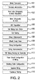
- FIG. 2 is a flowchart representing a method in accordance with an embodiment of the present disclosure.
- Certain embodiments of the invention can include one or more of the method steps of wafer fabrication (101), backside metallization (102), front side lithography and metal deposition (103), mesa lithography and etch (104), antireflective coating (ARC) deposition (105), cell dicing from the wafer (106), cell testing (107), attaching interconnects and configuring and attaching bypass diodes (108), attaching cover glass to form CIC (109), forming string configuration (110), forming string interconnections (111), CIC string bonding to substrate (112), panel circuit configuration and wiring (113), blocking diode configuration (114), terminal wiring (115), and functional testing (116).
- wafer fabrication 101
- backside metallization 102
- front side lithography and metal deposition 103
- mesa lithography and etch 104
- antireflective coating (ARC) deposition 105
- one or more of the above-recited method steps may be performed using an automated process.
- Solar cell configurations particularly suitable for assembly using automated processes include those that are described in U.S. Patent Application No. 14/592,519, filed January 8, 2015 ; 14/719,111, filed May 21, 2015 ; 14/729,412, filed June 3, 2015 ; and 14/729,422, filed June 3, 2015 , all of which are incorporated herein by reference in their entireties.
- One or more solar cells can be formed from a wafer using conventional techniques such as dicing or scribing.
- the size and shape of the solar cells can be varied as desired for particular applications as disclosed, for example, in U.S. Patent Application No. 14/592,519, filed January 8, 2015 , which is incorporated herein by reference in its entirety. Dicing or scribing of solar cells from a wafer is particularly amenable to automation using machine vision.
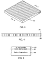
- FIG. 3 is a perspective view of a metallic honeycomb structure 200 which can be used for mounting a support.
- FIG. 4 is a cross-sectional view of an aluminum honeycomb substrate 200 with carbon composite face sheet 201 attached thereto.
- a double sided adhesive film can be positioned on the top surface of the face sheet, and the bottom surface of the adhesive film can be bonded to the top surface of the face sheet by, for example, co-curing.
- a plurality of layers of carbon composite sheets can be embedded in a matrix of cyanate ester adhesive. The polyimide can then be put on top and the whole stack co-cured.
- a sequence of solar cell assemblies can be positioned over the top surface of the adhesive film, and each of the sequence of solar cell assemblies can be sequentially bonded to a predefined region on the top surface of the adhesive film, for example, by automatic application of pressure and/or heat.
- the predefined region contains a pressure sensitive adhesive, and no adhesive is present on other regions of the top surface of the face sheet.
- FIG. 5 is a cross-sectional view of an aluminum honeycomb substrate 200 with carbon composite face sheet 201 attached to aluminum honeycomb substrate 200, and co-cured polyimide substrate 202 attached to carbon composite face sheet 201.
- FIG. 6 is a cross sectional view of an assembly for applying patterns of PSA patches to a polyimide sheet in an automated manner.
- a sequence of PSA patches 203e, 203f, 203g, 203h, 203i, ... are disposed on a first side of release carrier 204.
- the PSA patches 203e, 203f, 203g, 203h, 203i, ... are placed in contact with a first side of polyimide sheet 202.
- a second side of release carrier 204 is in contact with roller 205, and a second side of polyimide sheet 202 is in contact with roller 206.
- Rollers 205 and 206 are rotating in the same direction (i.e., both either clockwise or counter-clockwise), which causes release carrier 204 and polyimide sheet 202 to be transported between rollers 205 and 206 in opposite directions.
- release carrier 204 and polyimide sheet 202 pass through rollers 205 and 206, PSA patches 203e, 203f, 203g, 203h, 203i, ... each come in contact with the first side of polyimide sheet 202.
- Rollers 205 and 206 can exert sufficient pressure on polyimide sheet 202 and release liner 204 to cause each PSA patch to be automatically transferred from the first side of release liner 204 and sequentially positioned on the first side of polyimide film 202 as shown for PSA patches 203d, 203c, 203b, and 203a.
- FIG. 7 is a perspective view of substrate 200 having a pre-selected pattern of PSA templates or patches 203a, 203b, 203c, ... on pre-determined regions of the surface of polyimide face sheet 202 after attachment by the assembly of FIG. 6 .
- FIG. 8 is a perspective view of an array of solar cells 210a, 210b, 210c, ... mounted on the PSA templates or patches 203a, 203b, 203c, ... , respectively, as depicted in FIG. 7 .
- the array of solar cells 210a, 210b, 210c, ... can be mounted on the PSA templates or patches 203a, 203b, 203c, ... , respectively, by a wide variety of methods.
- the sequence of solar cell assemblies 210a, 210b, 210c, ... can be disposed on a release carrier, and each solar cell assembly 210a, 210b, 210c, ... can be detached from the release carrier as the solar cell assembly is bonded to a respective PSA template or patch 203a, 203b, 203c, ... in a predefined region of polyimide face sheet 202 of substrate 200.
- FIG. 9 is a cross sectional view of an automated assembly process for mounting the solar cell assemblies on patterns of PSA patches attached to a polyimide sheet.
- a sequence of solar cell assemblies 210d, 210e, 210f, 210g, ... are disposed on a first side of release carrier 204.
- the PSA patches 203a, 203b, 203c, 203d, 203e, 203f, ... disposed in predefined regions on a first side of polyimide sheet 202 are placed in contact with the sequence of solar cell assemblies 210d, 210e, 210f, 210g, ... disposed on a fist side of release carrier 204.
- a second side of release carrier 204 is in contact with roller 212, and a second side of polyimide sheet 202 is in contact with roller 211.
- Rollers 211 and 212 are rotating in the opposite directions (i.e., one clockwise and the other counter-clockwise), which causes release carrier 204 and polyimide sheet 202 to be transported between rollers 211 and 212 in the same direction.
- PSA patches 203a, 203b, 203c, 203d, 203e, 203f, ... on polyimide sheet 202 each come in contact with solar cell assemblies 210d, 210e, 210f, 210g, ... disposed on release carrier 204.
- Rollers 211 and 212 can exert sufficient pressure on polyimide sheet 202 and release liner 204 to cause each solar assembly to be automatically transferred from the first side of release liner 204 and sequentially positioned on PSA patches 203a, 203b, 203c, 203d, 203e, 203f, ... on the first side of polyimide sheet 202 as shown for solar cell assemblies 210a, 210b, 210c, and 210d adhered to PSA patches 203a, 203b, 203c, and 203d, respectively, on pre-determined regions of the first side of polyimide sheet 202.
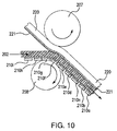
- FIG. 10 is a cross sectional view of an automated assembly process for applying the PSA 221/release liner 220 construction on the side of polyimide sheet 202 opposite solar cell assemblies 210a, 210b, 210c, 210d, 210e, 210f, 210g, 210h, 210i, ...
- PSA 221 may be a continuous layer adjacent release liner 220.
- PSA 221 may be a patterned layer adjacent release liner 220.
- the side of the polyimide sheet 202 having solar cell assemblies 210a, 210b, 210c, 210d, 210e, 210f, 210g, 210h, 210i, ... attached thereto is in contact with roller 208.
- rollers 207 and 208 are rotating in opposite directions (i.e., one clockwise and the other counter-clockwise), which causes polyimide sheet 202 and the release liner 220/PSA 221 construction to be transported between rollers 207 and 208 in the same direction.
- PSA 221 comes in contact with the side of polyimide sheet 202 opposite solar cell assemblies 210a, 210b, 210c, 210d, 210e, 210f, 210g, 210h, 210i, ...
- Rollers 207 and 208 can exert sufficient pressure on polyimide sheet 202 and the release liner 220/PSA 221 construction to adhere PSA 220 to polyimide sheet 202.
- the solar cell assemblies may have a substantially square or rectangular shape with a dimension (width and/or length) of about 100 ⁇ m to 3 cm, in some embodiments, 500 ⁇ m to 1 cm, in some embodiments, 1 mm to 5 mm.
- the solar cell may have an area of about 0.01 mm 2 to 9 cm 2 , in some embodiments, about 0.25 mm 2 to 1 cm 2 , in some embodiments, about 1 mm 2 to 25 mm 2 .
- the MIC (the module including an array of cells mounted on a sheet or a support) may have dimensions of about 25 mm by 25 mm to about 600 mm by 600 mm.
- the MIC may be about 50 mm by 50 mm to 300 mm by 300m.
- the MIC may be 100 mm by 100 mm to 200 mm by 200 mm.
- the module may have an area of about 600 mm 2 to 3600 cm 2 , in some embodiments about 25 cm 2 to 900 cm 2 , in some embodiments 100 cm 2 to 400 cm 2 .
- a solar cell wafer having a diameter of 100 mm or 150 mm and a surface area in the order of 80 cm 2 or 180 cm 2 can be used to produce a large amount of small solar cells, such as square or rectangular solar cells each having a surface area of less than 9 cm 2 , less than 1 cm 2 , less than 0.1 cm 2 or even less than 0.05 cm 2 or less than 0.01 cm 2 .
- substantially rectangular -such as square- solar cells can be obtained in which the sides are less than 30, 10, 5, 3, 2, 1 or even 0.5 mm long. Thereby, the amount of waste of wafer material can be substantially reduced, and at the same time a high fill factor can be obtained.
- FIG. 11 is a plan view illustrating dies 120 with relatively small areas being defined to be diced or cut out from a wafer 100 according an embodiment of the present disclosure.
- the solar cells 120 may each have an area as described above, for example, of about 0.1 mm 2 to about 100 mm 2 .
- the wasted area of the wafer 100 which cannot be used to fabricate solar cells 120 is significantly reduced compared to other known methods.
- the wafer utilization may be from 88% to 95%.
- solar cells 120 corresponding to a defective region of the wafer can easily be discarded so as not to impair the performance of the module produced from the solar cells.
- FIG. 12 is a top perspective view of a module with an array of solar cells 116, 117, ... , and 507 mounted on the surface of the first side of a support.
- a contact 207a of the first polarity type and two contacts 207b, 507b of the second polarity type of are shown in relation to two solar cells 117, 507.
- the solar cells can be conveniently be electrically connected using interconnects as described, for example, in U.S. Patent Application No. 14/833,755, filed August 24, 2015 .
- FIG. 13 is a perspective view of solar cell module 250 with polyimide sheet 202 having a pattern of PSA patches 221 a, 221 b, and 221 c on the side of polyimide sheet 202 opposite solar cells 203a, 203b, and 203c, which can be prepared, for example, as described for FIG. 10 .
- release liner 220 has been removed to reveal a pattern of PSA patches.
- Polyimide sheets having PSA and a release liner on the side of polyimide sheet opposite the solar cells can conveniently be used to attach the solar cell module to a space vehicle or satellite.
- the release liner can be removed and the solar cell module can be attached to the surface of the space vehicle or satellite by the application of pressure, either manually or automatically.
- CubeSats are a type of miniaturized space vehicles or satellites.
- a typical CubeSat is a 10 cm x 10 cm x 10 cm cube, thus having a volume of one liter.
- CubeSats can be attached to one another in strings or blocks to provide functionalities and capabilities that would not otherwise be practically available in a single CubeSat.
- one CubeSat can be used as a power source to supply power necessary for other attached CubeSats to perform their functions such as imaging, sensing, or communications.
- the solar cell modules described herein can be particularly advantageous for attaching to a CubeSat.
- the solar cell module can be attached directly to the surface of the CubeSat without a need for a frame (e.g., an aluminum frame).
- the solar cell modules can include a light weight flexible support (e.g., polyimide support) or a non-flexible support (egg shell support).
- the PSA on the polyimide sheets can be a continuous layer or a patterned layer designed for a particular application.
- FIG. 14 illustrates an exemplary perspective view of solar cell module 250 having a patterned PSA layer on polyimide sheet 202.
- the particular pattern 221 d for the PSA in FIG. 14 is designed to match the framework on the surface of a CubeSat 1000 as illustrated in FIG. 15 .
Landscapes
- Engineering & Computer Science (AREA)
- Life Sciences & Earth Sciences (AREA)
- Sustainable Development (AREA)
- Remote Sensing (AREA)
- Aviation & Aerospace Engineering (AREA)
- Photovoltaic Devices (AREA)
Applications Claiming Priority (2)
| Application Number | Priority Date | Filing Date | Title |
|---|---|---|---|
| US201562243243P | 2015-10-19 | 2015-10-19 | |
| US15/241,418 US10276742B2 (en) | 2015-07-09 | 2016-08-19 | Assembly and mounting of solar cells on space vehicles or satellites |
Publications (2)
| Publication Number | Publication Date |
|---|---|
| EP3159945A2 true EP3159945A2 (de) | 2017-04-26 |
| EP3159945A3 EP3159945A3 (de) | 2017-08-02 |
Family
ID=57137980
Family Applications (1)
| Application Number | Title | Priority Date | Filing Date |
|---|---|---|---|
| EP16194199.2A Pending EP3159945A3 (de) | 2015-10-19 | 2016-10-17 | Anordnung und montage von solarzellen auf raumfahrzeugen oder satelliten |
Country Status (2)
| Country | Link |
|---|---|
| EP (1) | EP3159945A3 (de) |
| DE (1) | DE102016012187A1 (de) |
Cited By (1)
| Publication number | Priority date | Publication date | Assignee | Title |
|---|---|---|---|---|
| WO2024089694A1 (en) * | 2022-10-27 | 2024-05-02 | Solarpaint Ltd. | Solar cell having integrated isolated electrical contacts |
Citations (4)
| Publication number | Priority date | Publication date | Assignee | Title |
|---|---|---|---|---|
| CN101436624A (zh) * | 2008-12-25 | 2009-05-20 | 上海交通大学 | 空间太阳电池基板表面贴装电池串的方法 |
| US20120103388A1 (en) * | 2010-10-29 | 2012-05-03 | Applied Materials, Inc. | Monolithic module assembly using back contact solar cells and metal ribbon |
| US9444004B1 (en) * | 2014-05-02 | 2016-09-13 | Deployable Space Systems, Inc. | System and method for producing modular photovoltaic panel assemblies for space solar arrays |
| US20170012160A1 (en) * | 2015-07-09 | 2017-01-12 | Solaero Technologies Corp. | Assembly and mounting of solar cells on space panels |
Family Cites Families (4)
| Publication number | Priority date | Publication date | Assignee | Title |
|---|---|---|---|---|
| US6555739B2 (en) * | 2001-09-10 | 2003-04-29 | Ekla-Tek, Llc | Photovoltaic array and method of manufacturing same |
| KR20120094039A (ko) * | 2009-11-18 | 2012-08-23 | 쓰리엠 이노베이티브 프로퍼티즈 컴파니 | 가요성 조립체, 및 그의 제조 및 사용 방법 |
| JP2012064821A (ja) * | 2010-09-17 | 2012-03-29 | Fuji Electric Co Ltd | 太陽電池モジュールおよびその製造方法 |
| DE102010062823A1 (de) * | 2010-12-10 | 2012-06-21 | Tesa Se | Klebmasse und Verfahren zur Kapselung einer elektronischen Anordnung |
-
2016
- 2016-10-11 DE DE102016012187.4A patent/DE102016012187A1/de active Pending
- 2016-10-17 EP EP16194199.2A patent/EP3159945A3/de active Pending
Patent Citations (4)
| Publication number | Priority date | Publication date | Assignee | Title |
|---|---|---|---|---|
| CN101436624A (zh) * | 2008-12-25 | 2009-05-20 | 上海交通大学 | 空间太阳电池基板表面贴装电池串的方法 |
| US20120103388A1 (en) * | 2010-10-29 | 2012-05-03 | Applied Materials, Inc. | Monolithic module assembly using back contact solar cells and metal ribbon |
| US9444004B1 (en) * | 2014-05-02 | 2016-09-13 | Deployable Space Systems, Inc. | System and method for producing modular photovoltaic panel assemblies for space solar arrays |
| US20170012160A1 (en) * | 2015-07-09 | 2017-01-12 | Solaero Technologies Corp. | Assembly and mounting of solar cells on space panels |
Non-Patent Citations (1)
| Title |
|---|
| ZHUANG FU ET AL: "Automatic coating and fastening robot of space solar module to solar panel substrate", ASSEMBLY AUTOMATION, EMERALD GROUP PUBLISHING LTD, GB, vol. 28, no. 4, 1 January 2008 (2008-01-01), pages 301 - 307, XP009531499, ISSN: 0144-5154, DOI: 10.1108/01445150810904459 * |
Cited By (1)
| Publication number | Priority date | Publication date | Assignee | Title |
|---|---|---|---|---|
| WO2024089694A1 (en) * | 2022-10-27 | 2024-05-02 | Solarpaint Ltd. | Solar cell having integrated isolated electrical contacts |
Also Published As
| Publication number | Publication date |
|---|---|
| EP3159945A3 (de) | 2017-08-02 |
| DE102016012187A1 (de) | 2017-04-20 |
Similar Documents
| Publication | Publication Date | Title |
|---|---|---|
| US12119424B2 (en) | Automated assembly and mounting of solar cells on a honeycomb support | |
| US11817523B2 (en) | Automated assembly and mounting of solar cells on space panels | |
| US9608156B2 (en) | Assembly and mounting of solar cells on space panels | |
| US6555739B2 (en) | Photovoltaic array and method of manufacturing same | |
| US20220136320A1 (en) | Automated interconnection and mounting of solar cells on cell-interconnect-cover glass (cic) assemblies | |
| US8993366B2 (en) | High efficiency, lightweight, flexible solar sheets | |
| EP3043390B1 (de) | Parallelverbindung benachbarter solarzellen mit zweifachen gemeinsamen rückwänden | |
| US20150364631A1 (en) | Solar cell module with interconnection of neighboring solar cells on a common back plane | |
| US20100275969A1 (en) | Assembly techniques for solar cell arrays and solar cells formed therefrom | |
| US20210091247A1 (en) | Interconnection of solar cell modules | |
| US20210119570A1 (en) | Assembly and mounting of solar cells on a suppor | |
| US7638353B2 (en) | Method for fabrication of semiconductor devices on lightweight substrates | |
| EP3809471B1 (de) | Automatisierte montage und montage von solarzellen auf raumfeldern | |
| EP3159945A2 (de) | Anordnung und montage von solarzellen auf raumfahrzeugen oder satelliten | |
| US12408471B2 (en) | Automated assembly and mounting of solar cells on panels | |
| US20250359389A1 (en) | Automated assembly and mounting of solar cells on panels | |
| US20240266461A1 (en) | Automated assembly and mounting of solar cells on panels | |
| US20240247539A1 (en) | Automated assembly methods for mounting solar cells on space panels | |
| US10153388B1 (en) | Emissivity coating for space solar cell arrays | |
| EP3657553B1 (de) | Solarzellenmodul mit verbindung von benachbarten solarzellen auf einer gemeinsamen rückwand |
Legal Events
| Date | Code | Title | Description |
|---|---|---|---|
| PUAI | Public reference made under article 153(3) epc to a published international application that has entered the european phase |
Free format text: ORIGINAL CODE: 0009012 |
|
| STAA | Information on the status of an ep patent application or granted ep patent |
Free format text: STATUS: THE APPLICATION HAS BEEN PUBLISHED |
|
| AK | Designated contracting states |
Kind code of ref document: A2 Designated state(s): AL AT BE BG CH CY CZ DE DK EE ES FI FR GB GR HR HU IE IS IT LI LT LU LV MC MK MT NL NO PL PT RO RS SE SI SK SM TR |
|
| AX | Request for extension of the european patent |
Extension state: BA ME |
|
| RIC1 | Information provided on ipc code assigned before grant |
Ipc: H01L 31/18 20060101AFI20170328BHEP Ipc: H02S 30/20 20140101ALI20170328BHEP Ipc: H01L 31/0687 20120101ALI20170328BHEP Ipc: B64G 1/44 20060101ALI20170328BHEP Ipc: H01L 31/05 20140101ALI20170328BHEP |
|
| PUAL | Search report despatched |
Free format text: ORIGINAL CODE: 0009013 |
|
| AK | Designated contracting states |
Kind code of ref document: A3 Designated state(s): AL AT BE BG CH CY CZ DE DK EE ES FI FR GB GR HR HU IE IS IT LI LT LU LV MC MK MT NL NO PL PT RO RS SE SI SK SM TR |
|
| AX | Request for extension of the european patent |
Extension state: BA ME |
|
| RIC1 | Information provided on ipc code assigned before grant |
Ipc: H01L 31/18 20060101AFI20170629BHEP Ipc: H02S 30/20 20140101ALI20170629BHEP Ipc: H01L 31/05 20140101ALI20170629BHEP Ipc: B64G 1/44 20060101ALI20170629BHEP Ipc: H01L 31/0687 20120101ALI20170629BHEP |
|
| STAA | Information on the status of an ep patent application or granted ep patent |
Free format text: STATUS: REQUEST FOR EXAMINATION WAS MADE |
|
| 17P | Request for examination filed |
Effective date: 20171207 |
|
| RBV | Designated contracting states (corrected) |
Designated state(s): AL AT BE BG CH CY CZ DE DK EE ES FI FR GB GR HR HU IE IS IT LI LT LU LV MC MK MT NL NO PL PT RO RS SE SI SK SM TR |
|
| STAA | Information on the status of an ep patent application or granted ep patent |
Free format text: STATUS: EXAMINATION IS IN PROGRESS |
|
| 17Q | First examination report despatched |
Effective date: 20200518 |