EP3160077A1 - Clock recovery apparatus and clock recovery method - Google Patents
Clock recovery apparatus and clock recovery method Download PDFInfo
- Publication number
- EP3160077A1 EP3160077A1 EP16175300.9A EP16175300A EP3160077A1 EP 3160077 A1 EP3160077 A1 EP 3160077A1 EP 16175300 A EP16175300 A EP 16175300A EP 3160077 A1 EP3160077 A1 EP 3160077A1
- Authority
- EP
- European Patent Office
- Prior art keywords
- phase
- signal
- clock
- period
- input signal
- Prior art date
- Legal status (The legal status is an assumption and is not a legal conclusion. Google has not performed a legal analysis and makes no representation as to the accuracy of the status listed.)
- Granted
Links
Images


Classifications
-
- H—ELECTRICITY
- H04—ELECTRIC COMMUNICATION TECHNIQUE
- H04L—TRANSMISSION OF DIGITAL INFORMATION, e.g. TELEGRAPHIC COMMUNICATION
- H04L7/00—Arrangements for synchronising receiver with transmitter
- H04L7/02—Speed or phase control by the received code signals, the signals containing no special synchronisation information
- H04L7/033—Speed or phase control by the received code signals, the signals containing no special synchronisation information using the transitions of the received signal to control the phase of the synchronising-signal-generating means, e.g. using a phase-locked loop
- H04L7/0337—Selecting between two or more discretely delayed clocks or selecting between two or more discretely delayed received code signals
Definitions
- the invention relates to a clock synchronization circuit and more particularly relates to a clock recovery apparatus and a clock recovery method.
- Ethernet has characteristics such as easily accessible, easy to build, fast transmission, and so on, which contribute to the fostering development of Ethernet-related equipment, and the transmission rate thereof also increases from 10Mbps to 100Mbps or even 1 Gbps.
- Ethernet is constantly evolving.
- Gigabit Ethernet is defined in the IEEE 802.3 standard.
- the 1000Base-T standard is one standard protocol that is applied to a coaxial cable and defined in IEEE 802.3ab. It can be foreseen that as the data transmission speed increases, the requirement for clock synchronization and clock accuracy at the receiving end and the transmitting end will get stricter as well.
- the sampling clock generated by the phase locked loop (PLL) of the transmitting end and the sampling clock generated by the phase locked loop (PLL) of the receiving end should have the same frequency, so that the receiving end can correctly recover the data transmitted by the transmitting end.
- frequency offset may exist in the local oscillation by which the receiving end or the transmitting end generates the sampling clock. Consequently, the sampling clocks of the receiving end and the transmitting end may not be synchronized.
- a clock recovery apparatus is provided in the network physical layer (PHY) for correcting the non-synchronization caused by the phase offset, so that the sampling clocks of the receiving end and the transmitting end can be synchronized.
- the conventional clock recovery apparatus locks the output phase of PLL by collecting statistics regarding variation of phase difference in the statistical window with a fixed length.
- the statistical properties generated by the loop filter of the conventional clock recovery apparatus may not be obvious enough to serve as the reference for locking the output phase of PLL.
- the invention provides a clock recovery apparatus and a clock recovery method, which more accurately synchronize the sampling clocks of the receiving and transmitting ends to reduce the packet error rate and improve performance of the Ethernet physical layer.
- the invention provides a clock recovery apparatus, which includes an analog-to-digital converter, a multi-phase clock generating circuit, and a clock recovery circuit.
- the analog-to-digital converter samples an analog input signal by a sampling clock to output a digital input signal.
- the multi-phase clock generating circuit is coupled to the analog-to-digital converter, and outputs the sampling clock to the analog-to-digital converter and controls a phase of the sampling clock according to a phase selection signal.
- the clock recovery circuit is coupled to the analog-to-digital converter and the multi-phase clock generating circuit and receives the digital input signal.
- the clock recovery circuit detects a phase shift of the digital input signal to generate the phase selection signal and estimates a phase-offset parameter according to the digital input signal.
- the clock recovery circuit generates the phase selection signal according to the phase-offset parameter generated in the first period and the phase shift of the digital input signal.
- the clock recovery circuit includes a phase detector, a loop filter, a phase-offset estimator, and a phase adjusting circuit.
- the phase detector is coupled to the analog-to-digital converter and the multi-phase clock generating circuit and performs phase detection on the digital input signal to generate a phase indication signal indicating the phase shift of the digital input signal.
- the loop filter is coupled to the phase detector and filters the phase indication signal to generate a phase control signal.
- the phase-offset estimator is coupled to the loop filter and estimates the phase-offset parameter and a phase adjustment direction in the first period by counting a pulse number of the phase control signal in an estimation window.
- the phase adjusting circuit is coupled to the loop filter and the phase-offset estimator and outputs the phase selection signal.
- the phase-offset estimator generates an automatic adjustment signal according to the phase-offset parameter and the phase adjustment direction in the second period
- the phase adjusting circuit generates the phase selection signal according to the automatic adjustment signal and the phase control signal in the second period.
- the phase adjusting circuit generates the phase selection signal according to the phase control signal in the first period.
- the phase-offset estimator includes a numerically controlled oscillator established based on the phase-offset parameter, and the numerically controlled oscillator initializes an accumulated result.
- the numerically controlled oscillator periodically accumulates the phase-offset parameter to the accumulated result.
- the numerically controlled oscillator controls the automatic adjustment signal to provide a pulse according to the phase adjustment direction.
- the multi-phase clock generating circuit generates a plurality of clock signals and selects one of the clock signals to serve as the sampling clock according to the phase selection signal.
- the clock signals have the same frequency and different phases.
- the invention provides a clock recovery method, which includes the following.
- An analog input signal is received and the analog input signal is sampled according to a sampling clock to generate a digital input signal.
- a phase shift of the digital input signal is detected to generate a phase selection signal so as to determine a phase of the sampling clock according to the phase selection signal.
- a phase-offset parameter is estimated according to the digital input signal.
- the phase selection signal is generated according to the phase-offset parameter generated in the first period and the phase shift of the digital input signal, so as to determine the phase of the sampling clock according to the phase selection signal.
- the clock recovery apparatus of the invention is further provided with the phase-offset estimator, which counts the number of times of phase adjustments in the first period, so as to estimate the phase-offset parameter.
- the phase-offset estimator may establish the numerically controlled oscillator by using the phase-offset parameter, so as to predict whether the current phase shift exceeds the predetermined phase difference according to the phase-offset parameter. If the phase-offset estimator predicts that the current phase shift has exceeded the predetermined phase difference, the phase-offset estimator may control the multi-phase clock generating circuit to automatically adjust the phase of the sampling clock accordingly, so as to synchronize the sampling clocks of the receiving and transmitting ends in the Ethernet network.
- FIG. 1 is a block diagram illustrating a clock recovery apparatus 10 according to an embodiment of the invention.
- the clock recovery apparatus 10 is configured for generating a clock required by an Ethernet physical layer and for synchronizing clocks of receiving and transmitting ends, and may be disposed in an Ethernet transceiver of 1000Base-T, for example. Nevertheless, the invention is not limited thereto.
- the clock recovery apparatus 10 includes an analog-to-digital converter (ADC) 110, a multi-phase clock generating circuit 120, and a clock recovery circuit 130.
- ADC analog-to-digital converter
- the analog-to-digital converter 110 samples an analog input signal R1 according to a sampling clock CLK and outputs a digital input signal A1.
- the analog-to-digital converter 110 of the clock recovery apparatus 10 may receive the analog input signal R1 transmitted by a coaxial cable or twisted pair via an Ethernet interface, and perform digital-analog conversion on the analog input signal R1 to output the digital input signal A1.
- the multi-phase clock generating circuit 120 is coupled to the analog-to-digital converter 110, and outputs the sampling clock CLK to the analog-to-digital converter 110 and controls a phase of the sampling clock CLK according to a phase selection signal P1.
- the multi-phase clock generating circuit 120 may generate a plurality of clock signals and output one of the clock signals as the sampling clock CLK according to the phase selection signal P1.
- the clock signals are provided with the same frequency but different phases.
- the multi-phase clock generating circuit 120 may be a 128-phase clock generator, which may generate a plurality of clock signals corresponding to 128 phases and output one of the 128 clock signals as the sampling clock CLK according to the phase selection signal P1.
- the multi-phase clock generating circuit 120 may advance or retard the outputted sampling clock CLK by one phase in response to a pulse of the phase selection signal P1.
- the clock recovery circuit 130 is coupled to the analog-to-digital converter 110 and the multi-phase clock generating circuit 120 and receives the digital input signal A1.
- the clock recovery circuit 130 detects a phase shift of the digital input signal A1 to generate the phase selection signal P1, and estimates a phase-offset parameter according to a statistical result of the phase shift of the digital input signal A1.
- the phase shift of the digital input signal A1 results from a frequency difference between the sampling clock CLK and a working clock of the transmitting end that outputs the analog input signal R1.
- the clock recovery circuit 130 generates the phase selection signal P1 according to the phase-offset parameter generated in the first period and the phase shift of the digital input signal A1.
- the clock recovery apparatus 10 may estimate a phase-offset state between the working clock of the transmitting end that outputs the analog input signal R1 and the sampling clock CLK in advance in the first period. Accordingly, the clock recovery apparatus 10 may automatically adjust the output phase of the multi-phase clock generating circuit 120 according to the estimated phase-offset parameter in the second period and simultaneously correct the residual phase-offset according to the phase shift state of the digital input signal A1.
- FIG. 2 is a flowchart illustrating a clock recovery method according to an embodiment of the invention.
- the clock recovery method may be applied to the clock recovery apparatus 10 of FIG. 1 , but the invention is not limited thereto.
- Step S201 the analog-to-digital converter 110 receives the analog input signal R1 and samples the analog input signal R1 according to the sampling clock CLK to generate the digital input signal A1.
- Step S202 during the first period, the clock recovery circuit 130 detects the phase shift of the digital input signal A1 to generate the phase selection signal P1, and the multi-phase clock generating circuit 120 determines the phase of the sampling clock CLK according to the phase selection signal P1.
- Step S203 during the first period, the clock recovery circuit 130 estimates the phase-offset parameter according to the digital input signal A1.
- Step S204 during the second period, the clock recovery circuit 130 generates the phase selection signal P1 according to the phase-offset parameter generated in the first period and the phase shift of the digital input signal A1, such that the multi-phase clock generating circuit 120 determines the phase of the sampling clock CLK according to the phase selection signal P1. Accordingly, by estimating the phase-offset parameter in the first period, the clock recovery apparatus 10 may automatically adjust the phase of the sampling clock CLK by using the phase-offset parameter in the second period. Thus, even in an operating environment where the phase-offset between the receiving and transmitting ends is large, the clock recovery apparatus 10 is still able to recover the phase of the sampling clock CLK to a state close to the phase of the clock signal of the transmitting end.
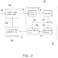
- FIG. 3 is a block diagram illustrating the clock recovery apparatus 10 according to an embodiment of the invention.
- the clock recovery circuit 130 shown in FIG. 3 further includes a phase detector 131, a loop filter 132, a phase-offset estimator 133, and a phase adjusting circuit 134.
- the phase detector 131 is coupled to the analog-to-digital converter 110, and receives the digital input signal A1 and performs phase detection on the digital input signal A1 to generate a phase indication signal P_h to indicate the phase shift of the digital input signal A1.
- the phase detector 131 may detect the phase shift of the digital input signal A1 by various algorithms to generate the phase indication signal P_h, so as to indicate the phase difference between the sampling clock CLK and the working clock of the transmitting end of the analog input signal R1.
- the phase detector 131 may estimate the phase shift of the digital input signal A1 by using a maximum likelihood algorithm or a minimum mean square error (MMSE) algorithm. Nevertheless, the invention is not limited thereto.
- the loop filter 132 is coupled to the phase detector 131 and filters the phase indication signal P_h to generate a phase control signal P_c.
- the loop filter 132 may be implemented by a proportional integral filter, for example. Nevertheless, the invention is not limited thereto.
- the phase-offset estimator 133 is coupled to the loop filter 132 and estimates the phase-offset parameter and a phase adjustment direction in the first period by counting the number of pulses of the phase control signal P_c in an estimation window.
- the phase adjusting circuit 134 is coupled to the loop filter 132 and the phase-offset estimator 133, and generates the phase selection signal P1 according to the phase control signal P_c in the first period. That is, during the first period, the phase adjusting circuit 134 may control the phase selection signal P1 to form a pulse according to the output of the loop filter 132, and the multi-phase clock generating circuit 120 may advance or retard the sampling clock CLK by one phase in response to the pulse.
- the phase-offset estimator 133 During the second period, the phase-offset estimator 133 generates an automatic adjustment signal C1 according to the phase-offset parameter and the phase adjustment direction, and the phase adjusting circuit 134 generates the phase selection signal according to the automatic adjustment signal C1 and the phase control signal P_c in the second period.
- the phase adjusting circuit 134 may control the phase selection signal P1 according to the output signals (i.e. the phase control signal P_c and the automatic adjustment signal C1) of the loop filter 132 and the phase-offset estimator 133 to form the pulse, and the multi-phase clock generating circuit 120 may advance or retard the sampling clock CLK by one phase in response to the pulse.
- the phase-offset estimator 133 may continue counting the number of pulses of the phase control signal P_c in the estimation window, so as to correct the phase-offset parameter estimated in the first period.
- the window length of the estimation window used by the loop filter 132 in the first period is different from the window length of the estimation window used in the second period, and the window length of the estimation window used by the loop filter 132 in the second period is longer.
- the loop filter 132 in the second period may be implemented by an infinite impulse response filter (IIR), for example. Nevertheless, the invention is not limited thereto.
- the phase-offset estimator 133 may include a numerically controlled oscillator (NCO) established based on the phase-offset parameter, so as to timely control the automatic adjustment signal C1 to form the pulse according to the phase-offset parameter.
- NCO numerically controlled oscillator
- FIG. 4 is a block diagram illustrating the clock recovery circuit 130 according to an embodiment of the invention.
- the phase control signal P_c includes a phase advanced control signal ted_adv and a phase retarded control signal ted_ret
- the phase selection signal P1 includes an advanced control signal PLL_ADV and a retarded control signal PLL_RET
- the automatic control signal C1 includes an estimation advanced control signal fw_adv and an estimation retarded control signal fw_ret.
- the multi-phase clock generating circuit 120 advances the sampling clock CLK by one phase in response to the pulse of the advanced control signal PLL_ADV or retards the sampling clock CLK by one phase in response to the pulse of the retarded control signal PLL_RET.
- the phase adjusting circuit 134 generates the advanced control signal PLL_ADV according to the phase advanced control signal ted_adv and the estimation advanced control signal fw_adv, and the phase adjusting circuit 134 generates the retarded control signal PLL_RET according to the phase retarded control signal ted_ret and the estimation retarded control signal fw_ret.
- the phase-offset estimator 133 includes an estimating circuit 133_1 and a numerically controlled oscillator 133_2.
- the estimating circuit 133_1 receives the phase advanced control signal ted_adv and the phase retarded control signal ted_ret and estimates a phase-offset parameter offset_s according to the phase advanced control signal ted_adv and the phase retarded control signal ted_ret.
- the numerically controlled oscillator 133_2 obtains the phase-offset parameter offset_s from the estimating circuit 133_1 and accumulates the phase-offset parameter offset_s to obtain an accumulated result.
- the numerically controlled oscillator 133_2 controls the estimation advanced control signal fw_adv and the estimation retarded control signal fw_ret to form a pulse according to the phase adjustment direction.
- the estimating circuit 133_1 counts a pulse number adv_cnt of the phase advanced control signal ted_adv and a pulse number ret_cnt of the phase retarded control signal ted_ret in the estimation window (assumed to be N clocks). Then, the estimating circuit 133_1 compares the pulse numbers of the two signals to determine the phase adjustment direction. Specifically, the estimating circuit 133_1 may subtract the pulse number ret_cnt from the pulse number adv_cnt to obtain a pulse number difference M and determine the phase adjustment direction based on whether the pulse number difference M is positive or negative. Moreover, assuming that the multi-phase clock generating circuit 120 may provide 128 phase options, the phase-offset parameter offset_s may be obtained by the following Equation (1).
- offset_s M 128 N
- the pulse number difference M is greater than 0, and accordingly the estimating circuit 133_1 determines that the phase adjustment direction is to advance.
- the phase-offset parameter offset_s at the moment is equal to 83.45ppm.
- the decimal place accuracy may be designed according to the actual requirements.
- the numerically controlled oscillator 133_2 may control the estimation advanced control signal fw_adv or the estimation retarded control signal fw_ret to form the pulse according to the phase-offset parameter offset_s and the phase adjustment direction.
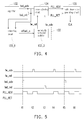
- FIG. 5 is a signal timing diagram of the clock recovery circuit according to an embodiment of the invention.
- the loop filter 132 detects that the phase of the sampling clock CLK requires adjustment according to the phase indication signal P_h, in which the phase indication signal P_h is for indicating the phase shift of the digital input signal A1. Therefore, the loop filter 132 controls the phase advanced control signal ted_adv to form a pulse, and at the same time, the phase adjusting circuit 134 controls the advanced control signal PLL_ADV to form a pulse at the time point t1 in response to the pulse of the phase advanced control signal ted_adv. Therefore, the multi-phase clock generating circuit 120 advances the sampling clock CLK by one phase in response to the pulse of the advanced control signal PLL ADV at the time point t1.
- the numerically controlled oscillator 133_2 controls the estimation advanced control signal fw_adv according to the phase-offset parameter offset_s to form a pulse
- the phase adjusting circuit 134 controls the advanced control signal PLL_ADV to form a pulse at the time point t2 in response to the pulse of the estimation advanced control signal fw_adv. Therefore, the multi-phase clock generating circuit 120 advances the sampling clock CLK by one phase in response to the pulse of the advanced control signal PLL_ADV at the time point t2.
- the loop filter 132 detects that the phase of the sampling clock CLK requires adjustment according to the phase indication signal P_h. Therefore, the loop filter 132 controls the phase retarded control signal ted_ret to form a pulse, and at the same time, the phase adjusting circuit 134 controls the retarded control signal PLL_RET to form a pulse at the time point t3 in response to the pulse of the phase retarded control signal ted_ret.
- the multi-phase clock generating circuit 120 retards the sampling clock CLK by one phase in response to the pulse of the retarded control signal PLL_RET at the time point t3.
- the numerically controlled oscillator 133_2 controls the estimation advanced control signal fw_adv to form a pulse according to the phase-offset parameter offset_s
- the phase adjusting circuit 134 controls the advanced control signal PLL_ADV to form pulses at the time points t4 and t6 in response to the pulse of the estimation advanced control signal fw_adv.
- the multi-phase clock generating circuit 120 advances the sampling clock CLK by one phase in response to the pulses of the advanced control signal PLL_ADV at the time points t4 and t6.
- the loop filter 132 detects that the phase of the sampling clock CLK requires adjustment according to the phase indication signal P_h. Therefore, the loop filter 132 controls the phase advanced control signal ted_adv to form a pulse, and at the same time, the phase adjusting circuit 134 controls the advanced control signal PLL_ADV to form a pulse at the time point t5 in response to the pulse of the phase advanced control signal ted_adv.
- the multi-phase clock generating circuit 120 advances the sampling clock CLK by one phase in response to the pulse of the advanced control signal PLL_ADV at the time point t5.
- the pulses on the estimation advanced control signal fw_adv and the estimation retarded control signal fw_ret are formed automatically according to the phase-offset parameter while the phase advanced control signal ted_adv and the phase retarded control signal ted_ret are generated by instant detection of the phase detector 131 and the loop filter 132.
- all the estimation advanced control signal fw_adv, estimation retarded control signal fw_ret, phase advanced control signal ted_adv, and phase retarded control signal ted_ret may control the advanced control signal PLL_ADV and the retarded control signal PLL_RET to form pulses, so as to change the phase of the sampling clock CLK.
- FIG. 6 is a flowchart illustrating the numerically controlled oscillator generating the automatic adjustment signal according to an embodiment of the invention.
- Step S601 the numerically controlled oscillator 133_2 initializes the accumulated result. In other words, the numerically controlled oscillator 133_2 resets the accumulated result to 0.
- Step S602 the numerically controlled oscillator 133_2 periodically accumulates the phase-offset parameter offset_s to the accumulated result. Specifically, the numerically controlled oscillator 133_2 accumulates one phase-offset parameter offset_s to the accumulated result in each clock cycle in response to the clock signal (i.e. the sampling clock CLK in this embodiment).
- Step S603 the numerically controlled oscillator 133_2 determines whether the accumulated result is greater than the predetermined phase difference. If the result of Step S603 is No, the numerically controlled oscillator 133_2 continues accumulating the phase-offset parameter offset_s.
- Step S604 the numerically controlled oscillator 133_2 determines whether the phase adjustment direction is to advance. If the result of Step S604 is Yes, in Step S605, the numerically controlled oscillator 133_2 controls the estimation advanced control signal fw_adv to generate a pulse. If the result of Step S604 is No, in Step S606, the numerically controlled oscillator 133_2 controls the estimation retarded control signal fw_ret to generate a pulse. In Step S607, the numerically controlled oscillator 133_2 subtracts a unit-adjustable phase from the accumulated result and returns to Step S602. The unit-adjustable phase is determined by the number of phases that the multi-phase clock generating circuit 120 can provide. Take the multi-phase clock generating circuit 120 that has 128 phases for example, the unit-adjustable phase is 1/128(Ts).
- the clock recovery circuit of the invention is able to count the number of times that the output phase of the sampling clock is adjusted based on the phase difference detection result in the first period, so as to estimate the phase-offset parameter.
- the phase-offset estimator may establish the numerically controlled oscillator by using the phase-offset parameter, so as to control the multi-phase clock generating circuit to automatically adjust the phase of the sampling clock.
- the clock recovery apparatus of the invention coordinates the phase-offset estimator and the existing phase difference detecting circuit to accurately lock the oscillating clocks of the receiving end and further improve the performance of the Ethernet physical layer in long-term transmission or the operating environment of greater phase offset.
Landscapes
- Engineering & Computer Science (AREA)
- Computer Networks & Wireless Communication (AREA)
- Signal Processing (AREA)
- Synchronisation In Digital Transmission Systems (AREA)
- Stabilization Of Oscillater, Synchronisation, Frequency Synthesizers (AREA)
Abstract
Description
- The invention relates to a clock synchronization circuit and more particularly relates to a clock recovery apparatus and a clock recovery method.
- With the development of technology, the Internet has become a necessary configuration for exchanging information. Among various network configurations, Ethernet has characteristics such as easily accessible, easy to build, fast transmission, and so on, which contribute to the thriving development of Ethernet-related equipment, and the transmission rate thereof also increases from 10Mbps to 100Mbps or even 1 Gbps. In order to satisfy the growing demand for packet switching network, Ethernet is constantly evolving. For example, Gigabit Ethernet is defined in the IEEE 802.3 standard. The 1000Base-T standard is one standard protocol that is applied to a coaxial cable and defined in IEEE 802.3ab. It can be foreseen that as the data transmission speed increases, the requirement for clock synchronization and clock accuracy at the receiving end and the transmitting end will get stricter as well.
- Furthermore, in the network physical layer (PHY) of Ethernet equipment, in order to ensure the accuracy of the data recovered by the receiving end circuit, ideally the sampling clock generated by the phase locked loop (PLL) of the transmitting end and the sampling clock generated by the phase locked loop (PLL) of the receiving end should have the same frequency, so that the receiving end can correctly recover the data transmitted by the transmitting end. However, frequency offset may exist in the local oscillation by which the receiving end or the transmitting end generates the sampling clock. Consequently, the sampling clocks of the receiving end and the transmitting end may not be synchronized. Thus, a clock recovery apparatus is provided in the network physical layer (PHY) for correcting the non-synchronization caused by the phase offset, so that the sampling clocks of the receiving end and the transmitting end can be synchronized. The conventional clock recovery apparatus locks the output phase of PLL by collecting statistics regarding variation of phase difference in the statistical window with a fixed length. In long-term transmission or an operating environment with greater phase offset, however, the statistical properties generated by the loop filter of the conventional clock recovery apparatus may not be obvious enough to serve as the reference for locking the output phase of PLL. In particular, it is very inflexible to use the statistical window with a fixed length to estimate the unpredictable phase offset. It is possible that the output phase of PLL may not be adjusted in time if the phase offset is excessively large and the statistical window is excessively long.
- The invention provides a clock recovery apparatus and a clock recovery method, which more accurately synchronize the sampling clocks of the receiving and transmitting ends to reduce the packet error rate and improve performance of the Ethernet physical layer.
- The invention provides a clock recovery apparatus, which includes an analog-to-digital converter, a multi-phase clock generating circuit, and a clock recovery circuit. The analog-to-digital converter samples an analog input signal by a sampling clock to output a digital input signal. The multi-phase clock generating circuit is coupled to the analog-to-digital converter, and outputs the sampling clock to the analog-to-digital converter and controls a phase of the sampling clock according to a phase selection signal. The clock recovery circuit is coupled to the analog-to-digital converter and the multi-phase clock generating circuit and receives the digital input signal. During a first period, the clock recovery circuit detects a phase shift of the digital input signal to generate the phase selection signal and estimates a phase-offset parameter according to the digital input signal. During a second period, the clock recovery circuit generates the phase selection signal according to the phase-offset parameter generated in the first period and the phase shift of the digital input signal.
- In an embodiment of the invention, the clock recovery circuit includes a phase detector, a loop filter, a phase-offset estimator, and a phase adjusting circuit. The phase detector is coupled to the analog-to-digital converter and the multi-phase clock generating circuit and performs phase detection on the digital input signal to generate a phase indication signal indicating the phase shift of the digital input signal. The loop filter is coupled to the phase detector and filters the phase indication signal to generate a phase control signal. The phase-offset estimator is coupled to the loop filter and estimates the phase-offset parameter and a phase adjustment direction in the first period by counting a pulse number of the phase control signal in an estimation window. The phase adjusting circuit is coupled to the loop filter and the phase-offset estimator and outputs the phase selection signal.
- In an embodiment of the invention, the phase-offset estimator generates an automatic adjustment signal according to the phase-offset parameter and the phase adjustment direction in the second period, and the phase adjusting circuit generates the phase selection signal according to the automatic adjustment signal and the phase control signal in the second period.
- In an embodiment of the invention, the phase adjusting circuit generates the phase selection signal according to the phase control signal in the first period.
- In an embodiment of the invention, the phase-offset estimator includes a numerically controlled oscillator established based on the phase-offset parameter, and the numerically controlled oscillator initializes an accumulated result. The numerically controlled oscillator periodically accumulates the phase-offset parameter to the accumulated result. When the accumulated result is greater than a predetermined phase difference, the numerically controlled oscillator controls the automatic adjustment signal to provide a pulse according to the phase adjustment direction.
- In an embodiment of the invention, the multi-phase clock generating circuit generates a plurality of clock signals and selects one of the clock signals to serve as the sampling clock according to the phase selection signal. The clock signals have the same frequency and different phases.
- From another aspect, the invention provides a clock recovery method, which includes the following. An analog input signal is received and the analog input signal is sampled according to a sampling clock to generate a digital input signal. In a first period, a phase shift of the digital input signal is detected to generate a phase selection signal so as to determine a phase of the sampling clock according to the phase selection signal. In the first period, a phase-offset parameter is estimated according to the digital input signal. In a second period, the phase selection signal is generated according to the phase-offset parameter generated in the first period and the phase shift of the digital input signal, so as to determine the phase of the sampling clock according to the phase selection signal.
- Based on the above, the clock recovery apparatus of the invention is further provided with the phase-offset estimator, which counts the number of times of phase adjustments in the first period, so as to estimate the phase-offset parameter. In the second period, the phase-offset estimator may establish the numerically controlled oscillator by using the phase-offset parameter, so as to predict whether the current phase shift exceeds the predetermined phase difference according to the phase-offset parameter. If the phase-offset estimator predicts that the current phase shift has exceeded the predetermined phase difference, the phase-offset estimator may control the multi-phase clock generating circuit to automatically adjust the phase of the sampling clock accordingly, so as to synchronize the sampling clocks of the receiving and transmitting ends in the Ethernet network.
- To make the aforementioned and other features and advantages of the invention more comprehensible, several embodiments accompanied with drawings are described in detail as follows.
-
-
FIG. 1 is a block diagram illustrating the clock recovery apparatus according to an embodiment of the invention. -
FIG. 2 is a flowchart illustrating the clock recovery method according to an embodiment of the invention. -
FIG. 3 is a block diagram illustrating the clock recovery apparatus according to an embodiment of the invention. -
FIG. 4 is a block diagram illustrating the clock recovery circuit according to an embodiment of the invention. -
FIG. 5 is a flowchart of the numerically controlled oscillator generating the automatic adjustment signal according to an embodiment of the invention. -
FIG. 6 is a signal timing diagram of the clock recovery circuit according to an embodiment of the invention. -
FIG. 1 is a block diagram illustrating aclock recovery apparatus 10 according to an embodiment of the invention. Theclock recovery apparatus 10 is configured for generating a clock required by an Ethernet physical layer and for synchronizing clocks of receiving and transmitting ends, and may be disposed in an Ethernet transceiver of 1000Base-T, for example. Nevertheless, the invention is not limited thereto. Theclock recovery apparatus 10 includes an analog-to-digital converter (ADC) 110, a multi-phaseclock generating circuit 120, and aclock recovery circuit 130. The analog-to-digital converter 110 samples an analog input signal R1 according to a sampling clock CLK and outputs a digital input signal A1. Specifically, the analog-to-digital converter 110 of theclock recovery apparatus 10 may receive the analog input signal R1 transmitted by a coaxial cable or twisted pair via an Ethernet interface, and perform digital-analog conversion on the analog input signal R1 to output the digital input signal A1. - The multi-phase
clock generating circuit 120 is coupled to the analog-to-digital converter 110, and outputs the sampling clock CLK to the analog-to-digital converter 110 and controls a phase of the sampling clock CLK according to a phase selection signal P1. In an embodiment, the multi-phaseclock generating circuit 120 may generate a plurality of clock signals and output one of the clock signals as the sampling clock CLK according to the phase selection signal P1. The clock signals are provided with the same frequency but different phases. For example, the multi-phaseclock generating circuit 120 may be a 128-phase clock generator, which may generate a plurality of clock signals corresponding to 128 phases and output one of the 128 clock signals as the sampling clock CLK according to the phase selection signal P1. To be more specific, the multi-phaseclock generating circuit 120 may advance or retard the outputted sampling clock CLK by one phase in response to a pulse of the phase selection signal P1. - The
clock recovery circuit 130 is coupled to the analog-to-digital converter 110 and the multi-phaseclock generating circuit 120 and receives the digital input signal A1. During a first period, in an embodiment, theclock recovery circuit 130 detects a phase shift of the digital input signal A1 to generate the phase selection signal P1, and estimates a phase-offset parameter according to a statistical result of the phase shift of the digital input signal A1. Specifically, the phase shift of the digital input signal A1 results from a frequency difference between the sampling clock CLK and a working clock of the transmitting end that outputs the analog input signal R1. Then, during a second period, theclock recovery circuit 130 generates the phase selection signal P1 according to the phase-offset parameter generated in the first period and the phase shift of the digital input signal A1. That is, theclock recovery apparatus 10 may estimate a phase-offset state between the working clock of the transmitting end that outputs the analog input signal R1 and the sampling clock CLK in advance in the first period. Accordingly, theclock recovery apparatus 10 may automatically adjust the output phase of the multi-phaseclock generating circuit 120 according to the estimated phase-offset parameter in the second period and simultaneously correct the residual phase-offset according to the phase shift state of the digital input signal A1. -
FIG. 2 is a flowchart illustrating a clock recovery method according to an embodiment of the invention. In this embodiment, the clock recovery method may be applied to theclock recovery apparatus 10 ofFIG. 1 , but the invention is not limited thereto. - Referring to
FIG. 2 , in Step S201, the analog-to-digital converter 110 receives the analog input signal R1 and samples the analog input signal R1 according to the sampling clock CLK to generate the digital input signal A1. In Step S202, during the first period, theclock recovery circuit 130 detects the phase shift of the digital input signal A1 to generate the phase selection signal P1, and the multi-phaseclock generating circuit 120 determines the phase of the sampling clock CLK according to the phase selection signal P1. In Step S203, during the first period, theclock recovery circuit 130 estimates the phase-offset parameter according to the digital input signal A1. In Step S204, during the second period, theclock recovery circuit 130 generates the phase selection signal P1 according to the phase-offset parameter generated in the first period and the phase shift of the digital input signal A1, such that the multi-phaseclock generating circuit 120 determines the phase of the sampling clock CLK according to the phase selection signal P1. Accordingly, by estimating the phase-offset parameter in the first period, theclock recovery apparatus 10 may automatically adjust the phase of the sampling clock CLK by using the phase-offset parameter in the second period. Thus, even in an operating environment where the phase-offset between the receiving and transmitting ends is large, theclock recovery apparatus 10 is still able to recover the phase of the sampling clock CLK to a state close to the phase of the clock signal of the transmitting end. -
FIG. 3 is a block diagram illustrating theclock recovery apparatus 10 according to an embodiment of the invention. Referring toFIG. 3 , theclock recovery circuit 130 shown inFIG. 3 further includes aphase detector 131, aloop filter 132, a phase-offsetestimator 133, and aphase adjusting circuit 134. Thephase detector 131 is coupled to the analog-to-digital converter 110, and receives the digital input signal A1 and performs phase detection on the digital input signal A1 to generate a phase indication signal P_h to indicate the phase shift of the digital input signal A1. Simply put, when thephase detector 131 receives the digital input signal A1, thephase detector 131 may detect the phase shift of the digital input signal A1 by various algorithms to generate the phase indication signal P_h, so as to indicate the phase difference between the sampling clock CLK and the working clock of the transmitting end of the analog input signal R1. For example, thephase detector 131 may estimate the phase shift of the digital input signal A1 by using a maximum likelihood algorithm or a minimum mean square error (MMSE) algorithm. Nevertheless, the invention is not limited thereto. - The
loop filter 132 is coupled to thephase detector 131 and filters the phase indication signal P_h to generate a phase control signal P_c. Theloop filter 132 may be implemented by a proportional integral filter, for example. Nevertheless, the invention is not limited thereto. - The phase-offset
estimator 133 is coupled to theloop filter 132 and estimates the phase-offset parameter and a phase adjustment direction in the first period by counting the number of pulses of the phase control signal P_c in an estimation window. Thephase adjusting circuit 134 is coupled to theloop filter 132 and the phase-offsetestimator 133, and generates the phase selection signal P1 according to the phase control signal P_c in the first period. That is, during the first period, thephase adjusting circuit 134 may control the phase selection signal P1 to form a pulse according to the output of theloop filter 132, and the multi-phaseclock generating circuit 120 may advance or retard the sampling clock CLK by one phase in response to the pulse. - During the second period, the phase-offset
estimator 133 generates an automatic adjustment signal C1 according to the phase-offset parameter and the phase adjustment direction, and thephase adjusting circuit 134 generates the phase selection signal according to the automatic adjustment signal C1 and the phase control signal P_c in the second period. Specifically, thephase adjusting circuit 134 may control the phase selection signal P1 according to the output signals (i.e. the phase control signal P_c and the automatic adjustment signal C1) of theloop filter 132 and the phase-offsetestimator 133 to form the pulse, and the multi-phaseclock generating circuit 120 may advance or retard the sampling clock CLK by one phase in response to the pulse. - It should be noted that, during the second period, the phase-offset
estimator 133 may continue counting the number of pulses of the phase control signal P_c in the estimation window, so as to correct the phase-offset parameter estimated in the first period. In addition, the window length of the estimation window used by theloop filter 132 in the first period is different from the window length of the estimation window used in the second period, and the window length of the estimation window used by theloop filter 132 in the second period is longer. In an embodiment, theloop filter 132 in the second period may be implemented by an infinite impulse response filter (IIR), for example. Nevertheless, the invention is not limited thereto. - In an embodiment of the invention, the phase-offset
estimator 133 may include a numerically controlled oscillator (NCO) established based on the phase-offset parameter, so as to timely control the automatic adjustment signal C1 to form the pulse according to the phase-offset parameter. An embodiment is described in detail below as an example. -
FIG. 4 is a block diagram illustrating theclock recovery circuit 130 according to an embodiment of the invention. It should be noted that, in this embodiment, the phase control signal P_c includes a phase advanced control signal ted_adv and a phase retarded control signal ted_ret; the phase selection signal P1 includes an advanced control signal PLL_ADV and a retarded control signal PLL_RET; and the automatic control signal C1 includes an estimation advanced control signal fw_adv and an estimation retarded control signal fw_ret. In an embodiment, the multi-phaseclock generating circuit 120 advances the sampling clock CLK by one phase in response to the pulse of the advanced control signal PLL_ADV or retards the sampling clock CLK by one phase in response to the pulse of the retarded control signal PLL_RET. - In this embodiment, the
phase adjusting circuit 134 generates the advanced control signal PLL_ADV according to the phase advanced control signal ted_adv and the estimation advanced control signal fw_adv, and thephase adjusting circuit 134 generates the retarded control signal PLL_RET according to the phase retarded control signal ted_ret and the estimation retarded control signal fw_ret. - The phase-offset
estimator 133 includes an estimating circuit 133_1 and a numerically controlled oscillator 133_2. The estimating circuit 133_1 receives the phase advanced control signal ted_adv and the phase retarded control signal ted_ret and estimates a phase-offset parameter offset_s according to the phase advanced control signal ted_adv and the phase retarded control signal ted_ret. The numerically controlled oscillator 133_2 obtains the phase-offset parameter offset_s from the estimating circuit 133_1 and accumulates the phase-offset parameter offset_s to obtain an accumulated result. When the accumulated result is greater than a predetermined phase difference, the numerically controlled oscillator 133_2 controls the estimation advanced control signal fw_adv and the estimation retarded control signal fw_ret to form a pulse according to the phase adjustment direction. - In this embodiment, the estimating circuit 133_1 counts a pulse number adv_cnt of the phase advanced control signal ted_adv and a pulse number ret_cnt of the phase retarded control signal ted_ret in the estimation window (assumed to be N clocks). Then, the estimating circuit 133_1 compares the pulse numbers of the two signals to determine the phase adjustment direction. Specifically, the estimating circuit 133_1 may subtract the pulse number ret_cnt from the pulse number adv_cnt to obtain a pulse number difference M and determine the phase adjustment direction based on whether the pulse number difference M is positive or negative. Moreover, assuming that the multi-phase
clock generating circuit 120 may provide 128 phase options, the phase-offset parameter offset_s may be obtained by the following Equation (1).
- For example, assuming that a length N of the estimation window is 216 clock cycles (N=216) and the pulse number adv_cnt counted by the estimating circuit 133_1 in the estimation window is equal to 1000 and the pulse number ret_cnt is equal to 300, the pulse number difference M is equal to 700 (M=1000-300=700). The pulse number difference M is greater than 0, and accordingly the estimating circuit 133_1 determines that the phase adjustment direction is to advance. According to the Equation (1), the phase-offset parameter offset_s at the moment is equal to 83.45ppm. The decimal place accuracy may be designed according to the actual requirements. Thus, the numerically controlled oscillator 133_2 may control the estimation advanced control signal fw_adv or the estimation retarded control signal fw_ret to form the pulse according to the phase-offset parameter offset_s and the phase adjustment direction.
-
FIG. 5 is a signal timing diagram of the clock recovery circuit according to an embodiment of the invention. Referring toFIG. 4 and FIG. 5 , at a time point t1, theloop filter 132 detects that the phase of the sampling clock CLK requires adjustment according to the phase indication signal P_h, in which the phase indication signal P_h is for indicating the phase shift of the digital input signal A1. Therefore, theloop filter 132 controls the phase advanced control signal ted_adv to form a pulse, and at the same time, thephase adjusting circuit 134 controls the advanced control signal PLL_ADV to form a pulse at the time point t1 in response to the pulse of the phase advanced control signal ted_adv. Therefore, the multi-phaseclock generating circuit 120 advances the sampling clock CLK by one phase in response to the pulse of the advanced control signal PLL ADV at the time point t1. - At a time point t2, the numerically controlled oscillator 133_2 controls the estimation advanced control signal fw_adv according to the phase-offset parameter offset_s to form a pulse, and at the same time, the
phase adjusting circuit 134 controls the advanced control signal PLL_ADV to form a pulse at the time point t2 in response to the pulse of the estimation advanced control signal fw_adv. Therefore, the multi-phaseclock generating circuit 120 advances the sampling clock CLK by one phase in response to the pulse of the advanced control signal PLL_ADV at the time point t2. - At a time point t3, the
loop filter 132 detects that the phase of the sampling clock CLK requires adjustment according to the phase indication signal P_h. Therefore, theloop filter 132 controls the phase retarded control signal ted_ret to form a pulse, and at the same time, thephase adjusting circuit 134 controls the retarded control signal PLL_RET to form a pulse at the time point t3 in response to the pulse of the phase retarded control signal ted_ret. Thus, the multi-phaseclock generating circuit 120 retards the sampling clock CLK by one phase in response to the pulse of the retarded control signal PLL_RET at the time point t3. - Similarly, at time points t4 and t6, the numerically controlled oscillator 133_2 controls the estimation advanced control signal fw_adv to form a pulse according to the phase-offset parameter offset_s, and at the same time, the
phase adjusting circuit 134 controls the advanced control signal PLL_ADV to form pulses at the time points t4 and t6 in response to the pulse of the estimation advanced control signal fw_adv. Thus, the multi-phaseclock generating circuit 120 advances the sampling clock CLK by one phase in response to the pulses of the advanced control signal PLL_ADV at the time points t4 and t6. At a time point t5, theloop filter 132 detects that the phase of the sampling clock CLK requires adjustment according to the phase indication signal P_h. Therefore, theloop filter 132 controls the phase advanced control signal ted_adv to form a pulse, and at the same time, thephase adjusting circuit 134 controls the advanced control signal PLL_ADV to form a pulse at the time point t5 in response to the pulse of the phase advanced control signal ted_adv. Thus, the multi-phaseclock generating circuit 120 advances the sampling clock CLK by one phase in response to the pulse of the advanced control signal PLL_ADV at the time point t5. - Based on the above, it is known that the pulses on the estimation advanced control signal fw_adv and the estimation retarded control signal fw_ret are formed automatically according to the phase-offset parameter while the phase advanced control signal ted_adv and the phase retarded control signal ted_ret are generated by instant detection of the
phase detector 131 and theloop filter 132. However, all the estimation advanced control signal fw_adv, estimation retarded control signal fw_ret, phase advanced control signal ted_adv, and phase retarded control signal ted_ret may control the advanced control signal PLL_ADV and the retarded control signal PLL_RET to form pulses, so as to change the phase of the sampling clock CLK. - An embodiment is provided below to describe in detail how the numerically controlled oscillator 133_2 generates the estimation advanced control signal fw_adv and the estimation retarded control signal fw_ret of the automatic adjustment signal C1 according to the phase-offset parameter offset_s.
FIG. 6 is a flowchart illustrating the numerically controlled oscillator generating the automatic adjustment signal according to an embodiment of the invention. - Referring to
FIG. 6 , in Step S601, the numerically controlled oscillator 133_2 initializes the accumulated result. In other words, the numerically controlled oscillator 133_2 resets the accumulated result to 0. In Step S602, the numerically controlled oscillator 133_2 periodically accumulates the phase-offset parameter offset_s to the accumulated result. Specifically, the numerically controlled oscillator 133_2 accumulates one phase-offset parameter offset_s to the accumulated result in each clock cycle in response to the clock signal (i.e. the sampling clock CLK in this embodiment). In Step S603, the numerically controlled oscillator 133_2 determines whether the accumulated result is greater than the predetermined phase difference. If the result of Step S603 is No, the numerically controlled oscillator 133_2 continues accumulating the phase-offset parameter offset_s. - If the result of Step S603 is Yes, in Step S604, the numerically controlled oscillator 133_2 determines whether the phase adjustment direction is to advance. If the result of Step S604 is Yes, in Step S605, the numerically controlled oscillator 133_2 controls the estimation advanced control signal fw_adv to generate a pulse. If the result of Step S604 is No, in Step S606, the numerically controlled oscillator 133_2 controls the estimation retarded control signal fw_ret to generate a pulse. In Step S607, the numerically controlled oscillator 133_2 subtracts a unit-adjustable phase from the accumulated result and returns to Step S602. The unit-adjustable phase is determined by the number of phases that the multi-phase
clock generating circuit 120 can provide. Take the multi-phaseclock generating circuit 120 that has 128 phases for example, the unit-adjustable phase is 1/128(Ts). - In conclusion, by additionally disposing the phase-offset estimator, the clock recovery circuit of the invention is able to count the number of times that the output phase of the sampling clock is adjusted based on the phase difference detection result in the first period, so as to estimate the phase-offset parameter. In the second period, the phase-offset estimator may establish the numerically controlled oscillator by using the phase-offset parameter, so as to control the multi-phase clock generating circuit to automatically adjust the phase of the sampling clock. Overall, the clock recovery apparatus of the invention coordinates the phase-offset estimator and the existing phase difference detecting circuit to accurately lock the oscillating clocks of the receiving end and further improve the performance of the Ethernet physical layer in long-term transmission or the operating environment of greater phase offset.
Claims (13)
- A clock recovery apparatus (10), comprising:an analog-to-digital converter (110) sampling an analog input signal (R1) by using a sampling clock (CLK) to output a digital input signal (A1);a multi-phase clock generating circuit (120) coupled to the analog-to-digital converter (110) and outputting the sampling clock (CLK) to the analog-to-digital converter (110) and controlling a phase of the sampling clock (CLK) according to a phase selection signal (P1); anda clock recovery circuit (130) coupled to the analog-to-digital converter (110) and the multi-phase clock generating circuit (120) and receiving the digital input signal (A1),wherein in a first period, the clock recovery circuit (130) detects a phase shift of the digital input signal (A1) to generate the phase selection signal (P1) and estimates a phase-offset parameter according to the digital input signal (A1), and
in a second period, the clock recovery circuit (130) generates the phase selection signal (P1) according to the phase-offset parameter generated in the first period and the phase shift of the digital input signal (A1). - The clock recovery apparatus according to claim 1, wherein the clock recovery circuit (130) comprises:a phase detector (131) coupled to the analog-to-digital converter (110) and performing phase detection on the digital input signal (A1) to generate a phase indication signal (P_h) indicating the phase shift of the digital input signal (A1);a loop filter (132) coupled to the phase detector (131) and filtering the phase indication signal (P_h) to generate a phase control signal (P_c);a phase-offset estimator (133) coupled to the loop filter (132) and estimating the phase-offset parameter and a phase adjustment direction in the first period by counting a pulse number of the phase control signal in an estimation window; anda phase adjusting circuit (134) coupled to the loop filter (132) and the phase-offset estimator (133) and outputting the phase selection signal (P1).
- The clock recovery apparatus according to claim 1 or 2, wherein the phase-offset estimator (134) generates an automatic adjustment signal (C1) in the second period according to the phase-offset parameter and the phase adjustment direction, and the phase adjusting circuit (134) generates the phase selection signal (P1) in the second period according to the automatic adjustment signal (C1) and the phase control signal (P_c).
- The clock recovery apparatus according to claim 2 or 3, wherein the phase-offset estimator (133) comprises a numerically controlled oscillator (133_2) established based on the phase-offset parameter, and the numerically controlled oscillator (133_2) initializes an accumulated result and periodically accumulates the phase-offset parameter to the accumulated result, and when the accumulated result is greater than a predetermined phase difference, the numerically controlled oscillator (133_2) controls the automatic adjustment signal (C1) to provide a pulse according to the phase adjustment direction.
- The clock recovery apparatus according to any of the claims 2 to 4, wherein the phase adjusting circuit (134) generates the phase selection signal (P1) according to the phase control signal (P_c) in the first period.
- The clock recovery apparatus according to any of the claims 2 to 5, wherein the multi-phase clock generating circuit (120) generates a plurality of clock signals and selects one of the clock signals as the sampling clock (CLK) according to the phase selection signal (P1), wherein the clock signals are provided with the same frequency and different phases.
- A clock recovery method, comprising:receiving (S201) an analog input signal (R1) and sampling the analog input signal (R1) according to a sampling clock (CLK) to generate a digital input signal (A1);in a first period, detecting (S202) a phase shift of the digital input signal (A1) to generate a phase selection signal (P1) and determining a phase of the sampling clock (CLK) according to the phase selection signal (P1);in the first period, estimating (S203) a phase-offset parameter according to the digital input signal (A1); andin a second period, generating (S204) the phase selection signal (P1) according to the phase-offset parameter generated in the first period and the phase shift of the digital input signal (A1).
- The clock recovery method according to claim 7, further comprising:in the second period, correcting the phase-offset parameter according to the digital input signal (A1), and generating the phase selection signal (P1) according to the corrected phase-offset parameter and the phase shift of the digital input signal (A1).
- The clock recovery method according to claim 7 or 8, wherein the step of generating the phase selection signal (P1) according to the phase shift of the digital input signal (A1) in the first period comprises:performing phase detection on the digital input signal (A1) to generate a phase indication signal (P_h) indicating the phase shift of the digital input signal;filtering the phase indication signal (P_h) to generate a phase control signal (P_c); andoutputting the phase selection signal (P1) according to the phase control signal (P_c) to determine the phase of the sampling clock (CLK).
- The clock recovery method according to claim 9, wherein the step of estimating the phase-offset parameter according to the digital input signal (A1) and the sampling clock (CLK) in the first period comprises:estimating the phase-offset parameter and a phase adjustment direction in the first period by counting a pulse number of the phase control signal (P_c) in an estimation window.
- The clock recovery method according to claim 9 or 10, wherein the step of generating the phase selection signal (P1) according to the phase-offset parameter and the phase shift of the digital input signal (A1) in the second period comprises:generating an automatic adjustment signal (C1) in the second period according to the phase-offset parameter and the phase adjustment direction and generating the phase selection signal (P1) according to the automatic adjustment signal (C1) and the phase control signal (P_c).
- The clock recovery method according to claim 11, wherein the step of generating the automatic adjustment signal (C1) in the second period according to the phase-offset parameter and the phase adjustment direction, and generating the phase selection signal (P1) according to the automatic adjustment signal (C1) and the phase control signal (P_c) comprises:in the second period, initializing an accumulated result and periodically accumulating the phase-offset parameter to the accumulated result by a numerically controlled oscillator (133_2);controlling the automatic adjustment signal (C1) to form a pulse according to the phase adjustment direction by the numerically controlled oscillator (133_2) when the accumulated result is greater than a predetermined phase difference; andin the second period, controlling the automatic adjustment signal (C1) to form the pulse in response to the pulse of the phase control signal (P_c).
- The clock recovery method according to any of the claims 9 to 12, wherein the step of determining the phase of the sampling clock (CLK) according to the phase selection signal (P1) comprises:generating a plurality of clock signals, wherein the clock signals comprise the same frequency and different phases; andin the first period and the second period, selecting one of the clock signals as the sampling clock (CLK) according to the phase selection signal (P1).
Applications Claiming Priority (1)
| Application Number | Priority Date | Filing Date | Title |
|---|---|---|---|
| CN201510686140.3A CN106612114B (en) | 2015-10-21 | 2015-10-21 | Clock recovery device and clock recovery method |
Publications (2)
| Publication Number | Publication Date |
|---|---|
| EP3160077A1 true EP3160077A1 (en) | 2017-04-26 |
| EP3160077B1 EP3160077B1 (en) | 2019-12-18 |
Family
ID=56148229
Family Applications (1)
| Application Number | Title | Priority Date | Filing Date |
|---|---|---|---|
| EP16175300.9A Active EP3160077B1 (en) | 2015-10-21 | 2016-06-20 | Clock recovery apparatus and clock recovery method |
Country Status (2)
| Country | Link |
|---|---|
| EP (1) | EP3160077B1 (en) |
| CN (1) | CN106612114B (en) |
Families Citing this family (4)
| Publication number | Priority date | Publication date | Assignee | Title |
|---|---|---|---|---|
| CN113411093B (en) * | 2020-03-17 | 2022-04-08 | 瑞昱半导体股份有限公司 | Signal receiving device and method with anti-radio frequency interference mechanism |
| TWI744833B (en) * | 2020-03-23 | 2021-11-01 | 力旺電子股份有限公司 | Multiphase clock generator |
| CN113890532B (en) * | 2020-07-03 | 2024-09-10 | 瑞昱半导体股份有限公司 | Receiving end of electronic device and setting method of phase threshold value of timing recovery operation |
| US12556362B2 (en) | 2024-03-25 | 2026-02-17 | Realtek Semiconductor Corporation | Receiver and clock and data recovery method thereof |
Citations (7)
| Publication number | Priority date | Publication date | Assignee | Title |
|---|---|---|---|---|
| EP1063809A2 (en) * | 1999-06-24 | 2000-12-27 | Nec Corporation | High-speed data receiving circuit and method |
| US20040247049A1 (en) * | 2003-06-09 | 2004-12-09 | Maddux John T. | Extending PPM tolerance using a tracking data recovery algorithm in a data recovery circuit |
| US20050232383A1 (en) * | 2004-04-15 | 2005-10-20 | Naftali Sommer | Timing recovery of PAM signals using baud rate interpolation |
| US20060140321A1 (en) * | 2004-12-23 | 2006-06-29 | Tell Stephen G | Processor-controlled clock-data recovery |
| US20080310569A1 (en) * | 2007-06-01 | 2008-12-18 | Nec Electronics Corporation | Input/output circuit |
| US20120269308A1 (en) * | 2011-04-19 | 2012-10-25 | Raydium Semiconductor Corporation | Sampling clock selection module of serial data stream |
| US20130169328A1 (en) * | 2011-12-28 | 2013-07-04 | Fujitsu Limited | Cdr circuit, reception circuit, and electronic device |
Family Cites Families (6)
| Publication number | Priority date | Publication date | Assignee | Title |
|---|---|---|---|---|
| US5134637A (en) * | 1991-03-22 | 1992-07-28 | Motorola, Inc. | Clock recovery enhancement circuit |
| JP2993559B2 (en) * | 1997-03-31 | 1999-12-20 | 日本電気株式会社 | Phase locked loop |
| JP3670615B2 (en) * | 2002-03-08 | 2005-07-13 | 松下電器産業株式会社 | Phase comparator and clock recovery circuit |
| US8379787B2 (en) * | 2007-11-15 | 2013-02-19 | Mediatek Inc. | Spread spectrum clock generators |
| TWI484318B (en) * | 2013-02-07 | 2015-05-11 | Phison Electronics Corp | Clock data recovery circuit module and method for generating data recovery clock |
| CN103795521B (en) * | 2014-01-27 | 2017-01-25 | 科大智能(合肥)科技有限公司 | Clock recovery method and device for transmitting EI signals based on Ethernet |
-
2015
- 2015-10-21 CN CN201510686140.3A patent/CN106612114B/en active Active
-
2016
- 2016-06-20 EP EP16175300.9A patent/EP3160077B1/en active Active
Patent Citations (7)
| Publication number | Priority date | Publication date | Assignee | Title |
|---|---|---|---|---|
| EP1063809A2 (en) * | 1999-06-24 | 2000-12-27 | Nec Corporation | High-speed data receiving circuit and method |
| US20040247049A1 (en) * | 2003-06-09 | 2004-12-09 | Maddux John T. | Extending PPM tolerance using a tracking data recovery algorithm in a data recovery circuit |
| US20050232383A1 (en) * | 2004-04-15 | 2005-10-20 | Naftali Sommer | Timing recovery of PAM signals using baud rate interpolation |
| US20060140321A1 (en) * | 2004-12-23 | 2006-06-29 | Tell Stephen G | Processor-controlled clock-data recovery |
| US20080310569A1 (en) * | 2007-06-01 | 2008-12-18 | Nec Electronics Corporation | Input/output circuit |
| US20120269308A1 (en) * | 2011-04-19 | 2012-10-25 | Raydium Semiconductor Corporation | Sampling clock selection module of serial data stream |
| US20130169328A1 (en) * | 2011-12-28 | 2013-07-04 | Fujitsu Limited | Cdr circuit, reception circuit, and electronic device |
Also Published As
| Publication number | Publication date |
|---|---|
| CN106612114B (en) | 2020-08-28 |
| CN106612114A (en) | 2017-05-03 |
| EP3160077B1 (en) | 2019-12-18 |
Similar Documents
| Publication | Publication Date | Title |
|---|---|---|
| EP2360861B1 (en) | Clock recovery method over packet switched networks based on network quiet period detection | |
| JP6664438B2 (en) | Apparatus and method for clock synchronization and frequency conversion | |
| EP2254278A1 (en) | Timing recovery over packet networks | |
| JP5369814B2 (en) | Receiving device and time correction method for receiving device | |
| US8331512B2 (en) | Phase control block for managing multiple clock domains in systems with frequency offsets | |
| US10856242B2 (en) | Wireless time and frequency lock loop system | |
| US8903030B2 (en) | Clock data recovery circuit with hybrid second order digital filter having distinct phase and frequency correction latencies | |
| CN110445739B (en) | Method and device for compensating sampling frequency offset | |
| CN108989260B (en) | Improved all-digital timing synchronization method and device based on Gardner | |
| EP3160077A1 (en) | Clock recovery apparatus and clock recovery method | |
| EP2528255B1 (en) | A method and a device for controlling frequency synchronization | |
| US12040886B2 (en) | System and method of clock recovery in a packet-compatible network | |
| KR20020028802A (en) | Cycle synchronization between interconnected sub-networks | |
| US9966994B2 (en) | Apparatus and methods for burst mode clock and data recovery for high speed serial communication links | |
| EP2897319B1 (en) | Method and Apparatus for Reference-Less Repeater with Digital Control | |
| US20120087402A1 (en) | In-system method for measurement of clock recovery and oscillator drift | |
| EP2924910A1 (en) | Systems and methods for clock and data recovery | |
| US10027468B1 (en) | Ethernet physical layer circuit and clock recovery method thereof | |
| CN105122720B (en) | For the method and apparatus that data auxiliary timing recovers in 10GBASE T systems | |
| CN102412954A (en) | A clock frequency synchronization method in packet network | |
| JP2011035473A (en) | Baud rate error detection circuit and baud rate error detection method | |
| JP2014132263A (en) | Wireless communication system | |
| US8472561B2 (en) | Receiver circuit | |
| CN103905137A (en) | Synchronous pulse jitter suppression method and system based on FPGA | |
| US9304535B2 (en) | Baud rate phase detector with no error latches |
Legal Events
| Date | Code | Title | Description |
|---|---|---|---|
| PUAI | Public reference made under article 153(3) epc to a published international application that has entered the european phase |
Free format text: ORIGINAL CODE: 0009012 |
|
| STAA | Information on the status of an ep patent application or granted ep patent |
Free format text: STATUS: REQUEST FOR EXAMINATION WAS MADE |
|
| 17P | Request for examination filed |
Effective date: 20161213 |
|
| AK | Designated contracting states |
Kind code of ref document: A1 Designated state(s): AL AT BE BG CH CY CZ DE DK EE ES FI FR GB GR HR HU IE IS IT LI LT LU LV MC MK MT NL NO PL PT RO RS SE SI SK SM TR |
|
| AX | Request for extension of the european patent |
Extension state: BA ME |
|
| RBV | Designated contracting states (corrected) |
Designated state(s): AL AT BE BG CH CY CZ DE DK EE ES FI FR GB GR HR HU IE IS IT LI LT LU LV MC MK MT NL NO PL PT RO RS SE SI SK SM TR |
|
| GRAP | Despatch of communication of intention to grant a patent |
Free format text: ORIGINAL CODE: EPIDOSNIGR1 |
|
| STAA | Information on the status of an ep patent application or granted ep patent |
Free format text: STATUS: GRANT OF PATENT IS INTENDED |
|
| INTG | Intention to grant announced |
Effective date: 20190715 |
|
| GRAS | Grant fee paid |
Free format text: ORIGINAL CODE: EPIDOSNIGR3 |
|
| GRAA | (expected) grant |
Free format text: ORIGINAL CODE: 0009210 |
|
| STAA | Information on the status of an ep patent application or granted ep patent |
Free format text: STATUS: THE PATENT HAS BEEN GRANTED |
|
| AK | Designated contracting states |
Kind code of ref document: B1 Designated state(s): AL AT BE BG CH CY CZ DE DK EE ES FI FR GB GR HR HU IE IS IT LI LT LU LV MC MK MT NL NO PL PT RO RS SE SI SK SM TR |
|
| REG | Reference to a national code |
Ref country code: CH Ref legal event code: EP |
|
| REG | Reference to a national code |
Ref country code: IE Ref legal event code: FG4D |
|
| REG | Reference to a national code |
Ref country code: DE Ref legal event code: R096 Ref document number: 602016026261 Country of ref document: DE |
|
| REG | Reference to a national code |
Ref country code: AT Ref legal event code: REF Ref document number: 1215756 Country of ref document: AT Kind code of ref document: T Effective date: 20200115 |
|
| REG | Reference to a national code |
Ref country code: NL Ref legal event code: MP Effective date: 20191218 |
|
| PG25 | Lapsed in a contracting state [announced via postgrant information from national office to epo] |
Ref country code: FI Free format text: LAPSE BECAUSE OF FAILURE TO SUBMIT A TRANSLATION OF THE DESCRIPTION OR TO PAY THE FEE WITHIN THE PRESCRIBED TIME-LIMIT Effective date: 20191218 Ref country code: BG Free format text: LAPSE BECAUSE OF FAILURE TO SUBMIT A TRANSLATION OF THE DESCRIPTION OR TO PAY THE FEE WITHIN THE PRESCRIBED TIME-LIMIT Effective date: 20200318 Ref country code: GR Free format text: LAPSE BECAUSE OF FAILURE TO SUBMIT A TRANSLATION OF THE DESCRIPTION OR TO PAY THE FEE WITHIN THE PRESCRIBED TIME-LIMIT Effective date: 20200319 Ref country code: NO Free format text: LAPSE BECAUSE OF FAILURE TO SUBMIT A TRANSLATION OF THE DESCRIPTION OR TO PAY THE FEE WITHIN THE PRESCRIBED TIME-LIMIT Effective date: 20200318 Ref country code: LV Free format text: LAPSE BECAUSE OF FAILURE TO SUBMIT A TRANSLATION OF THE DESCRIPTION OR TO PAY THE FEE WITHIN THE PRESCRIBED TIME-LIMIT Effective date: 20191218 Ref country code: SE Free format text: LAPSE BECAUSE OF FAILURE TO SUBMIT A TRANSLATION OF THE DESCRIPTION OR TO PAY THE FEE WITHIN THE PRESCRIBED TIME-LIMIT Effective date: 20191218 Ref country code: LT Free format text: LAPSE BECAUSE OF FAILURE TO SUBMIT A TRANSLATION OF THE DESCRIPTION OR TO PAY THE FEE WITHIN THE PRESCRIBED TIME-LIMIT Effective date: 20191218 |
|
| REG | Reference to a national code |
Ref country code: LT Ref legal event code: MG4D |
|
| PG25 | Lapsed in a contracting state [announced via postgrant information from national office to epo] |
Ref country code: HR Free format text: LAPSE BECAUSE OF FAILURE TO SUBMIT A TRANSLATION OF THE DESCRIPTION OR TO PAY THE FEE WITHIN THE PRESCRIBED TIME-LIMIT Effective date: 20191218 Ref country code: RS Free format text: LAPSE BECAUSE OF FAILURE TO SUBMIT A TRANSLATION OF THE DESCRIPTION OR TO PAY THE FEE WITHIN THE PRESCRIBED TIME-LIMIT Effective date: 20191218 |
|
| PG25 | Lapsed in a contracting state [announced via postgrant information from national office to epo] |
Ref country code: AL Free format text: LAPSE BECAUSE OF FAILURE TO SUBMIT A TRANSLATION OF THE DESCRIPTION OR TO PAY THE FEE WITHIN THE PRESCRIBED TIME-LIMIT Effective date: 20191218 |
|
| PG25 | Lapsed in a contracting state [announced via postgrant information from national office to epo] |
Ref country code: RO Free format text: LAPSE BECAUSE OF FAILURE TO SUBMIT A TRANSLATION OF THE DESCRIPTION OR TO PAY THE FEE WITHIN THE PRESCRIBED TIME-LIMIT Effective date: 20191218 Ref country code: CZ Free format text: LAPSE BECAUSE OF FAILURE TO SUBMIT A TRANSLATION OF THE DESCRIPTION OR TO PAY THE FEE WITHIN THE PRESCRIBED TIME-LIMIT Effective date: 20191218 Ref country code: NL Free format text: LAPSE BECAUSE OF FAILURE TO SUBMIT A TRANSLATION OF THE DESCRIPTION OR TO PAY THE FEE WITHIN THE PRESCRIBED TIME-LIMIT Effective date: 20191218 Ref country code: PT Free format text: LAPSE BECAUSE OF FAILURE TO SUBMIT A TRANSLATION OF THE DESCRIPTION OR TO PAY THE FEE WITHIN THE PRESCRIBED TIME-LIMIT Effective date: 20200513 Ref country code: EE Free format text: LAPSE BECAUSE OF FAILURE TO SUBMIT A TRANSLATION OF THE DESCRIPTION OR TO PAY THE FEE WITHIN THE PRESCRIBED TIME-LIMIT Effective date: 20191218 |
|
| PG25 | Lapsed in a contracting state [announced via postgrant information from national office to epo] |
Ref country code: IS Free format text: LAPSE BECAUSE OF FAILURE TO SUBMIT A TRANSLATION OF THE DESCRIPTION OR TO PAY THE FEE WITHIN THE PRESCRIBED TIME-LIMIT Effective date: 20200418 Ref country code: SM Free format text: LAPSE BECAUSE OF FAILURE TO SUBMIT A TRANSLATION OF THE DESCRIPTION OR TO PAY THE FEE WITHIN THE PRESCRIBED TIME-LIMIT Effective date: 20191218 Ref country code: SK Free format text: LAPSE BECAUSE OF FAILURE TO SUBMIT A TRANSLATION OF THE DESCRIPTION OR TO PAY THE FEE WITHIN THE PRESCRIBED TIME-LIMIT Effective date: 20191218 |
|
| REG | Reference to a national code |
Ref country code: DE Ref legal event code: R097 Ref document number: 602016026261 Country of ref document: DE |
|
| REG | Reference to a national code |
Ref country code: AT Ref legal event code: MK05 Ref document number: 1215756 Country of ref document: AT Kind code of ref document: T Effective date: 20191218 |
|
| PLBE | No opposition filed within time limit |
Free format text: ORIGINAL CODE: 0009261 |
|
| STAA | Information on the status of an ep patent application or granted ep patent |
Free format text: STATUS: NO OPPOSITION FILED WITHIN TIME LIMIT |
|
| PG25 | Lapsed in a contracting state [announced via postgrant information from national office to epo] |
Ref country code: DK Free format text: LAPSE BECAUSE OF FAILURE TO SUBMIT A TRANSLATION OF THE DESCRIPTION OR TO PAY THE FEE WITHIN THE PRESCRIBED TIME-LIMIT Effective date: 20191218 Ref country code: ES Free format text: LAPSE BECAUSE OF FAILURE TO SUBMIT A TRANSLATION OF THE DESCRIPTION OR TO PAY THE FEE WITHIN THE PRESCRIBED TIME-LIMIT Effective date: 20191218 |
|
| 26N | No opposition filed |
Effective date: 20200921 |
|
| PG25 | Lapsed in a contracting state [announced via postgrant information from national office to epo] |
Ref country code: AT Free format text: LAPSE BECAUSE OF FAILURE TO SUBMIT A TRANSLATION OF THE DESCRIPTION OR TO PAY THE FEE WITHIN THE PRESCRIBED TIME-LIMIT Effective date: 20191218 Ref country code: SI Free format text: LAPSE BECAUSE OF FAILURE TO SUBMIT A TRANSLATION OF THE DESCRIPTION OR TO PAY THE FEE WITHIN THE PRESCRIBED TIME-LIMIT Effective date: 20191218 |
|
| PG25 | Lapsed in a contracting state [announced via postgrant information from national office to epo] |
Ref country code: IT Free format text: LAPSE BECAUSE OF FAILURE TO SUBMIT A TRANSLATION OF THE DESCRIPTION OR TO PAY THE FEE WITHIN THE PRESCRIBED TIME-LIMIT Effective date: 20191218 Ref country code: MC Free format text: LAPSE BECAUSE OF FAILURE TO SUBMIT A TRANSLATION OF THE DESCRIPTION OR TO PAY THE FEE WITHIN THE PRESCRIBED TIME-LIMIT Effective date: 20191218 |
|
| REG | Reference to a national code |
Ref country code: CH Ref legal event code: PL |
|
| PG25 | Lapsed in a contracting state [announced via postgrant information from national office to epo] |
Ref country code: PL Free format text: LAPSE BECAUSE OF FAILURE TO SUBMIT A TRANSLATION OF THE DESCRIPTION OR TO PAY THE FEE WITHIN THE PRESCRIBED TIME-LIMIT Effective date: 20191218 |
|
| PG25 | Lapsed in a contracting state [announced via postgrant information from national office to epo] |
Ref country code: LU Free format text: LAPSE BECAUSE OF NON-PAYMENT OF DUE FEES Effective date: 20200620 |
|
| REG | Reference to a national code |
Ref country code: BE Ref legal event code: MM Effective date: 20200630 |
|
| PG25 | Lapsed in a contracting state [announced via postgrant information from national office to epo] |
Ref country code: IE Free format text: LAPSE BECAUSE OF NON-PAYMENT OF DUE FEES Effective date: 20200620 Ref country code: LI Free format text: LAPSE BECAUSE OF NON-PAYMENT OF DUE FEES Effective date: 20200630 Ref country code: CH Free format text: LAPSE BECAUSE OF NON-PAYMENT OF DUE FEES Effective date: 20200630 |
|
| PG25 | Lapsed in a contracting state [announced via postgrant information from national office to epo] |
Ref country code: BE Free format text: LAPSE BECAUSE OF NON-PAYMENT OF DUE FEES Effective date: 20200630 |
|
| PG25 | Lapsed in a contracting state [announced via postgrant information from national office to epo] |
Ref country code: TR Free format text: LAPSE BECAUSE OF FAILURE TO SUBMIT A TRANSLATION OF THE DESCRIPTION OR TO PAY THE FEE WITHIN THE PRESCRIBED TIME-LIMIT Effective date: 20191218 Ref country code: MT Free format text: LAPSE BECAUSE OF FAILURE TO SUBMIT A TRANSLATION OF THE DESCRIPTION OR TO PAY THE FEE WITHIN THE PRESCRIBED TIME-LIMIT Effective date: 20191218 Ref country code: CY Free format text: LAPSE BECAUSE OF FAILURE TO SUBMIT A TRANSLATION OF THE DESCRIPTION OR TO PAY THE FEE WITHIN THE PRESCRIBED TIME-LIMIT Effective date: 20191218 |
|
| PG25 | Lapsed in a contracting state [announced via postgrant information from national office to epo] |
Ref country code: MK Free format text: LAPSE BECAUSE OF FAILURE TO SUBMIT A TRANSLATION OF THE DESCRIPTION OR TO PAY THE FEE WITHIN THE PRESCRIBED TIME-LIMIT Effective date: 20191218 |
|
| PGFP | Annual fee paid to national office [announced via postgrant information from national office to epo] |
Ref country code: DE Payment date: 20250423 Year of fee payment: 10 |
|
| PGFP | Annual fee paid to national office [announced via postgrant information from national office to epo] |
Ref country code: GB Payment date: 20250501 Year of fee payment: 10 |
|
| PGFP | Annual fee paid to national office [announced via postgrant information from national office to epo] |
Ref country code: FR Payment date: 20250409 Year of fee payment: 10 |