EP3166203A1 - Stromaufnahmevorrichtung, kontaktloses stromversorgungssystem und stromeinspeisungsvorrichtung - Google Patents
Stromaufnahmevorrichtung, kontaktloses stromversorgungssystem und stromeinspeisungsvorrichtung Download PDFInfo
- Publication number
- EP3166203A1 EP3166203A1 EP15814891.6A EP15814891A EP3166203A1 EP 3166203 A1 EP3166203 A1 EP 3166203A1 EP 15814891 A EP15814891 A EP 15814891A EP 3166203 A1 EP3166203 A1 EP 3166203A1
- Authority
- EP
- European Patent Office
- Prior art keywords
- power
- transmission
- load
- receiving device
- receiving
- Prior art date
- Legal status (The legal status is an assumption and is not a legal conclusion. Google has not performed a legal analysis and makes no representation as to the accuracy of the status listed.)
- Withdrawn
Links
Images




Classifications
-
- H—ELECTRICITY
- H02—GENERATION; CONVERSION OR DISTRIBUTION OF ELECTRIC POWER
- H02J—ELECTRIC POWER NETWORKS; CIRCUIT ARRANGEMENTS OR SYSTEMS FOR SUPPLYING OR DISTRIBUTING ELECTRIC POWER; SYSTEMS FOR STORING ELECTRIC ENERGY
- H02J50/00—Circuit arrangements or systems for wireless supply or distribution of electric power
- H02J50/10—Circuit arrangements or systems for wireless supply or distribution of electric power using inductive coupling
- H02J50/12—Circuit arrangements or systems for wireless supply or distribution of electric power using inductive coupling of the resonant type
-
- B—PERFORMING OPERATIONS; TRANSPORTING
- B60—VEHICLES IN GENERAL
- B60L—PROPULSION OF ELECTRICALLY-PROPELLED VEHICLES; SUPPLYING ELECTRIC POWER FOR AUXILIARY EQUIPMENT OF ELECTRICALLY-PROPELLED VEHICLES; ELECTRODYNAMIC BRAKE SYSTEMS FOR VEHICLES IN GENERAL; MAGNETIC SUSPENSION OR LEVITATION FOR VEHICLES; MONITORING OPERATING VARIABLES OF ELECTRICALLY-PROPELLED VEHICLES; ELECTRIC SAFETY DEVICES FOR ELECTRICALLY-PROPELLED VEHICLES
- B60L53/00—Methods of charging batteries, specially adapted for electric vehicles; Charging stations or on-board charging equipment therefor; Exchange of energy storage elements in electric vehicles
- B60L53/10—Methods of charging batteries, specially adapted for electric vehicles; Charging stations or on-board charging equipment therefor; Exchange of energy storage elements in electric vehicles characterised by the energy transfer between the charging station and the vehicle
- B60L53/12—Inductive energy transfer
- B60L53/126—Methods for pairing a vehicle and a charging station, e.g. establishing a one-to-one relation between a wireless power transmitter and a wireless power receiver
-
- H—ELECTRICITY
- H02—GENERATION; CONVERSION OR DISTRIBUTION OF ELECTRIC POWER
- H02H—EMERGENCY PROTECTIVE CIRCUIT ARRANGEMENTS
- H02H9/00—Emergency protective circuit arrangements for limiting excess current or voltage without disconnection
- H02H9/04—Emergency protective circuit arrangements for limiting excess current or voltage without disconnection responsive to excess voltage
-
- H—ELECTRICITY
- H02—GENERATION; CONVERSION OR DISTRIBUTION OF ELECTRIC POWER
- H02J—ELECTRIC POWER NETWORKS; CIRCUIT ARRANGEMENTS OR SYSTEMS FOR SUPPLYING OR DISTRIBUTING ELECTRIC POWER; SYSTEMS FOR STORING ELECTRIC ENERGY
- H02J50/00—Circuit arrangements or systems for wireless supply or distribution of electric power
- H02J50/90—Circuit arrangements or systems for wireless supply or distribution of electric power involving detection or optimisation of position, e.g. alignment
-
- H—ELECTRICITY
- H02—GENERATION; CONVERSION OR DISTRIBUTION OF ELECTRIC POWER
- H02J—ELECTRIC POWER NETWORKS; CIRCUIT ARRANGEMENTS OR SYSTEMS FOR SUPPLYING OR DISTRIBUTING ELECTRIC POWER; SYSTEMS FOR STORING ELECTRIC ENERGY
- H02J7/00—Circuit arrangements for charging or discharging batteries or for supplying loads from batteries
- H02J7/60—Circuit arrangements for charging or discharging batteries or for supplying loads from batteries including safety or protection arrangements
- H02J7/62—Circuit arrangements for charging or discharging batteries or for supplying loads from batteries including safety or protection arrangements against overcurrent
-
- H—ELECTRICITY
- H02—GENERATION; CONVERSION OR DISTRIBUTION OF ELECTRIC POWER
- H02J—ELECTRIC POWER NETWORKS; CIRCUIT ARRANGEMENTS OR SYSTEMS FOR SUPPLYING OR DISTRIBUTING ELECTRIC POWER; SYSTEMS FOR STORING ELECTRIC ENERGY
- H02J7/00—Circuit arrangements for charging or discharging batteries or for supplying loads from batteries
- H02J7/60—Circuit arrangements for charging or discharging batteries or for supplying loads from batteries including safety or protection arrangements
- H02J7/64—Circuit arrangements for charging or discharging batteries or for supplying loads from batteries including safety or protection arrangements against overvoltage
-
- H—ELECTRICITY
- H02—GENERATION; CONVERSION OR DISTRIBUTION OF ELECTRIC POWER
- H02J—ELECTRIC POWER NETWORKS; CIRCUIT ARRANGEMENTS OR SYSTEMS FOR SUPPLYING OR DISTRIBUTING ELECTRIC POWER; SYSTEMS FOR STORING ELECTRIC ENERGY
- H02J50/00—Circuit arrangements or systems for wireless supply or distribution of electric power
- H02J50/80—Circuit arrangements or systems for wireless supply or distribution of electric power involving the exchange of data, concerning supply or distribution of electric power, between transmitting devices and receiving devices
-
- H—ELECTRICITY
- H02—GENERATION; CONVERSION OR DISTRIBUTION OF ELECTRIC POWER
- H02J—ELECTRIC POWER NETWORKS; CIRCUIT ARRANGEMENTS OR SYSTEMS FOR SUPPLYING OR DISTRIBUTING ELECTRIC POWER; SYSTEMS FOR STORING ELECTRIC ENERGY
- H02J7/00—Circuit arrangements for charging or discharging batteries or for supplying loads from batteries
- H02J7/60—Circuit arrangements for charging or discharging batteries or for supplying loads from batteries including safety or protection arrangements
- H02J7/663—Circuit arrangements for charging or discharging batteries or for supplying loads from batteries including safety or protection arrangements using battery or load disconnect circuits
-
- Y—GENERAL TAGGING OF NEW TECHNOLOGICAL DEVELOPMENTS; GENERAL TAGGING OF CROSS-SECTIONAL TECHNOLOGIES SPANNING OVER SEVERAL SECTIONS OF THE IPC; TECHNICAL SUBJECTS COVERED BY FORMER USPC CROSS-REFERENCE ART COLLECTIONS [XRACs] AND DIGESTS
- Y02—TECHNOLOGIES OR APPLICATIONS FOR MITIGATION OR ADAPTATION AGAINST CLIMATE CHANGE
- Y02T—CLIMATE CHANGE MITIGATION TECHNOLOGIES RELATED TO TRANSPORTATION
- Y02T10/00—Road transport of goods or passengers
- Y02T10/60—Other road transportation technologies with climate change mitigation effect
- Y02T10/70—Energy storage systems for electromobility, e.g. batteries
-
- Y—GENERAL TAGGING OF NEW TECHNOLOGICAL DEVELOPMENTS; GENERAL TAGGING OF CROSS-SECTIONAL TECHNOLOGIES SPANNING OVER SEVERAL SECTIONS OF THE IPC; TECHNICAL SUBJECTS COVERED BY FORMER USPC CROSS-REFERENCE ART COLLECTIONS [XRACs] AND DIGESTS
- Y02—TECHNOLOGIES OR APPLICATIONS FOR MITIGATION OR ADAPTATION AGAINST CLIMATE CHANGE
- Y02T—CLIMATE CHANGE MITIGATION TECHNOLOGIES RELATED TO TRANSPORTATION
- Y02T10/00—Road transport of goods or passengers
- Y02T10/60—Other road transportation technologies with climate change mitigation effect
- Y02T10/7072—Electromobility specific charging systems or methods for batteries, ultracapacitors, supercapacitors or double-layer capacitors
-
- Y—GENERAL TAGGING OF NEW TECHNOLOGICAL DEVELOPMENTS; GENERAL TAGGING OF CROSS-SECTIONAL TECHNOLOGIES SPANNING OVER SEVERAL SECTIONS OF THE IPC; TECHNICAL SUBJECTS COVERED BY FORMER USPC CROSS-REFERENCE ART COLLECTIONS [XRACs] AND DIGESTS
- Y02—TECHNOLOGIES OR APPLICATIONS FOR MITIGATION OR ADAPTATION AGAINST CLIMATE CHANGE
- Y02T—CLIMATE CHANGE MITIGATION TECHNOLOGIES RELATED TO TRANSPORTATION
- Y02T90/00—Enabling technologies or technologies with a potential or indirect contribution to GHG emissions mitigation
- Y02T90/10—Technologies relating to charging of electric vehicles
- Y02T90/12—Electric charging stations
-
- Y—GENERAL TAGGING OF NEW TECHNOLOGICAL DEVELOPMENTS; GENERAL TAGGING OF CROSS-SECTIONAL TECHNOLOGIES SPANNING OVER SEVERAL SECTIONS OF THE IPC; TECHNICAL SUBJECTS COVERED BY FORMER USPC CROSS-REFERENCE ART COLLECTIONS [XRACs] AND DIGESTS
- Y02—TECHNOLOGIES OR APPLICATIONS FOR MITIGATION OR ADAPTATION AGAINST CLIMATE CHANGE
- Y02T—CLIMATE CHANGE MITIGATION TECHNOLOGIES RELATED TO TRANSPORTATION
- Y02T90/00—Enabling technologies or technologies with a potential or indirect contribution to GHG emissions mitigation
- Y02T90/10—Technologies relating to charging of electric vehicles
- Y02T90/14—Plug-in electric vehicles
Definitions
- This disclosure relates to a power-receiving device, a wireless power-transmitting system, and a power-transmission device.
- Patent Document 1 discloses a wireless power-transmitting system that includes a power-transmitting facility that has a primary self-resonance coil, a power-receiving device, such as a hybrid car, which has a secondary self-resonance coil that receives power from the primary self-resonance coil via an electromagnetic field and charges a battery with the received power, and a control device that controls a high-frequency power source device, thereby controlling transmission of power from the primary self-resonance coil to the secondary self-resonance coil.
- a power-transmitting facility that has a primary self-resonance coil
- a power-receiving device such as a hybrid car
- a secondary self-resonance coil that receives power from the primary self-resonance coil via an electromagnetic field and charges a battery with the received power
- a control device that controls a high-frequency power source device, thereby controlling transmission of power from the primary self-resonance coil to the secondary self-resonance coil.
- Patent Document 2 and Patent Document 3 also suggest wireless power-transmitting systems each of which wirelessly transmits power using a magnetic field.
- a switch for protecting the battery from an overvoltage or an overcurrent is provided between the above power-receiving device and the battery that stores the power supplied from the power-receiving device.
- the above switch may be brought into an open state unintentionally due to various factors, such as a malfunction.
- the switch in order to protect the battery from an overvoltage or an overcurrent, the switch is provided, and in a case where the switch is in the open state at the time of power transmission, the power-receiving device sends a power transmission stop request to the power-transmission device.
- the voltage of the elements in the power-receiving pad or the power-receiving side power converter of the power-receiving device rises due to the power supplied from the power-transmission device after sending the power transmission stop request until power transmission is actually stopped, and the elements arc damaged.
- This disclosure is made in view of the above-described circumstances, and an object thereof is to prevent damage to elements.
- a first aspect of the disclosure is a power-receiving device including a power-receiving side pad that receives power supplied wirelessly from a power-transmission device, and a power-receiving side power converter that converts the power received by the power-receiving side pad and supplies the converted power to a load device.
- the power-receiving device includes a load circuit including a load and a switching element that are connected in series between a pair of output terminals of the power-receiving side power converter. The switching element is switched from a disconnected state to a connected state when the power-receiving device and the load device are disconnected from each other.
- the load of the load circuit has such a resistance value that the voltage of elements of the power-receiving side pad or the power-receiving side power converter does not reach a breakdown voltage before the power-transmission device stops power transmission to the power-receiving device after the power-receiving device and the load device are disconnected from each other.
- a second aspect of the disclosure is a wireless power-transmitting system including a power-receiving device that supplies wirelessly transmitted power to a load device; and a power-transmission device that wirelessly transmits power to the power-receiving device.
- the power-receiving device includes a load circuit that includes a load and a switching element and in which the wirelessly transmitted power is supplied to the load in a case where the switching element is in a connected state. The switching element is switched from a disconnected state to the connected state when the power-receiving device and the load device are disconnected from each other.
- the power-transmission device includes a detecting unit that detects power transmission status information, and a power-transmission side control unit that stops power transmission to the power-receiving device on the basis of the power transmission status information.
- the power-receiving device According to the power-receiving device, the wireless power-transmitting system, and the power-transmission device of this disclosure, damage to the elements can be prevented.
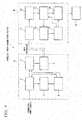
- a power-receiving device R related to the first embodiment constitutes a portion of a wireless power-transmitting system.
- the wireless power-transmitting system as shown in Figs. 1 and 2 , is constituted by a power-transmission device S and the power-receiving device R.
- the power-transmission device S is constituted of a power-transmission side power converter 1, an inverter circuit 2, a power-transmission side pad 3, a power-transmission side current/voltage sensor 4, a power-transmission side communication unit 5, and a power-transmission side control unit 6.
- the power-receiving device R is constituted of a power-receiving side pad 11, a power-receiving side power converter 12, a load circuit 13, a switch 14, a power-receiving side current/voltage sensor 15, a power-receiving side communication unit 16, and a power-receiving side control unit 17.
- the power-transmission device S is a device that is fixed and arranged in a power-transmission facility provided on the ground and wirelessly supplies AC power to the power-receiving device R provided at a movable body.
- the power-transmission facility is a facility in which a single vehicle stop space for the movable body or a plurality of vehicle stop spaces for the movable body are provided, and includes power-transmission devices S equivalent to the number of vehicle stop spaces.
- the power-receiving device R is a device that is provided in the movable body and charges a battery B (load device) by converting the AC power supplied from the power-transmission device S into DC power.
- the movable body is, for example, a vehicle, such as an electric car or a hybrid car, which requires the power reception from the outside.
- the power-transmission side power converter 1 is constituted of a power-transmission side rectifier circuit 1a and a chopper circuit 1b.
- the power-transmission side rectifier circuit 1a is, for example, a diode bridge, and performs full-wave rectification of the commercial power (for example, single-phase 100 v, 50 Hz) supplied from an external commercial power source, and outputs the full-wave rectified power to the chopper circuit 1b.
- the power (full-wave rectified power) supplied to the chopper circuit 1b from the power-transmission side rectifier circuit 1a is a monopolar (for example, positive polarity) pulsating current in which commercial sinusoidal power is folded at a zero cross point.
- the chopper circuit 1b adjusts its output voltage to output the adjusted output to the inverter circuit 2 by the switching operation thereof being controlled by the power-transmisson-side control unit 6.
- the chopper circuit 1b is a step-up chopper circuit or a step-up/down chopper circuit, and steps up and down the power input from the power-transmission side rectifier circuit 1a to output the stepped-up/down power.
- the output of the chopper circuit 1b is DC power obtained by full-wave rectified power that is a pulsating current being sufficiently smoothed by virtue of the function of a capacitor provided at an output terminal of the chopper circuit 1b.
- the chopper circuit 1b also functions as a power factor correction (PFC) circuit by the switching operation thereof being controlled by the power-transmission side control unit 6. That is, the chopper circuit 1b extends the conduction interval of the current of the full-wave rectified power to correct a power factor by switching the full-wave rectified power on the basis of the zero cross point of the full-wave rectified power at a frequency sufficiently higher than the frequency of the full-wave rectified power.
- PFC power factor correction
- the inverter circuit 2 is a power converter circuit that converts the DC power supplied from the power-transmission side rectifier circuit 1a of the power-transmission side power converter 1 into AC power of a predetermined frequency (driving frequency), on the basis of a switching signal (inverter-driving signal) input from the power-transmission side control unit 6. That is, the inverter circuit 2 converts DC power into AC power at a driving frequency by driving a plurality of switching elements using the above inverter-driving signal. Such an inverter circuit 2 outputs the AC power to the power-transmission side pad 3.
- the power-transmission side pad 3 is a circuit having a power-transmission coil 3a and a power-feeding capacitor.
- the power-transmission coil 3a of the power-transmission coil 3a and the power-feeding capacitor is provided at a position that faces a predetermined place (a place where the power-receiving coil 11a is provided) of the movable body that has stopped at the vehicle stop space.
- the power-transmission side current/voltage sensor 4 detects power feeding status information (information (value) on both or any one of a current and a voltage) of the power supplied from the commercial power source to the power-transmission side rectifier circuit 1a, and outputs detection signals showing the detected current and voltage to the power-transmission side control unit 6.
- the current sensor for example, a sensor that measures a magnetic field generated around an electric wire through which a current passes, due to the Hall effect, or a sensor that has a resistor inserted into an electric wire through which a current passes and measures a voltage drop that occurs in the resistor can be used.
- the voltage sensor for example, there is a sensor that divides a voltage by a resistance and converts the divided voltages into digital values using an analog-to-digital (AD) converter.
- AD analog-to-digital
- the power-transmission side communication unit 5 performs short-distance wireless communication with the power-receiving side communication unit 16 of the power-receiving device R.
- a communication method between the power-transmission side communication unit 5 and the power-receiving side communication unit 16 is short-distance wireless communication, such as ZigBee (registered trademark) or Bluetooth (registered trademark), or short-distance optical communication using light signals.
- the power-transmission side communication unit 5 has an antenna in the case of the communication method using electric waves, and has a light-receiving element for communication in the case of the communication method using the light signals.
- the power-transmission side control unit 6 is constituted of a central processing unit (CPU), a read-only memory (ROM), a random access memory (RAM), respective parts that are electrically connected to each other, an interface circuit that performs transmission and reception of various signals, and the like.
- the power-transmission side control unit 6 controls the overall operation of the power-transmission device S by performing various kinds of calculation processing on the basis of various calculation control programs stored in the above ROM, and performing communication with the respective parts. In addition, the details of the operation of the power-transmission side control unit 6 will be described below.
- the power-receiving side pad 11 is a circuit having a power-receiving coil 11a and a power-receiving capacitor.
- the power-receiving coil 11a is provided in a bottom part, a side part, an upper part, or the like of the movable body, and in a case where the movable body has stopped at a vehicle stop space, the power-receiving coil 11a faces in proximity the power-transmission coil 3a that constitutes the power-transmission device S.
- the power-receiving coil 11a faces in proximity the power-transmission coil 3a that constitutes the power-transmission side pad 3 and the power-receiving coil 11a is magnetically coupled to the power-transmission coil 3a. That is, the power-receiving side pad 11 wirelessly receives the AC power supplied to the power-transmission coil 3a by the inverter circuit 2 and the AC power according to the coupling coefficient of the power-transmission coil 3a and the power-receiving coil 11a from the power-transmission side pad 3, and outputs the received AC powers to the power-receiving side rectifier circuit 12a. That is, the wireless power-transmitting system is a wireless power-transmitting system based on a magnetic field resonance method, an electromagnetic induction method, or the like.
- the power-receiving side power converter 12 converts the power received from the power-transmission side pad 3 of the power-transmission device S via the power-receiving side pad 11 into power to be supplied to the battery B. Additionally, the power-receiving side power converter 12 is constituted of the power-receiving side rectifier circuit 12a and a filter circuit 12b.
- the power-receiving side rectifier circuit 12a is constituted of, for example, a diode bridge, and performs full-wave rectification of the AC power (received power) supplied from the power-receiving side pad 11 to output rectified AC power to the filter circuit 12b.
- the power supplied from the power-receiving side rectifier circuit 12a to the filter circuit 12b is full-wave rectified power subjected to full-wave rectification by the diode bridge.
- the filter circuit 12b is constituted of, for example, a reactor and a capacitor, and removes noise from the full-wave rectified power supplied from the power-receiving side control unit 17 and smoothens the power to output the smoothened power to the battery B.
- the reactor is, for example, a variable reactor.
- the load circuit 13 is provided between the filter circuit 12b and the switch 14, and is constituted of, for example, a resistor 13a and a switching element 13b.
- the switching element 13b is switched between an ON state (connected/closed state) and an OFF state (disconnected/open state) on the basis of control using the power-receiving side control unit 17.
- the switching element 13b includes, for example, an insulated gate bipolar transistor (IGBT), a bipolar transistor, a metal oxide semiconductor field-effect transistor (MOSFET), or the like. In a case where the switching element 13b is in the ON state, the power supplied wirelessly from the power-transmission device S is supplied to the resistor 13a.
- the DC power output from the filter circuit 12b is supplied to the resistor 13a.
- the switching element 13b is brought into the ON state when the switch 14 to be described below is in an OFF state.
- the resistance value of the resistor 13a be higher than the rated impedance of the battery B. This is because the power consumed by the resistor 13a can be reduced, and therefore, the resistor 13a can be downsized.
- the rated impedance is the range of impedance that can be taken in a desired use situation of the battery B. For example, in a case where the voltage of the battery B is 300 [V] and the desired amount of power supply is 3 [kW], a current of 10 [A] flows to the battery B.
- the impedance of the battery B reaches 30 [ ⁇ ]. Since the voltage of the battery B varies in a state of charge (SOC), the impedance of the battery B also varies in accordance with that variation. In a case where desired power is supplied to the battery B, the range of the impedance of the battery B that can be obtained is rated impedance.
- SOC state of charge
- the switch 14 is provided between the load circuit 13 and the battery B, and performs switching between an ON state and the OFF state on the basis of control using the power-receiving side control unit 17.
- the switch 14 is, for example, a switch, an electromagnetic contactor, a breaker, or the like, having a function of opening and closing a circuit, and switches between connection and disconnection between the load circuit 13 and the battery B.
- the switch 14 is provided, for example, in order to prevent an overcurrent and overvoltage of the battery B. When the switch 14 is brought into the OFF state, connection of the power-receiving device R with the battery B is released.
- the power-receiving side current/voltage sensor 15 detects the current and voltage of DC power that is supplied from the filter circuit 12b to the load circuit 13, and outputs the detection signals showing the detected current and voltage to the power-receiving side control unit 17.
- the current sensor for example, a sensor that measures a magnetic field generated around an electric wire through which a current passes, due to the Hall effect, or a sensor that has a resistor inserted into an electric wire through which a current passes and measures a voltage drop that occurs in the resistor can be used.
- the voltage sensor for example, there is a sensor that divides a voltage by a resistance and converts the divided voltages into digital values using an AD converter.
- the power-receiving side communication unit 16 performs short-distance wireless communication with the power-transmission side communication unit 5 of the power-transmission device S.
- a communication method between the power-transmission side communication unit 5 and the power-receiving side communication unit 16 is short-distance wireless communication, such as ZigBee (registered trademark) or Bluetooth (registered trademark), or short-distance optical communication using light signals.
- the power-receiving side communication unit 16 has an antenna in the case of the communication method using electric waves, and has a light-emitting element for communication in the case of the communication method using the light signals.
- the power-receiving side control unit 17 is constituted of a central processing unit (CPU), a read-only memory (ROM), a random access memory (RAM), respective parts that are electrically connected to each other, an interface circuit that performs transmission and reception of various signals, and the like.
- the power-receiving side control unit 17 controls the overall operation of the power-receiving device R by performing various kinds of calculation processing on the basis of various calculation control programs stored in the above ROM, and performing communication with the respective parts. In addition, the details of the operation of the power-receiving side control unit 17 will be described below.
- the battery B is a secondary battery, such as a lithium ion battery, or a nickel hydrogen secondary battery, and charges and stores the DC power supplied from the power-receiving side rectifier circuit 12a.
- the battery B is connected to an inverter (inverter for traveling) that drives a traveling motor of the movable body and/or a control device that controls the traveling of the movable body, and supplies driving power to the inverter for traveling and/or the control device.
- the power-receiving side control unit 17 of the power-receiving device R of the movable body brings the switching element 13b of the switch 14 and the load circuit 13 into an OFF state, when power is not transmitted (for example, at the time of the normal operation of the movable body by a driver).
- the power-transmission side control unit 6 of the power-transmission device S stops the chopper circuit 1b and the inverter circuit 2 when power is not transmitted, that is, when the movable body that is a power-transmission target does not stop at a stopping-and-parking position.
- a driver operates the movable body having the power-receiving device R, moves the power-receiving device R to an installation location for the power-transmission device S, and stops the movable body in that location.
- the power-receiving side control unit 17 of the power-receiving device R grasps an installation position for the power-transmission device S from the output of a position sensor, such as a sound wave sensor or an optical sensor that is not shown.
- the power-receiving side control unit 17 brings the switch 14 into the ON state from the OFF state if it is detected that the power-receiving device R has moved until the power-receiving device R faces the power-transmission device S based on the output of the position sensor, such as a sound wave sensor or an optical sensor, as described above.
- the position sensor such as a sound wave sensor or an optical sensor
- the power-transmission side control unit 6 of the power-transmission device S grasps the position of the power-receiving device R on the basis of the output of a position sensor, such as a sound wave sensor or an optical sensor that is not shown, similar to the power-receiving device R.
- the power-transmission side control unit 6 drives the chopper circuit 1b and the inverter circuit 2 if it is detected that the power-receiving device R has moved until the power-receiving device R faces the power-transmission device S above the power-transmission device S on the basis of the output of the position sensor, such as a sound wave sensor or an optical sensor, and makes the chopper circuit 1b and the inverter circuit 2 start a power transmission operation.
- the power-receiving side control unit 17 of the power-receiving device R determines an overvoltage or an overcurrent to the battery B, on the basis of a detection signal input from the power-receiving side current/voltage sensor 15.
- the power-receiving side control unit 17 brings the switch 14 into the OFF state from the ON state in order to protect the battery B in a case where it is determined that an overvoltage or an overcurrent to the battery B is generated Subsequently, the power-receiving side control unit 17 makes the power-receiving side communication unit 16 transmit a power transmission stop request, and brings the switching element 13b into the ON state.
- the state of the switch 14 is not limited to being switched on the grounds of an overvoltage or an overcurrent, and may be switched on the grounds of, for example, the temperature rise of the battery B.
- the power-transmission side control unit 6 If the power-transmission side control unit 6 receives the power transmission stop request from the power-receiving device R, the power-transmission side communication unit 5 of the power-transmission device S stops the driving of the chopper circuit 1b and the inverter circuit 2 to make the chopper circuit 1b and the inverter circuit 2 stop the power transmission operation.
- the switching element 13b is brought into the ON state when the power-receiving side communication unit 16 is made to transmit a power transmission stop request. Therefore, the power from the power-transmission device S is supplied to the resistor 13a and consumed until transmission of power by the power-transmission device S is stopped.
- the voltage of the power-receiving side pad 11 or the power-receiving side power converter 12 of the power-receiving device R rises before power transmission is actually stopped after the power-receiving side communication unit 16 transmits a power transmission stop request (refer to FIG. 3 ).
- the switch 14 is in the OFF state, and therefore, the power supplied from the power-transmission device S to the power-receiving device R is not supplied to the battery B and is not consumed.
- the voltage of elements that constitute the power-receiving side pad 11 or the power-receiving side power converter 12 of the power-receiving device R rises and the elements are damaged.
- the resistor 13a has such a resistance value that prevents the voltage of the elements of the power-receiving side pad 11 or the power-receiving side power converter 12 docs not reach a breakdown voltage until a power transmission stop request is transmitted from the power-receiving device R to the power-transmission device S and power transmission is stopped.
- the resistance value of the resistor 13a is determined by the following method in a design stage or the like.
- the time before power transmission is stopped through the transmission of the power transmission stop request after the switch 14 is switched to the OFF state is calculated.
- a resistor having a resistance value considered not to reach the breakdown voltage of an element for example, an element with a lowest breakdown voltage
- the breakdown voltage of the element with the highest possibility of damage is exceeded within the calculated time.
- the resistance value is gradually raised, it is confirmed whether or not the breakdown voltage of the element with the highest possibility of damage is exceeded within the calculated time, and the highest resistance value that does not exceed the breakdown voltage of the element with a high possibility of damage within the calculated time is derived. Since heat generation of the resistor 13a is suppressed as the resistance value thereof becomes higher, surface area can be made small. That is, the resistor 13a can be made smaller as the resistance value thereof becomes higher.
- the power-receiving side control unit 17 may determine whether or not the switching element 13b is brought into the ON state on the basis of the detection signal input from the power-receiving side current/voltage sensor 15. That is, the power-receiving side control unit 17 brings the switching element 13b into the ON state in a case where a voltage detected by the power-receiving side current/voltage sensor 15 rises and exceeds a threshold value when the switch 14 is brought into the OFF state from the ON state at the time of power transmission (refer to FIG. 3 ). In this case, the power-receiving side control unit 17 makes the power-receiving side communication unit 16 transmit a power transmission stop request, similar to the above operation.
- the power-receiving device R includes the load circuit 13 constituted of the resistor 13a and the switching element 13b that are connected in series between a pair of output terminals of the power-receiving side power converter 12.
- the switching element 13b is switched from the disconnected state to the connected state if the power-receiving device R and the battery B are disconnected from each other.
- the resistor 13a has such a resistance value that the voltage of the elements of the power-receiving side pad 11 or the power-receiving side power converter 12 does not reach the breakdown voltage before the power-transmission device S stops power transmission to the power-receiving device R after the power-receiving device R and the battery B are disconnected from each other. Accordingly, damage to the elements in the power-receiving device R can be prevented.
- the wireless power-transmitting system related to the second embodiment is constituted by the power-transmission device S and the power-receiving device R. Additionally, as shown, the power-transmission device S is constituted of the power-transmission side power converter 1, the inverter circuit 2, the power-transmission side pad 3, the power-transmission side current/voltage sensor 4 (detecting unit), and the power-transmission side control unit 6.
- the power-receiving device R is constituted of the power-receiving side pad 11, the power-receiving side power converter 12, the load circuit 13, the switch 14, the power-receiving side current/voltage sensor 15, and the power-receiving side control unit 17.
- the power-receiving side control unit 17 of the power-receiving device R in the second embodiment determines an overvoltage or an overcurrent to the battery B, on the basis of the detection signal input from the power-receiving side current/voltage sensor 15.
- the power-receiving side control unit 17 brings the switch 14 into the OFF state from the ON state in order to protect the battery B in a case where it is determined that an overvoltage or an overcurrent to the battery B is generated. Subsequently, the power-receiving side control unit 17 brings the switching element 13b into the ON state.
- the state of the switch 14 is not limited to being switched on the grounds of an overvoltage or an overcurrent, and may be switched on the grounds of, for example, the temperature rise of the battery B.
- the opening of the switch 14 may be not only intentionally performed by the power-receiving side control unit 17 but also unintentionally performed depending on the malfunction of the switch 14, or the like.
- the power-transmission side control unit 6 of the power-transmission device S determines whether or not a current (power transmission status information) exceeds a threshold value on the basis of a detection signal input from the power-transmission side current/voltage sensor 4. That is, in the wireless power-transmitting system, the switch 14 of the power-receiving device R is brought into the OFF stage, the switching element 13b is brought into the ON state, and the resistor 13a is connected to the power-receiving side power converter 12. That is, the power transmitted wirelessly from the power-transmission device S is supplied to the resistor 13a. Accordingly, a change in impedance occurs in the power-receiving device R. A current detected by the power-transmission side current/voltage sensor 4 of the power-transmission device S also changes with the change in impedance. The power-transmission side control unit 6 detects the change in current.
- the power-transmission side control unit 6 determines that the current exceeds the threshold value on the basis of the detection signal input from the power-transmission side current/voltage sensor 4, the power-transmission side control unit 6 stops the driving of the chopper circuit 1b and the inverter circuit 2, and makes the chopper circuit 1b and the inverter circuit 2 stop the power transmission operation.
- the power-transmission side control unit 6 may obtain power from information on the current and the voltage (power transmission status information) obtained from the power-transmission side current/voltage sensor 4, and may stop the driving of the chopper circuit 1b and the inverter circuit 2 on the basis of the power. That is, if the power-transmission side control unit 6 determines that the power based on the detection signal input from the power-transmission side current/voltage sensor 4 exceeds the threshold value, the driving of the chopper circuit 1b and the inverter circuit 2 may be stopped.
- the power-transmission side control unit 6 may use a voltage instead of the current, as a determination target. That is, if the power-transmission side control unit 6 determines that the power (power transmission status information) exceeds the threshold value on the basis of the detection signal input from the power-transmission side current/voltage sensor 4, the driving of the chopper circuit 1b and the inverter circuit 2 may be stopped.
- the switching element 13b is brought into the ON state when the switch 14 is brought into the OFF state, the power from the power-transmission device S is supplied to the resistor 13a and consumed until transmission of power by the power-transmission device S is stopped.
- the voltage of the power-transmission side power converter 1, the inverter circuit 2, or the power-transmission side pad 3 of the power-transmission device S or the voltage of the power-receiving side pad 11 or the power-receiving side power converter 12 of the power-receiving device R rises until the switch 14 is brought into the OFF state and power transmission is actually stopped (refer to FIG. 6 ). This is because the switch 14 is in the OFF state, and therefore, the power supplied from the power-transmission device S to the power-receiving device R is not supplied to the battery B and is not consumed.
- the voltage of elements that constitute the power-transmission side power converter 1, the inverter circuit 2, or the power-transmission side pad 3 of the power-transmission device S or the power-receiving side pad 11 or the power-receiving side power converter 12 of the power-receiving device R rises, and if the voltage exceeds an element damage level, the elements are damaged.
- the resistor 13a has such a resistance value that the voltage of the internal elements in the power-transmission device S and the power-receiving device R does not reach a breakdown voltage before the transmission of power to the power-receiving device R by the power-transmission device S is stopped after the switch 14 is brought into the OFF state.
- the resistance value of the resistor 13a is determined by the following method in a design stage or the like.
- the time until the switch 14 is switched to the OFF state and power transmission is stopped is calculated.
- the resistor 13a having a resistance value considered not to reach the breakdown voltage of an element (for example, an element with a lowest breakdown voltage) with a highest possibility of damage in the power-transmission side power converter 1, the inverter circuit 2, or the power-transmission side pad 3 of the power-transmission device S or the power-receiving side pad 11 or the power-receiving side power converter 12 of the power-receiving device R is provided, and it is confirmed whether or not the breakdown voltage of the element with the highest possibility of damage is exceeded within the calculated time.
- the resistance value is gradually raised, it is confirmed whether or not the breakdown voltage of the element with the highest possibility of damage is exceeded within the calculated time, and the highest resistance value that does not exceed the breakdown voltage of the element with the highest possibility of damage within the calculated time is derived. Since heat generation of the resistor 13a is suppressed as the resistance value thereof becomes higher, surface area can be made small. That is, the resistor 13a can be made smaller as the resistance value thereof becomes higher.
- the power-receiving side control unit 17 may determine whether or not the switching element 13b is brought into the ON state on the basis of the detection signal input from the power-receiving side current/voltage sensor 15. That is, the power-receiving side control unit 17 brings the switching element 13b into the ON state in a case where the voltage detected by the power-receiving side current/voltage sensor 15 rises and exceeds a threshold value when the switch 14 is brought into the OFF state from the ON state at the time of power transmission (refer to FIG. 6 ).
- the switching element 13b is brought into the ON state, and consequently, an output voltage drawn as a first example of the second embodiment shown in FIG. 6 rises more gently than in the related art, the output voltage continues rising until power transmission stops.
- the switching element 13b is brought into the ON state, and consequently, an output voltage drawn as a second example of the second embodiment shown in FIG. 6 rises gently. If the output voltage rises up to a certain voltage, the rise thereof stops and the output voltage is brought into a stable state.
- a difference between the changes of the output voltages in the first example and the second example of the second embodiment is caused depending on a difference between the resistance values of the resistors 13a.
- the timing of power transmission stop varies depending on the threshold value that is used in order for the power-transmission side control unit 6 to detect a change in a current, a voltage, or power.
- the threshold value depending on the threshold value, power transmission may be stopped before the switching element 13b is brought into the ON state, and power transmission may be stopped after the switching element 13b is brought into the ON state.
- the threshold value in a case when power transmission is stopped before the switching element 13b is brought into the ON state is a low value compared to the threshold value in a case where power transmission is stopped after the switching element 13b is brought into the ON state.
- the switching element 13b of the load circuit 13 is brought into the ON state. Accordingly, a change in impedance occurs in the power-receiving device R. A current detected by the power-transmission side current/voltage sensor 4 of the power-transmission device S also changes with the change in impedance. Then, if the power-transmission side control unit 6 of the power-transmission device S determines that the current exceeds the threshold value on the basis of the detection signal input from the power-transmission side current/voltage sensor 4, power transmission to the power-receiving device R is stopped.
- the power-receiving device R since the power-transmission device S determines the stop of power transmission, the power-receiving device R does not need to transmit a power feeding stop request to the power-transmission device S. Therefore, due to the time delay of communication between the power-receiving device R and the power-transmission device S, the voltage of the elements of the power-transmission device S or the power-receiving device R does not rise, and these elements are not damaged.
- the switching element 13b of the load circuit 13 is brought into the ON state. Accordingly, the power from the power-transmission device S is consumed by the resistor 13a. Therefore, a rise in spontaneous voltage caused by the opening of the switch 14 is suppressed, and damage to the elements of the power-receiving device R or the power-transmission device S can be prevented before power transmission is stopped after the switch 14 is brought into the open state.
- the load circuit 13 is provided in the subsequent stage of the power-receiving side power converter 12. That is, by providing the load circuit 13 in the preceding stage of the power-receiving side power converter 12, the power consumed by the resistor 13a does not become AC power, but the power consumed by the resistor 13a becomes DC power. In this way, in the second embodiment, by making the power consumed by the resistor 13a as DC power, it is possible to avoid that heat generation increases under the influence of a skin effect in a case where the power consumed by the resistor 13a is AC power. Additionally, according to the second embodiment, a change in the resistance value of the resistor 13a caused by heat can be suppressed by avoiding the increase of heat generation.
- the power sensor for example, a voltage and a current are measured by a voltage sensor and a current sensor, and a sensor averages a value, which is obtained by multiplying the voltage and the current, with time, thereby obtaining power. In this case, the power transmission status information becomes power.
- the power-receiving device According to the power-receiving device, the wireless power-transmitting system, and the power-transmission device of this disclosure, damage to the elements can be prevented.
Landscapes
- Engineering & Computer Science (AREA)
- Power Engineering (AREA)
- Computer Networks & Wireless Communication (AREA)
- Transportation (AREA)
- Mechanical Engineering (AREA)
- Charge And Discharge Circuits For Batteries Or The Like (AREA)
Applications Claiming Priority (3)
| Application Number | Priority Date | Filing Date | Title |
|---|---|---|---|
| JP2014137880A JP2016015862A (ja) | 2014-07-03 | 2014-07-03 | 受電装置 |
| JP2014257201A JP2016119759A (ja) | 2014-12-19 | 2014-12-19 | 非接触給電システム及び送電装置 |
| PCT/JP2015/068981 WO2016002839A1 (ja) | 2014-07-03 | 2015-07-01 | 受電装置、非接触給電システム及び送電装置 |
Publications (2)
| Publication Number | Publication Date |
|---|---|
| EP3166203A1 true EP3166203A1 (de) | 2017-05-10 |
| EP3166203A4 EP3166203A4 (de) | 2018-01-03 |
Family
ID=55019369
Family Applications (1)
| Application Number | Title | Priority Date | Filing Date |
|---|---|---|---|
| EP15814891.6A Withdrawn EP3166203A4 (de) | 2014-07-03 | 2015-07-01 | Stromaufnahmevorrichtung, kontaktloses stromversorgungssystem und stromeinspeisungsvorrichtung |
Country Status (4)
| Country | Link |
|---|---|
| US (1) | US20170093225A1 (de) |
| EP (1) | EP3166203A4 (de) |
| CN (1) | CN106464018A (de) |
| WO (1) | WO2016002839A1 (de) |
Cited By (1)
| Publication number | Priority date | Publication date | Assignee | Title |
|---|---|---|---|---|
| US20220158500A1 (en) * | 2019-04-26 | 2022-05-19 | Mitsubishi Electric Corporation | Elevator |
Families Citing this family (21)
| Publication number | Priority date | Publication date | Assignee | Title |
|---|---|---|---|---|
| EP3748812A1 (de) | 2016-02-03 | 2020-12-09 | General Electric Company | Verfahren und system zum schutz eines systems zur drahtlosen stromübertragung |
| SG10201700633QA (en) | 2016-02-03 | 2017-09-28 | Gen Electric | System and method for protecting a wireless power transfer system |
| JP6642119B2 (ja) * | 2016-03-02 | 2020-02-05 | オムロン株式会社 | 充電器 |
| SG10201707385XA (en) | 2016-09-30 | 2018-04-27 | Gen Electric | Over voltage protection for a wireless power transfer system |
| US10291075B2 (en) * | 2017-02-22 | 2019-05-14 | Qualcomm Incorporated | Over voltage protection detection |
| EP3462564A4 (de) * | 2017-04-07 | 2019-05-08 | Guangdong Oppo Mobile Telecommunications Corp., Ltd. | Drahtloses ladesystem, vorrichtung und verfahren sowie aufzuladende vorrichtung |
| CN109417308B (zh) | 2017-04-07 | 2023-06-20 | Oppo广东移动通信有限公司 | 无线充电系统、装置、方法及待充电设备 |
| WO2019039946A1 (en) * | 2017-08-25 | 2019-02-28 | Apple Inc. | WIRELESS POWER TRANSFER CONTROL |
| US11075515B2 (en) * | 2018-06-05 | 2021-07-27 | Nuvolta Technologies (Hefei) Co., Ltd. | Overvoltage protection device and method thereof |
| WO2020049853A1 (ja) * | 2018-09-05 | 2020-03-12 | 三菱電機株式会社 | 非接触給電システムおよび送電装置 |
| US10892800B1 (en) | 2020-01-06 | 2021-01-12 | Nucurrent, Inc. | Systems and methods for wireless power transfer including pulse width encoded data communications |
| US11303164B2 (en) | 2020-07-24 | 2022-04-12 | Nucurrent, Inc. | Low cost communications demodulation for wireless power transmission system |
| US11303165B2 (en) | 2020-07-24 | 2022-04-12 | Nucurrent, Inc. | Low cost communications demodulation for wireless power receiver system |
| US11431204B2 (en) | 2021-02-01 | 2022-08-30 | Nucurrent, Inc. | Automatic gain control for communications demodulation in wireless power transfer systems |
| US11277035B1 (en) | 2021-02-01 | 2022-03-15 | Nucurrent, Inc. | Automatic gain control for communications demodulation in wireless power transmitters |
| US11431205B2 (en) | 2021-02-01 | 2022-08-30 | Nucurrent, Inc. | Systems and methods for receiver beaconing in wireless power systems |
| US11277031B1 (en) | 2021-02-01 | 2022-03-15 | Nucurrent, Inc. | Automatic gain control for communications demodulation in wireless power transmitters |
| US11277034B1 (en) | 2021-02-01 | 2022-03-15 | Nucurrent, Inc. | Systems and methods for receiver beaconing in wireless power systems |
| US11811244B2 (en) * | 2021-02-01 | 2023-11-07 | Nucurrent, Inc. | Automatic gain control for communications demodulation in wireless power transmitters |
| US11569694B2 (en) | 2021-02-01 | 2023-01-31 | Nucurrent, Inc. | Automatic gain control for communications demodulation in wireless power receivers |
| JP7605173B2 (ja) * | 2022-04-12 | 2024-12-24 | トヨタ自動車株式会社 | 制御装置、制御方法、プログラム、非接触電力伝送システム |
Family Cites Families (15)
| Publication number | Priority date | Publication date | Assignee | Title |
|---|---|---|---|---|
| GB2414120B (en) * | 2004-05-11 | 2008-04-02 | Splashpower Ltd | Controlling inductive power transfer systems |
| US8004235B2 (en) * | 2006-09-29 | 2011-08-23 | Access Business Group International Llc | System and method for inductively charging a battery |
| JP2011114985A (ja) * | 2009-11-27 | 2011-06-09 | Sanyo Electric Co Ltd | 電池内蔵機器と充電台 |
| KR20120120330A (ko) * | 2010-01-29 | 2012-11-01 | 가부시키가이샤 한도오따이 에네루기 켄큐쇼 | 반도체 장치 |
| US8830637B2 (en) * | 2010-08-31 | 2014-09-09 | Texas Instruments Incorporated | Methods and apparatus to clamp overvoltages for alternating current systems |
| JP5703988B2 (ja) * | 2011-06-17 | 2015-04-22 | トヨタ自動車株式会社 | 受電装置、送電装置、車両、および非接触給電システム |
| JP2014187723A (ja) * | 2011-07-16 | 2014-10-02 | Sanyo Electric Co Ltd | 電池内蔵機器と充電台、及び電池内蔵機器 |
| JP2013102665A (ja) * | 2011-10-21 | 2013-05-23 | Sony Corp | 給電装置および給電システム |
| JP2013118719A (ja) * | 2011-12-01 | 2013-06-13 | Sanyo Electric Co Ltd | 充電台、電池駆動機器、充電システム及び充電方法 |
| JP2013225962A (ja) * | 2012-04-20 | 2013-10-31 | Panasonic Corp | 非接触電力伝送装置 |
| US9130369B2 (en) * | 2012-08-29 | 2015-09-08 | Qualcomm Incorporated | Wireless power overvoltage protection circuit with reduced power dissipation |
| JP6008672B2 (ja) * | 2012-09-26 | 2016-10-19 | ローム株式会社 | ワイヤレス受給電装置、ワイヤレス受電機器、およびワイヤレス給電機器 |
| JP5998905B2 (ja) * | 2012-12-14 | 2016-09-28 | Tdk株式会社 | ワイヤレス受電装置およびそれを用いたワイヤレス電力伝送装置 |
| DE102014219504B4 (de) * | 2014-09-26 | 2022-12-08 | Vitesco Technologies GmbH | Drahtloses Batterieladesystem mit Notabschaltung für eine Fahrbatterie eines Elektrofahrzeugs |
| EP3010129A1 (de) * | 2014-10-16 | 2016-04-20 | Nxp B.V. | Eingangsschaltungen für drahtlose Stromempfänger, drahtlose Ladegeräte und drahtloses Laden |
-
2015
- 2015-07-01 EP EP15814891.6A patent/EP3166203A4/de not_active Withdrawn
- 2015-07-01 CN CN201580030741.7A patent/CN106464018A/zh active Pending
- 2015-07-01 WO PCT/JP2015/068981 patent/WO2016002839A1/ja not_active Ceased
-
2016
- 2016-12-13 US US15/377,435 patent/US20170093225A1/en not_active Abandoned
Cited By (1)
| Publication number | Priority date | Publication date | Assignee | Title |
|---|---|---|---|---|
| US20220158500A1 (en) * | 2019-04-26 | 2022-05-19 | Mitsubishi Electric Corporation | Elevator |
Also Published As
| Publication number | Publication date |
|---|---|
| EP3166203A4 (de) | 2018-01-03 |
| US20170093225A1 (en) | 2017-03-30 |
| CN106464018A (zh) | 2017-02-22 |
| WO2016002839A1 (ja) | 2016-01-07 |
Similar Documents
| Publication | Publication Date | Title |
|---|---|---|
| EP3166203A1 (de) | Stromaufnahmevorrichtung, kontaktloses stromversorgungssystem und stromeinspeisungsvorrichtung | |
| US10305334B2 (en) | Wireless power-supplying system, power-receiving device, and power-transmitting device | |
| JP7659335B2 (ja) | ワイヤレス電力伝送のためのフェールセーフ安全回路 | |
| US10277082B2 (en) | Power-transmitting device and wireless power-supplying system | |
| JP7538289B2 (ja) | ワイヤレス電力伝送システムを保護するためのシステムおよび方法 | |
| EP3121932B1 (de) | Stromversorgungsvorrichtung und system zur kontaktlosen stromversorgung | |
| JP2016015862A (ja) | 受電装置 | |
| US9634636B2 (en) | Non-contact power transmission device | |
| JP7581422B2 (ja) | ワイヤレス電力伝送システムを保護するための方法およびシステム | |
| WO2015198895A1 (ja) | 送電機器及び非接触電力伝送装置 | |
| JP2016119759A (ja) | 非接触給電システム及び送電装置 | |
| CN107887984A (zh) | 用于无线电力传送系统的过电压保护 | |
| JP2014220940A (ja) | 非接触充電システムおよび非接触充電方法 | |
| CN104518548B (zh) | 电驱动车辆的充电站 | |
| JP2019115148A (ja) | 非接触受電装置 | |
| JP2015220853A (ja) | 非接触給電システム | |
| EP3131176A1 (de) | Energieübertragungsvorrichtung und kontaktfreies kraftübertragungsverfahren | |
| US20200389051A1 (en) | Non-contact power supply apparatus and non-contact power transmission system | |
| JP6425183B2 (ja) | 非接触給電装置および非接触給電システム | |
| JP2016019366A (ja) | 送電機器及び非接触電力伝送装置 | |
| JP2015104164A (ja) | 送電機器及び非接触電力伝送装置 | |
| JP2015231308A (ja) | 受電装置及び非接触給電システム | |
| CN116691381B (zh) | 车辆充电方法、车辆充电系统和车辆 |
Legal Events
| Date | Code | Title | Description |
|---|---|---|---|
| PUAI | Public reference made under article 153(3) epc to a published international application that has entered the european phase |
Free format text: ORIGINAL CODE: 0009012 |
|
| 17P | Request for examination filed |
Effective date: 20161213 |
|
| AK | Designated contracting states |
Kind code of ref document: A1 Designated state(s): AL AT BE BG CH CY CZ DE DK EE ES FI FR GB GR HR HU IE IS IT LI LT LU LV MC MK MT NL NO PL PT RO RS SE SI SK SM TR |
|
| AX | Request for extension of the european patent |
Extension state: BA ME |
|
| DAV | Request for validation of the european patent (deleted) | ||
| DAX | Request for extension of the european patent (deleted) | ||
| A4 | Supplementary search report drawn up and despatched |
Effective date: 20171130 |
|
| RIC1 | Information provided on ipc code assigned before grant |
Ipc: H02J 7/00 20060101ALN20171124BHEP Ipc: H02J 50/12 20160101AFI20171124BHEP Ipc: H02H 9/04 20060101ALI20171124BHEP Ipc: B60L 11/18 20060101ALI20171124BHEP Ipc: H02H 9/02 20060101ALN20171124BHEP Ipc: H02J 50/90 20160101ALN20171124BHEP Ipc: H02J 50/80 20160101ALN20171124BHEP Ipc: H02J 7/02 20160101ALI20171124BHEP |
|
| STAA | Information on the status of an ep patent application or granted ep patent |
Free format text: STATUS: THE APPLICATION IS DEEMED TO BE WITHDRAWN |
|
| 18D | Application deemed to be withdrawn |
Effective date: 20180703 |