EP3170010B1 - Dispositif et procédé de mesure de courant - Google Patents
Dispositif et procédé de mesure de courant Download PDFInfo
- Publication number
- EP3170010B1 EP3170010B1 EP15745147.7A EP15745147A EP3170010B1 EP 3170010 B1 EP3170010 B1 EP 3170010B1 EP 15745147 A EP15745147 A EP 15745147A EP 3170010 B1 EP3170010 B1 EP 3170010B1
- Authority
- EP
- European Patent Office
- Prior art keywords
- output
- current
- line
- feed
- inductive measurement
- Prior art date
- Legal status (The legal status is an assumption and is not a legal conclusion. Google has not performed a legal analysis and makes no representation as to the accuracy of the status listed.)
- Active
Links
Images


Classifications
-
- G—PHYSICS
- G01—MEASURING; TESTING
- G01R—MEASURING ELECTRIC VARIABLES; MEASURING MAGNETIC VARIABLES
- G01R19/00—Arrangements for measuring currents or voltages or for indicating presence or sign thereof
- G01R19/0092—Measuring current only
-
- H—ELECTRICITY
- H02—GENERATION; CONVERSION OR DISTRIBUTION OF ELECTRIC POWER
- H02M—APPARATUS FOR CONVERSION BETWEEN AC AND AC, BETWEEN AC AND DC, OR BETWEEN DC AND DC, AND FOR USE WITH MAINS OR SIMILAR POWER SUPPLY SYSTEMS; CONVERSION OF DC OR AC INPUT POWER INTO SURGE OUTPUT POWER; CONTROL OR REGULATION THEREOF
- H02M1/00—Details of apparatus for conversion
- H02M1/0003—Details of control, feedback or regulation circuits
- H02M1/0009—Devices or circuits for detecting current in a converter
Definitions
- the present invention relates to a method and an associated device for measuring load currents which are delivered to a consumer by an electrical supply device with two alternately switched power stages.
- German patent application DE 10 2009 046 255 A1 a half-bridge circuit, also called half-bridge arrangements.
- Such supply devices can be used in various applications, such as, for example, with switched-mode power supply units, inverters or drive inverters in an at least partially electrically driven vehicle, that is to say a hybrid vehicle, an electric vehicle or the like.
- the associated power stages usually have power semiconductors that work as switching elements. These are supplied by a suitable voltage source, which emits electrical power, and controlled by suitable driver stages, such as gate drivers.
- Electrical supply devices of the type mentioned emit a current - also called load current in the following - which can contain both a direct current component and an alternating current component. It is necessary for various applications to determine the value of the load current, for example to regulate this current, to display the operating status for a user of the associated system, etc.
- German patent application DE 101 07 791 A1 describes the use of coils, such as cylinder coils and Rogowski coils, in the context of power electronics.
- the solution described there has the disadvantages that special sample and hold electronics are necessary and complicated timing must be adhered to, which makes adaptation to the respective power semiconductor necessary.
- the d German Offenlegungsschrift DE 10 2012 210 261 A1 describes a power semiconductor module and a method for its operation.
- a half-bridge circuit is specifically described there, with various coils being provided to determine the load currents.
- the first of these coils are located directly next to a load current conductor or a load current conductor of a first power semiconductor switch.
- the second of these coils are located directly next to a second load current conductor or a second load current conductor of a second power semiconductor switch.
- the signals from the first coils and the signals from the second coils are fed to associated integrators and then evaluated accordingly.
- the U.S. Patent 5,815,391 relates to an invention for measuring the inverter current in a driver with pulse width modulation (PWM) for controlling a motor without using a Hall sensor.
- Rogowski coils can also be arranged in the area of the input lines or the output lines of the two inverter switches of the mentioned driver. Each of these coils is connected to an integrator. Both integrators each have a reset stage which keeps the output signal of the associated integrator at zero during the off time of the associated PWM signal for the associated inverter switch.
- a summation amplifier is also required.
- the object of the present invention is to implement a device - as well as a corresponding method - with which a load current that is emitted by a supply device of the type mentioned above can be determined in a simple and reliable manner.
- the invention is based on the following findings.
- Electrical supply devices of the type mentioned above such as in particular half-bridge circuits, contain two power stages, at least one of which can be controlled periodically by a driver, whereby they are usually switched on and off periodically.
- the switch-on period can be the same as the switch-off period. Usually, however, the switch-on period has a different duration than the switch-off period.
- Both power levels are switched on and off alternately. This means that if one of the levels is switched on, the other level is switched off. When one of these stages is switched on, it becomes conductive, so that a current can flow due to an applied voltage that is provided by a suitable power source. When this stage is switched off, this current flow is interrupted. However, these switching processes take place at a finite rate of current change (di / dt), the rates of current change being essentially the same at the switching times.
- a first inductive sensor is arranged in the area of a first feed line via which the first of the two power stages is supplied by the current source.
- a second inductive sensor in the area of a second feed line, via which the second of the two power levels is supplied from the power source.
- Sensors are each arranged with respect to their associated line in such a way that an appropriate voltage is induced with a corresponding current flow, which voltage is also particularly dependent on the dimensions and the geometry of the sensors. It is also possible for more than one inductive sensor to be arranged in the area of the first feed line and / or in the area of the second feed line, which are connected in a suitable manner.
- a load current flowing through one of the power stages can be measured both in the area of the aforementioned feed lines, which are usually directly or indirectly connected to a voltage or current source, and in the area of the output lines of the power stages. These output lines are usually connected together directly or indirectly and supply a consumer (load) that is to be supplied with the desired power current.
- the present invention therefore allows first inductive sensors to be arranged in the area of the feed lines and / or in the area of the output lines of the first of the aforementioned power stages. The same applies to the second of the inductive sensors that are used to measure the current in the second power stage.
- the first inductive sensors and the second inductive sensors are connected in series.
- the integrated sensor signals are read out at specified times within the switching periods. This readout can take place once or several times during a switch-on period and / or once or several times during a switch-off period. In a preferred embodiment, the reading takes place only once per switch-on period and once per switch-off period. It has proven particularly useful if this takes place essentially in the middle of each switching period, it being pointed out again that the switch-on period can have a different duration than the switch-off period.
- the aforementioned reading out of the integrated sensor signals at predetermined times leads to a series of measured values.
- a value for the load current which is output by the supply device and which usually has a direct current and an alternating current component.
- the output signal (or the output signals) can be used to feed it directly to further control stages. It is additionally or instead also possible that optical signals - such as the display of alphanumeric characters, bar graphs or the like - and / or acoustic signals - such as signal tones with different frequencies and / or volume, voice output or the like - are generated that give a user a hint on the operating status of the device.
- optical signals - such as the display of alphanumeric characters, bar graphs or the like - and / or acoustic signals - such as signal tones with different frequencies and / or volume, voice output or the like - are generated that give a user a hint on the operating status of the device.
- the invention is particularly inexpensive and reliable, both in production and in operation, if at least one of the inductive sensors is arranged directly on a circuit board. Other components can also be located on this.
- the circuit board can also have an opening (or several) around which at least one of the inductive measuring sensors is arranged as a metallic element and through which at least one of the above-mentioned lines of the power stages runs. It has proven particularly useful to use a circuit board with a double-sided metal layer, both metal layers being structured according to an associated layout and thereby realizing at least one of the inductive measuring sensors. It is of course also possible for both of these power supply lines to each run through an opening and for an associated inductive sensor to be arranged in the area of each of these openings.
- Fig. 1 shows the basic circuit diagram of a half-bridge arrangement for supplying a consumer 10 with electrical power or a corresponding load current i L.
- the arrangement is fed by a voltage source 12 which emits a direct voltage U DC and to which a smoothing capacitor 14 is connected in parallel.
- the half-bridge arrangement has an upper stage 16a and a lower stage 16b.
- the upper stage 16a contains an upper switching transistor 18a and an associated upper freewheeling diode 20a and is connected to the positive pole of the voltage source 12 via a feed line 21a.
- the lower stage 16b contains a lower switching transistor 18b and an associated freewheeling diode 20b and is connected to the negative pole of the voltage source 12 via a feed line 21b.
- the output line 31a of the upper stage 16a and the output line 31b of the lower stage are connected together directly or indirectly and jointly supply the consumer 10 with the load current i L via the line 11.
- the switching transistors 18 can be designed in various ways, such as, for example, a MOS field effect transistor (MOSFET), a bipolar transistor with an insulated gate (IGBT), a bipolar transistor, a field effect transistor (FET), but also a gate turn-off thyristor (GTO). , as a thyristor or the like.
- the upper switching transistor 18a is controlled by an upper gate driver 22a via a control line 23a and the lower switching transistor 18b is controlled by a lower gate driver 22b via a control line 23b.
- a first input of each of these drivers 22 is each connected to an output of a control unit 24, which via it emits output signals sa1, sa2 to drivers 22a and 22b, respectively.
- Another output of the control unit 24 emits a further output signal sa3 to the input of a display unit 25 which is designed such that it can reproduce signals optically and / or acoustically.
- an input unit 27 is provided, via which control signals se can be fed to the control unit 24 by a user.
- Second inputs of the gate driver 22 are commonly connected to the output of a comparator 26.
- the input of this comparator 26 is connected to an input of the control unit 24 and to the output of an integrator 28, which is below with the help of Fig. 2 is described in more detail.
- the comparator 26 is shown in FIG Fig. 1 shown in greatly simplified form. In fact, it has a further input, which is not shown here and to which a fixed voltage value is specified as the overcurrent limit.
- it makes sense to provide two comparators, namely one for overcurrent detection in the positive direction and another for overcurrent detection in the negative direction. This circuit can serve as short-circuit or overcurrent detection and cause both driver circuits 22a and 22b to be safely switched off or locked, independently of the control device 24.
- the inputs 29a, 29b of the integrator 28 are connected to a Rogowski coil 30, which in this basic circuit diagram has an upper part 30a and a lower part 30b which are connected in series with one another.
- the load current i L generated by the stages 16a, 16b is fed to the consumer 10 via a line 11.
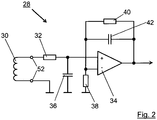
- Fig. 2 shows a preferred embodiment of the integrator 28.
- the Rogowski coil 30 At its input is the Rogowski coil 30, that is, the series connection of the two parts 30a and 30b.
- the coil 30 is connected via a resistor 32 on the one hand to a first input (+) of an operational amplifier 34 and on the other hand to a capacitor 36.
- the second input (-) of the operational amplifier 34 is on the one hand connected to ground via a further resistor 38.
- Another resistor 40 and a capacitor 42 connected in parallel thereto connect the second input (-) to the output of the operational amplifier 34.
- the output of the operational amplifier 34 - and thus of the integrator 28 - is connected to both the control unit 24 and the comparator 26 (sa Fig. 1 ).
- an analog signal is emitted via this output, which is digitized within the control unit 24 by an analog-digital converter (not shown here).
- the Rogowski coil 30 is implemented as an air core coil.
- the conductor of which is arranged on a circuit board that also accommodates other - or possibly all - of the electronic or electrical components from the circuits shown above.
- the Figures 3 - 5 show the basic layout 130 of the Rogowski coil 30, as it is implemented in the preferred embodiment on a double-sided board (not shown here). It shows Fig. 3 the layout 133 for one - for example the upper - side of the board and Fig. 4 shows the layout 134 for the other side of the board. In Fig. 5 the combination 135 of the two layouts mentioned is shown symbolically.
- the representation of the layouts 133, 134, 135 is each divided into a first part a and a second part b. This corresponds to the subdivision of the Rogowski coil 30, as in FIG Fig. 1 shown.
- the layout 133 represents the metal tracks on the top and the layout 134 the metal tracks on the underside of the circuit board. Such metal tracks usually consist of copper.
- these metal tracks run around a first opening 48 in the Figures 3 - 5 is shown on the left, and a second opening 50, which is shown on the right.
- These two openings 48, 50 can be produced within the board by suitable processing steps, such as milling, drilling, sawing, etching, punching and / or the like.
- the connections 52 serve to connect the Rogowski coil 30 to the integrator 28 (see also Fig Fig. 1 and 2 ).
- the line 21a also runs through the opening 48 and the line 21b through the opening 50.
- the upper stage 16a is fed with a current i 1 via the line 21a, the value of which is dependent on the activation of the upper switching transistor 18a by the Gate driver 22a.
- the lower stage 16b is fed via the line 21b with a current i 2 , the value of which is dependent on the activation of the switching transistor 18b by the gate driver 22b.
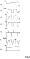
- the load current i L usually consists of a direct component, an alternating component and a certain ripple with the periodicity of the switching events, as in FIG Figure 6a shown.
- FIG Figure 6a Of particular interest is the course of the mean current values, which are shown in Figure 6a are shown in dashed lines.
- Such a current profile for i L arises when the switching transistors 18a and 18b are alternately switched on and off by the gate drivers 22a, 22b.
- Figure 6b shows an example of the associated course of the voltage u GS1 (see Fig Fig. 1 ) to control the upper switching transistor 18a.
- the current i 1 in the upper switching path 16a corresponds to the load current i L when the switching transistor 18a is on and zero when the switching transistor 18a is off.
- the switching operations take place with a finite di / dt.
- the associated course is in Figure 6c shown.
- the current i 2 in the lower switching path 16b corresponds - according to the above-mentioned formulas (2) or (1) - to the load current i L with the opposite Sign for conducting switching transistor 18b and zero for blocking switching transistor 18b (see Sect. Fig. 6d ).
- the Rogowski voltage U R which is delivered by the Rogowski coil 30 to the inputs 29a, 29b of the integrator 28, is proportional to the rate of current change ( Figure 6e ).
- ⁇ U R dt the course of the current in the intermediate circuit connections - line 21a or 21b - of the half bridge can be recovered, but without a direct current component.
- control unit 24 samples the output signal of the integrator 28 for the current measurement at predetermined times; namely to the pulse center of both switching states. These times are in Fig. 6f marked by arrows and they are known to the control unit 24, since it controls the control transistors 18a, 18b via the gate drivers 22a, 22b.
- the direct component of the load current i L can be determined, since the current in the respective blocking switching transistor 18 is always zero.
- the direct and alternating current components of the load current i L can therefore be determined by the difference between successive sampled values.
- Fig. 6g the associated measured values M are shown symbolically. To be precise, this results in the respective mean value of the load current i L within one pulse period of the switching pattern. This contains the direct current and the alternating current component of the load current i L , but not the high-frequency component with switching frequency, which is usually not of interest either.
- the circuit shown In addition to the measurement of the values for the current i L , which can be displayed optically and / or acoustically by means of the display unit 25, the circuit shown also allows a corresponding regulation with the aid of the control unit 24.
- an overcurrent limit can be specified. This can take place on the basis of a voltage with a predetermined value at the second connection (not shown here) of the comparator 26. However, it is additionally or instead also possible for a corresponding limit value to be fed to the control unit 24 by means of the input unit 27.
Landscapes
- Physics & Mathematics (AREA)
- General Physics & Mathematics (AREA)
- Measurement Of Current Or Voltage (AREA)
- Measuring Instrument Details And Bridges, And Automatic Balancing Devices (AREA)
Claims (15)
- Dispositif permettant de de terminer un courant de charge (iL) délivré par un équipement d'approvisionnement qui présente un premier étage de puissance (16a) et un deuxième étage de puissance (16b), dans lequel- le premier étage de puissance (16a) peut être alimenté par un premier courant d'alimentation (i1) par l'intermédiaire d'une première ligne d'alimentation (21a), et peut délivrer un premier courant de sortie par l'intermédiaire d'une première ligne de sortie (31a),- le deuxième étage de puissance (16b) peut être alimenté par un deuxième courant d'alimentation (i2) par l'intermédiaire d'une deuxième ligne d'alimentation (21b), et peut délivrer un deuxième courant de sortie par l'intermédiaire d'une deuxième ligne de sortie (31b),- les étages de puissance (16a, 16b) peuvent être commutés en alternance par une unité de commande (24), par l'intermédiaire d'une première ligne de commande (23a) ou par l'intermédiaire d'une deuxième ligne de commande (23b), pendant respectivement une période de commutation prédéfinie à variation de courant finie (di/dt) de sorte que les valeurs des courants d'alimentation (i1 ; i2) ou les valeurs des courants de sortie peuvent être influencées,- un premier capteur de mesure inductif (30a) est disposé au niveau de la première ligne d'alimentation (21a) et/ou au niveau de la première ligne de sortie (31a), et- un deuxième capteur de mesure inductif (30b) est disposé au niveau de la deuxième ligne d'alimentation (21b) et/ou au niveau de la deuxième ligne de sortie (31b),- au moins un intégrateur (28) est prévu qui est aménagé pour intégrer les signaux de capteur des capteurs de mesure inductifs (30a, 30b),- une unité de commande (24) est prévue qui est aménagée pour extraire les signaux de capteur intégrés à des instants prédéfinis dans les périodes de commutation, et pour générer au moins un signal de sortie (sa1, sa2, sa3) en fonction de ceux-ci,caractérisé en ce que le premier capteur de mesure inductif (30a) et le deuxième capteur de mesure inductif (30b)sont connectés en série.
- Dispositif selon la revendication 1, caractérisé en ce que la valeur de l'au moins un signal de sortie (sa1, sa2, sa3) dépend de la différence de deux signaux de capteur intégrés, extraits précédemment, et donc de la valeur du courant de charge (iL).
- Dispositif selon la revendication 1 ou 2, caractérisé en ce que l'instant prédéfini pour extraire les signaux de capteur intégrés se situe substantiellement au milieu de chaque période de commutation.
- Dispositif selon l'une quelconque des revendications précédentes, caractérisé en ce que l'un de l'au moins un signal de sortie (sa1, sa2) est amené à un équipement d'excitation (22a, 22b) qui influence ensuite le courant de charge (iL) délivré par les étages de puissance (16a, 16b).
- Dispositif selon l'une quelconque des revendications précédentes, caractérisé en ce que l'un de l'au moins un signal de sortie (sa3) est amené à un dispositif d'affichage (25) qui délivre ensuite un signal aptique et/ou acoustique correspondant(s) de sorte que par exemple une surintensité ou un court-circuit peut être signalé(e).
- Dispositif selon l'une quelconque des revendications précédentes, caractérisé en ce que les capteurs de mesure inductifs (30a, 30b) sont des pièces d'une bobine (30).
- Dispositif selon l'une quelconque des revendications précédentes, caractérisé en ce qu'au moins l'un des capteurs de mesure inductifs (30a, 30b) est réalisé sous la forme d'une bobine de Rogowski.
- Dispositif selon l'une quelconque des revendications précédentes, caractérisé en ce qu'au moins l'un des capteurs de mesure inductifs (30a, 30b) est réalisé par un élément métallique structuré (133, 134, 13b) qui s'étend autour d'une ouverture (48 ; 50) à l'intérieur d'une platine électrique.
- Dispositif selon la revendication précédente, caractérisé en ce que la première ligne d'alimentation (21a) et/ou la deuxième ligne d'alimentation (21b) s'étend(ent) au moins en partie à travers l'une des ouvertures (48 ; 50).
- Dispositif selon l'une des deux revendications précédentes, caractérisé en ce que la première ligne de sortie (31a) et/ou la deuxième ligne de sortie (31b) s'étend(ent) au moins en partie à travers l'une des ouvertures (18 ; 50).
- Procédé permettant de déterminer un courant de charge (iL) qui est délivré par un équipement d'approvisionnement qui présente un premier étage de puissance (16a) et un deuxième étage de puissance (16b), dans lequel- le premier étage de puissance (16a) peut être alimenté par un premier courant d'alimentation (i1) par l'intermédiaire d'une première ligne d'alimentation (21a), et peut délivrer un premier courant de sortie par l'intermédiaire d'une première ligne de sortie (31a),- le deuxième étage de puissance (16b) peut être alimenté par un deuxième courant d'alimentation (i2) par l'intermédiaire d'une deuxième ligne d'alimentation (21b), et peut délivrer un deuxième courant de sortie par l'intermédiaire d'une deuxième ligne de sortie (31b),- les étages de puissance (16a, 16b) peuvent être commutés en alternance pendant respectivement une période de commutation prédéfinie ayant une variation de courant finie (di/dt) de sorte que les valeurs des courants d'alimentation (i1 ; i2) ou les valeurs des courants de sortie peuvent être influencées,- un premier signal de capteur est généré par un premier capteur de mesure inductif (30a) qui détecte des variations de courant au niveau de la première ligne d'alimentation (21a) et/ou au niveau de la première ligne de sortie (31a),- un deuxième signal de capteur est généré par un deuxième capteur de mesure inductif (30b) qui détecte des variations de courant. au niveau de 1a deuxième ligne d'alimentation (21b) et/ou au niveau de la deuxième ligne de sortie (31b),- le premier et le deuxième signal de capteur sont connectés en série et intégrés,- les signaux de capteur intégrés sont extraits à des instants prédéfinis dans les périodes de commutation, et au moins un signal de sortie (sa1, sa2, sa3) est généré en fonction de ceux-ci.
- Procédé selon la première revendication de procédé, caractérisé en ce que la valeur de l'au moins un signal de sortie (sal, sa2, sa3) dépend de la différence de deux signaux de capteur intégrés, extraits précédemment, et donc de la valeur du courant de charge (iL).
- Procédé selon l'une quelconque des revendications de procédé précédentes, caractérisé en ce que l'instant prédéfini pour extraire les signaux de capteur intégrés se situe substantiellement au milieu de chaque période de commutation.
- Procédé selon l'une quelconque des revendications de procédé précédentes, caractérisé en ce que l'un de l'au moins un signal de sortie (sa1, sa2) sert à réguler le courant de charge (iL) délivré par les étages de puissance (16a, 16b).
- Procédé selon l'une quelconque des revendications de procédé précédentes, caractérisé en ce qu'un signal optique et/ou acoustique est généré qui dépend de la valeur d'un de l'au moins un signal de sortie (sa3) de sorte que par exemple une surintensité ou un court-circuit peut être signalé(e).
Applications Claiming Priority (2)
| Application Number | Priority Date | Filing Date | Title |
|---|---|---|---|
| DE102014010522 | 2014-07-18 | ||
| PCT/EP2015/001481 WO2016008594A1 (fr) | 2014-07-18 | 2015-07-17 | Dispositif et procédé de mesure de courant |
Publications (2)
| Publication Number | Publication Date |
|---|---|
| EP3170010A1 EP3170010A1 (fr) | 2017-05-24 |
| EP3170010B1 true EP3170010B1 (fr) | 2021-06-23 |
Family
ID=53773408
Family Applications (1)
| Application Number | Title | Priority Date | Filing Date |
|---|---|---|---|
| EP15745147.7A Active EP3170010B1 (fr) | 2014-07-18 | 2015-07-17 | Dispositif et procédé de mesure de courant |
Country Status (3)
| Country | Link |
|---|---|
| EP (1) | EP3170010B1 (fr) |
| DE (1) | DE102015009092A1 (fr) |
| WO (1) | WO2016008594A1 (fr) |
Families Citing this family (8)
| Publication number | Priority date | Publication date | Assignee | Title |
|---|---|---|---|---|
| EP3602083B1 (fr) | 2017-04-10 | 2022-01-26 | ABB Schweiz AG | Capteur de courant de court-circuit pour module électronique de puissance |
| EP3602087B1 (fr) * | 2017-04-20 | 2024-12-18 | ABB Schweiz AG | Détection d'événement de court-circuit dans un convertisseur électrique |
| WO2018193003A1 (fr) * | 2017-04-20 | 2018-10-25 | Abb Schweiz Ag | Détection de court-circuit dans des modules demi-pont parallèles |
| EP3534538A1 (fr) * | 2018-02-28 | 2019-09-04 | LEM Intellectual Property SA | Module de commande de commutateur de puissance électronique |
| EP3694090B1 (fr) * | 2019-02-07 | 2022-09-28 | Mitsubishi Electric R & D Centre Europe B.V. | Procédé et système de protection d'au moins deux semiconducteurs de puissance d'un convertisseur en demi-pont |
| JP6835275B1 (ja) * | 2020-03-18 | 2021-02-24 | 富士電機株式会社 | 短絡判定装置、スイッチ装置、および、短絡判定方法 |
| JP7782159B2 (ja) * | 2021-02-24 | 2025-12-09 | 富士電機株式会社 | 短絡故障検出装置および電力変換装置 |
| DE102024122193B3 (de) * | 2024-08-02 | 2025-11-13 | Seg Automotive Germany Gmbh | Schaltungsanordnung und Verfahren zur Steuerung und Überwachung einer elektrischen Maschine |
Family Cites Families (7)
| Publication number | Priority date | Publication date | Assignee | Title |
|---|---|---|---|---|
| US5815391A (en) * | 1996-03-19 | 1998-09-29 | International Rectifier Corporation | Current sensing circuit for pulse width modulated motor drive |
| AU3617899A (en) | 1998-04-22 | 1999-11-08 | Power Electronic Measurements Limited | A current measuring device |
| DE10107791A1 (de) | 2001-02-13 | 2002-08-14 | Daimler Chrysler Ag | Verfahren und Anordnung zur Messung eines elektrischen Stroms in einem schaltenden Leistungshalbleiterbauelement |
| JP2007519385A (ja) * | 2003-07-08 | 2007-07-12 | コーニンクレッカ フィリップス エレクトロニクス エヌ ヴィ | 電流検知のための方法及び装置 |
| US20100109750A1 (en) | 2008-10-30 | 2010-05-06 | Jens Barrenscheen | Boost Mechanism Using Driver Current Adjustment for Switching Phase Improvement |
| DE102012210261B4 (de) | 2012-06-19 | 2019-03-28 | Semikron Elektronik Gmbh & Co. Kg | Leistungshalbleitermodul und Verfahren zum Betrieb eines Leistungshalbleitermoduls |
| DE102012217472A1 (de) * | 2012-09-26 | 2014-03-27 | Siemens Aktiengesellschaft | Bestimmung von gleichanteilsbehafteten Strömen in einem Stromrichter mit Wechselstromwandlern |
-
2015
- 2015-07-17 WO PCT/EP2015/001481 patent/WO2016008594A1/fr not_active Ceased
- 2015-07-17 DE DE102015009092.5A patent/DE102015009092A1/de not_active Withdrawn
- 2015-07-17 EP EP15745147.7A patent/EP3170010B1/fr active Active
Also Published As
| Publication number | Publication date |
|---|---|
| EP3170010A1 (fr) | 2017-05-24 |
| WO2016008594A1 (fr) | 2016-01-21 |
| DE102015009092A1 (de) | 2016-01-21 |
Similar Documents
| Publication | Publication Date | Title |
|---|---|---|
| WO2016008594A1 (fr) | Dispositif et procédé de mesure de courant | |
| DE102009028482B4 (de) | Detektion einer fehlenden Diode in einer synchronen Ausgangsstufe | |
| DE10392527T5 (de) | Verfahren zum Messen von Strömen in einem Motorregler und Motorregler, bei dem dieses Verfahren angewandt wird | |
| EP1754069B1 (fr) | Capteur de courant | |
| DE202017105240U1 (de) | Strommessung in einer elektromagnetischen Komponente unter Verwendung einer Hilfswicklungs-Stichleitung | |
| DE102021212704A1 (de) | Motorsteuervorrichtung und -verfahren | |
| EP3942307B1 (fr) | Dispositif d'analyse des courants dans un consommateur électrique et consommateur équipé d'un tel dispositif | |
| EP0355333A2 (fr) | Procédé de mise en service pour alimentation stabilisée à découpage | |
| DE102017131163A1 (de) | Llc-leistungswandler und dessen schaltverfahren | |
| DE102014103374A1 (de) | System und verfahren zum kalibrieren eines netzteils | |
| DE102016115879B4 (de) | Nachverfolgungs-Hochgeschwindigkeitsstromerfassungssystem | |
| EP0404996A1 (fr) | Convertisseur avec formation de la valeur du courant effectif | |
| DE102019204134B4 (de) | Phasenstrombestimmung mit Hilfe des Einschaltwiderstandes und der Sperrschichttemperatur eines Feldeffekttransistors | |
| DE19829837A1 (de) | Steuervorrichtung zum Schalten eines elektrischen Verbrauchers | |
| DE19648562C2 (de) | Verfahren und Vorrichtung zur Stromüberwachung für Halbleiterschaltungen | |
| DE102018127378B3 (de) | Verfahren, Messvorrichtung und Datenträger mit Messdaten zur Ermittlung der Induktivität eines elektrischen Bauelements | |
| EP3185020A1 (fr) | Dispositif et procede de mesure de courant | |
| EP3857193A1 (fr) | Mesure de température d'un élément disjoncteur à semi-conducteur | |
| DE102016103141B4 (de) | Stromsteuerungssystem und verfahren zum steuern von strom an eine induktive last | |
| DE102014219237A1 (de) | Verfahren und Vorrichtung zum Bestimmen von Betriebsparametern von Schaltelementen eines Umrichters | |
| EP1034611B1 (fr) | Transformateur a courants constants | |
| EP2827217A1 (fr) | Limiteur de tension electrique et emploie d' un limiteur electrique pour determiner des mesure d' un element de puissance electrique | |
| DE102018122061A1 (de) | Leitungswandlungsvorrichtung | |
| EP1715573B1 (fr) | Méthode et dispositif pour entrainer des charges électriques | |
| DE102022200634A1 (de) | Verfahren und Vorrichtung zur Reduzierung von Spannungsbelastungen von Halbleiterbauelementen eines Wechselrichters |
Legal Events
| Date | Code | Title | Description |
|---|---|---|---|
| STAA | Information on the status of an ep patent application or granted ep patent |
Free format text: STATUS: THE INTERNATIONAL PUBLICATION HAS BEEN MADE |
|
| PUAI | Public reference made under article 153(3) epc to a published international application that has entered the european phase |
Free format text: ORIGINAL CODE: 0009012 |
|
| STAA | Information on the status of an ep patent application or granted ep patent |
Free format text: STATUS: REQUEST FOR EXAMINATION WAS MADE |
|
| 17P | Request for examination filed |
Effective date: 20170220 |
|
| AK | Designated contracting states |
Kind code of ref document: A1 Designated state(s): AL AT BE BG CH CY CZ DE DK EE ES FI FR GB GR HR HU IE IS IT LI LT LU LV MC MK MT NL NO PL PT RO RS SE SI SK SM TR |
|
| AX | Request for extension of the european patent |
Extension state: BA ME |
|
| DAV | Request for validation of the european patent (deleted) | ||
| DAX | Request for extension of the european patent (deleted) | ||
| REG | Reference to a national code |
Ref country code: DE Ref legal event code: R079 Ref document number: 502015014854 Country of ref document: DE Free format text: PREVIOUS MAIN CLASS: G01R0019000000 Ipc: H02M0001000000 |
|
| GRAP | Despatch of communication of intention to grant a patent |
Free format text: ORIGINAL CODE: EPIDOSNIGR1 |
|
| STAA | Information on the status of an ep patent application or granted ep patent |
Free format text: STATUS: GRANT OF PATENT IS INTENDED |
|
| RIC1 | Information provided on ipc code assigned before grant |
Ipc: G01R 19/00 20060101ALI20201208BHEP Ipc: H02M 1/00 20060101AFI20201208BHEP |
|
| INTG | Intention to grant announced |
Effective date: 20210113 |
|
| GRAS | Grant fee paid |
Free format text: ORIGINAL CODE: EPIDOSNIGR3 |
|
| GRAA | (expected) grant |
Free format text: ORIGINAL CODE: 0009210 |
|
| STAA | Information on the status of an ep patent application or granted ep patent |
Free format text: STATUS: THE PATENT HAS BEEN GRANTED |
|
| RAP3 | Party data changed (applicant data changed or rights of an application transferred) |
Owner name: TECHNISCHE UNIVERSITAET BRAUNSCHWEIG |
|
| AK | Designated contracting states |
Kind code of ref document: B1 Designated state(s): AL AT BE BG CH CY CZ DE DK EE ES FI FR GB GR HR HU IE IS IT LI LT LU LV MC MK MT NL NO PL PT RO RS SE SI SK SM TR |
|
| REG | Reference to a national code |
Ref country code: GB Ref legal event code: FG4D Free format text: NOT ENGLISH |
|
| REG | Reference to a national code |
Ref country code: CH Ref legal event code: EP |
|
| REG | Reference to a national code |
Ref country code: DE Ref legal event code: R096 Ref document number: 502015014854 Country of ref document: DE Ref country code: AT Ref legal event code: REF Ref document number: 1405166 Country of ref document: AT Kind code of ref document: T Effective date: 20210715 |
|
| REG | Reference to a national code |
Ref country code: IE Ref legal event code: FG4D Free format text: LANGUAGE OF EP DOCUMENT: GERMAN |
|
| REG | Reference to a national code |
Ref country code: LT Ref legal event code: MG9D |
|
| PG25 | Lapsed in a contracting state [announced via postgrant information from national office to epo] |
Ref country code: HR Free format text: LAPSE BECAUSE OF FAILURE TO SUBMIT A TRANSLATION OF THE DESCRIPTION OR TO PAY THE FEE WITHIN THE PRESCRIBED TIME-LIMIT Effective date: 20210623 Ref country code: BG Free format text: LAPSE BECAUSE OF FAILURE TO SUBMIT A TRANSLATION OF THE DESCRIPTION OR TO PAY THE FEE WITHIN THE PRESCRIBED TIME-LIMIT Effective date: 20210923 Ref country code: LT Free format text: LAPSE BECAUSE OF FAILURE TO SUBMIT A TRANSLATION OF THE DESCRIPTION OR TO PAY THE FEE WITHIN THE PRESCRIBED TIME-LIMIT Effective date: 20210623 Ref country code: FI Free format text: LAPSE BECAUSE OF FAILURE TO SUBMIT A TRANSLATION OF THE DESCRIPTION OR TO PAY THE FEE WITHIN THE PRESCRIBED TIME-LIMIT Effective date: 20210623 |
|
| PG25 | Lapsed in a contracting state [announced via postgrant information from national office to epo] |
Ref country code: LV Free format text: LAPSE BECAUSE OF FAILURE TO SUBMIT A TRANSLATION OF THE DESCRIPTION OR TO PAY THE FEE WITHIN THE PRESCRIBED TIME-LIMIT Effective date: 20210623 Ref country code: GR Free format text: LAPSE BECAUSE OF FAILURE TO SUBMIT A TRANSLATION OF THE DESCRIPTION OR TO PAY THE FEE WITHIN THE PRESCRIBED TIME-LIMIT Effective date: 20210924 Ref country code: NO Free format text: LAPSE BECAUSE OF FAILURE TO SUBMIT A TRANSLATION OF THE DESCRIPTION OR TO PAY THE FEE WITHIN THE PRESCRIBED TIME-LIMIT Effective date: 20210923 Ref country code: RS Free format text: LAPSE BECAUSE OF FAILURE TO SUBMIT A TRANSLATION OF THE DESCRIPTION OR TO PAY THE FEE WITHIN THE PRESCRIBED TIME-LIMIT Effective date: 20210623 Ref country code: SE Free format text: LAPSE BECAUSE OF FAILURE TO SUBMIT A TRANSLATION OF THE DESCRIPTION OR TO PAY THE FEE WITHIN THE PRESCRIBED TIME-LIMIT Effective date: 20210623 |
|
| REG | Reference to a national code |
Ref country code: NL Ref legal event code: MP Effective date: 20210623 |
|
| PG25 | Lapsed in a contracting state [announced via postgrant information from national office to epo] |
Ref country code: ES Free format text: LAPSE BECAUSE OF FAILURE TO SUBMIT A TRANSLATION OF THE DESCRIPTION OR TO PAY THE FEE WITHIN THE PRESCRIBED TIME-LIMIT Effective date: 20210623 Ref country code: RO Free format text: LAPSE BECAUSE OF FAILURE TO SUBMIT A TRANSLATION OF THE DESCRIPTION OR TO PAY THE FEE WITHIN THE PRESCRIBED TIME-LIMIT Effective date: 20210623 Ref country code: PT Free format text: LAPSE BECAUSE OF FAILURE TO SUBMIT A TRANSLATION OF THE DESCRIPTION OR TO PAY THE FEE WITHIN THE PRESCRIBED TIME-LIMIT Effective date: 20211025 Ref country code: NL Free format text: LAPSE BECAUSE OF FAILURE TO SUBMIT A TRANSLATION OF THE DESCRIPTION OR TO PAY THE FEE WITHIN THE PRESCRIBED TIME-LIMIT Effective date: 20210623 Ref country code: EE Free format text: LAPSE BECAUSE OF FAILURE TO SUBMIT A TRANSLATION OF THE DESCRIPTION OR TO PAY THE FEE WITHIN THE PRESCRIBED TIME-LIMIT Effective date: 20210623 Ref country code: CZ Free format text: LAPSE BECAUSE OF FAILURE TO SUBMIT A TRANSLATION OF THE DESCRIPTION OR TO PAY THE FEE WITHIN THE PRESCRIBED TIME-LIMIT Effective date: 20210623 Ref country code: SK Free format text: LAPSE BECAUSE OF FAILURE TO SUBMIT A TRANSLATION OF THE DESCRIPTION OR TO PAY THE FEE WITHIN THE PRESCRIBED TIME-LIMIT Effective date: 20210623 Ref country code: SM Free format text: LAPSE BECAUSE OF FAILURE TO SUBMIT A TRANSLATION OF THE DESCRIPTION OR TO PAY THE FEE WITHIN THE PRESCRIBED TIME-LIMIT Effective date: 20210623 |
|
| PG25 | Lapsed in a contracting state [announced via postgrant information from national office to epo] |
Ref country code: PL Free format text: LAPSE BECAUSE OF FAILURE TO SUBMIT A TRANSLATION OF THE DESCRIPTION OR TO PAY THE FEE WITHIN THE PRESCRIBED TIME-LIMIT Effective date: 20210623 |
|
| REG | Reference to a national code |
Ref country code: CH Ref legal event code: PL |
|
| REG | Reference to a national code |
Ref country code: DE Ref legal event code: R097 Ref document number: 502015014854 Country of ref document: DE |
|
| PG25 | Lapsed in a contracting state [announced via postgrant information from national office to epo] |
Ref country code: MC Free format text: LAPSE BECAUSE OF FAILURE TO SUBMIT A TRANSLATION OF THE DESCRIPTION OR TO PAY THE FEE WITHIN THE PRESCRIBED TIME-LIMIT Effective date: 20210623 |
|
| REG | Reference to a national code |
Ref country code: BE Ref legal event code: MM Effective date: 20210731 |
|
| PG25 | Lapsed in a contracting state [announced via postgrant information from national office to epo] |
Ref country code: LI Free format text: LAPSE BECAUSE OF NON-PAYMENT OF DUE FEES Effective date: 20210731 Ref country code: DK Free format text: LAPSE BECAUSE OF FAILURE TO SUBMIT A TRANSLATION OF THE DESCRIPTION OR TO PAY THE FEE WITHIN THE PRESCRIBED TIME-LIMIT Effective date: 20210623 Ref country code: CH Free format text: LAPSE BECAUSE OF NON-PAYMENT OF DUE FEES Effective date: 20210731 |
|
| PLBE | No opposition filed within time limit |
Free format text: ORIGINAL CODE: 0009261 |
|
| STAA | Information on the status of an ep patent application or granted ep patent |
Free format text: STATUS: NO OPPOSITION FILED WITHIN TIME LIMIT |
|
| GBPC | Gb: european patent ceased through non-payment of renewal fee |
Effective date: 20210923 |
|
| 26N | No opposition filed |
Effective date: 20220324 |
|
| PG25 | Lapsed in a contracting state [announced via postgrant information from national office to epo] |
Ref country code: LU Free format text: LAPSE BECAUSE OF NON-PAYMENT OF DUE FEES Effective date: 20210717 Ref country code: AL Free format text: LAPSE BECAUSE OF FAILURE TO SUBMIT A TRANSLATION OF THE DESCRIPTION OR TO PAY THE FEE WITHIN THE PRESCRIBED TIME-LIMIT Effective date: 20210623 |
|
| PG25 | Lapsed in a contracting state [announced via postgrant information from national office to epo] |
Ref country code: IT Free format text: LAPSE BECAUSE OF FAILURE TO SUBMIT A TRANSLATION OF THE DESCRIPTION OR TO PAY THE FEE WITHIN THE PRESCRIBED TIME-LIMIT Effective date: 20210623 Ref country code: IE Free format text: LAPSE BECAUSE OF NON-PAYMENT OF DUE FEES Effective date: 20210717 Ref country code: GB Free format text: LAPSE BECAUSE OF NON-PAYMENT OF DUE FEES Effective date: 20210923 Ref country code: FR Free format text: LAPSE BECAUSE OF NON-PAYMENT OF DUE FEES Effective date: 20210823 Ref country code: BE Free format text: LAPSE BECAUSE OF NON-PAYMENT OF DUE FEES Effective date: 20210731 |
|
| REG | Reference to a national code |
Ref country code: AT Ref legal event code: MM01 Ref document number: 1405166 Country of ref document: AT Kind code of ref document: T Effective date: 20210717 |
|
| PG25 | Lapsed in a contracting state [announced via postgrant information from national office to epo] |
Ref country code: AT Free format text: LAPSE BECAUSE OF NON-PAYMENT OF DUE FEES Effective date: 20210717 |
|
| PG25 | Lapsed in a contracting state [announced via postgrant information from national office to epo] |
Ref country code: HU Free format text: LAPSE BECAUSE OF FAILURE TO SUBMIT A TRANSLATION OF THE DESCRIPTION OR TO PAY THE FEE WITHIN THE PRESCRIBED TIME-LIMIT; INVALID AB INITIO Effective date: 20150717 |
|
| PG25 | Lapsed in a contracting state [announced via postgrant information from national office to epo] |
Ref country code: CY Free format text: LAPSE BECAUSE OF FAILURE TO SUBMIT A TRANSLATION OF THE DESCRIPTION OR TO PAY THE FEE WITHIN THE PRESCRIBED TIME-LIMIT Effective date: 20210623 |
|
| PG25 | Lapsed in a contracting state [announced via postgrant information from national office to epo] |
Ref country code: MK Free format text: LAPSE BECAUSE OF FAILURE TO SUBMIT A TRANSLATION OF THE DESCRIPTION OR TO PAY THE FEE WITHIN THE PRESCRIBED TIME-LIMIT Effective date: 20210623 |
|
| PG25 | Lapsed in a contracting state [announced via postgrant information from national office to epo] |
Ref country code: MT Free format text: LAPSE BECAUSE OF FAILURE TO SUBMIT A TRANSLATION OF THE DESCRIPTION OR TO PAY THE FEE WITHIN THE PRESCRIBED TIME-LIMIT Effective date: 20210623 |
|
| REG | Reference to a national code |
Ref country code: DE Ref legal event code: R082 Ref document number: 502015014854 Country of ref document: DE Representative=s name: PATENTANWAELTE EINSEL & KOLLEGEN, DE |
|
| PGFP | Annual fee paid to national office [announced via postgrant information from national office to epo] |
Ref country code: DE Payment date: 20250722 Year of fee payment: 11 |
|
| PG25 | Lapsed in a contracting state [announced via postgrant information from national office to epo] |
Ref country code: TR Free format text: LAPSE BECAUSE OF FAILURE TO SUBMIT A TRANSLATION OF THE DESCRIPTION OR TO PAY THE FEE WITHIN THE PRESCRIBED TIME-LIMIT Effective date: 20210623 |