EP3170203B1 - Leuchtdioden und reflektor - Google Patents
Leuchtdioden und reflektor Download PDFInfo
- Publication number
- EP3170203B1 EP3170203B1 EP15738688.9A EP15738688A EP3170203B1 EP 3170203 B1 EP3170203 B1 EP 3170203B1 EP 15738688 A EP15738688 A EP 15738688A EP 3170203 B1 EP3170203 B1 EP 3170203B1
- Authority
- EP
- European Patent Office
- Prior art keywords
- light
- output section
- semiconductor diode
- diode structures
- light output
- Prior art date
- Legal status (The legal status is an assumption and is not a legal conclusion. Google has not performed a legal analysis and makes no representation as to the accuracy of the status listed.)
- Active
Links
Images


Classifications
-
- H—ELECTRICITY
- H10—SEMICONDUCTOR DEVICES; ELECTRIC SOLID-STATE DEVICES NOT OTHERWISE PROVIDED FOR
- H10W—GENERIC PACKAGES, INTERCONNECTIONS, CONNECTORS OR OTHER CONSTRUCTIONAL DETAILS OF DEVICES COVERED BY CLASS H10
- H10W90/00—Package configurations
-
- F—MECHANICAL ENGINEERING; LIGHTING; HEATING; WEAPONS; BLASTING
- F21—LIGHTING
- F21K—NON-ELECTRIC LIGHT SOURCES USING LUMINESCENCE; LIGHT SOURCES USING ELECTROCHEMILUMINESCENCE; LIGHT SOURCES USING CHARGES OF COMBUSTIBLE MATERIAL; LIGHT SOURCES USING SEMICONDUCTOR DEVICES AS LIGHT-GENERATING ELEMENTS; LIGHT SOURCES NOT OTHERWISE PROVIDED FOR
- F21K9/00—Light sources using semiconductor devices as light-generating elements, e.g. using light-emitting diodes [LED] or lasers
- F21K9/90—Methods of manufacture
-
- H—ELECTRICITY
- H10—SEMICONDUCTOR DEVICES; ELECTRIC SOLID-STATE DEVICES NOT OTHERWISE PROVIDED FOR
- H10H—INORGANIC LIGHT-EMITTING SEMICONDUCTOR DEVICES HAVING POTENTIAL BARRIERS
- H10H20/00—Individual inorganic light-emitting semiconductor devices having potential barriers, e.g. light-emitting diodes [LED]
- H10H20/80—Constructional details
- H10H20/84—Coatings, e.g. passivation layers or antireflective coatings
- H10H20/841—Reflective coatings, e.g. dielectric Bragg reflectors
-
- H—ELECTRICITY
- H10—SEMICONDUCTOR DEVICES; ELECTRIC SOLID-STATE DEVICES NOT OTHERWISE PROVIDED FOR
- H10H—INORGANIC LIGHT-EMITTING SEMICONDUCTOR DEVICES HAVING POTENTIAL BARRIERS
- H10H20/00—Individual inorganic light-emitting semiconductor devices having potential barriers, e.g. light-emitting diodes [LED]
- H10H20/80—Constructional details
- H10H20/85—Packages
- H10H20/851—Wavelength conversion means
- H10H20/8511—Wavelength conversion means characterised by their material, e.g. binder
- H10H20/8512—Wavelength conversion materials
- H10H20/8513—Wavelength conversion materials having two or more wavelength conversion materials
-
- H—ELECTRICITY
- H10—SEMICONDUCTOR DEVICES; ELECTRIC SOLID-STATE DEVICES NOT OTHERWISE PROVIDED FOR
- H10H—INORGANIC LIGHT-EMITTING SEMICONDUCTOR DEVICES HAVING POTENTIAL BARRIERS
- H10H20/00—Individual inorganic light-emitting semiconductor devices having potential barriers, e.g. light-emitting diodes [LED]
- H10H20/80—Constructional details
- H10H20/85—Packages
- H10H20/855—Optical field-shaping means, e.g. lenses
- H10H20/856—Reflecting means
-
- F—MECHANICAL ENGINEERING; LIGHTING; HEATING; WEAPONS; BLASTING
- F21—LIGHTING
- F21Y—INDEXING SCHEME ASSOCIATED WITH SUBCLASSES F21K, F21L, F21S and F21V, RELATING TO THE FORM OR THE KIND OF THE LIGHT SOURCES OR OF THE COLOUR OF THE LIGHT EMITTED
- F21Y2115/00—Light-generating elements of semiconductor light sources
- F21Y2115/10—Light-emitting diodes [LED]
-
- H—ELECTRICITY
- H10—SEMICONDUCTOR DEVICES; ELECTRIC SOLID-STATE DEVICES NOT OTHERWISE PROVIDED FOR
- H10H—INORGANIC LIGHT-EMITTING SEMICONDUCTOR DEVICES HAVING POTENTIAL BARRIERS
- H10H20/00—Individual inorganic light-emitting semiconductor devices having potential barriers, e.g. light-emitting diodes [LED]
- H10H20/01—Manufacture or treatment
- H10H20/034—Manufacture or treatment of coatings
-
- H—ELECTRICITY
- H10—SEMICONDUCTOR DEVICES; ELECTRIC SOLID-STATE DEVICES NOT OTHERWISE PROVIDED FOR
- H10H—INORGANIC LIGHT-EMITTING SEMICONDUCTOR DEVICES HAVING POTENTIAL BARRIERS
- H10H20/00—Individual inorganic light-emitting semiconductor devices having potential barriers, e.g. light-emitting diodes [LED]
- H10H20/01—Manufacture or treatment
- H10H20/036—Manufacture or treatment of packages
- H10H20/0363—Manufacture or treatment of packages of optical field-shaping means
-
- H—ELECTRICITY
- H10—SEMICONDUCTOR DEVICES; ELECTRIC SOLID-STATE DEVICES NOT OTHERWISE PROVIDED FOR
- H10H—INORGANIC LIGHT-EMITTING SEMICONDUCTOR DEVICES HAVING POTENTIAL BARRIERS
- H10H20/00—Individual inorganic light-emitting semiconductor devices having potential barriers, e.g. light-emitting diodes [LED]
- H10H20/80—Constructional details
- H10H20/85—Packages
- H10H20/855—Optical field-shaping means, e.g. lenses
Definitions
- This invention relates to a light source, and more particularly to a light source comprising a plurality of semiconductor light sources.
- LEDs light emitting diodes
- OLEDs organic LEDs
- laser diodes are known to be energy efficient and small light sources that can exhibit a small/low etendue (i.e. the product of emitting area with solid angle in which the light is emitted).
- Such semiconductor light sources may therefore be beneficial for applications where a bright light source is needed.
- Typical example applications include projection systems, automotive lighting, camera flashlights, and spot lights.
- improved miniaturization is often desirable.
- merely reducing the size of a semiconductor light source reduces the generated light flux.
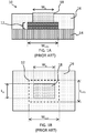
- FIGS 1A and 1B illustrate a known LED-based light source 10 employing this concept, wherein light generated by an LED 12 (on a die substrate 14) is recycled/reflected in a mix box 16 having high reflectivity until it escapes via a small aperture 18.
- the aperture 18 being "small” it is simply meant as being smaller than the LED 12 such that the aperture area A A (i.e. width W A X L A ) is less than the LED area A LED (i.e. width W LED X L LED ) of the LED 12.
- EP 2 216 834 A1 discloses a light-emitting device and its manufacturing method.
- the light-emitting device comprises a first and a second semiconductor diode, a light output section at least partially overlapping both semiconductor diode structures, a layer of optical enhancement material and a light reflection structure enclosing the side surfaces of the first and semiconductor diode structures and the side surfaces of the layer of optical enhancement material.
- a light source comprising: first and second semiconductor diode structures adapted to generate light, the first and second semiconductor diode structures being laterally adjacent to each other; a light output section at least partially overlapping both of the first and second semiconductor diode structures and adapted to output light from the first and second semiconductor diode structures; and a light reflecting structure at least partially enclosing side surfaces of the first and second semiconductor diode structures and the light output section and adapted to reflect light from the semiconductor diode structures towards the light output section, wherein the area of the light output section is less than the combined area of the first and second semiconductor diode structures.
- Embodiments may achieve savings in materials and/or space by arranging light emitting semiconductor diode structures (such as LEDs) to be laterally adjacent and then sharing a single light output section between the adjacent diode structures.
- light emitting semiconductor diode structures such as LEDs
- the light output section can comprise a single component/structure (such as an aperture or an phosphorescent platelet, for example) that is shared across multiple light sources to provide savings/reductions in materials, size, device complexity, and/or manufacturing complexity.
- embodiments may provide a high-luminance light source comprising laterally arranged sub-sources that are overlapped by a common light output section.
- the position(s) and/or shape of the light output section can be changed or designed to enable tiling of the sub-sources such that edges of multiple light output sections can be closely aligned (when viewed from above, for example).
- LED light sources may therefore be strategically arranged in the horizontal axis so that they are overlapped by a single or common light output section.
- pairs of closely positioned LED light sources may be aligned with each other to form a column-like array of pairs such that, when viewed from directly above (i.e. plan view), a single elongate light output section can at least partially overlap each pair of LED light sources in the array.
- the LED light sources of the present disclosure may be any type of LED, such as a Flip Chip type (Thin Film Flip Chip), Patterned Sapphire Substrate, top connected/top emission, top-bottom connected. Also, the light source could be used as naked die, or packaged.
- a Flip Chip type Thin Film Flip Chip
- Patterned Sapphire Substrate Patterned Sapphire Substrate
- top connected/top emission top-bottom connected.
- the light source could be used as naked die, or packaged.
- a light output section (or light emission area) of an LED light source refers to an area towards or through which light from the LED is output (or emitted).
- a cavity or cavities of a LED light source may thus extend towards the light output section.
- the light output section may for example be an area (volume) of the growing template (growth substrate), such as a sapphire.
- Light from the semiconductor structures may be emitted in various directions, thus resulting in some emitted light being incident on the light reflecting structure and reflected back towards the semiconductor structure(s). Light generated by the semiconductor structures may therefore be reflected by the light reflecting structure until it is directed through (and out of) the light output section.
- the arrangement of the light reflecting structure and the light output section may therefore be considered as forming a 'mix-box' structure which reflects light rays until they are output through the light output section.
- the light output direction (from the light output section) may be generalized to be in a vertical direction (e.g. upwardly in the Figures) along which light is output from the light output section.
- the light output direction should be understood to refer to the general upwardly extending direction that light may be output from a light output section, extending away from the surface of the light output section for example.
- the semiconductor diode structures may be arranged such that there is substantially zero separation between adjacent edges of the semiconductor diode structures. In practice, however, it may be difficult to perfectly align adjacent edges to have zero lateral separation. Thus, in embodiments, the semiconductor diode structures are laterally separated by a negligible or small amount. There is a lateral separation between the adjacent edges of the two semiconductor diode structures, and this lateral separation or overlap is less than 10% of the lateral width of the semiconductor diode structures. In embodiments, it may be preferable to reduce such separation to a minimum value (e.g. less than 5% of the lateral width of the semiconductor diode structures, and even more preferably less than 1% of the lateral width of the semiconductor diode structures). In an embodiment, the light output section may comprise an aperture formed in the light reflecting structure.
- the embodiments of the invention further comprise a layer of optical enhancement material below the light output section and at least partially overlapping both of the first and second semiconductor diode structures, wherein the light reflecting structure at least partially encloses side surfaces of the layer of optical enhancement material.
- an embodiment may further comprise a layer of optical enhancement material sandwiched between the top of the semiconductor light sources and the bottom of the light output section.
- the light output section may comprise an optical enhancement material.
- Optical enhancement material may be a 'color conversion fill', such as a phosphorescent material.
- a phosphorescent material examples may include a ceramic phosphor, a phosphor platelet, or a known phosphorescent material referred to as a "lumiramic" material. This may further help to maintain the etendue of the lateral emission area and/or change the color of the emitted light.
- an embodiment comprises a plurality of light output sections
- some or all of the light output sections may comprise (e.g. be filled) with different materials.
- certain light output sections may be filled with a first type of phosphor (e.g. converting blue to white) and others may be filled with another type of phosphor (e.g. converting blue to red).
- Embodiments may be employed in the field of automotive lighting and other fields/applications where high-luminance lighting is desirable.
- an automotive light comprising a light source according to an embodiment.
- a projector light comprising a light source according to an embodiment.
- a method of manufacturing a light source comprising: arranging first and second semiconductor diode structures adapted to generate light to be laterally adjacent to each other; providing a light output section at least partially overlapping both of the first and second semiconductor diode structures, the light output section being adapted to output light from the first and second semiconductor diode structures; and at least partially enclosing sides surfaces of the first and second semiconductor diode structures and the light output section with a light reflecting structure, the light reflecting structure being adapted to reflect light from the semiconductor diode structures towards the light output section, wherein the area of the light output section is less than the combined area of the first and second semiconductor diode structures.
- the step of arranging may comprise arranging the first and second semiconductor diode structures such that there is a lateral separation between the adjacent edges of the first and second semiconductor diode structures, the lateral separation being less than 10% of the lateral width of the first and second semiconductor diode structures.
- the light output section may comprise an aperture formed in the light reflecting structure.
- Embodiments may further comprise forming a layer of optical enhancement material below the light output section and at least partially overlapping both of the first and second semiconductor diode structures, wherein the step of at least partially enclosing sides surfaces of the first and second semiconductor diode structures and the light output section with a light reflecting structure light reflecting structure further comprise at least partially enclosing side surfaces of the layer of optical enhancement material with the light reflecting structure light reflecting structure.
- the light output section may comprise an optical enhancement material.
- the invention provides a light source comprising a plurality of LED light sources and a method for manufacturing the same.
- Embodiments may be of particular relevance to applications that require light of high or increased luminance from a relatively small and/or efficient light source.
- Embodiments employ the concept of arranging light emitting semiconductor diode structures (such as LEDs) to be laterally adjacent and then providing a single light output section (of reduced size compared to the aligned diode structures) overlapping the adjacent diode structures. In this way, a common light output section may be employed or shared across multiple LED light sources to provide savings or reductions in materials and/or manufacturing complexity.
- light emitting semiconductor diode structures such as LEDs
- vertical means substantially orthogonal to the surface of a substrate.
- lateral or horizontal means substantially parallel to the surface of a substrate.
- terms describing positioning or locations are to be construed in conjunction with the orientation of the structures illustrated in the diagrams.
- first layer drawn as being thicker than a second layer may, in practice, be thinner than the second layer.
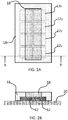
- Figure 2 there is depicted a light source according to an example not forming part of the invention. More specifically, Figure 2A is a plan view of the light source, and Figure 2B is a cross-sectional view of the light source (taken along the line X-X of Figure 2A ).
- the light source comprises a plurality of LEDs 12 positioned on the upper surface of a substrate 20.
- the plurality of LEDs 12 are arranged in a 2x4 array comprising two columns of LEDs 12, each column having four rows of LEDs 12.
- the depicted arrangement of LEDs 12 may be described as comprising four pairs 12 1 , 12 2 , 12 3 , 12 4 of closely-positioned LED light sources 12 which are aligned in a column to form a column-like array of pairs.
- the LEDs 12 can be described as being laterally adjacent to each other since they all lie in the same horizontal plane.
- a light output section 18 is provided on top of the LEDs 12 such that it partially overlaps the top/upper surface of each LED 12.
- the light output section 18 is adapted to output light from the LEDs 12.
- the light output section 18 comprises an optical enhancement material such as phosphorescent material or a lumiramic.
- a single elongate light output section 18 partially overlaps each pair of LEDs 12 in the 2x4 array.
- a single, common light output section 18 partially overlaps all of the LEDs.
- a light reflecting structure 16 encloses the side surfaces of the LEDs 12 and the light output section 18, and also encloses the LED top/upper surfaces that are not covered by the light output section 18.
- the light reflecting structure 16 covers the LEDs 12 and light output section 18 such that only the top/upper surface of the light output section 18 is exposed (i.e. is not covered by the light reflecting structure 16).
- the light reflecting structure 16 comprises a highly reflective material that reflects light from LEDs 12 towards the light output section 18. The light reflecting structure 16 may therefore be considered as forming a light mix box from which light can only escape via the light output section 18.
- the embodiment employs the concept of having a light output section 18 which is smaller than the LEDs 12 it is adapted to output light from. This enables increased luminance from the LEDs 12 to be obtained. Furthermore, the use of a single light output section 18 partially overlapping multiple light generating structures (e.g. LEDs 12) enables a single component or structure to be employed and shared across multiple light sources. A reduction in device complexity and required materials can therefore be obtained.
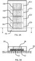
- Figure 3 there is depicted a light source according to another example not forming part of the invention. More specifically, Figure 3A is a plan view of the light source, and Figure 3B is a cross-sectional view of the light source (taken along the line X-X of Figure 3A ).
- each light output section 18 is arranged to partially overlap a respective pair of LEDs.
- a first light output section 18 1 partially overlaps a first pair 12 1 of LEDs
- a second light output section 18 2 partially overlaps a second pair 12 2 of LEDs
- a third light output section 18 3 partially overlaps a third pair 12 3 of LEDs
- a fourth light output section 18 4 partially overlaps a fourth pair 12 4 of LEDs. It will therefore be appreciated that each light output section 18 is arranged to partially overlap two LEDs.
- the area of a light output section 18 is less than the total area of the LEDs it partially covers, thus employing the concept of having a light output section 18 which is smaller than the LEDs 12 it is adapted to output light from.
- This enables increased luminance from the LEDs 12 to be obtained.
- the use of a single light output section 18 partially overlapping two light generating structures e.g. LEDs 12
- Figure 4 there is depicted a light source according to an embodiment of the invention. More specifically, Figure 4A is a plan view of the light source, and Figure 4B is a cross-sectional view of the light source (taken along the line X-X of Figure 4A ).
- the embodiment of Figure 4 is similar to the example of Figure 2 . Detailed description of all of the same or similar technical features will be omitted so as to avoid unnecessary repetition. Instead, it is noted that the embodiment of Figure 4 differs from that of Figure 2 in that the single light output section 18 now comprises an aperture 18 (formed in the light reflecting structure 16). As with the example of Figure 2 , the light output section 18 (i.e. aperture18) of the embodiment of Figure 4 is situated above the LEDs 12 such that it partially overlaps each LED 12. Further, the shape and size of the light output section 18 of Figure 4 is very similar to that of Figure 2 . Thus, the area of the light output section 18 is less than the total area of the LEDs it overlaps, thereby employing the concept of having a light output section 18 which is smaller than the LEDs 12 it is adapted to output light from.
- the light output optical enhancement material comprises a lumiramic or phosphorescent material which is adapted to convert the color of light emitted by the LEDs.
- the light reflecting structure 16 covers the side surfaces of the layer 22 of optical enhancement material as well as a portion of the upper surface of the layer 22 of optical enhancement material. In other words, the light reflecting structure 16 covers the LEDs 12 and layer 22 of optical enhancement material such that only the top/upper surface of layer 22 of optical enhancement material is exposed (i.e. uncovered) by the light output section 18.
- the Figure 4 illustrates an embodiment wherein the light output section 18 comprises an aperture or cavity.
- the layer 22 of optical enhancement material is provided in this embodiment to alter the color of light emitted by the LEDs 12.
- the embodiment of Figure 4 may be modified by replacing the aperture 18 of Figure 4 with optical enhancement material (such as lumiramic or phosphorescent material, for example).
- optical enhancement material such as lumiramic or phosphorescent material, for example.
- the light output section comprises first 24A and second 24B portions of phosphorescent material.
- the first 24A and second 24B portions of phosphorescent material may provide for the alteration of output light to different colors, for example.
- the light reflecting structure 16 may not be entirely reflecting.
- the light reflecting structure may not have substantially 100% reflectivity, and so some light may leak through it. This increases the size of the light outputting area and hence reduces luminance. This may introduce color over position effects (e.g. a blue halo around white light in the center).
- embodiments may be made "light leak tight" by blocking the light with an opaque/reflective coating.
- a reflective coating 30 is provided on the upper surface of the light reflecting structure 16. This helps to lower the overall light transmittance of the light reflecting structure 16 by reflecting light that is incident on the lower surface of the reflective coating 30 from below (e.g. light leaking through the light reflecting structure 16).
Landscapes
- Engineering & Computer Science (AREA)
- Manufacturing & Machinery (AREA)
- Physics & Mathematics (AREA)
- Microelectronics & Electronic Packaging (AREA)
- Optics & Photonics (AREA)
- General Engineering & Computer Science (AREA)
- Led Device Packages (AREA)
Claims (12)
- Lichtquelle, umfassend:erste und zweite Halbleiterdiodenstrukturen (12), die zum Erzeugen von Licht ausgelegt sind, wobei die ersten und zweiten Halbleiterdiodenstruktur lateral benachbart zueinander sind;einen Lichtausgabeabschnitt (18), der sowohl die ersten als auch zweiten Halbleiterdiodenstrukturen wenigstens teilweise überlappt und zum Ausgeben von Licht von den ersten und zweiten Halbleiterdiodenstrukturen ausgelegt ist;eine Schicht aus optischem Verbesserungsmaterial (22) unter dem Lichtausgabeabschnitt, die sowohl die ersten als auch zweiten Halbleiterdiodenstrukturen wenigstens teilweise überlappt; undeine Licht reflektierende Struktur (16), die Seitenflächen der ersten und zweiten Halbleiterdiodenstrukturen und Seitenflächen sowie einen Teil der Oberseite der Schicht aus optischem Verbesserungsmaterial wenigstens teilweise umschließt und zum Reflektieren von Licht von den Halbleiterdiodenstrukturen in Richtung des Lichtausgabeabschnitts ausgelegt ist,wobei die Licht reflektierende Struktur den Lichtausgabeabschnitt umschließt,wobei der Bereich des Lichtausgabeabschnitts kleiner als der kombinierte Bereich der ersten und zweiten Halbleiterdiodenstrukturen und kleiner als der Bereich der Schicht aus optischem Verbesserungsmaterial ist;und wobei eine laterale Trennung zwischen den benachbarten Kanten der ersten und zweiten Halbleiterdiodenstrukturen vorhanden ist, wobei die laterale Trennung weniger als 10 % der lateralen Breite der ersten und zweiten Halbleiterdiodenstrukturen beträgt.
- Lichtquelle nach Anspruch 1, wobei der Lichtausgabeabschnitt eine Öffnung umfasst, die in der Licht reflektierenden Struktur ausgebildet ist.
- Lichtquelle nach Anspruch 1, wobei das optische Verbesserungsmaterial den kombinierten Bereich der ersten und zweiten Halbleiterdiodenstrukturen bedeckt.
- Lichtquelle nach Anspruch 2, wobei die Öffnung der Licht reflektierenden Struktur kein optisches Verbesserungsmaterial umfasst.
- Lichtquelle nach einem der vorhergehenden Ansprüche, wobei mindestens eine der ersten und zweiten Halbleiterdiodenstrukturen eine vorstrukturierte Saphir-LED umfasst.
- Lichtquelle nach einem der vorhergehenden Ansprüche, ferner umfassend eine reflektierende Beschichtung, welche die Licht reflektierende Schicht wenigstens teilweise überlappt.
- Kraftfahrzeugleuchte, umfassend eine Lichtquelle nach einem der vorhergehenden Ansprüche.
- Projektorleuchte, umfassend eine Lichtquelle nach einem der Ansprüche 1 bis 6.
- Verfahren zur Herstellung einer Lichtquelle, umfassend:derartiges Anordnen erster und zweiter Halbleiterdiodenstrukturen (12), die zum Erzeugen von Licht ausgelegt sind, dass sie lateral benachbart zueinander sind;Bereitstellen eines Lichtausgabeabschnitts (18), der sowohl die ersten als auch zweiten Halbleiterdiodenstrukturen wenigstens teilweise überlappt, wobei der Lichtausgabeabschnitt zum Ausgeben von Licht von den ersten und zweiten Halbleiterdiodenstrukturen ausgelegt ist;Bilden einer Schicht aus optischem Verbesserungsmaterial (22) unter dem Lichtausgabeabschnitt, die sowohl die ersten als auch zweiten Halbleiterdiodenstruktur wenigstens teilweise überlappt; undwenigstens teilweises Umschließen von Seitenflächen der ersten und zweiten Halbleiterdiodenstrukturen und der Seitenflächen sowie eines Teils der Oberseite der Schicht aus optischem Verbesserungsmaterial mit einer Licht reflektierenden Struktur (16), wobei die Licht reflektierende Struktur zum Reflektieren von Licht von den Halbleiterdiodenstrukturen in Richtung des Lichtausgabeabschnitts ausgelegt ist,wobei die Licht reflektierende Struktur den Lichtausgabeabschnitt umschließt,wobei der Bereich des Lichtausgabeabschnitts kleiner als der kombinierte Bereich der ersten und zweiten Halbleiterdiodenstrukturen und kleiner als der Bereich der Schicht aus optischem Verbesserungsmaterial ist;und wobei der Schritt des Anordnens ein derartiges Anordnen der ersten und zweiten Halbleiterdiodenstrukturen umfasst, dass eine laterale Trennung zwischen den benachbarten Kanten der ersten und zweiten Halbleiterdiodenstrukturen vorhanden ist, wobei die laterale Trennung weniger als 10 % der lateralen Breite der ersten und zweiten Halbleiterdiodenstrukturen beträgt.
- Verfahren nach Anspruch 9, wobei der Lichtausgabeabschnitt eine Öffnung aufweist, die in der Licht reflektierenden Struktur ausgebildet ist.
- Verfahren nach Anspruch 9, wobei das Bilden einer Schicht aus optischem Verbesserungsmaterial ein Bedecken des kombinierten Bereichs der ersten und zweiten Halbleiterdiodenstrukturen umfasst.
- Verfahren nach Anspruch 10, wobei die Öffnung der Licht reflektierenden Struktur kein optisches Verbesserungsmaterial umfasst.
Applications Claiming Priority (2)
| Application Number | Priority Date | Filing Date | Title |
|---|---|---|---|
| EP14177590 | 2014-07-18 | ||
| PCT/EP2015/066503 WO2016009088A1 (en) | 2014-07-18 | 2015-07-18 | Light emitting diodes and reflector |
Publications (2)
| Publication Number | Publication Date |
|---|---|
| EP3170203A1 EP3170203A1 (de) | 2017-05-24 |
| EP3170203B1 true EP3170203B1 (de) | 2020-05-06 |
Family
ID=51205312
Family Applications (1)
| Application Number | Title | Priority Date | Filing Date |
|---|---|---|---|
| EP15738688.9A Active EP3170203B1 (de) | 2014-07-18 | 2015-07-18 | Leuchtdioden und reflektor |
Country Status (4)
| Country | Link |
|---|---|
| US (1) | US10211187B2 (de) |
| EP (1) | EP3170203B1 (de) |
| CN (1) | CN106663679A (de) |
| WO (1) | WO2016009088A1 (de) |
Families Citing this family (10)
| Publication number | Priority date | Publication date | Assignee | Title |
|---|---|---|---|---|
| CN109791968A (zh) | 2016-07-26 | 2019-05-21 | 克利公司 | 发光二极管、组件和相关方法 |
| TWI626771B (zh) * | 2016-07-26 | 2018-06-11 | 宏齊科技股份有限公司 | 發光二極體單元和薄型平面光源模組 |
| WO2018108734A1 (en) * | 2016-12-15 | 2018-06-21 | Lumileds Holding B.V. | Led module with high near field contrast ratio |
| US11043619B2 (en) | 2016-12-15 | 2021-06-22 | Lumileds Llc | LED module with high near field contrast ratio |
| US11024785B2 (en) | 2018-05-25 | 2021-06-01 | Creeled, Inc. | Light-emitting diode packages |
| US11335833B2 (en) | 2018-08-31 | 2022-05-17 | Creeled, Inc. | Light-emitting diodes, light-emitting diode arrays and related devices |
| US11233183B2 (en) | 2018-08-31 | 2022-01-25 | Creeled, Inc. | Light-emitting diodes, light-emitting diode arrays and related devices |
| USD902448S1 (en) | 2018-08-31 | 2020-11-17 | Cree, Inc. | Light emitting diode package |
| US11101411B2 (en) | 2019-06-26 | 2021-08-24 | Creeled, Inc. | Solid-state light emitting devices including light emitting diodes in package structures |
| DE102023106274A1 (de) * | 2023-03-14 | 2024-09-19 | Ams-Osram International Gmbh | Leuchtvorrichtung und verfahren zum herstellen einer leuchtvorrichtung |
Family Cites Families (11)
| Publication number | Priority date | Publication date | Assignee | Title |
|---|---|---|---|---|
| WO2006016324A1 (en) | 2004-08-06 | 2006-02-16 | Koninklijke Philips Electronics N. V. | Light engine |
| EP2573812B1 (de) | 2006-10-12 | 2017-08-16 | Panasonic Intellectual Property Management Co., Ltd. | Lichtemittierende Vorrichtung |
| DE102007011123A1 (de) * | 2007-03-07 | 2008-09-11 | Osram Opto Semiconductors Gmbh | Licht emittierendes Modul und Herstellungsverfahren für ein Licht emittierendes Modul |
| US7700967B2 (en) * | 2007-05-25 | 2010-04-20 | Philips Lumileds Lighting Company Llc | Illumination device with a wavelength converting element held by a support structure having an aperture |
| KR101517644B1 (ko) * | 2007-11-29 | 2015-05-04 | 니치아 카가쿠 고교 가부시키가이샤 | 발광장치 및 그 제조방법 |
| KR20100127286A (ko) * | 2008-03-21 | 2010-12-03 | 코닌클리즈케 필립스 일렉트로닉스 엔.브이. | 발광 장치 |
| CN102187485B (zh) * | 2008-10-15 | 2013-07-03 | 株式会社小糸制作所 | 发光模块、发光模块的制造方法及灯具单元 |
| DE102012214219A1 (de) | 2012-08-09 | 2014-02-13 | Osram Gmbh | LED-Modul |
| US9337405B2 (en) * | 2012-08-31 | 2016-05-10 | Nichia Corporation | Light emitting device and method for manufacturing the same |
| US9188288B2 (en) * | 2012-09-28 | 2015-11-17 | Tsmc Solid State Lighting Ltd. | LED emitter with improved white color appearance |
| DE102012110774A1 (de) | 2012-11-09 | 2014-05-15 | Osram Opto Semiconductors Gmbh | Optoelektronisches Halbleiterbauteil |
-
2015
- 2015-07-18 EP EP15738688.9A patent/EP3170203B1/de active Active
- 2015-07-18 CN CN201580038991.5A patent/CN106663679A/zh active Pending
- 2015-07-18 US US15/326,484 patent/US10211187B2/en active Active
- 2015-07-18 WO PCT/EP2015/066503 patent/WO2016009088A1/en not_active Ceased
Non-Patent Citations (1)
| Title |
|---|
| None * |
Also Published As
| Publication number | Publication date |
|---|---|
| US20170207202A1 (en) | 2017-07-20 |
| US10211187B2 (en) | 2019-02-19 |
| WO2016009088A1 (en) | 2016-01-21 |
| EP3170203A1 (de) | 2017-05-24 |
| CN106663679A (zh) | 2017-05-10 |
Similar Documents
| Publication | Publication Date | Title |
|---|---|---|
| US10211187B2 (en) | Light emitting diodes and reflector | |
| JP2012502488A (ja) | 多層led蛍光体 | |
| KR102507965B1 (ko) | 광원 | |
| US10825971B2 (en) | Light-emitting device including a Distributed Bragg Reflector (DBR) film | |
| EP3170202B1 (de) | Leuchtdiodenlichtquelle für automobilanwendung | |
| JP6757716B2 (ja) | 光源、その製造方法、及びライト | |
| JP2010092765A (ja) | 照明装置 | |
| CN114335060B (zh) | 防串扰微显示阵列 | |
| US10541267B2 (en) | Light-emitting assembly and method for producing a light-emitting assembly | |
| JP2021163807A (ja) | 発光装置 | |
| JP7299522B2 (ja) | 発光モジュール及び面状光源 | |
| JP2015153815A (ja) | 発光モジュールおよび照明装置 | |
| JP7518373B2 (ja) | 発光装置 | |
| TWM565405U (zh) | LED lighting device | |
| TWI475725B (zh) | 使用預製螢光帽蓋以調整空間色彩均勻度與配光曲線的發光二極體封裝結構 | |
| TW201023389A (en) | Multi-colors package with single chip | |
| TW201822381A (zh) | 發光二極體封裝結構 | |
| KR20130101742A (ko) | 엘이디 패키지 |
Legal Events
| Date | Code | Title | Description |
|---|---|---|---|
| STAA | Information on the status of an ep patent application or granted ep patent |
Free format text: STATUS: THE INTERNATIONAL PUBLICATION HAS BEEN MADE |
|
| PUAI | Public reference made under article 153(3) epc to a published international application that has entered the european phase |
Free format text: ORIGINAL CODE: 0009012 |
|
| STAA | Information on the status of an ep patent application or granted ep patent |
Free format text: STATUS: REQUEST FOR EXAMINATION WAS MADE |
|
| 17P | Request for examination filed |
Effective date: 20170220 |
|
| AK | Designated contracting states |
Kind code of ref document: A1 Designated state(s): AL AT BE BG CH CY CZ DE DK EE ES FI FR GB GR HR HU IE IS IT LI LT LU LV MC MK MT NL NO PL PT RO RS SE SI SK SM TR |
|
| AX | Request for extension of the european patent |
Extension state: BA ME |
|
| DAV | Request for validation of the european patent (deleted) | ||
| DAX | Request for extension of the european patent (deleted) | ||
| RAP1 | Party data changed (applicant data changed or rights of an application transferred) |
Owner name: LUMILEDS HOLDING B.V. |
|
| RAP1 | Party data changed (applicant data changed or rights of an application transferred) |
Owner name: LUMILEDS HOLDING B.V. |
|
| GRAP | Despatch of communication of intention to grant a patent |
Free format text: ORIGINAL CODE: EPIDOSNIGR1 |
|
| STAA | Information on the status of an ep patent application or granted ep patent |
Free format text: STATUS: GRANT OF PATENT IS INTENDED |
|
| INTG | Intention to grant announced |
Effective date: 20200123 |
|
| GRAS | Grant fee paid |
Free format text: ORIGINAL CODE: EPIDOSNIGR3 |
|
| GRAA | (expected) grant |
Free format text: ORIGINAL CODE: 0009210 |
|
| STAA | Information on the status of an ep patent application or granted ep patent |
Free format text: STATUS: THE PATENT HAS BEEN GRANTED |
|
| AK | Designated contracting states |
Kind code of ref document: B1 Designated state(s): AL AT BE BG CH CY CZ DE DK EE ES FI FR GB GR HR HU IE IS IT LI LT LU LV MC MK MT NL NO PL PT RO RS SE SI SK SM TR |
|
| REG | Reference to a national code |
Ref country code: GB Ref legal event code: FG4D |
|
| REG | Reference to a national code |
Ref country code: CH Ref legal event code: EP Ref country code: AT Ref legal event code: REF Ref document number: 1268189 Country of ref document: AT Kind code of ref document: T Effective date: 20200515 |
|
| REG | Reference to a national code |
Ref country code: IE Ref legal event code: FG4D |
|
| REG | Reference to a national code |
Ref country code: DE Ref legal event code: R096 Ref document number: 602015052199 Country of ref document: DE |
|
| REG | Reference to a national code |
Ref country code: LT Ref legal event code: MG4D |
|
| REG | Reference to a national code |
Ref country code: NL Ref legal event code: MP Effective date: 20200506 |
|
| PG25 | Lapsed in a contracting state [announced via postgrant information from national office to epo] |
Ref country code: SE Free format text: LAPSE BECAUSE OF FAILURE TO SUBMIT A TRANSLATION OF THE DESCRIPTION OR TO PAY THE FEE WITHIN THE PRESCRIBED TIME-LIMIT Effective date: 20200506 Ref country code: IS Free format text: LAPSE BECAUSE OF FAILURE TO SUBMIT A TRANSLATION OF THE DESCRIPTION OR TO PAY THE FEE WITHIN THE PRESCRIBED TIME-LIMIT Effective date: 20200906 Ref country code: NO Free format text: LAPSE BECAUSE OF FAILURE TO SUBMIT A TRANSLATION OF THE DESCRIPTION OR TO PAY THE FEE WITHIN THE PRESCRIBED TIME-LIMIT Effective date: 20200806 Ref country code: FI Free format text: LAPSE BECAUSE OF FAILURE TO SUBMIT A TRANSLATION OF THE DESCRIPTION OR TO PAY THE FEE WITHIN THE PRESCRIBED TIME-LIMIT Effective date: 20200506 Ref country code: GR Free format text: LAPSE BECAUSE OF FAILURE TO SUBMIT A TRANSLATION OF THE DESCRIPTION OR TO PAY THE FEE WITHIN THE PRESCRIBED TIME-LIMIT Effective date: 20200807 Ref country code: PT Free format text: LAPSE BECAUSE OF FAILURE TO SUBMIT A TRANSLATION OF THE DESCRIPTION OR TO PAY THE FEE WITHIN THE PRESCRIBED TIME-LIMIT Effective date: 20200907 Ref country code: LT Free format text: LAPSE BECAUSE OF FAILURE TO SUBMIT A TRANSLATION OF THE DESCRIPTION OR TO PAY THE FEE WITHIN THE PRESCRIBED TIME-LIMIT Effective date: 20200506 |
|
| PG25 | Lapsed in a contracting state [announced via postgrant information from national office to epo] |
Ref country code: HR Free format text: LAPSE BECAUSE OF FAILURE TO SUBMIT A TRANSLATION OF THE DESCRIPTION OR TO PAY THE FEE WITHIN THE PRESCRIBED TIME-LIMIT Effective date: 20200506 Ref country code: LV Free format text: LAPSE BECAUSE OF FAILURE TO SUBMIT A TRANSLATION OF THE DESCRIPTION OR TO PAY THE FEE WITHIN THE PRESCRIBED TIME-LIMIT Effective date: 20200506 Ref country code: RS Free format text: LAPSE BECAUSE OF FAILURE TO SUBMIT A TRANSLATION OF THE DESCRIPTION OR TO PAY THE FEE WITHIN THE PRESCRIBED TIME-LIMIT Effective date: 20200506 Ref country code: BG Free format text: LAPSE BECAUSE OF FAILURE TO SUBMIT A TRANSLATION OF THE DESCRIPTION OR TO PAY THE FEE WITHIN THE PRESCRIBED TIME-LIMIT Effective date: 20200806 |
|
| REG | Reference to a national code |
Ref country code: AT Ref legal event code: MK05 Ref document number: 1268189 Country of ref document: AT Kind code of ref document: T Effective date: 20200506 |
|
| PG25 | Lapsed in a contracting state [announced via postgrant information from national office to epo] |
Ref country code: NL Free format text: LAPSE BECAUSE OF FAILURE TO SUBMIT A TRANSLATION OF THE DESCRIPTION OR TO PAY THE FEE WITHIN THE PRESCRIBED TIME-LIMIT Effective date: 20200506 Ref country code: AL Free format text: LAPSE BECAUSE OF FAILURE TO SUBMIT A TRANSLATION OF THE DESCRIPTION OR TO PAY THE FEE WITHIN THE PRESCRIBED TIME-LIMIT Effective date: 20200506 |
|
| PG25 | Lapsed in a contracting state [announced via postgrant information from national office to epo] |
Ref country code: SM Free format text: LAPSE BECAUSE OF FAILURE TO SUBMIT A TRANSLATION OF THE DESCRIPTION OR TO PAY THE FEE WITHIN THE PRESCRIBED TIME-LIMIT Effective date: 20200506 Ref country code: IT Free format text: LAPSE BECAUSE OF FAILURE TO SUBMIT A TRANSLATION OF THE DESCRIPTION OR TO PAY THE FEE WITHIN THE PRESCRIBED TIME-LIMIT Effective date: 20200506 Ref country code: EE Free format text: LAPSE BECAUSE OF FAILURE TO SUBMIT A TRANSLATION OF THE DESCRIPTION OR TO PAY THE FEE WITHIN THE PRESCRIBED TIME-LIMIT Effective date: 20200506 Ref country code: DK Free format text: LAPSE BECAUSE OF FAILURE TO SUBMIT A TRANSLATION OF THE DESCRIPTION OR TO PAY THE FEE WITHIN THE PRESCRIBED TIME-LIMIT Effective date: 20200506 Ref country code: ES Free format text: LAPSE BECAUSE OF FAILURE TO SUBMIT A TRANSLATION OF THE DESCRIPTION OR TO PAY THE FEE WITHIN THE PRESCRIBED TIME-LIMIT Effective date: 20200506 Ref country code: AT Free format text: LAPSE BECAUSE OF FAILURE TO SUBMIT A TRANSLATION OF THE DESCRIPTION OR TO PAY THE FEE WITHIN THE PRESCRIBED TIME-LIMIT Effective date: 20200506 Ref country code: CZ Free format text: LAPSE BECAUSE OF FAILURE TO SUBMIT A TRANSLATION OF THE DESCRIPTION OR TO PAY THE FEE WITHIN THE PRESCRIBED TIME-LIMIT Effective date: 20200506 Ref country code: RO Free format text: LAPSE BECAUSE OF FAILURE TO SUBMIT A TRANSLATION OF THE DESCRIPTION OR TO PAY THE FEE WITHIN THE PRESCRIBED TIME-LIMIT Effective date: 20200506 |
|
| REG | Reference to a national code |
Ref country code: DE Ref legal event code: R097 Ref document number: 602015052199 Country of ref document: DE |
|
| PG25 | Lapsed in a contracting state [announced via postgrant information from national office to epo] |
Ref country code: SK Free format text: LAPSE BECAUSE OF FAILURE TO SUBMIT A TRANSLATION OF THE DESCRIPTION OR TO PAY THE FEE WITHIN THE PRESCRIBED TIME-LIMIT Effective date: 20200506 Ref country code: PL Free format text: LAPSE BECAUSE OF FAILURE TO SUBMIT A TRANSLATION OF THE DESCRIPTION OR TO PAY THE FEE WITHIN THE PRESCRIBED TIME-LIMIT Effective date: 20200506 Ref country code: MC Free format text: LAPSE BECAUSE OF FAILURE TO SUBMIT A TRANSLATION OF THE DESCRIPTION OR TO PAY THE FEE WITHIN THE PRESCRIBED TIME-LIMIT Effective date: 20200506 |
|
| REG | Reference to a national code |
Ref country code: CH Ref legal event code: PL |
|
| PLBE | No opposition filed within time limit |
Free format text: ORIGINAL CODE: 0009261 |
|
| STAA | Information on the status of an ep patent application or granted ep patent |
Free format text: STATUS: NO OPPOSITION FILED WITHIN TIME LIMIT |
|
| 26N | No opposition filed |
Effective date: 20210209 |
|
| REG | Reference to a national code |
Ref country code: BE Ref legal event code: MM Effective date: 20200731 |
|
| PG25 | Lapsed in a contracting state [announced via postgrant information from national office to epo] |
Ref country code: CH Free format text: LAPSE BECAUSE OF NON-PAYMENT OF DUE FEES Effective date: 20200731 Ref country code: LU Free format text: LAPSE BECAUSE OF NON-PAYMENT OF DUE FEES Effective date: 20200718 Ref country code: LI Free format text: LAPSE BECAUSE OF NON-PAYMENT OF DUE FEES Effective date: 20200731 |
|
| PG25 | Lapsed in a contracting state [announced via postgrant information from national office to epo] |
Ref country code: BE Free format text: LAPSE BECAUSE OF NON-PAYMENT OF DUE FEES Effective date: 20200731 Ref country code: SI Free format text: LAPSE BECAUSE OF FAILURE TO SUBMIT A TRANSLATION OF THE DESCRIPTION OR TO PAY THE FEE WITHIN THE PRESCRIBED TIME-LIMIT Effective date: 20200506 |
|
| PG25 | Lapsed in a contracting state [announced via postgrant information from national office to epo] |
Ref country code: IE Free format text: LAPSE BECAUSE OF NON-PAYMENT OF DUE FEES Effective date: 20200718 |
|
| PG25 | Lapsed in a contracting state [announced via postgrant information from national office to epo] |
Ref country code: TR Free format text: LAPSE BECAUSE OF FAILURE TO SUBMIT A TRANSLATION OF THE DESCRIPTION OR TO PAY THE FEE WITHIN THE PRESCRIBED TIME-LIMIT Effective date: 20200506 Ref country code: MT Free format text: LAPSE BECAUSE OF FAILURE TO SUBMIT A TRANSLATION OF THE DESCRIPTION OR TO PAY THE FEE WITHIN THE PRESCRIBED TIME-LIMIT Effective date: 20200506 Ref country code: CY Free format text: LAPSE BECAUSE OF FAILURE TO SUBMIT A TRANSLATION OF THE DESCRIPTION OR TO PAY THE FEE WITHIN THE PRESCRIBED TIME-LIMIT Effective date: 20200506 |
|
| PG25 | Lapsed in a contracting state [announced via postgrant information from national office to epo] |
Ref country code: MK Free format text: LAPSE BECAUSE OF FAILURE TO SUBMIT A TRANSLATION OF THE DESCRIPTION OR TO PAY THE FEE WITHIN THE PRESCRIBED TIME-LIMIT Effective date: 20200506 |
|
| P01 | Opt-out of the competence of the unified patent court (upc) registered |
Effective date: 20230530 |
|
| REG | Reference to a national code |
Ref country code: DE Ref legal event code: R079 Ref document number: 602015052199 Country of ref document: DE Free format text: PREVIOUS MAIN CLASS: H01L0025075000 Ipc: H10H0029240000 |
|
| PGFP | Annual fee paid to national office [announced via postgrant information from national office to epo] |
Ref country code: DE Payment date: 20250728 Year of fee payment: 11 |
|
| PGFP | Annual fee paid to national office [announced via postgrant information from national office to epo] |
Ref country code: GB Payment date: 20250722 Year of fee payment: 11 |
|
| PGFP | Annual fee paid to national office [announced via postgrant information from national office to epo] |
Ref country code: FR Payment date: 20250725 Year of fee payment: 11 |