EP3174209A1 - Treiberschaltung zur signalübertragung - Google Patents
Treiberschaltung zur signalübertragung Download PDFInfo
- Publication number
- EP3174209A1 EP3174209A1 EP16169102.7A EP16169102A EP3174209A1 EP 3174209 A1 EP3174209 A1 EP 3174209A1 EP 16169102 A EP16169102 A EP 16169102A EP 3174209 A1 EP3174209 A1 EP 3174209A1
- Authority
- EP
- European Patent Office
- Prior art keywords
- output terminal
- data input
- current
- drive unit
- mode drive
- Prior art date
- Legal status (The legal status is an assumption and is not a legal conclusion. Google has not performed a legal analysis and makes no representation as to the accuracy of the status listed.)
- Withdrawn
Links
- 230000008054 signal transmission Effects 0.000 title description 3
- 238000010168 coupling process Methods 0.000 claims abstract description 10
- 230000008878 coupling Effects 0.000 claims abstract description 8
- 238000005859 coupling reaction Methods 0.000 claims abstract description 8
- 230000003111 delayed effect Effects 0.000 claims description 10
- 230000004044 response Effects 0.000 claims description 7
- 238000010586 diagram Methods 0.000 description 32
- 230000007246 mechanism Effects 0.000 description 10
- 230000001965 increasing effect Effects 0.000 description 6
- 239000003990 capacitor Substances 0.000 description 4
- 230000003247 decreasing effect Effects 0.000 description 3
- 238000012986 modification Methods 0.000 description 3
- 230000004048 modification Effects 0.000 description 3
- 230000008859 change Effects 0.000 description 1
- 230000001419 dependent effect Effects 0.000 description 1
- 238000011161 development Methods 0.000 description 1
- 230000018109 developmental process Effects 0.000 description 1
- 230000002708 enhancing effect Effects 0.000 description 1
- 238000000034 method Methods 0.000 description 1
- 230000003071 parasitic effect Effects 0.000 description 1
Images


Classifications
-
- H—ELECTRICITY
- H03—ELECTRONIC CIRCUITRY
- H03K—PULSE TECHNIQUE
- H03K19/00—Logic circuits, i.e. having at least two inputs acting on one output; Inverting circuits
- H03K19/0175—Coupling arrangements; Interface arrangements
- H03K19/017545—Coupling arrangements; Impedance matching circuits
-
- H—ELECTRICITY
- H03—ELECTRONIC CIRCUITRY
- H03K—PULSE TECHNIQUE
- H03K19/00—Logic circuits, i.e. having at least two inputs acting on one output; Inverting circuits
- H03K19/0175—Coupling arrangements; Interface arrangements
- H03K19/017509—Interface arrangements
- H03K19/017518—Interface arrangements using a combination of bipolar and field effect transistors [BIFET]
- H03K19/017527—Interface arrangements using a combination of bipolar and field effect transistors [BIFET] with at least one differential stage
-
- H—ELECTRICITY
- H03—ELECTRONIC CIRCUITRY
- H03M—CODING; DECODING; CODE CONVERSION IN GENERAL
- H03M9/00—Parallel/series conversion or vice versa
Definitions
- the present invention relates to a driver circuit for signal transmission according to the pre-characterizing clause of claim 1.
- SerDes serializer/deserializer
- driver circuits including a current mode logic (CML) driver, a voltage mode driver, and an H-bridge current mode driver having a resistor coupled between a differential output terminals (referred to hereinafter as an H-bridge driver).
- CML current mode logic
- voltage mode driver consumes more power.
- the voltage mode driver lacks design flexibility and is therefore unsuitable for transmitter (TX) equalizer design. Power efficiency of the H-bridge driver is higher than that of the CML driver but still lower than that of the voltage mode driver.
- the present invention aims at providing a driver circuit capable of referring to data logic to couple reference voltage(s) and reference current(s) to a terminal element and a related control method thereof for reducing the power consumption and enhancing design flexibility.
- the claimed driver circuit for receiving a first data input and generating an output signal to a termination element according to at least the first data input includes a first output terminal, a first current mode drive unit and a first voltage mode drive unit.
- the first output terminal is arranged for outputting the output signal.
- the first current mode drive unit is coupled to the first output terminal, and is arranged for generating a first reference current, selectively outputting the first reference current from the first output terminal to the termination element according to the first data input, and selectively receiving the first reference current through the first output terminal according to the first data input, wherein when the first current mode drive unit outputs the first reference current, the first current mode drive unit steers the first reference current to flow into the termination element such that the first reference current outputted from the first current mode drive unit flows through the termination element and is used as at least a portion of a current flowing through the termination element.
- the first voltage mode drive unit is coupled to the first output terminal, and is arranged for coupling one of a first reference voltage and a second reference voltage to the first output terminal according to the first data input, wherein the first reference voltage is different from the second reference voltage.
- the proposed driver circuit may provide a reference current and a plurality of reference voltages, wherein when the reference current is outputted from one of a pair of differential output terminals according to data logic, the reference voltages may be coupled to different output terminals of the pair of differential output terminals, respectively, thus implementing a driver architecture consuming less power.
- the power consumption of the proposed driver circuit may be even less than that of a voltage mode driver.
- the proposed driver control mechanism may be employed in a single-ended driver circuit. Further, the proposed driver control mechanism may be employed in multi-level driver and a transmit finite impulse response (FIR) equalizer. Moreover, the proposed driver circuit may be employed in equalizer architecture due to high design flexibility.
- FIR transmit finite impulse response
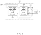
- FIG. 1 is a block diagram illustrating an exemplary driver circuit according to an embodiment of the present invention.
- the driver circuit 100 may be employed in a SerDes transmitter (not shown in FIG. 1 ).
- the driver circuit 100 may receive a data input DIN 0 and generate an output signal S OUT to a termination element (implemented by a termination resistor R T in this embodiment) according to the data input DIN 0 , wherein the termination resistor R T may be located in a SerDes receiver (not shown in FIG. 1 ).
- the driver circuit 100 may include a pair of differential output terminals 102 (having an output terminal T 1 and an output terminal T 2 ), a current mode drive unit 110 and a voltage mode drive unit 120.
- the output signal S OUT may be regarded as a voltage difference between the output terminal T 1 and the output terminal T 2 , and correspond to an output data logic (e.g. a logic "1" corresponding to a positive voltage or a logic "0" corresponding to a negative voltage).
- an output data logic e.g. a logic "1" corresponding to a positive voltage or a logic "0" corresponding to a negative voltage.
- the current mode drive unit 110 is coupled to the pair of differential output terminals 102, and is arranged for generating a reference current I R , wherein the current mode drive unit 110 may output the reference current I R from one of the output terminal T 1 and the output terminal T 2 according to the data input DIN 0 , and receive the reference current I R from the other of the output terminal T 1 and the output terminal T 2 according to the data input DIN 0 .
- the reference current I R may flow through the termination resistor R T first, and then flows into the current mode drive unit 110 through the other of the output terminal T 1 and the output terminal T 2 .
- the current mode drive unit 110 may change a direction of the reference current I R through the termination resistor R T , thereby changing respective electric potentials of the output terminal T 1 and the output terminal T 2 .
- the output signal S OUT may correspond to a specific output data logic (e.g. a logic "1").
- the output signal S OUT may correspond to another specific output data logic (e.g. a logic "0") .
- a voltage difference between the output terminal T 1 and the output terminal T 2 may be a voltage drop across the termination resistor R T due to the reference current I R flowing therethrough, which implies that an output current of the current mode drive unit 110 may be effectively provided for the SerDes receiver.
- the voltage mode drive unit 120 is coupled to the pair of differential output terminals 102, and is arranged for providing a reference voltage V R1 and a reference voltage V R2 different from the reference voltage V R1 , wherein the voltage mode drive unit 120 may couple the reference voltage V R1 to one of the output terminal T 1 and the output terminal T 2 according to the data input DIN 0 , and couple the reference voltage V R2 to the other of the output terminal T 1 and the output terminal T 2 according to the data input DIN 0 .
- the reference voltage V R1 and the reference voltage V R2 may be provided for two output terminals of the pair of differential output terminals 102, respectively, so that the output terminal T 1 and the output terminal T 2 may have different electric potentials to provide an output voltage required by the SerDes receiver.
- the output signal S OUT may correspond to a specific output data logic (e.g. a logic "1"); and when the reference voltage V R1 is coupled to the output terminal T 2 and the reference voltage V R2 is coupled to the output terminal T 1 , the output signal S OUT may correspond to another specific output data logic (e.g. a logic "0").
- a specific output data logic e.g. a logic "1”
- another specific output data logic e.g. a logic "0"
- electric potential of one of the output terminal T 1 and the output terminal T 2 may be equal to the reference voltage V R1
- electric potential of the other of the output terminal T 1 and the output terminal T 2 may be equal to the reference voltage V R2 , which implies that an output voltage of the voltage mode drive unit 120 may be effectively provided for the pair of differential output terminals 102.
- the current mode drive unit 110 may provide the output current effectively, and the voltage mode drive unit 120 may provide the output voltage effectively.
- a power efficient driver circuit can be provided.
- the voltage mode drive unit 120 may couple the reference voltage V R1 to the output terminal T 1 and couple the reference voltage V R2 to the output terminal T 2 according to the data input DIN 0 .
- a drive current outputted from the driver circuit 100 may be provided by the current mode drive unit 110 only, thus greatly reducing power consumption.
- the drive current outputted from the driver circuit 100 may come from the current mode drive unit 110 and the voltage mode drive unit 120.
- the drive current outputted from the driver circuit 100 may be a sum of the reference current I R and an output current of the voltage mode drive unit 120, wherein a ratio of the reference current I R to the drive current outputted from the driver circuit 100 may adjusted according to actual requirements/considerations.
- the reference voltage V R1 and/or the reference voltage V R2 provided by the voltage mode drive unit 120 may be generated within the driver circuit 100 or generated by a circuit external to driver circuit 100.
- the voltage mode drive unit 120 may include a voltage generation circuit (not shown in FIG. 1 ), which is used for generating at least one of the reference voltage V R1 and the reference voltage V R2 .
- at least one of the reference voltage V R1 and the reference voltage V R2 may be directly provided by a voltage generation circuit external coupled to the driver circuit 100, such as a system power supply or a ground terminal.
- the voltage mode drive unit 120 may provide the reference voltage V R1 and the reference voltage V R2 by coupling a voltage, supplied from an external circuit, to output terminal(s) of a differential pair of output terminals.
- FIG. 2 is a diagram illustrating a first implementation of the driver circuit 100 shown in FIG. 1 .
- the driver circuit 200 may include the output terminals T 1 and T 2 shown in FIG. 1 (i.e. a pair of differential output terminals), a current mode drive unit 210 and a voltage mode drive unit 220, wherein the current mode drive unit 110 and the voltage mode drive unit 120 shown in FIG. 1 may be implemented by the current mode drive unit 210 and the voltage mode drive unit 220, respectively.
- a symbol VDD denotes a direct current (DC) power required by circuit elements
- a symbol GND denotes a reference voltage node (e.g. a common ground).
- the current mode drive unit 210 may include a current source IS 0 and a current sink IS 0 '.
- the current source IS 0 may be arranged for generating the reference current I R
- the current sink IS 0 ' may be arranged for receiving the reference current I R
- the current source IS 0 may be coupled to one of the output terminal T 1 and the output terminal T 2 according to the data input DIN 0
- the current sink IS 0 ' may be coupled to the other of the output terminal T 1 and the output terminal T 2 according to the data input DIN 0 .
- the current mode drive unit 210 may include further include a plurality of switches S C1 -S C4 , wherein the switch S C1 may be selectively coupled between the current source IS 0 and the output terminal T 1 according to the data input DIN 0 ; the switch S C2 may be selectively coupled between the current source IS 0 and the output terminal T 2 according to the data input DIN 0 ; the switch S C3 may be selectively coupled between the current sink IS 0 ' and the output terminal T 1 according to the data input DIN 0 ; and the switch S C4 may be selectively coupled between the current sink IS 0 ' and the output terminal T 2 according to the data input DIN 0 .
- the current source IS 0 may output the reference current I R from one of the output terminal T 1 and the output terminal T 2
- the current sink IS 0 ' may draw the reference current I R from the other of the output terminal T 1 and the output terminal T 2 .
- the data input DIN 0 may include a data signal DP 0 and a data signal DN 0 , wherein the data signal DP 0 and the data signal DN 0 may be inverted with respect to each other, or non-overlapping signals.
- the data signal DP 0 may control switch states of the switches S C1 and S C3 , wherein when one of the switches S C1 and S C3 is switched on, the other of the switches S C1 and S C3 is switched off.
- the data signal DN 0 may control switch states of the switches S C2 and S C4 , wherein when one of the switches S C2 and S C4 is switched on, the other of the switches S C2 and S C4 is switched off.
- the switch S C1 when the switch S C1 is switched on due to the data signal DP 0 , the switch S C2 is switched off due to the data signal DN 0 , and when the switch S C1 is switched off due to the data signal DP 0 , the switch S C2 is switched on due to the data signal DN 0 .
- the current source IS 0 may output the reference current I R from one of the output terminal T 1 and the output terminal T 2 according to the data input DIN 0
- current sink IS 0 ' may draw the reference current I R from the other of the output terminal T 1 and the output terminal T 2 according to the data input DIN 0
- the switches S C1 and S C2 (or the switches S C3 and S C4 ) may be replaced by a three-way switch.
- the current mode drive unit 210 may output the reference current I R from one of the output terminal T 1 and the output terminal T 2 and receive the reference current I R from the other of the output terminal T 1 and the output terminal T 2 according to the data input DIN 0 , other variations and modifications fall within the spirit and scope of the present invention.
- the voltage mode drive unit 220 may include a plurality of voltage sources VS A -VS D , a plurality of switches S V1 -S V4 , and a plurality of impedance elements (implemented by resistors R 1 and R 2 in this implementation).
- the voltage sources VS A and VS B may be used to generate the reference voltage V R1 shown in FIG. 1
- the voltage sources VS C and VS D may be used to generate the reference voltage V R2 shown in FIG. 1 .
- the resistor R 1 is coupled between a node N 1 and the output terminal T 1
- the resistor R 2 is coupled between a node N 2 and the output terminal T 2
- the node N 1 may be coupled to the reference voltage V R1 through the switch S V1 or coupled to the reference voltage V R2 through the switch S V3 according to the data input DIN 0
- the node N 2 may be coupled to the reference voltage V R1 through the switch S V2 or coupled to the reference voltage V R2 through the switch S V4 according to the data input DIN 0 .
- the switch S V1 maybe selectively coupled between the reference voltage V R1 (the voltage source VS A ) and the output terminal T 1 (through the resistor R 1 ) according to the data input DIN 0 ;
- the switch S V2 may be selectively coupled between the reference voltage V R1 (the voltage source VS B ) and the output terminal T 2 (through the resistor R 2 ) according to the data input DIN 0 ;
- the switch S V3 may be selectively coupled between the reference voltage V R2 (the voltage source VS C ) and the output terminal T 1 (through the resistor R 1 ) according to the data input DIN 0 ;
- the switch S V4 may be selectively coupled between the reference voltage V R2 (the voltage source VS D ) and the output terminal T 2 (through the resistor R 2 ) according to the data input DIN 0 .
- the switch S V1 and the switch S V4 are switched on due to the data input DIN 0
- the switch S V2 and the switch S V3 are switched off
- the switch S V1 and the switch S V4 are switched off due to the data input DIN 0
- the switch S V2 and the switch S V3 are switched on.
- the data signal DP 0 may control switch states of the switches S V1 and S V3 , wherein when one of the switches S V1 and S V3 is switched on, the other of the switches S V1 and S V3 is switched off.
- the data signal DN 0 may control switch states of the switches S V2 and S V4 , wherein when one of the switches S V2 and S V4 is switched on, the other of the switches S V2 and S V4 is switched off. Further, when the switch S V1 is switched on due to the data signal DP 0 , the switch S V2 is switched off due to the data signal DN 0 , and when the switch S V1 is switched off due to the data signal DP 0 , the switch S V2 is switched on due to the data signal DN 0 .
- FIG. 3 is a diagram illustrating an exemplary output operation of the driver circuit 200 shown in FIG. 2
- FIG. 4 is a diagram illustrating another exemplary output operation of the driver circuit 200 shown in FIG. 2 .
- a voltage difference obtained by subtracting a voltage of the output terminal T 2 from a voltage of the output terminal T 1 is used as the output signal S OUT in the embodiments shown in FIG. 3 and FIG. 4 .
- the output signal S OUT corresponds to a data logic "1"; and when the voltage of the output terminal T 1 is less than the voltage of the output terminal T 2 , the output signal S OUT corresponds to a data logic "0".
- the reference voltage V R1 generated by the voltage sources VS A and VS B is greater than the reference voltage V R2 generated by the voltage sources VS C and VS D .
- the aforementioned definition of the data logic and a magnitude relationship between the reference voltages are for illustrative purposes only, and are not meant to be limitations of the present invention.
- the reference current I R generated from the current source IS 0 may be outputted from the output terminal T 1 to the termination resistor R T through the switch S C1 , and then flow into the current sink IS 0 ' through the output terminal T 2 and the switch S C4 . Additionally, the switches S V1 and S V4 are switched on, allowing the reference voltage V R1 (a high voltage) and the reference voltage V R2 (a low voltage) to be coupled to the output terminal T 1 and the output terminal T 2 respectively.
- the output signal S OUT may correspond to a data logic "1". In the embodiment shown in FIG.
- the reference current I R generated from the current source IS 0 may be outputted from the output terminal T 2 to the termination resistor R T through the switch S C2 , and then flow into the current sink IS 0 ' through the output terminal T 1 and the switch S C3 .
- the switches S V2 and S V3 are switched on, allowing the reference voltage V R1 and the reference voltage V R2 to be coupled to the output terminal T 2 and the output terminal T 1 respectively.
- the output signal S OUT may correspond to a data logic "0".
- the voltage mode drive unit 220 may provide electric potentials for the output terminal T 1 and the output terminal T 2 without causing a power loss.
- the resistor R 1 and the resistor R 2 may have the same impedance value to improve the quality of differential output signals.
- the aforementioned architecture and switch control signals of the voltage mode drive unit 220 are for illustrative purposes, and are not meant to be limitations of the present invention.
- the switches S V1 and S V3 (or the switches S V2 and S V4 ) may be replaced by a three-way switch, thus allowing the node N 1 to be coupled to one of the reference voltage V R1 and the reference voltage V R2 according to the data input DIN 0 , and allowing the node N 2 to be coupled to the other of the reference voltage V R1 and the reference voltage V R2 according to the data input DIN 0 .
- the voltage sources VS A and VS B may be implemented by a single voltage source, and/or the voltage sources VS C and VS D may be implemented by a single voltage source.
- the reference voltage V R1 and the reference voltage V R2 may be coupled to the corresponding output terminals through other circuit topologies.
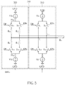
- FIG. 5 is a diagram illustrating a second implementation of the driver circuit 100 shown in FIG. 1 .
- the architecture of the driver circuit 500 is based on that of the driver circuit 200 shown in FIG. 2 , wherein the main difference is the circuit topology of the voltage mode drive unit.
- the driver circuit 500 may include the output terminals T 1 and T 2 shown in FIG. 1 , the current mode drive unit 210 shown in FIG.2 , and a voltage mode drive unit 520.
- the voltage mode drive unit 520 may be used to implement the voltage mode drive unit 120 shown in FIG. 1 .
- the voltage mode drive unit 520 may include the switches S V1 -S V4 shown in FIG. 2 , a plurality of voltage sources VS 0 and VS 0 ', and a plurality of impedance elements (implemented by a plurality of resistors R A -R D in this implementation).
- the voltage sources VS 0 and VS 0 ' may generate the reference voltages V R1 and V R2 shown in FIG. 1 , respectively.
- the resistor R A is coupled between a node N A and the output terminal T 1
- the resistor R B is coupled between a node N B and the output terminal T 2
- the reference voltage V R1 (the voltage source VS 0 ) may be coupled to the node N A through the switch S V1 or coupled to the node N B through the switch S V2 according to the data input DIN 0 .
- the resistor R C is coupled between a node N C and the output terminal T 1
- the resistor R D is coupled between a node N D and the output terminal T 2
- the reference voltage V R2 (the voltage source VS 0 ') may be coupled to the node N C through the switch S V3 or coupled to the node N D through the switch S V4 according to the data input DIN 0 .
- the switch S V1 may be selectively coupled between the reference voltage V R1 and the output terminal T 1 (through the resistor R A )
- the switch S V2 may be selectively coupled between the reference voltage V R1 and the output terminal T 2 (through the resistor R B )
- the switch S V3 may be selectively coupled between the reference voltage V R2 and the output terminal T 1 (through the resistor R C )
- the switch S V4 may be selectively coupled between the reference voltage V R2 and the output terminal T 2 (through the resistor R D ).
- the switch S V1 and the switch S V4 are switched on due to the data input DIN 0
- the switch S V2 and the switch S V3 are switched off
- the switch S V1 and the switch S V4 are switched off due to the data input DIN 0
- the switch S V2 and the switch S V3 are switched on.
- the data signal DP 0 may control switch states of the switches S V1 and S V3 , wherein when one of the switches S V1 and S V3 is switched on, the other of the switches S V1 and S V3 is switched off.
- the data signal DN 0 may control switch states of the switches S V2 and S V4 , wherein when one of the switches S V2 and S V4 is switched on, the other of the switches S V2 and S V4 is switched off. Further, when the switch S V1 is switched on due to the data signal DP 0 , the switch S V2 is switched off due to the data signal DN 0 , and when the switch S V1 is switched off due to the data signal DP 0 , the switch S V2 is switched on due to the data signal DN 0 .
- FIG. 6 is a diagram illustrating an exemplary output operation of the driver circuit 500 shown in FIG. 5
- FIG. 7 is a diagram illustrating another exemplary output operation of the driver circuit 500 shown in FIG. 5 .
- the aforementioned architecture and switch control signals of the voltage mode drive unit 520 are for illustrative purposes, and are not meant to be limitations of the present invention.
- the switches S V1 and S V2 (or the switches S V3 and S V4 ) may be replaced by a three-way switch, thus allowing the reference voltage V R1 to be coupled to one of the node N A and the node N B according to the data input DIN 0 , and allowing the reference voltage V R2 to be coupled to one of the node N C and the node N D according to the data input DIN 0 .
- the reference voltage V R1 and the reference voltage V R2 may be directly/indirectly coupled to the corresponding output terminals through other circuit topologies.
- a voltage mode drive unit may couple the reference voltage V R1 to one of the output terminal T 1 and the output terminal T 2 and couple the reference voltage V R2 to the other of the output terminal T 1 and the output terminal T 2 according to the data input DIN 0 , other variations and modifications fall within the spirit and scope of the present invention.
- FIG. 8 is a first alternative design of the driver circuit 500 shown in FIG. 5 , wherein the driver circuit 800 employs a voltage regulator 822 and a voltage regulator 824 to generate the reference voltage V R1 and the reference voltage V R2 , respectively.
- FIG. 8 is a first alternative design of the driver circuit 500 shown in FIG. 5 , wherein the driver circuit 800 employs a voltage regulator 822 and a voltage regulator 824 to generate the reference voltage V R1 and the reference voltage V R2 , respectively.
- FIG. 9 is a second alternative design of the driver circuit 500 shown in FIG. 5 , wherein the driver circuit 900 employs a resistor R M and a resistor R N to replace the voltage source VS 0 and the voltage source VS 0 ', respectively.
- the resistor R M is coupled to the DC power VDD.
- the driver circuit 900 uses the DC power VDD and a ground voltage as the reference voltage V R1 and the reference voltage V R2 , respectively.
- FIG. 10 is a third alternative design of the driver circuit 500 shown in FIG. 5 , wherein the driver circuit 1000 may directly couple the switches S V1 and S V2 to the DC power VDD, and directly couple the switches S V3 and S V4 to the reference voltage node GND.
- FIG. 11 is a fourth alternative design of the driver circuit 500 shown in FIG. 5 , wherein the driver circuit 1100 employs a voltage regulator 1122 to replace the voltage source VS 0 shown in FIG. 5 , and directly couple the switches S V3 and S V4 to the reference voltage node GND. Specifically, the driver circuit 1100 employs the voltage regulator 1122 to generate the reference voltage V R1 , and uses a ground voltage as the reference voltage V R2 shown in FIG. 5 .
- the voltage source VS A /VS B used for providing the reference voltage V R1 shown in FIG. 2 may be implemented by other voltage generation architectures (e.g. the voltage generation architectures shown in FIGS. 8-11 ), and/or the voltage source VS C /VS D used for providing the reference voltage V R2 shown in FIG. 2 may be implemented by other voltage generation architectures (e.g. the voltage generation architectures shown in FIGS. 8-11 ).
- the driver circuit 1002 may directly couple the switches S V1 and S V2 to the DC power VDD to provide a reference voltage, and directly couple the switches S V3 and S V4 to the reference voltage node GND to provide another reference voltage.
- the driver circuit 800/900/1000/1100/1200 after reading above paragraphs directed to FIGS. 1-7 , similar description is not repeated here for brevity.
- the aforementioned voltages supplied to the current mode drive unit and the voltage mode drive unit are not meant to be limitations of the present invention.
- a voltage supplied to the current mode drive unit may be different from a voltage supplied to the voltage mode drive unit.
- the proposed voltage mode drive unit may switch the output terminals T 1 and T 2 (or two terminals of the termination resistor R T ) to corresponding voltage sources according to a data logic to be outputted, respectively, and the proposed current mode drive unit may selectively output the reference current to the output terminal T 1 /T 2 (or one terminal of the termination resistor R T ) according to the data logic to be outputted, thus avoiding/reducing unnecessary power consumption.
- the proposed driver control scheme may increase an output swing of a driver circuit. Further, the proposed driver control scheme described above may be employed in not only a differential driver structure but also a single-ended driver structure. Further description is provided below.
- FIG. 13 is a block diagram illustrating an exemplary driver circuit according to another embodiment of the present invention.
- the architecture of the driver circuit 1300 is based on the architecture of the driver 100 shown in FIG. 1 , wherein the main difference is that the driver circuit 1300 employs a single-ended structure.
- the driver circuit 1300 may receive the data input DIN 0 and generate an output signal S OUT ' to a termination element (implemented by a termination resistor R S in this embodiment) according to the data input DIN 0 .
- the driver circuit 100 may be employed in a transmitter (not shown in FIG. 1 ), and the termination resistor R S (or a load resistor) may be located in a receiver (not shown in FIG.
- the driver circuit 1300 may include an output terminals T S , a current mode drive unit 1310 and a voltage mode drive unit 1320.
- the output signal S OUT ' may be regarded as a voltage at the output terminal T S , and correspond to an output data logic (e.g. a logic "1" corresponding to a high voltage or a logic "0" corresponding to a low voltage).
- the voltage mode drive unit 1320 is coupled to the output terminal T S , and is arranged for coupling one of the reference voltage V R1 and the reference voltage V R2 (different from the reference voltage V R1 ) to the output terminal T S according to the data input DIN 0 .
- one of the reference voltage V R1 and the reference voltage V R2 may be provided for the output terminal T S , so that the output terminal T S may have different electric potentials to provide corresponding output data logics required by the receiver.
- the current mode drive unit 1310 is coupled to the output terminal T S , and is arranged for generating the reference current I R , wherein the current mode drive unit 1310 may selectively output the reference current I R from the output terminal T S to the termination resistor R S according to the data input DIN 0 . Specifically, when the current mode drive unit 1310 outputs the reference current I R , the current mode drive unit 1310 may steer the reference current I R to flow into the termination resistor R S such that the reference current I R outputted from the current mode drive unit 1310 flows through the termination resistor R S and is used as at least a portion of a current flowing through the termination resistor R S .
- a maximum single-ended output level is limited to one half a supply voltage level.
- the driver circuit 1300 may increase an electric potential of the output terminal T S (e.g. greater than one half a supply voltage level), thereby increasing an output swing while maintaining a low supply voltage level.
- the current mode drive unit 1310 may selectively receive the reference current I R through the output terminal T S according to the data input DIN 0 .
- the current mode drive unit 1310 may output the reference current I R from the output terminal T S according to the data input DIN 0 .
- a voltage of the output terminal T S is increased due to the reference current I R flowing through the termination resistor R S .
- the output signal S OUT ' may correspond to a specific output data logic (e.g. a logic "1").
- the current mode drive unit 1310 may receive the reference current I R through the output terminal T S according to the data input DIN 0 .
- the voltage of the output terminal T S may be decreased due to the reference current I R flowing into the current mode drive unit 1310.
- the output signal S OUT ' may correspond to another specific output data logic (e.g. a logic "0"). Since a voltage level corresponding to the specific output data logic is increased (and/or decreased) due to a voltage drop across the termination resistor R S , a high output swing can be obtained without the need for a high supply voltage.
- the voltage mode drive unit 1320 may couple one of the reference voltage V R1 and the reference voltage V R2 according to the data input DIN 0
- the current mode drive unit 1310 may selectively output/receive the reference current I R from the output terminal T S according to the data input DIN 0
- the driver control mechanism employed in the driver circuit 100 shown in FIG. 1 may be applied to the driver circuit 1300, wherein the driver circuit 100 may be regarded as, but is not limited to, a driver circuit employing bridge termination, and the driver circuit 1300 may be regarded as, but is not limited to, a driver circuit employing single-ended termination.
- the control mechanism described in above paragraphs directed to FIGS. 1-12 may be applied to a proposed driver circuit having a single-ended structure.
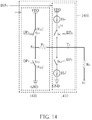
- FIG. 14 is a diagram illustrating an implementation of the driver circuit 1300 shown in FIG. 13 .
- the driver circuit 1400 may include the output terminal T S shown in FIG. 13 , a current mode drive unit 1410 and a voltage mode drive unit 1420, wherein the current mode drive unit 1310 and the voltage mode drive unit 1320 shown in FIG. 13 may be implemented by the current mode drive unit 1410 and the voltage mode drive unit 1420, respectively.
- VDD denotes a direct current (DC) power required by circuit elements
- GND denotes a reference voltage node (e.g. a common ground).
- the current mode drive unit 1410 may include the current source IS 0 and the current sink IS 0 ' shown in FIG. 2 .
- the current source IS 0 may be arranged for generating the reference current I R , and is selectively coupled to the output terminal T S according to the data input DIN 0 .
- the current sink IS 0 ' may be arranged for receiving the reference current I R , and is selectively coupled to the output terminal T S according to the data input DIN 0 , wherein when one of the current source IS 0 and the current sink IS 0 ' is coupled to the output terminal T S according to the data input DIN 0 , the other of the current source IS 0 and the current sink IS 0 ' is not coupled to the output terminal T S .
- the current mode drive unit 1610 may include further include the switches S C1 and S C3 , wherein switch states of the switches S C1 and S C2 are controlled by the data signal DP 0 of the data input DIN 0 .
- the switch S C1 is selectively coupled between the current source IS 0 and the output terminal T S according to the data signal DP 0
- the switch S C2 is selectively coupled between the current sink IS 0 ' and the output terminal T S according to the data signal DP 0 , wherein when the switch S C1 is switched on due to the data signal DP 0 , the switch S C2 is switched off; and when the switch S C1 is switched off due to the data signal DP 0 , the switch S C2 is switched on.
- the switching operations of the switches S C1 and S C3 in this embodiment are identical/similar to those of the switches S C1 and S C3 shown in FIG. 2 .
- the voltage mode drive unit 1420 may include the impedance element (implemented by the resistor R 1 ) and the switches S V1 and S V3 shown in FIG. 2 .
- the resistor R 1 is coupled between a node N S and the output terminal T S , wherein the node N S may be coupled to the DC power VDD (i.e. the reference voltage V R1 ) through the switch S V1 or coupled to a ground voltage (i.e. the reference voltage V R2 ) through the switch S V3 according to the data input DIN 0 .
- the switch S V1 is selectively coupled between the reference voltage V R1 and the output terminal T S (through the resistor R 1 ) according to the data input DIN 0
- the switch S V3 is selectively coupled between the reference voltage V R2 and the output terminal T S (through the resistor R 1 ) according to the data input DIN 0 .
- the switch S V3 when the switch S V1 is switched on due to the data input DIN 0 , the switch S V3 is switched off; when the switch S V1 is switched off due to the data input DIN 0 , the switch S V3 is switched on.
- the data signal DP 0 of the data input DIN 0 may control switch states of the switches S V1 and S V3 , wherein when one of the switches S V1 and S V3 is switched on, the other of the switches S V1 and S V3 is switched off.
- one terminal of the resistor R 1 is coupled to output terminal T S , and another terminal of the resistor R 1 (the node N S ) may be coupled to the DC power VDD through the switch S V1 or coupled to the ground voltage through the switch S V3 according to the data input DIN 0 .
- the switch S V1 when the switch S V1 is switched on according to the data signal DP 0 such that the reference voltage V R1 (the DC power VDD) is coupled to the output terminal T S through the resistor R 1 , the switch S C1 is switched on, and the switches S V3 and S C3 are switched off.
- the reference current I R generated from the current source IS 0 may be outputted from the output terminal T S to the termination resistor R S through the switch S C1 , thus increasing a voltage of the output terminal T S .
- the aforementioned architecture and switch control signal of the voltage mode drive unit 1420 are for illustrative purposes, and are not meant to be limitations of the present invention.
- the switches S V1 and S V3 may be replaced by a three-way switch, thus allowing the node N S to be coupled to one of the DC power VDD and the ground voltage according to the data input DIN 0 .
- the switches S V1 and S V3 and the resistor R 1 shown in FIG. 14 may be replaced by the switches S V1 and S V3 and the resistors R A and R C shown in FIG. 5 .
- the structure of the voltage mode drive unit 1420 may be modified by the voltage mode drive unit 520 shown in FIG. 5 in this alternative design.
- one terminal of the resistor R A is coupled to an output terminal (i.e. the output terminal T S )
- another terminal of the resistor R A is selectively coupled to the DC power VDD through the switch S V1 according to the data input DIN 0
- one terminal of the resistor R B is coupled to the output terminal (i.e.
- the switches S V1 and S V3 and the resistor R 1 shown in FIG. 14 may be replaced by the resistors R A and R C shown in FIG. 5 and a three-way switch (not shown in FIG. 14 ).
- the ground voltage is not coupled to the output terminal T S ;
- the ground voltage is coupled to the output terminal T S through the resistor R B according to the data input DIN 0 , the DC power VDD is not coupled to the output terminal T S .
- the switches S C1 and S C3 may be replaced by a three-way switch, thus allowing the output terminal T S to be coupled to one of the current source IS 0 and the current sink IS 0 ' according to the data input DIN 0 .
- the node N S may be coupled to one of the DC power VDD and the ground voltage according to the data input DIN 0
- one of the current source IS 0 and the current sink IS 0 ' may be coupled to the output terminal T S according to the data input DIN 0
- such alternatives and modifications fall within the scope of the present invention.
- the proposed driver circuit may further use coupling techniques to adjust a voltage level at an output terminal.
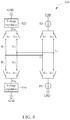
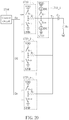
- FIG. 15 is a block diagram illustrating an exemplary driver circuit according to another embodiment of the present invention.
- the architecture of the driver circuit 1500 is based on the architecture of the driver 1300 shown in FIG. 13 , wherein the main difference is that the driver circuit 1500 utilizes a capacitive element 1506 (implemented by a capacitor C S in this embodiment) to adjust a voltage level at the output terminal T S .
- the termination resistor R S when the termination resistor R S is coupled to a ground terminal (the reference voltage VF is implemented by a ground voltage), coupling the capacitor C S between the output terminal T S and the termination resistor R S may prevent the voltage level at the output terminal T S from falling below zero volts.
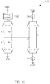
- FIG. 16 is a diagram illustrating an implementation of the driver circuit 1500 shown in FIG. 15 .
- the architecture of the driver circuit 1600 is based on the architecture of the driver 1400 shown in FIG. 14 , wherein the main difference is that the driver circuit 1600 uses the capacitor C S for AC coupling.
- the termination resistor R S is coupled to the common ground GND for illustrative purposes.
- this is not meant to be a limitation of the present invention.
- a magnitude of the DC power VDD is 1 V
- a magnitude of the reference current I R is 1 mA
- each of an impedance value of the resistor R 1 and an impedance value of the termination resistor R S equals to 50 ohm (impedance matching)
- a maximum voltage level at the output terminal T S may be increased to 775 mV (i.e. VDD/2 + VDD/4+ I R xR S /2)
- a minimum voltage level at the output terminal T S may be 225 mV (i.e. VDD/2 - VDD/4 - I R xR S /2).
- the output voltage swing of the output terminal T S may be represented by (VDD/2 + I R xR S ).
- a driver circuit having a differential pair of output terminals may utilize the proposed driver control mechanism to increase the output swing. Please refer to FIG. 12 again.
- the DC power VDD one reference voltage
- the ground voltage another reference voltage
- the switches S V1 and S C1 are switched on according to the data signal DP 0
- the switches S V4 and S C4 are switched on according to the data signal DN 0
- the switches S V3 and S C3 are switched off according to the data signal DP 0
- the switches S V2 and S C2 are switched off according to the data signal DN 0 .
- switches S V1 and S C1 are switched off according to the data signal DP 0
- the switches S V4 and S C4 are switched off according to the data signal DN 0
- the switches S V3 and S C3 are switched on according to the data signal DP 0
- the switches S V2 and S C2 are switched on according to the data signal DN 0 .
- a maximum voltage level at the output terminal T S may be increased to 550 mV (i.e. VDD/2 + I R xR T /2), and a minimum voltage level at the output terminal T S may be -550 mV (i.e. -VDD/2 - I R xR S /2).
- the output voltage swing of the output terminal T S may be represented by (VDD + I R xR S ).
- the proposed driver circuit may obtain an output swing higher than the supply voltage level (i.e. VDD).
- the proposed driver control mechanism may be employed in other differential circuit topologies, such as the driver circuit 500 shown in FIG. 5 , to increase an output swing.
- the driver circuit 500 shown in FIG. 5
- FIGS. 1-16 further description is omitted here for brevity.
- the proposed driver control mechanism may be employed in a multi-level driver.
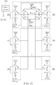
- FIG. 17 is a diagram illustrating an exemplary driver circuit according to an embodiment of the present invention.
- the architecture of the driver circuit shown in FIG. 17 is based on that of the driver circuit 1400 shown in FIG. 14 , and the main difference is that the driver circuit shown in FIG. 17 includes n current mode drive units 1710_1-1710_n and n voltage mode drive units 1720_1-1720_n, wherein n is an integer greater than one.
- a control circuit 1704 which may be implemented by a digital-to-analog converter (DAC), a transmit finite impulse response (FIR) circuit or other types of control circuit.
- DAC digital-to-analog converter
- FIR transmit finite impulse response
- the current mode drive unit 1710_1 and the voltage mode drive unit 1720_1 are controlled by the data signal D1
- the current mode drive unit 1710_2 and the voltage mode drive unit 1720_2 are controlled by the data signal D2, and so on.
- Each current mode drive unit includes a current source (one of current sources IM 1 -IM n ), a current sink (one of current sinks IM 1 '-IM n ') and a set of switches (e.g. switches S C11 -S C13 /S C21 -S C23 /.../S Cn1 -S Cn3 ), and may output a reference current from the output terminal T S to the termination resistor R S according to a corresponding data input (one of the data signals D1-Dn).
- Each voltage mode drive unit includes a set of switches (e.g.
- the n data inputs correspond to a binary code of n bits
- the generated output signal e.g. the voltage level at the output terminal T S
- the n components of the generated output signal have a binary-weighted relationship.
- control circuit 1704 is implemented by a transmit FIR circuit
- different voltage/current mode drive units are used for pre-emphasis and/or de-emphasis, wherein one of the data signals D1-Dn is an advanced signal or a delayed signal relative to another/others of the data signals D1-Dn.
- FIG. 18 is a diagram illustrating an exemplary driver circuit according to another embodiment of the present invention.
- the architecture of the driver circuit shown in FIG. 18 is based on that of the driver circuit shown in FIG. 17 , and the main difference is that the driver circuit shown in FIG. 18 further includes the capacitor C S for AC coupling.
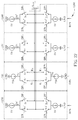
- FIG. 19 is a diagram illustrating an exemplary driver circuit according to another embodiment of the present invention.
- the architecture of the driver circuit shown in FIG. 19 is based on that of the driver circuit 1200 shown in FIG. 12 , and the main difference is that the driver circuit shown in FIG. 19 includes n current mode drive units1910_1-1910_n and n voltage mode drive units 1920_1-1920_n, wherein n is an integer greater than one.
- the driver circuit shown in FIG. 19 generates an output signal to the termination resistor R S according to n data inputs generated from a control circuit 1904, which may be implemented by a digital-to-analog converter (DAC), a transmit finite impulse response (FIR) circuit or other types of control circuit.
- DAC digital-to-analog converter
- FIR transmit finite impulse response
- each of the n data inputs includes a first data signal (one of the data signals D1-Dn) and a second data signal (one of the data signals D1'-Dn'), wherein the first data signal and the second data signal may be inverted with respect to each other, or non-overlapping signals.
- the current mode drive unit 1910_1 and the voltage mode drive unit 1920_1 are controlled by the data signal D1 and the data signal D1'
- the current mode drive unit 1910_2 and the voltage mode drive unit 1920_2 are controlled by the data signal D2 and the data signal D2', and so on.
- Each current mode drive unit includes a current source (one of current sources IM 1 -IM n ), a current sink (one of current sinks IM 1 '-IM n ') and a set of switches (e.g. switches S C11 -S C14 /S C21 -S C24 /.../S Cn1 -S Cn4 ), and may output/receive a reference current from a differential pair of output terminals (having output terminals T S and T S ') according to a corresponding data input (a set of the data signals D1-D1'/D2-D2'/.../Dn-Dn').
- Each voltage mode drive unit includes a set of switches (e.g.
- the n data inputs i.e. the data signals D1-Dn or D1'-Dn'
- the generated output signal may include n components which are generated in response to the n data inputs respectively.
- the n components of the generated output signal have a binary-weighted relationship.
- n 3
- a magnitude of the DC power VDD is 1 V
- a sum of respective magnitudes of reference currents generated from the current sources IM 1 -IM 3 is 1 mA
- a sum of respective inverses of impedance values of the resistors R 11 -R n1 i.e. 1/R 11 +1/R 21 +...+1/R n1
- a sum of respective inverses of impedance values of the resistors R 12 -R n2 i.e.
- 1/R 12 +1/R 22 +...+1/R n2 equals to the inverse of one half the impedance value of the termination resistor R SM , and the impedance value of the termination resistor R SM equals to 100 ohm, the relationship between the binary-weighted code and a differential output (a level difference between the output terminals T S and T S ') is shown in the table below.
- control circuit 1904 is implemented by a transmit FIR circuit
- different voltage/current mode drive units are used for pre-emphasis and/or de-emphasis, wherein one of the n data inputs is an advanced signal or a delayed signal relative to another/others of the n data inputs.
- the data signals D1-Dn are generated by a 3-tap transmit FIR circuit (i.e. n equals to 3) and a weight ratio corresponding to D1-Dn is 5:2:1.
- a magnitude of the DC power VDD is 1 V
- a sum of respective magnitudes of reference currents generated from the current sources IM 1 -IM 3 is 1 mA
- a sum of respective inverses of impedance values of the resistors R 11 -R n1 i.e.
- 1/R 11 +1/R 21 +...+1/R n1 equals to an inverse of one half an impedance value of the termination resistor R SM
- a sum of respective inverses of impedance values of the resistors R 12 -R n2 i.e. 1/R 12 +1/R 22 +...+1/R n2
- the impedance value of the termination resistor R SM equals to 100 ohm
- the number of the current mode drive units and the number of the voltage mode drive units may be different.
- high speed application may use less current mode drive units to increase bandwidth.
- FIG. 20 illustrates an example where the number of the current mode drive units may be less than the number of the voltage mode drive units in a single-ended driver structure
- FIG. 21 illustrates an example where the number of the current mode drive units may be less than the number of the voltage mode drive units in a differential driver structure.
- the proposed driver circuit is employed in an equalizer architecture in order to improve quality of signal transmission
- the proposed current mode drive unit may be utilized to increase design flexibility.
- An exemplary implementation of a three-tap finite impulse response (FIR) equalizer is given in the following for description of the proposed equalizer architecture.
- FIR finite impulse response
- FIG. 22 is a diagram illustrating an exemplary driver circuit according to an embodiment of the present invention.
- the architecture of the driver circuit 1200 is based on that of the driver circuit 500 shown in FIG. 5 , wherein the main difference is that the driver circuit 1200 may further include a current mode drive unit 1230 and a current mode drive unit 1240 for pre-emphasis and/or de-emphasis.
- the driver circuit 1200 may receive a plurality of data inputs DIN 0 , DIN -1 and DIN 1 , and accordingly generate the output signal S OUT , wherein the data input DIN -1 is an advanced data input relative to the data input DIN 0 , and the data input DIN 1 is a delayed data input relative to the data input DIN 0 .
- the current mode drive unit 1230 is coupled to the output terminal T 1 and the output terminal T 2 (a pair of differential output terminals), and is arranged for generating a reference current I R ', outputting the reference current I R ' from one of the output terminal T 1 and the output terminal T 2 according to the data input DIN -1 , and receiving the reference current I R ' from the other of the output terminal T 1 and the output terminal T 2 according to the data input DIN -1 .
- the current mode drive unit 1240 is coupled to the output terminal T 1 and the output terminal T 2 , and is arranged for generating a reference current I R ", outputting the reference current I R " from one of the output terminal T 1 and the output terminal T 2 according to the data input DIN 1 , and receiving the reference current I R " from the other of the output terminal T 1 and the output terminal T 2 according to the data input DIN 1 .
- the architecture of the current mode drive unit 1230 is based on that of the current mode drive unit 210
- the architecture of the current mode drive unit 1240 is based on that of the current mode drive unit 210.
- the current mode drive unit 1230 may include a current source IS -1 , a current sink IS -1 ' and a plurality of switches S C1 '-S C4 '
- the current mode drive unit 1240 may include a current source IS 1 , a current sink IS 1 ' and a plurality of switches S C1 "-S C4 ".
- the data input DIN -1 may include a data signal DP -1 and a data signal DN -1 , wherein the data signal DP -1 and the data signal DN -1 may be inverted with respect to each other, or non-overlapping signals.
- the data signal DP -1 may control switch states of the switches S C1 ' and S C3 '
- the data signal DN -1 may control switch states of the switches S 2 ' and S C4 ', wherein the data signal DP -1 is an advanced signal relative to the data signal DP 0 (e.g. advanced by one bit period), and the data signal DN -1 is an advanced signal relative to the data signal DN 0 (e.g. advanced by one bit period).
- the data input DIN 1 may include a data signal DP 1 and a data signal DN 1 , wherein the data signal DP 1 and the data signal DN 1 may be inverted with respect to each other, or non-overlapping signals.
- the data signal DP 1 may control switch states of the switches S C1 " and S C3 "
- the data signal DN 1 may control switch states of the switches S C2 " and S C4 ", wherein the data signal DP 1 is an delayed signal relative to the data signal DP 0 (e.g. delayed by one bit period), and the data signal DN 1 is a delayed signal relative to the data signal DN 0 (e.g. delayed by one bit period).
- the switches S C2 ' and S C4 ' coupled to the output terminal T 1 may be controlled by the data signal DN -1 (the advanced signal relative to the data signal DN 0 ), the switches S C2 " and S C4 " coupled to the output terminal T 1 may be controlled by the data signal DN 1 (the delayed signal relative to the data signal DN 0 ), the switches S C1 ' and S C3 ' coupled to the output terminal T 2 may be controlled by the data signal DP -1 (the advanced signal relative to the data signal DP 0 ), and the switches S C1 " and S C3 " coupled to the output terminal T 2 may be controlled by the data signal DP 1 (the delayed signal relative to the data signal DP 0 ).
- respective magnitudes of the reference currents I R ' and I R " may be adjusted according to design considerations.
- a person skilled in the field of transmitter equalizers should understand the operations of the driver circuit 1200 employed in a three-tap FIR equalizer after reading above paragraphs directed to FIGS. 1 - 7 , further description is omitted here for brevity.
- channel loss compensation may be achieved by merely adding the current mode drive units 1230 and 1240 without modifying original circuit elements (e.g. the current mode drive unit 210 and/or the voltage mode drive unit 520), which means that the proposed driver architecture may have high design flexibility.
- an N-tap FIR equalizer may be easily implemented using the proposed driver architecture, wherein N is a positive integer.
- the current mode drive unit 1230 or the current mode drive unit 1240 may be optional.
- other current mode drive unit(s) may be added to implement an equalizer.
- the current mode drive unit 210/1230/1240 may be replaced by a current mode drive unit which is implemented based on the operations of the current mode drive unit 110 shown in FIG.
- the voltage mode drive unit 520 may be replaced by a voltage mode drive unit which is implemented based on the operations of the voltage mode drive unit 120 shown in FIG. 1 .
- the driver circuit 200 shown in FIG. 2 may be used to implement the N-tap FIR equalizer.
- the proposed driver circuit may not only reduce power loss but also have high design flexibility. Additionally, as the proposed driver circuit may decrease a drive current, a size of a switch device may be reduced, thus decreasing a load impedance seen by a differential output pair and reducing parasitic capacitance. Moreover, the proposed driver circuit may increase an output swing while maintaining a low supply voltage level.
Landscapes
- Engineering & Computer Science (AREA)
- Computer Hardware Design (AREA)
- Physics & Mathematics (AREA)
- Computing Systems (AREA)
- General Engineering & Computer Science (AREA)
- Mathematical Physics (AREA)
- Theoretical Computer Science (AREA)
- Logic Circuits (AREA)
- Dc Digital Transmission (AREA)
Applications Claiming Priority (2)
| Application Number | Priority Date | Filing Date | Title |
|---|---|---|---|
| US201562260723P | 2015-11-30 | 2015-11-30 | |
| US15/069,880 US9871539B2 (en) | 2013-07-16 | 2016-03-14 | Driver circuit for signal transmission and control method of driver circuit |
Publications (1)
| Publication Number | Publication Date |
|---|---|
| EP3174209A1 true EP3174209A1 (de) | 2017-05-31 |
Family
ID=56014819
Family Applications (1)
| Application Number | Title | Priority Date | Filing Date |
|---|---|---|---|
| EP16169102.7A Withdrawn EP3174209A1 (de) | 2015-11-30 | 2016-05-11 | Treiberschaltung zur signalübertragung |
Country Status (2)
| Country | Link |
|---|---|
| EP (1) | EP3174209A1 (de) |
| CN (1) | CN106817119A (de) |
Families Citing this family (4)
| Publication number | Priority date | Publication date | Assignee | Title |
|---|---|---|---|---|
| CN108599750A (zh) * | 2018-01-23 | 2018-09-28 | 电子科技大学 | 一种SiC-BJT的单电源驱动电路 |
| CN110719047B (zh) * | 2019-10-24 | 2020-09-11 | 杭州雄迈集成电路技术股份有限公司 | 一种新型低功耗mipi电流模驱动装置 |
| US11411574B2 (en) * | 2020-04-06 | 2022-08-09 | M31 Technology Corporation | Clock and data recovery circuit with proportional path and integral path, and multiplexer circuit for clock and data recovery circuit |
| US12255436B2 (en) * | 2020-12-16 | 2025-03-18 | Macom Technology Solutions Holdings, Inc. | PAM driver with distributed modulation current setpoint feedback |
Citations (4)
| Publication number | Priority date | Publication date | Assignee | Title |
|---|---|---|---|---|
| US6812733B1 (en) * | 2002-08-02 | 2004-11-02 | Pmc-Sierra, Inc. | High-efficiency mixed voltage/current mode output driver |
| GB2497145A (en) * | 2011-11-29 | 2013-06-05 | Texas Instruments Ltd | Power efficient transmitter with a high voltage swing for sending high speed data along long backplanes |
| US8487654B1 (en) * | 2012-02-29 | 2013-07-16 | Taiwan Semiconductor Manufacturing Co., Ltd. | Voltage mode driver with current booster (VMDCB) |
| US20150022243A1 (en) * | 2013-07-16 | 2015-01-22 | Mediatek Inc. | Driver circuit for signal transmission and control method of driver circuit |
Family Cites Families (6)
| Publication number | Priority date | Publication date | Assignee | Title |
|---|---|---|---|---|
| US7109759B2 (en) * | 2003-05-23 | 2006-09-19 | Avago Technologies Fiber Ip (Singapore) Pte.Ltd. | Voltage mode current-assisted pre-emphasis driver |
| CN100488053C (zh) * | 2005-09-05 | 2009-05-13 | 中兴通讯股份有限公司 | 一种低压差分信号驱动器电路 |
| CN102025365B (zh) * | 2009-09-18 | 2012-08-22 | 复旦大学 | 一种降低电压摆幅驱动器 |
| US8415979B2 (en) * | 2010-11-04 | 2013-04-09 | Mediatek Inc. | Differential driver with calibration circuit and related calibration method |
| CN104300956A (zh) * | 2013-07-16 | 2015-01-21 | 联发科技股份有限公司 | 驱动电路以及控制驱动电路的方法 |
| US9362917B1 (en) * | 2014-11-24 | 2016-06-07 | Via Alliance Semiconductor Co., Ltd. | Low voltage differential signaling (LVDS) driving circuit |
-
2016
- 2016-05-11 EP EP16169102.7A patent/EP3174209A1/de not_active Withdrawn
- 2016-05-24 CN CN201610351808.3A patent/CN106817119A/zh not_active Withdrawn
Patent Citations (4)
| Publication number | Priority date | Publication date | Assignee | Title |
|---|---|---|---|---|
| US6812733B1 (en) * | 2002-08-02 | 2004-11-02 | Pmc-Sierra, Inc. | High-efficiency mixed voltage/current mode output driver |
| GB2497145A (en) * | 2011-11-29 | 2013-06-05 | Texas Instruments Ltd | Power efficient transmitter with a high voltage swing for sending high speed data along long backplanes |
| US8487654B1 (en) * | 2012-02-29 | 2013-07-16 | Taiwan Semiconductor Manufacturing Co., Ltd. | Voltage mode driver with current booster (VMDCB) |
| US20150022243A1 (en) * | 2013-07-16 | 2015-01-22 | Mediatek Inc. | Driver circuit for signal transmission and control method of driver circuit |
Also Published As
| Publication number | Publication date |
|---|---|
| CN106817119A (zh) | 2017-06-09 |
Similar Documents
| Publication | Publication Date | Title |
|---|---|---|
| US9871539B2 (en) | Driver circuit for signal transmission and control method of driver circuit | |
| US9312846B2 (en) | Driver circuit for signal transmission and control method of driver circuit | |
| US10728060B2 (en) | Two-step feed-forward equalizer for voltage-mode transmitter architecture | |
| US9590595B2 (en) | Driver circuit with feed-forward equalizer | |
| US10033412B2 (en) | Impedance and swing control for voltage-mode driver | |
| US9746864B1 (en) | Fast transient low drop-out voltage regulator for a voltage-mode driver | |
| US9853642B1 (en) | Data-dependent current compensation in a voltage-mode driver | |
| US7528635B2 (en) | Multitap fractional baud period pre-emphasis for data transmission | |
| US9590610B2 (en) | Driver circuit for signal transmission and control method of driver circuit | |
| KR102112199B1 (ko) | 데이터 전송 채널을 이퀄라이징하기 위한 시스템 및 이를 포함하는 디스플레이 | |
| US20160182080A1 (en) | High-speed, low-power reconfigurable voltage-mode dac-driver | |
| JP2010518749A (ja) | 高速低電力差動受信機RobertE.PalmerJohnW.Poulton | |
| WO2018026578A1 (en) | Impedance and swing control for voltage-mode driver | |
| US20120049897A1 (en) | Output buffer circuit and semiconductor device | |
| EP3174209A1 (de) | Treiberschaltung zur signalübertragung | |
| US10171273B2 (en) | Decision feedback equalizer and interconnect circuit | |
| CN104300956A (zh) | 驱动电路以及控制驱动电路的方法 | |
| JP7738300B2 (ja) | 駆動モジュール | |
| US9210011B2 (en) | Push-pull source-series terminated transmitter apparatus and method | |
| CN106027055A (zh) | 一种低功耗两步式闪烁型模数转换器 | |
| Hu et al. | An R2R-DAC-based architecture for equalization-equipped voltage-mode PAM-4 wireline transmitter design | |
| CN115086117A (zh) | 一种判决反馈方法及判决反馈均衡器 | |
| US10418976B1 (en) | Charge steering transmitter | |
| US10389315B2 (en) | Three-input continuous-time amplifier and equalizer for multi-level signaling | |
| JP2013009157A (ja) | 情報処理装置および情報処理装置の制御方法 |
Legal Events
| Date | Code | Title | Description |
|---|---|---|---|
| PUAI | Public reference made under article 153(3) epc to a published international application that has entered the european phase |
Free format text: ORIGINAL CODE: 0009012 |
|
| AK | Designated contracting states |
Kind code of ref document: A1 Designated state(s): AL AT BE BG CH CY CZ DE DK EE ES FI FR GB GR HR HU IE IS IT LI LT LU LV MC MK MT NL NO PL PT RO RS SE SI SK SM TR |
|
| AX | Request for extension of the european patent |
Extension state: BA ME |
|
| 17P | Request for examination filed |
Effective date: 20170727 |
|
| RBV | Designated contracting states (corrected) |
Designated state(s): AL AT BE BG CH CY CZ DE DK EE ES FI FR GB GR HR HU IE IS IT LI LT LU LV MC MK MT NL NO PL PT RO RS SE SI SK SM TR |
|
| 17Q | First examination report despatched |
Effective date: 20190617 |
|
| STAA | Information on the status of an ep patent application or granted ep patent |
Free format text: STATUS: THE APPLICATION IS DEEMED TO BE WITHDRAWN |
|
| 18D | Application deemed to be withdrawn |
Effective date: 20200609 |