EP3174372B1 - Structure de prévention de pic électrostatique - Google Patents
Structure de prévention de pic électrostatique Download PDFInfo
- Publication number
- EP3174372B1 EP3174372B1 EP15823941.8A EP15823941A EP3174372B1 EP 3174372 B1 EP3174372 B1 EP 3174372B1 EP 15823941 A EP15823941 A EP 15823941A EP 3174372 B1 EP3174372 B1 EP 3174372B1
- Authority
- EP
- European Patent Office
- Prior art keywords
- circuit board
- printed circuit
- flexible printed
- touch panel
- electrostatic surge
- Prior art date
- Legal status (The legal status is an assumption and is not a legal conclusion. Google has not performed a legal analysis and makes no representation as to the accuracy of the status listed.)
- Not-in-force
Links
Images

Classifications
-
- H—ELECTRICITY
- H05—ELECTRIC TECHNIQUES NOT OTHERWISE PROVIDED FOR
- H05F—STATIC ELECTRICITY; NATURALLY-OCCURRING ELECTRICITY
- H05F3/00—Carrying-off electrostatic charges
- H05F3/02—Carrying-off electrostatic charges by means of earthing connections
-
- B—PERFORMING OPERATIONS; TRANSPORTING
- B60—VEHICLES IN GENERAL
- B60K—ARRANGEMENT OR MOUNTING OF PROPULSION UNITS OR OF TRANSMISSIONS IN VEHICLES; ARRANGEMENT OR MOUNTING OF PLURAL DIVERSE PRIME-MOVERS IN VEHICLES; AUXILIARY DRIVES FOR VEHICLES; INSTRUMENTATION OR DASHBOARDS FOR VEHICLES; ARRANGEMENTS IN CONNECTION WITH COOLING, AIR INTAKE, GAS EXHAUST OR FUEL SUPPLY OF PROPULSION UNITS IN VEHICLES
- B60K35/00—Instruments specially adapted for vehicles; Arrangement of instruments in or on vehicles
- B60K35/10—Input arrangements, i.e. from user to vehicle, associated with vehicle functions or specially adapted therefor
-
- B—PERFORMING OPERATIONS; TRANSPORTING
- B60—VEHICLES IN GENERAL
- B60K—ARRANGEMENT OR MOUNTING OF PROPULSION UNITS OR OF TRANSMISSIONS IN VEHICLES; ARRANGEMENT OR MOUNTING OF PLURAL DIVERSE PRIME-MOVERS IN VEHICLES; AUXILIARY DRIVES FOR VEHICLES; INSTRUMENTATION OR DASHBOARDS FOR VEHICLES; ARRANGEMENTS IN CONNECTION WITH COOLING, AIR INTAKE, GAS EXHAUST OR FUEL SUPPLY OF PROPULSION UNITS IN VEHICLES
- B60K35/00—Instruments specially adapted for vehicles; Arrangement of instruments in or on vehicles
- B60K35/20—Output arrangements, i.e. from vehicle to user, associated with vehicle functions or specially adapted therefor
- B60K35/21—Output arrangements, i.e. from vehicle to user, associated with vehicle functions or specially adapted therefor using visual output, e.g. blinking lights or matrix displays
- B60K35/22—Display screens
-
- B—PERFORMING OPERATIONS; TRANSPORTING
- B60—VEHICLES IN GENERAL
- B60R—VEHICLES, VEHICLE FITTINGS, OR VEHICLE PARTS, NOT OTHERWISE PROVIDED FOR
- B60R16/00—Electric or fluid circuits specially adapted for vehicles and not otherwise provided for; Arrangement of elements of electric or fluid circuits specially adapted for vehicles and not otherwise provided for
- B60R16/02—Electric or fluid circuits specially adapted for vehicles and not otherwise provided for; Arrangement of elements of electric or fluid circuits specially adapted for vehicles and not otherwise provided for electric constitutive elements
-
- H—ELECTRICITY
- H02—GENERATION; CONVERSION OR DISTRIBUTION OF ELECTRIC POWER
- H02H—EMERGENCY PROTECTIVE CIRCUIT ARRANGEMENTS
- H02H9/00—Emergency protective circuit arrangements for limiting excess current or voltage without disconnection
- H02H9/04—Emergency protective circuit arrangements for limiting excess current or voltage without disconnection responsive to excess voltage
- H02H9/045—Emergency protective circuit arrangements for limiting excess current or voltage without disconnection responsive to excess voltage adapted to a particular application and not provided for elsewhere
-
- H—ELECTRICITY
- H05—ELECTRIC TECHNIQUES NOT OTHERWISE PROVIDED FOR
- H05K—PRINTED CIRCUITS; CASINGS OR CONSTRUCTIONAL DETAILS OF ELECTRIC APPARATUS; MANUFACTURE OF ASSEMBLAGES OF ELECTRICAL COMPONENTS
- H05K1/00—Printed circuits
- H05K1/02—Details
- H05K1/0277—Bendability or stretchability details
- H05K1/028—Bending or folding regions of flexible printed circuits
-
- H—ELECTRICITY
- H05—ELECTRIC TECHNIQUES NOT OTHERWISE PROVIDED FOR
- H05K—PRINTED CIRCUITS; CASINGS OR CONSTRUCTIONAL DETAILS OF ELECTRIC APPARATUS; MANUFACTURE OF ASSEMBLAGES OF ELECTRICAL COMPONENTS
- H05K1/00—Printed circuits
- H05K1/02—Details
- H05K1/14—Structural association of two or more printed circuits
- H05K1/147—Structural association of two or more printed circuits at least one of the printed circuits being bent or folded, e.g. by using a flexible printed circuit
-
- B—PERFORMING OPERATIONS; TRANSPORTING
- B60—VEHICLES IN GENERAL
- B60K—ARRANGEMENT OR MOUNTING OF PROPULSION UNITS OR OF TRANSMISSIONS IN VEHICLES; ARRANGEMENT OR MOUNTING OF PLURAL DIVERSE PRIME-MOVERS IN VEHICLES; AUXILIARY DRIVES FOR VEHICLES; INSTRUMENTATION OR DASHBOARDS FOR VEHICLES; ARRANGEMENTS IN CONNECTION WITH COOLING, AIR INTAKE, GAS EXHAUST OR FUEL SUPPLY OF PROPULSION UNITS IN VEHICLES
- B60K2360/00—Indexing scheme associated with groups B60K35/00 or B60K37/00 relating to details of instruments or dashboards
- B60K2360/143—Touch sensitive instrument input devices
- B60K2360/1438—Touch screens
-
- B—PERFORMING OPERATIONS; TRANSPORTING
- B60—VEHICLES IN GENERAL
- B60K—ARRANGEMENT OR MOUNTING OF PROPULSION UNITS OR OF TRANSMISSIONS IN VEHICLES; ARRANGEMENT OR MOUNTING OF PLURAL DIVERSE PRIME-MOVERS IN VEHICLES; AUXILIARY DRIVES FOR VEHICLES; INSTRUMENTATION OR DASHBOARDS FOR VEHICLES; ARRANGEMENTS IN CONNECTION WITH COOLING, AIR INTAKE, GAS EXHAUST OR FUEL SUPPLY OF PROPULSION UNITS IN VEHICLES
- B60K2360/00—Indexing scheme associated with groups B60K35/00 or B60K37/00 relating to details of instruments or dashboards
- B60K2360/40—Hardware adaptations for dashboards or instruments
- B60K2360/42—Circuit board features
-
- H—ELECTRICITY
- H05—ELECTRIC TECHNIQUES NOT OTHERWISE PROVIDED FOR
- H05K—PRINTED CIRCUITS; CASINGS OR CONSTRUCTIONAL DETAILS OF ELECTRIC APPARATUS; MANUFACTURE OF ASSEMBLAGES OF ELECTRICAL COMPONENTS
- H05K9/00—Screening of apparatus or components against electric or magnetic fields
Definitions
- the present invention relates to electrostatic surge prevention structure capable of allowing static electricity coming in through a gap in a casing of an in-vehicle device to escape to ground and preventing electrostatic surge from occurring.
- a circuit board part is formed on a glass substrate of a liquid crystal display panel in a display device, and a display control device is connected to a driver IC provided in the circuit board part via a flexible printed circuit board.
- a shielding metal foil is pasted on the flexible printed circuit board, a metal foil tape is pasted on the shielding metal foil, and moreover, the metal foil tape is pasted on a frame body of the liquid crystal display device. Thereby, the shielding metal foil is electrically connected to the frame body via the metal foil tape, and thus, the structure for absorbing radiation noise generated from the flexible printed circuit board is formed.
- Document JP 2009 158808 discloses an electrostatic surge prevention structure according to the preamble of claim 1.
- Document CN 202 121 863 U relates to an anti-interference flexible printed circuit which includes an insulating substrate layer, a plurality of conductive grounding bodies which can be connected with a ground wire in a circuit, and a plurality of conductive contact bodies which are electrically connected mutually.
- Patent Literature 1 Japanese Patent Laid-Open No. 2005-49774
- static electricity for example, generated on the liquid crystal display panel side can also be not to come inside the liquid crystal display device and not to damage an IC included in the display control device or the like.
- the static electricity can be allowed to escape to the frame body which is the ground side via the shielding metal foil and the metal foil tape.
- the present invention is devised in view of the aforementioned circumstances and an object thereof is to provide an electrostatic surge prevention structure capable of improving resistance against electrostatic surge, reducing costs and processes, and saving spaces.
- the present invention is characterized in that a flexible printed circuit board connected to a circuit board contained in an electronic device is provided at a position corresponding to a gap, between two members, appearing in the electronic device, and the flexible printed circuit board has two layers of conductor parts, surfaces of these conductor parts are covered with insulative coats, an exposed part through which one of the conductor parts is externally exposed is formed at a portion opposing the gap by peeling off the insulative coat, and the conductor part having the exposed part is grounded.
- the exposed part may be provided at a position closer to the gap than a connecting part provided in an end part of the flexible printed circuit board. According to this configuration, by providing the exposed part at the position closer to the gap, static electricity can easily reach the exposed part from the gap, and electrostatic surge can be prevented from occurring.
- the exposed part may undergo plating with conductivity. According to this configuration, the plating can prevent corrosion of the exposed part.
- the two members may be constituted of a front casing constituting a front part of the electronic device for being implemented in a vehicle, and a touch panel attached to the front casing, and the flexible printed circuit board may connect the touch panel to a touch panel control circuit provided in the circuit board.
- electrostatic surge due to static electricity flowing from an occupant operating the touch panel can be prevented from occurring, and damage to an IC or the like of the touch panel control circuit can be prevented.
- a flexible printed circuit board connected to a circuit board contained in an electronic device is provided at a position corresponding to a gap, between two members, appearing in the electronic device, and the flexible printed circuit board has two layers of conductor parts, surfaces of these conductor parts are covered with insulative coats, an exposed part through which one of the conductor parts is externally exposed is formed at a portion opposing the gap by peeling off the insulative coat, and the conductor part having the exposed part is grounded.
- static electricity coming into the electronic device through the gap can be allowed to escape to the ground via the exposed part, and electrostatic surge can be prevented from occurring. Since static electricity is allowed to escape using the conductor part of the existing flexible printed circuit board, a structure for preventing electrostatic surge or processes or spaces for providing the structure are not particularly needed but resistance against electrostatic surge can be improved while costs and processes are reduced and spaces are saved.
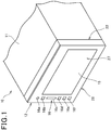
- FIG. 1 is a perspective view of an in-vehicle device 10 employing an electrostatic surge prevention structure of the present invention.
- the in-vehicle device 10 includes a substantially rectangular solid-shaped device main body 11 and a display device 12 which is provided on the front side of the device main body 11 and can be operated through touch operation.
- the in-vehicle device 10 is an in-vehicle electronic device such as an audio device playing back CDs, DVDs and the like and a navigation device searching for paths to designated destinations, and is implemented by being embedded in an accommodation space provided on an instrument panel or the like of a vehicle.
- the display device 12 includes a touch screen 15 undergoing input operation by touching an arbitrary position thereon with a finger, and a touch switch part 16 for performing predetermined operations by touching predetermined positions thereon with a finger.
- the touch switch part 16 includes a plurality of touch switches 16a, 16b, 16c, 16d, 16e and 16f.
- FIG. 2 is an exploded perspective view showing the display device 12.
- the display device 12 includes a touch panel assembly 21, a front casing 22, a liquid crystal module 23, a liquid crystal holder 24 and a control printed circuit board 26 in the order from the front side.
- the touch panel assembly 21 includes a touch panel 27 and a decorative panel 28 pasted on the front face of the touch panel 27.
- the touch panel 27 is a panel which is overlapped and disposed on the front face of the liquid crystal module 23 and employs a touch detection system such as a resistance film system and a capacitance system, and undergoes predetermined input operation by touching representation on a liquid crystal screen of the liquid crystal module 23.
- the decorative panel 28 forms the touch screen 15 and the touch switch part 16 by being pasted on the front face of the touch panel 27, and moreover, covers the pattern of a drive circuit formed in a periphery part of the touch panel 27.
- the touch panel assembly 21 is attached, and in the interior thereof, the liquid crystal module 23, the liquid crystal holder 24 and the control printed circuit board 26 are contained.
- the liquid crystal module 23 is constituted of a liquid crystal display, a drive circuit board driving the liquid crystal display, a backlight, and the like.
- the liquid crystal holder 24 retains the liquid crystal module 23 and is attached to the front casing 22.
- the control printed circuit board 26 is a circuit board having a touch panel control circuit disposed close to the liquid crystal holder 24.
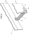
- FIG. 3 is a perspective view showing a flexible printed circuit board 31 and its periphery.
- a pattern formed part 27a in which a conductive wire pattern for outputting information of a touched position is formed is provided on an edge part of the rear face of the touch panel 27, a pattern formed part 27a in which a conductive wire pattern for outputting information of a touched position is formed is provided. Onto the pattern formed part 27a, one end part 31a of the flexible printed circuit board 31 is connected by bonding.
- the other end part 31b thereof is detachably connected to a connector 34 provided on the control printed circuit board 26. Thereby, a signal corresponding to the touch position is sent from the touch panel 27 to the control printed circuit board 26 via the flexible printed circuit board 31, and the touch position is specified.
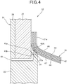
- FIG. 4 is a cross-sectional view showing the touch panel 27, the flexible printed circuit board 31, and their peripheries.
- a gap 41 which is a part of a design is provided.
- the gap 41 can cause a risk that static electricity from the finger touching the touch panel 27 or the decorative panel 28 comes inside the display device 12, and it damages, for example, an IC or the like provided on the control printed circuit board 26 (see FIG. 3 ).
- the flexible printed circuit board 31 is caused to have the following structure, and thereby, the aforementioned problem is solved.
- the flexible printed circuit board 31 is constituted of a base material 42 forming a layer at the center of its thickness, conductor parts 43 and 44 constituted of copper foils or the like provided on both sides of the base material, and insulative coats 46 and 47 respectively covering the conductor parts 43 and 44.
- the base material 42 is composed of a resin material such as polyimide.
- the conductor part 43 is a signal line allowing a signal to flow from the touch panel 27 to the control printed circuit board 26.
- the conductor part 44 is connected to the ground on the control printed circuit board 26 (see FIG. 3 ) side.
- the insulative coats 46 and 47 are formed of colorless or colored, transparent polyimide films, solder resist films or the like.
- the insulative coat 47 on the conductor part 44 side is cut away at the position closest to an opening 41a (specifically, a point 41b at the center of the opening 41a) inside the gap 41 to form a notch part 47a, and thus, an exposed part 44A externally exposed through the notch part 47a appears on the conductor part 44.
- the exposed part 44A of the conductor part 44 when static electricity comes into the front casing 22 through the gap 41, the exposed part 44A can serve as a lightning conductor to guide the static electricity to the exposed part 44A and allow it to escape to the ground. Since the exposed part 44A is provided at a position closer to the gap 41 than a place to which static electricity is possibly guided, such, for example, as the bonding part of the flexible printed circuit board 31 to the touch panel 27, static electricity can be not to be guided to the one end part 31a of the conductor part 43 or the like.
- the exposed part 44A may undergo plating with conductivity for preventing corrosion to form a coating part 51 (portion of cross-hatching).
- a coating part 51 portion of cross-hatching
- gold plating or tin plating is preferable.
- the coating part 51 has conductivity, similarly to the exposed part 44A, it is a part which can guide static electricity and is externally exposed, and the coating part 51 constitutes the exposed part.
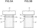
- FIGS. 5A and 5B are explanatory drawings showing positions and shapes of coating parts 51 and 55 in flexible printed circuit boards 31 and 35.
- FIG. 5A is a diagram showing the coating part 51 of a first embodiment.
- FIG. 5B is a diagram showing the coating part 55 of a second embodiment.
- the notch part 47a is formed in such a way that the insulative coat 47 is peeled (stripped) off into a strip shape in the width direction across the whole width of the flexible printed circuit board 31. Thereby, the notch part 47a is formed along the direction of the gap 41 (see FIG. 4 ) extending, and the area of the exposed part 44A (see FIG. 4 ) (or coating part 51) is large. Hence, static electricity can be more easily guided.
- the notch part 47b of the insulative coat 47 is formed into an oval shape extending in the width direction of the flexible printed circuit board 31.
- the coating part 55 constituted by plating is provided so as to cover the entirety of an exposed part (not shown) formed with the notch part 47b on the conductor part 44.
- the shapes of the notch parts 47a and 47b are not limited to the aforementioned shapes but may be circular, ellipsoidal, rectangular or in another shape. The point is that the conductor part 44 (or coating parts 51 and 55) is externally exposed and can take in static electricity.
- the flexible printed circuit board 31 connected to the control printed circuit board 26 as a circuit board contained in the front casing 22 of the display device 12 is provided.
- the flexible printed circuit board 31 has two layers of the conductor parts 43 and 44, the surfaces of these conductor parts 43 and 44 are covered with the insulative coats 46 and 47, the exposed part 44A (or coating part 51 as the exposed part) through which the conductor part 44 is externally exposed by peeling off the insulative coat 47 at a portion opposing the gap 41 is formed, and the conductor part 44 having this exposed part 44A is grounded.
- the exposed part 44A (or coating part 51) is provided at a position closer to the gap 41 than the bonding part, to the touch panel 27, which is provided to the end part of the flexible printed circuit board 31 or the similar part, by providing the exposed part 44A (or coating part 51) at a position closer to the gap 41, static electricity can easily reach the exposed part 44A (coating part 51) from the gap 41, and electrostatic surge can be prevented from occurring.
- the plating can prevent corrosion of the exposed part 44A of the conductor part 44, and electrostatic surge can be prevented from occurring for a long time.
- the two members are constituted of the front casing 22 constituting the front part of the in-vehicle electronic device and the touch panel 27 (or touch panel assembly 21) attached to this front casing 22, and the flexible printed circuit board 31 connects the touch panel 27 to the touch panel control circuit provided on the control printed circuit board 26, electrostatic surge due to static electricity flowing from an occupant operating the touch panel 27 can be prevented from occurring, and damage to an IC or the like of the touch panel control circuit can be prevented.
Landscapes
- Engineering & Computer Science (AREA)
- Mechanical Engineering (AREA)
- Chemical & Material Sciences (AREA)
- Combustion & Propulsion (AREA)
- Transportation (AREA)
- Microelectronics & Electronic Packaging (AREA)
- Elimination Of Static Electricity (AREA)
- Switches That Are Operated By Magnetic Or Electric Fields (AREA)
- Shielding Devices Or Components To Electric Or Magnetic Fields (AREA)
Claims (4)
- Structure de prévention de surtension électrostatique, dans laquelle
une carte de circuit imprimé flexible (31) connectée à une carte de circuit (26) contenue dans un dispositif électronique (10) est prévue à une position correspondant à un écartement (41), entre deux organes, apparaissant dans le dispositif électronique (10), les deux organes sont constitués d'un boîtier avant (22) et d'un dispositif d'affichage (12), ou du boîtier avant (22) et d'un panneau tactile (27),
caractérisée en ce que la carte de circuit imprimé flexible (31) possède deux couches de parties de conducteur (43, 44), des surfaces de ces parties de conducteur (43, 44) sont couvertes avec des revêtements isolants (46, 47), une partie exposée (44A) à travers laquelle l'une des parties de conducteur (43, 44) est exposée de manière externe est formée au niveau d'une portion opposée à l'écartement (41) par décollement du revêtement isolant (47), et la partie de conducteur (44) ayant la partie exposée (44A) est mise à la terre,
la partie exposée (44A) est formée de telle sorte que le revêtement isolant (47) soit décollé dans une forme de bande dans la direction de la largeur sur toute la largeur de la carte de circuit imprimé flexible (31). - Structure de prévention de surtension électrostatique selon la revendication 1, dans laquelle la partie exposée (44A) est prévue à une position plus proche de l'écartement (41) qu'une partie de connexion prévue dans une partie d'extrémité de la carte de circuit imprimé flexible (31).
- Structure de prévention de surtension électrostatique selon la revendication 1 ou 2, dans laquelle la partie exposée (44A) subit un placage avec conductivité.
- Structure de prévention de surtension électrostatique selon l'une quelconque des revendications 1 à 3, dans laquelle
les deux organes sont constitués d'un boîtier avant (22) constituant une partie avant du dispositif électronique (10) à mettre en œuvre dans un véhicule, et le panneau tactile (27) attaché au boîtier avant (22), et
la carte de circuit imprimé flexible (31) connecte le panneau tactile (27) à un circuit de commande de panneau tactile prévu dans la carte de circuit (26).
Applications Claiming Priority (2)
| Application Number | Priority Date | Filing Date | Title |
|---|---|---|---|
| JP2014148466A JP6396707B2 (ja) | 2014-07-22 | 2014-07-22 | 静電サージ防止構造 |
| PCT/JP2015/065373 WO2016013292A1 (fr) | 2014-07-22 | 2015-05-28 | Structure de prévention de pic électrostatique |
Publications (3)
| Publication Number | Publication Date |
|---|---|
| EP3174372A1 EP3174372A1 (fr) | 2017-05-31 |
| EP3174372A4 EP3174372A4 (fr) | 2018-04-11 |
| EP3174372B1 true EP3174372B1 (fr) | 2020-08-05 |
Family
ID=55162828
Family Applications (1)
| Application Number | Title | Priority Date | Filing Date |
|---|---|---|---|
| EP15823941.8A Not-in-force EP3174372B1 (fr) | 2014-07-22 | 2015-05-28 | Structure de prévention de pic électrostatique |
Country Status (5)
| Country | Link |
|---|---|
| US (1) | US10559955B2 (fr) |
| EP (1) | EP3174372B1 (fr) |
| JP (1) | JP6396707B2 (fr) |
| CN (1) | CN106664786B (fr) |
| WO (1) | WO2016013292A1 (fr) |
Families Citing this family (4)
| Publication number | Priority date | Publication date | Assignee | Title |
|---|---|---|---|---|
| JP6455154B2 (ja) * | 2015-01-08 | 2019-01-23 | 株式会社デンソー | 車両用電子機器 |
| DE102015016281A1 (de) * | 2015-12-16 | 2017-06-22 | GM Global Technology Operations LLC (n. d. Ges. d. Staates Delaware) | Windschutzscheibe eines Kraftfahrzeugs, System mit Windschutzscheibe sowie Kraftfahrzeug |
| CN108566189A (zh) * | 2018-05-03 | 2018-09-21 | 王汉禄 | 触摸固态开关 |
| CN116600456B (zh) * | 2023-07-18 | 2023-09-08 | 深圳市凯泰精密设备有限公司 | 一种大数据服务器机箱静电防护装置 |
Family Cites Families (11)
| Publication number | Priority date | Publication date | Assignee | Title |
|---|---|---|---|---|
| JP2001043022A (ja) * | 1999-07-30 | 2001-02-16 | Matsushita Electric Ind Co Ltd | 透明タッチパネルおよびこれを用いた電子機器 |
| JP4055672B2 (ja) | 2003-07-31 | 2008-03-05 | 株式会社デンソー | 表示装置 |
| CN2648764Y (zh) | 2003-08-18 | 2004-10-13 | 仁宝电脑工业股份有限公司 | 静电消除装置 |
| JP5026163B2 (ja) * | 2007-06-26 | 2012-09-12 | セイコーインスツル株式会社 | 電子機器 |
| JP2009158808A (ja) * | 2007-12-27 | 2009-07-16 | Kyocera Corp | フレキシブル基板及びこれを用いた携帯電子機器 |
| CN201788332U (zh) | 2010-08-09 | 2011-04-06 | 东莞通华液晶有限公司 | 可加速静电消散的防静电液晶显示屏 |
| CN202121863U (zh) | 2011-06-16 | 2012-01-18 | 湖北奕宏精密制造有限公司 | 一种抗干扰的柔性电路板 |
| JP6338348B2 (ja) | 2012-12-26 | 2018-06-06 | キヤノン株式会社 | フレキシブルプリント基板及び電子機器 |
| KR102042678B1 (ko) * | 2013-03-25 | 2019-11-11 | 삼성디스플레이 주식회사 | 디스플레이 장치 |
| CN103594022A (zh) | 2013-11-21 | 2014-02-19 | 友达光电(厦门)有限公司 | 显示装置 |
| TWI494822B (zh) * | 2013-12-06 | 2015-08-01 | Au Optronics Corp | 具可撓性電路模組之觸控顯示裝置 |
-
2014
- 2014-07-22 JP JP2014148466A patent/JP6396707B2/ja active Active
-
2015
- 2015-05-28 WO PCT/JP2015/065373 patent/WO2016013292A1/fr not_active Ceased
- 2015-05-28 EP EP15823941.8A patent/EP3174372B1/fr not_active Not-in-force
- 2015-05-28 CN CN201580035099.1A patent/CN106664786B/zh active Active
- 2015-05-28 US US15/317,254 patent/US10559955B2/en active Active
Non-Patent Citations (1)
| Title |
|---|
| None * |
Also Published As
| Publication number | Publication date |
|---|---|
| US20170141566A1 (en) | 2017-05-18 |
| EP3174372A1 (fr) | 2017-05-31 |
| CN106664786B (zh) | 2018-05-04 |
| CN106664786A (zh) | 2017-05-10 |
| JP6396707B2 (ja) | 2018-09-26 |
| EP3174372A4 (fr) | 2018-04-11 |
| US10559955B2 (en) | 2020-02-11 |
| JP2016024961A (ja) | 2016-02-08 |
| WO2016013292A1 (fr) | 2016-01-28 |
Similar Documents
| Publication | Publication Date | Title |
|---|---|---|
| US20130194759A1 (en) | Touch sensor with integrated signal bus extensions | |
| EP3174372B1 (fr) | Structure de prévention de pic électrostatique | |
| JP2013246626A (ja) | タッチパネル及びこれを用いた入力装置 | |
| JP7233037B2 (ja) | タッチセンサおよびそれを用いた表示装置 | |
| KR20150103612A (ko) | 디지타이저 | |
| US10847908B2 (en) | Connected board and display device | |
| JP2024033004A (ja) | センサ及びその製造方法 | |
| US20140027263A1 (en) | Touch panel and method for manufacturing same | |
| KR20180120760A (ko) | 정전 용량식 센서 | |
| JP5814837B2 (ja) | 意匠板およびタッチパネル入力表示機器 | |
| JP2013097457A (ja) | センサーシート | |
| EP3232302B1 (fr) | Écran tactile | |
| JP6529866B2 (ja) | 静電容量式センサ、タッチパネルおよび電子機器 | |
| JP2019175064A (ja) | タッチパネル装置、およびフレキシブル基板 | |
| JP2015069609A (ja) | タッチパネル | |
| KR101154553B1 (ko) | 터치입력장치 | |
| JP7205860B2 (ja) | 静電方式の入力装置 | |
| TWI581146B (zh) | 觸控面板 | |
| WO2014196173A1 (fr) | Dispositif d'affichage | |
| CN211349320U (zh) | 一种具有触摸屏的电子设备 | |
| CN210573698U (zh) | 一种具有触摸屏的电子设备 | |
| WO2017154617A1 (fr) | Capteur de capacité électrostatique | |
| WO2022014161A1 (fr) | Capteur tactile et dispositif à écran tactile | |
| KR20100054898A (ko) | 터치입력장치 | |
| JP2021071846A (ja) | タッチセンサ |
Legal Events
| Date | Code | Title | Description |
|---|---|---|---|
| STAA | Information on the status of an ep patent application or granted ep patent |
Free format text: STATUS: THE INTERNATIONAL PUBLICATION HAS BEEN MADE |
|
| PUAI | Public reference made under article 153(3) epc to a published international application that has entered the european phase |
Free format text: ORIGINAL CODE: 0009012 |
|
| STAA | Information on the status of an ep patent application or granted ep patent |
Free format text: STATUS: REQUEST FOR EXAMINATION WAS MADE |
|
| 17P | Request for examination filed |
Effective date: 20170221 |
|
| AK | Designated contracting states |
Kind code of ref document: A1 Designated state(s): AL AT BE BG CH CY CZ DE DK EE ES FI FR GB GR HR HU IE IS IT LI LT LU LV MC MK MT NL NO PL PT RO RS SE SI SK SM TR |
|
| AX | Request for extension of the european patent |
Extension state: BA ME |
|
| DAV | Request for validation of the european patent (deleted) | ||
| DAX | Request for extension of the european patent (deleted) | ||
| A4 | Supplementary search report drawn up and despatched |
Effective date: 20180313 |
|
| RIC1 | Information provided on ipc code assigned before grant |
Ipc: H05F 3/02 20060101AFI20180306BHEP Ipc: B60R 16/02 20060101ALI20180306BHEP Ipc: H05K 9/00 20060101ALI20180306BHEP |
|
| GRAP | Despatch of communication of intention to grant a patent |
Free format text: ORIGINAL CODE: EPIDOSNIGR1 |
|
| STAA | Information on the status of an ep patent application or granted ep patent |
Free format text: STATUS: GRANT OF PATENT IS INTENDED |
|
| INTG | Intention to grant announced |
Effective date: 20200319 |
|
| GRAS | Grant fee paid |
Free format text: ORIGINAL CODE: EPIDOSNIGR3 |
|
| GRAA | (expected) grant |
Free format text: ORIGINAL CODE: 0009210 |
|
| STAA | Information on the status of an ep patent application or granted ep patent |
Free format text: STATUS: THE PATENT HAS BEEN GRANTED |
|
| AK | Designated contracting states |
Kind code of ref document: B1 Designated state(s): AL AT BE BG CH CY CZ DE DK EE ES FI FR GB GR HR HU IE IS IT LI LT LU LV MC MK MT NL NO PL PT RO RS SE SI SK SM TR |
|
| REG | Reference to a national code |
Ref country code: GB Ref legal event code: FG4D |
|
| REG | Reference to a national code |
Ref country code: CH Ref legal event code: EP |
|
| REG | Reference to a national code |
Ref country code: AT Ref legal event code: REF Ref document number: 1300570 Country of ref document: AT Kind code of ref document: T Effective date: 20200815 |
|
| REG | Reference to a national code |
Ref country code: DE Ref legal event code: R096 Ref document number: 602015057089 Country of ref document: DE |
|
| REG | Reference to a national code |
Ref country code: IE Ref legal event code: FG4D |
|
| REG | Reference to a national code |
Ref country code: LT Ref legal event code: MG4D |
|
| REG | Reference to a national code |
Ref country code: NL Ref legal event code: MP Effective date: 20200805 |
|
| REG | Reference to a national code |
Ref country code: AT Ref legal event code: MK05 Ref document number: 1300570 Country of ref document: AT Kind code of ref document: T Effective date: 20200805 |
|
| PG25 | Lapsed in a contracting state [announced via postgrant information from national office to epo] |
Ref country code: PT Free format text: LAPSE BECAUSE OF FAILURE TO SUBMIT A TRANSLATION OF THE DESCRIPTION OR TO PAY THE FEE WITHIN THE PRESCRIBED TIME-LIMIT Effective date: 20201207 Ref country code: GR Free format text: LAPSE BECAUSE OF FAILURE TO SUBMIT A TRANSLATION OF THE DESCRIPTION OR TO PAY THE FEE WITHIN THE PRESCRIBED TIME-LIMIT Effective date: 20201106 Ref country code: ES Free format text: LAPSE BECAUSE OF FAILURE TO SUBMIT A TRANSLATION OF THE DESCRIPTION OR TO PAY THE FEE WITHIN THE PRESCRIBED TIME-LIMIT Effective date: 20200805 Ref country code: AT Free format text: LAPSE BECAUSE OF FAILURE TO SUBMIT A TRANSLATION OF THE DESCRIPTION OR TO PAY THE FEE WITHIN THE PRESCRIBED TIME-LIMIT Effective date: 20200805 Ref country code: BG Free format text: LAPSE BECAUSE OF FAILURE TO SUBMIT A TRANSLATION OF THE DESCRIPTION OR TO PAY THE FEE WITHIN THE PRESCRIBED TIME-LIMIT Effective date: 20201105 Ref country code: NO Free format text: LAPSE BECAUSE OF FAILURE TO SUBMIT A TRANSLATION OF THE DESCRIPTION OR TO PAY THE FEE WITHIN THE PRESCRIBED TIME-LIMIT Effective date: 20201105 Ref country code: LT Free format text: LAPSE BECAUSE OF FAILURE TO SUBMIT A TRANSLATION OF THE DESCRIPTION OR TO PAY THE FEE WITHIN THE PRESCRIBED TIME-LIMIT Effective date: 20200805 Ref country code: FI Free format text: LAPSE BECAUSE OF FAILURE TO SUBMIT A TRANSLATION OF THE DESCRIPTION OR TO PAY THE FEE WITHIN THE PRESCRIBED TIME-LIMIT Effective date: 20200805 Ref country code: SE Free format text: LAPSE BECAUSE OF FAILURE TO SUBMIT A TRANSLATION OF THE DESCRIPTION OR TO PAY THE FEE WITHIN THE PRESCRIBED TIME-LIMIT Effective date: 20200805 Ref country code: HR Free format text: LAPSE BECAUSE OF FAILURE TO SUBMIT A TRANSLATION OF THE DESCRIPTION OR TO PAY THE FEE WITHIN THE PRESCRIBED TIME-LIMIT Effective date: 20200805 |
|
| PG25 | Lapsed in a contracting state [announced via postgrant information from national office to epo] |
Ref country code: LV Free format text: LAPSE BECAUSE OF FAILURE TO SUBMIT A TRANSLATION OF THE DESCRIPTION OR TO PAY THE FEE WITHIN THE PRESCRIBED TIME-LIMIT Effective date: 20200805 Ref country code: PL Free format text: LAPSE BECAUSE OF FAILURE TO SUBMIT A TRANSLATION OF THE DESCRIPTION OR TO PAY THE FEE WITHIN THE PRESCRIBED TIME-LIMIT Effective date: 20200805 Ref country code: RS Free format text: LAPSE BECAUSE OF FAILURE TO SUBMIT A TRANSLATION OF THE DESCRIPTION OR TO PAY THE FEE WITHIN THE PRESCRIBED TIME-LIMIT Effective date: 20200805 Ref country code: NL Free format text: LAPSE BECAUSE OF FAILURE TO SUBMIT A TRANSLATION OF THE DESCRIPTION OR TO PAY THE FEE WITHIN THE PRESCRIBED TIME-LIMIT Effective date: 20200805 Ref country code: IS Free format text: LAPSE BECAUSE OF FAILURE TO SUBMIT A TRANSLATION OF THE DESCRIPTION OR TO PAY THE FEE WITHIN THE PRESCRIBED TIME-LIMIT Effective date: 20201205 |
|
| PG25 | Lapsed in a contracting state [announced via postgrant information from national office to epo] |
Ref country code: CZ Free format text: LAPSE BECAUSE OF FAILURE TO SUBMIT A TRANSLATION OF THE DESCRIPTION OR TO PAY THE FEE WITHIN THE PRESCRIBED TIME-LIMIT Effective date: 20200805 Ref country code: DK Free format text: LAPSE BECAUSE OF FAILURE TO SUBMIT A TRANSLATION OF THE DESCRIPTION OR TO PAY THE FEE WITHIN THE PRESCRIBED TIME-LIMIT Effective date: 20200805 Ref country code: EE Free format text: LAPSE BECAUSE OF FAILURE TO SUBMIT A TRANSLATION OF THE DESCRIPTION OR TO PAY THE FEE WITHIN THE PRESCRIBED TIME-LIMIT Effective date: 20200805 Ref country code: RO Free format text: LAPSE BECAUSE OF FAILURE TO SUBMIT A TRANSLATION OF THE DESCRIPTION OR TO PAY THE FEE WITHIN THE PRESCRIBED TIME-LIMIT Effective date: 20200805 Ref country code: SM Free format text: LAPSE BECAUSE OF FAILURE TO SUBMIT A TRANSLATION OF THE DESCRIPTION OR TO PAY THE FEE WITHIN THE PRESCRIBED TIME-LIMIT Effective date: 20200805 |
|
| REG | Reference to a national code |
Ref country code: DE Ref legal event code: R097 Ref document number: 602015057089 Country of ref document: DE |
|
| PG25 | Lapsed in a contracting state [announced via postgrant information from national office to epo] |
Ref country code: AL Free format text: LAPSE BECAUSE OF FAILURE TO SUBMIT A TRANSLATION OF THE DESCRIPTION OR TO PAY THE FEE WITHIN THE PRESCRIBED TIME-LIMIT Effective date: 20200805 |
|
| PLBE | No opposition filed within time limit |
Free format text: ORIGINAL CODE: 0009261 |
|
| STAA | Information on the status of an ep patent application or granted ep patent |
Free format text: STATUS: NO OPPOSITION FILED WITHIN TIME LIMIT |
|
| PG25 | Lapsed in a contracting state [announced via postgrant information from national office to epo] |
Ref country code: SK Free format text: LAPSE BECAUSE OF FAILURE TO SUBMIT A TRANSLATION OF THE DESCRIPTION OR TO PAY THE FEE WITHIN THE PRESCRIBED TIME-LIMIT Effective date: 20200805 |
|
| 26N | No opposition filed |
Effective date: 20210507 |
|
| PG25 | Lapsed in a contracting state [announced via postgrant information from national office to epo] |
Ref country code: IT Free format text: LAPSE BECAUSE OF FAILURE TO SUBMIT A TRANSLATION OF THE DESCRIPTION OR TO PAY THE FEE WITHIN THE PRESCRIBED TIME-LIMIT Effective date: 20200805 |
|
| PG25 | Lapsed in a contracting state [announced via postgrant information from national office to epo] |
Ref country code: SI Free format text: LAPSE BECAUSE OF FAILURE TO SUBMIT A TRANSLATION OF THE DESCRIPTION OR TO PAY THE FEE WITHIN THE PRESCRIBED TIME-LIMIT Effective date: 20200805 |
|
| PGFP | Annual fee paid to national office [announced via postgrant information from national office to epo] |
Ref country code: GB Payment date: 20210422 Year of fee payment: 7 |
|
| REG | Reference to a national code |
Ref country code: CH Ref legal event code: PL |
|
| PG25 | Lapsed in a contracting state [announced via postgrant information from national office to epo] |
Ref country code: LI Free format text: LAPSE BECAUSE OF NON-PAYMENT OF DUE FEES Effective date: 20210531 Ref country code: LU Free format text: LAPSE BECAUSE OF NON-PAYMENT OF DUE FEES Effective date: 20210528 Ref country code: MC Free format text: LAPSE BECAUSE OF FAILURE TO SUBMIT A TRANSLATION OF THE DESCRIPTION OR TO PAY THE FEE WITHIN THE PRESCRIBED TIME-LIMIT Effective date: 20200805 Ref country code: CH Free format text: LAPSE BECAUSE OF NON-PAYMENT OF DUE FEES Effective date: 20210531 |
|
| REG | Reference to a national code |
Ref country code: BE Ref legal event code: MM Effective date: 20210531 |
|
| PG25 | Lapsed in a contracting state [announced via postgrant information from national office to epo] |
Ref country code: IE Free format text: LAPSE BECAUSE OF NON-PAYMENT OF DUE FEES Effective date: 20210528 |
|
| PG25 | Lapsed in a contracting state [announced via postgrant information from national office to epo] |
Ref country code: BE Free format text: LAPSE BECAUSE OF NON-PAYMENT OF DUE FEES Effective date: 20210531 |
|
| GBPC | Gb: european patent ceased through non-payment of renewal fee |
Effective date: 20220528 |
|
| PG25 | Lapsed in a contracting state [announced via postgrant information from national office to epo] |
Ref country code: HU Free format text: LAPSE BECAUSE OF FAILURE TO SUBMIT A TRANSLATION OF THE DESCRIPTION OR TO PAY THE FEE WITHIN THE PRESCRIBED TIME-LIMIT; INVALID AB INITIO Effective date: 20150528 Ref country code: GB Free format text: LAPSE BECAUSE OF NON-PAYMENT OF DUE FEES Effective date: 20220528 |
|
| PG25 | Lapsed in a contracting state [announced via postgrant information from national office to epo] |
Ref country code: CY Free format text: LAPSE BECAUSE OF FAILURE TO SUBMIT A TRANSLATION OF THE DESCRIPTION OR TO PAY THE FEE WITHIN THE PRESCRIBED TIME-LIMIT Effective date: 20200805 |
|
| REG | Reference to a national code |
Ref country code: DE Ref legal event code: R082 Ref document number: 602015057089 Country of ref document: DE Representative=s name: GLAWE DELFS MOLL PARTNERSCHAFT MBB VON PATENT-, DE Ref country code: DE Ref legal event code: R082 Ref document number: 602015057089 Country of ref document: DE Representative=s name: GLAWE DELFS MOLL PARTGMBB, DE |
|
| PG25 | Lapsed in a contracting state [announced via postgrant information from national office to epo] |
Ref country code: MK Free format text: LAPSE BECAUSE OF FAILURE TO SUBMIT A TRANSLATION OF THE DESCRIPTION OR TO PAY THE FEE WITHIN THE PRESCRIBED TIME-LIMIT Effective date: 20200805 |
|
| PGFP | Annual fee paid to national office [announced via postgrant information from national office to epo] |
Ref country code: DE Payment date: 20240418 Year of fee payment: 10 |
|
| PGFP | Annual fee paid to national office [announced via postgrant information from national office to epo] |
Ref country code: FR Payment date: 20240418 Year of fee payment: 10 |
|
| PG25 | Lapsed in a contracting state [announced via postgrant information from national office to epo] |
Ref country code: MT Free format text: LAPSE BECAUSE OF FAILURE TO SUBMIT A TRANSLATION OF THE DESCRIPTION OR TO PAY THE FEE WITHIN THE PRESCRIBED TIME-LIMIT Effective date: 20200805 |
|
| REG | Reference to a national code |
Ref country code: DE Ref legal event code: R119 Ref document number: 602015057089 Country of ref document: DE |
|
| PG25 | Lapsed in a contracting state [announced via postgrant information from national office to epo] |
Ref country code: TR Free format text: LAPSE BECAUSE OF FAILURE TO SUBMIT A TRANSLATION OF THE DESCRIPTION OR TO PAY THE FEE WITHIN THE PRESCRIBED TIME-LIMIT Effective date: 20200805 |
|
| PG25 | Lapsed in a contracting state [announced via postgrant information from national office to epo] |
Ref country code: DE Free format text: LAPSE BECAUSE OF NON-PAYMENT OF DUE FEES Effective date: 20251202 |
|
| PG25 | Lapsed in a contracting state [announced via postgrant information from national office to epo] |
Ref country code: FR Free format text: LAPSE BECAUSE OF NON-PAYMENT OF DUE FEES Effective date: 20250531 |