EP3182248B1 - Leistungsbereichsstromverteilung - Google Patents
Leistungsbereichsstromverteilung Download PDFInfo
- Publication number
- EP3182248B1 EP3182248B1 EP16204335.0A EP16204335A EP3182248B1 EP 3182248 B1 EP3182248 B1 EP 3182248B1 EP 16204335 A EP16204335 A EP 16204335A EP 3182248 B1 EP3182248 B1 EP 3182248B1
- Authority
- EP
- European Patent Office
- Prior art keywords
- power
- domain
- current
- voltage
- signal
- Prior art date
- Legal status (The legal status is an assumption and is not a legal conclusion. Google has not performed a legal analysis and makes no representation as to the accuracy of the status listed.)
- Not-in-force
Links
Images


Classifications
-
- G—PHYSICS
- G05—CONTROLLING; REGULATING
- G05F—SYSTEMS FOR REGULATING ELECTRIC OR MAGNETIC VARIABLES
- G05F1/00—Automatic systems in which deviations of an electric quantity from one or more predetermined values are detected at the output of the system and fed back to a device within the system to restore the detected quantity to its predetermined value or values, i.e. retroactive systems
- G05F1/66—Regulating electric power
-
- H—ELECTRICITY
- H02—GENERATION; CONVERSION OR DISTRIBUTION OF ELECTRIC POWER
- H02J—ELECTRIC POWER NETWORKS; CIRCUIT ARRANGEMENTS OR SYSTEMS FOR SUPPLYING OR DISTRIBUTING ELECTRIC POWER; SYSTEMS FOR STORING ELECTRIC ENERGY
- H02J3/00—Circuit arrangements for AC mains or AC distribution networks
- H02J3/12—Arrangements for adjusting voltage in AC networks by changing a characteristic of the network load
-
- G—PHYSICS
- G05—CONTROLLING; REGULATING
- G05B—CONTROL OR REGULATING SYSTEMS IN GENERAL; FUNCTIONAL ELEMENTS OF SUCH SYSTEMS; MONITORING OR TESTING ARRANGEMENTS FOR SUCH SYSTEMS OR ELEMENTS
- G05B15/00—Systems controlled by a computer
- G05B15/02—Systems controlled by a computer electric
-
- G—PHYSICS
- G06—COMPUTING OR CALCULATING; COUNTING
- G06F—ELECTRIC DIGITAL DATA PROCESSING
- G06F1/00—Details not covered by groups G06F3/00 - G06F13/00 and G06F21/00
- G06F1/26—Power supply means, e.g. regulation thereof
- G06F1/32—Means for saving power
- G06F1/3203—Power management, i.e. event-based initiation of a power-saving mode
- G06F1/3206—Monitoring of events, devices or parameters that trigger a change in power modality
Definitions
- the present specification relates to systems, methods, apparatuses, devices, articles of manufacture and instructions for power management.
- Energy minimization using charge recycling can be used for such power sensitive systems. Energy/charge recycling is applied to circuits or systems having two or more power-domains.
- Energy/charge recycling are techniques for optimizing energy efficiency of a set of power-domains (e.g. circuits and/or computing platforms). Such techniques can be based on using circuit stacking (e.g. memory on top of logic) for recycling a charge, resulting in static and/or dynamic power reductions. Such techniques reduce voltage regulation power losses.
- An apparatus for power management comprises a current sink/source sensor configured to monitor a power-supply to inter-power-domain sink/source-current and to generate a current mismatch signal if the power-supply to inter-power-domain sink/source-current exceeds a threshold range; and a current imbalance controller coupled to receive the current mismatch signal and configured to generate a set of power-domain control signals; wherein the set of power-domain control signals reduce an absolute value of the power-supply to inter-power-domain sink/source-current.
- the threshold range includes zero Amps.
- the power-supply to inter-power-domain sink/source-current is a current either supplied to or sunk from an electrical node in between a top power-domain and a bottom power-domain.
- top and bottom power-domains are in a stacked configuration employing charge recycling.
- the top and bottom power-domains are matched circuits.
- one of the power-domains is a memory circuit and another is a computational logic circuit.
- the set of power-domain control signals include at least one of: a voltage control signal, a frequency control signal, and a task control signal.
- a power-domain voltage controller coupled to the current imbalance controller; wherein the voltage controller adds a top power-domain voltage selection signal and a bottom power-domain voltage selection signal to the set of power-domain control signals; and wherein the voltage selection signals are configured to reduce the absolute value of the power-supply to inter-power-domain sink/source-current.
- the top power-domain voltage selection signal selects a reduced top power-domain voltage if the current mismatch signal indicates that a top power-domain current is greater than a bottom power-domain current.
- the bottom power-domain voltage selection signal selects an increased bottom power-domain voltage if the current mismatch signal indicates that a top power-domain current is greater than a bottom power-domain current.
- a power-domain frequency controller coupled to the current imbalance controller; wherein the frequency controller adds a top power-domain frequency selection signal and a bottom power-domain frequency selection signal to the set of power-domain control signals; and wherein the frequency selection signals are configured to reduce the absolute value of the power-supply to inter-power-domain sink/source-current.
- the top power-domain frequency selection signal selects a reduced top power-domain frequency if the current mismatch signal indicates that a top power-domain current is greater than a bottom power-domain current.
- a power-domain task controller coupled to the current imbalance controller; wherein the task controller adds a top power-domain task selection signal and a bottom power-domain task selection signal to the set of power-domain control signals; and wherein the task selection signals are configured to reduce the absolute value of the power-supply to inter-power-domain sink/source-current.
- the top power-domain task selection signal selects a reduced load of top power-domain tasks.
- the task selection signal includes at least one of: a logic selection signal, a firmware selection signal or software execute signal.
- the task selection signal instructs a portion of at least one of the power-domains to turn on or off.
- the task selection signal instructs a portion of at least one of the power-domains to executed a set of software instructions or not.
- the current imbalance controller is an adaptive relative voltage and frequency scaling (ARVFS) controller.
- ARVFS adaptive relative voltage and frequency scaling
- an article of manufacture including at least one non-transitory, tangible machine readable storage medium containing executable machine instructions for power management, wherein the instructions comprise: monitoring a power-supply to inter-power-domain sink/source-current; generating a current mismatch signal if the power-supply to inter-power-domain sink/source-current exceeds a threshold range; and generating a set of power-domain control signals in response to the current mismatch signal so as to reduce an absolute value of the power-supply to inter-power-domain sink/source-current.
- the set of power-domain control signals include at least one of: a voltage control signal, a frequency control signal, a task control signal and a substrate bias control signal.
- Circuit partitioning has a direct effect on how well energy/charge recycling and load-balancing (i.e. minimizing the current variations) can be optimized between two or more power-domains.
- a circuit is partitioned into two or more almost equal current consuming blocks (i.e. symmetric/mirrored circuit partitioning). For example, in a dual-CPU system where, one CPU is in the top power-domain and second CPU is in the bottom power-domain.
- other functionalities like memory (SRAM) may also be equally split between two or more power-domains.
- SRAM static random access memory
- I-top i.e. current for the top power-domain
- I-bottom i.e. current for the bottom power-domain
- symmetric/mirrored functionalities may either not be possible or preferable.
- a CPU in a top-power-domain may require a first voltage and frequency
- a memory in the bottom-power-domain may require a second different voltage and frequency.
- These different functionalities can also have unequal current requirements.
- memory consumes 20-40% less power than the logic in an MCU or CPU.
- circuits and techniques better align current consumption and thus load-balancing between a set of power-domains.
- FIG. 1 is one example of an apparatus 100 for power-domain current balance.
- the apparatus 100 includes a top power-domain 102 energized by a top voltage (VDD-top) 104 and a top current (I-top) 106, a bottom power-domain 108 energized by a bottom voltage (VDD-bottom) 110 and a bottom current (I- bottom) 112, a current sink/source sensor 114 outputting a current mismatch signal (I-mismatch/I-imbalance signal) 116.
- Signal level-shifters (not shown) between the top and bottom power-domains 102, 108 enable a first set of analog and/or digital voltage signal ranges defined for the top power-domain 102 to be translated into a second set of analog and/or digital voltage signal ranges defined for the bottom power-domain 108 thereby enabling proper communication between these power-domains 102, 108.
- the top and bottom power-domains 102, 108 attributes vary depending upon their application.
- the power-domains 102, 108 could be matched circuits, or one could be a memory circuit and the other a computational logic circuit (e.g. memory on top of logic MOTL configuration).
- the top and bottom power-domains 102, 108 can have different power consumption profiles based on their operational tasks (e.g. logic, firmware and/or software functionalities), operating voltages and/or operating frequencies.
- the task load can be varied by either turning on or off circuits in one or more of the power-domain's 102, 108 or by reapportioning the software executed by each of the power-domains 102, 108.
- a power supply 118 supplies the voltage and current to the top and bottom power-domains 102, 108.
- a current imbalance controller 124 receives the current mismatch signal (I-mismatch signal) 116 and reduces any current imbalances between the top and bottom power-domains 102, 108.
- the current imbalance controller 124 reduces the current imbalances between the top and bottom power-domains 102, 108 using a voltage controller 126, a frequency controller 128, a task controller 130 and/or a substrate bias controller 132. These controllers ensure an embedded close-loop control loop architecture and provides negative feedback to compensate for the imbalance.
- the current sink/source sensor 114 is configured to monitor a power-supply to inter-power-domain sink/source-current (i.e. the sink/source current 122).
- the power-supply to inter-power-domain sink/source-current is a current either supplied to or sunk from an electrical node in between a top power-domain and a bottom power-domain as shown in Figure 1 .
- This electrical node in one example can also be used to monitor the bottom voltage (VDD-bottom) 110 or the top voltage (VDD-top) 104, depending upon the current sink/source sensor's 114 configuration.
- the current sink/source sensor 114 generates the current mismatch signal 116 if the power-supply to inter-power-domain sink/source-current 122 exceeds a threshold range.
- An example threshold range could be +/- 1 ⁇ A centered about 0 Amps, or may be offset and centered about a non-zero current or voltage level. For this, there is hysteresis built in to provide stability in the loop control.
- the current imbalance controller 124 receives and monitors the current mismatch signal 116, which in various embodiments may also include receiving and monitoring the threshold range.
- the current imbalance controller 124 generates a set of power-domain control signals which are sent to one or more of the power-domains 102, 108 to reduce an absolute value of the power-supply to inter-power-domain sink/source-current.
- the power-domain current imbalance controller 124 contains logic, firmware and/or software configured to use adaptive relative voltage and frequency scaling (ARVFS) techniques to reduce any current mismatch.
- ARVFS adaptive relative voltage and frequency scaling
- the ARVFS techniques monitor an amount of current mismatch between the power-domains (e.g. the stacked elements) and adjusts voltage, frequency and task assignments (e.g. logic, firmware and/or software functionalities) as control elements to compensate for any load-imbalance.
- the instructions are part of an embedded control loop.
- the current imbalance controller 124 is constrained in an ability to vary the voltage, frequency and task assignments due to the physical design of the power-domains 102, 108 (i.e. maximum and minimum operating voltages and frequencies, as well as ability to execute certain tasks).
- constraints include: Minimum throughput of individual power-domains or combined total throughput of two power-domains; Voltage headroom for individual power-domains and/or the total headroom for two power-domains (i.e. V-top + V-bottom); and Allowed frequency Vs Voltage of each power-domain, (i.e. interdependency of voltage and frequency).
- the voltage controller 126 adds a top power-domain voltage selection signal and a bottom power-domain voltage selection signal to the set of power-domain control signals. These voltage selection signals are configured to reduce the absolute value of the power-supply to inter-power-domain sink/source-current.
- the top power-domain voltage selection signal can select a reduced top power-domain voltage, or the bottom power-domain voltage selection signal can select an increased bottom power-domain voltage.
- the frequency controller 128 adds a top power-domain frequency selection signal and a bottom power-domain frequency selection signal to the set of power-domain control signals. These frequency selection signals can also be configured to reduce the absolute value of the power-supply to inter-power-domain sink/source-current.
- the top power-domain frequency selection signal can select a reduced top power-domain frequency.
- the task controller 130 adds a top power-domain task selection signal and a bottom power-domain task selection signal to the set of power-domain control signals. These task selection signals can similarly be configured to reduce the absolute value of the power-supply to inter-power-domain sink/source-current.
- the top power-domain task selection signal can select a reduced load of top power-domain tasks.
- the task selection signal includes at least one of: a logic selection signal, a firmware selection signal or software execute signal.
- the task selection signal can instruct a portion of at least one of the power-domains to turn on or off or to execute a set of software instructions or not.
- the substrate bias controller 132 include substrate bias signals which can alter either the top or bottom power-domain's 102, 108 current consumption so as to reduce the absolute value of the power-supply to inter-power-domain sink/source-current.
- the current imbalance controller 124 targets a minimum mismatch current (i.e. sink/source current (I-sink/source) 122) using recursive steps such as in a Newton-Raphson algorithm.
- the current imbalance controller 124 can target a minimum mismatch current 122 by directly observing the amount of mismatch current (i.e. the sink/source current (I-sink/source) 122) and calculating or accessing a look-up table (e.g. memory map) to determine an amount of voltage, frequency and/or task adjustment needed to balance the I-top 106 and I-bottom 112 currents.
- the current imbalance controller 124 can operate in either a static or dynamic mode. In the static mode the current imbalance controller 124 reduces a circuit's standby mismatch current. In another example embodiment, the power-domain current imbalance controller 124 operates in a dynamic mode, such to reduce a circuit's real-time operational mismatch current.
- the current imbalance controller 124 operates in one embodiment using just the voltage controller 126 and frequency controller 128. In one example, when I-top 106 > I-bottom 112, the current imbalance controller 124 can reduce VDD-top 104 and/or f-top relative to VDD-bottom 110 and/or f-bottom respectively.
- T-top is herein defined as a longest register to register delay, software code execution delay, and the like within the top power-domain 102. T-top varies with the tasks, logic, software, etc. assigned to the top power-domain 102.
- VDD-bottom 110 can be raised such that a total circuit critical path delay (i.e. T-top + T-bottom) remains the same.
- VDD-bottom 110 and/or f-bottom can be increased relative to VDD-top 104 and/or f-top respectively.
- VDD-bottom 110, f-bottom, VDD-top 104 and f-top are all adjusted at same time (e.g., increase for one power-domain and decrease for the other power-domain).
- the top voltage (VDD-top) 104, the top frequency (f-top) and the top task load may or may not be equal to the bottom voltage (VDD-bottom) 110, the bottom frequency (f- bottom) and the bottom task load.
- an asymmetric partitioned system may choose differentiated values. For example, when a memory (e.g. SRAM) is in the top power-domain 102 and logic (e.g. a CPU) is in the bottom power-domain 108, the CPU may be first energized at 0.7V while the SRAM is first energized at 1.1V, while both are operating at the same frequency.
- a memory e.g. SRAM
- logic e.g. a CPU
- Figure 2 is one example of a set of instructions for power-domain current balancing.
- the order in which the instructions are discussed does not limit the order in which other example embodiments implement the instructions unless otherwise specifically stated. Additionally, in some embodiments the instructions are implemented concurrently.
- a first example instruction set begins in 202, by initializing a set of power-domain control signals to a set of values at a time when the power-domains are powered on.
- the set of power-domain control signals include at least one of: a voltage control signal, a frequency control signal and a task control signal.
- 204 monitoring a power-supply to inter-power-domain sink/source-current.
- 206 generating a current mismatch (including polarity) signal if an absolute value of the inter-power-domain sink/source current exceeds a threshold value.
- 208 generating a set of power-domain control signals in response to the current mismatch signal so as to reduce an absolute value of the inter-power-domain sink/source-current.
- FIG. 3 is another example of an apparatus 300 for power-domain current balance.
- the apparatus 300 includes a top power-domain 302 energized by a top voltage (VDD-top) and a top current (I-top), a bottom power-domain 308 energized by a bottom voltage (VDD-bottom) and a bottom current (I- bottom), a current sink/source sensor 314 outputting a current mismatch signal (I-mismatch/I-imbalance signal) 316.
- Signal level-shifters 312 between the top and bottom power-domains 302, 308 enable a first set of analog and/or digital voltage signal ranges defined for the top power-domain 302 to be translated into a second set of analog and/or digital voltage signal ranges defined for the bottom power-domain 308 thereby enabling proper communication between these power-domains 302, 308.
- the top and bottom power-domains 302, 308 have different power consumption profiles based on their operational tasks (e.g. logic, firmware and/or software functionalities), operating voltages and/or operating frequencies.
- a battery 318 supplies the voltage and current to the top and bottom power-domains 302, 308.
- the battery 318 is connected to a voltage regulator 320 (an LDO regulator topology shown, however switch-capacitor can also be used) and not only supplies top current (I-top), top voltage (VDD-top), bottom current (I-top) and bottom voltage (VDD-bottom) to the power-domains 302, 308 but also supplies a sink/source current (I-sink/source) 322 as necessary.
- a current imbalance controller 324 receives the current mismatch signal (I-mismatch signal) 316 and reduces any current imbalances between the top and bottom power-domains 302, 308.
- the current imbalance controller 324 reduces the current imbalances between the top and bottom power-domains 302, 308 using a V-ref control 326, a clock control module 328, and a task controller (not shown).
- the sink/source current (I-sink/source) 322 is fed to a control loop of the current imbalance controller 324 so that adjustments to each power-domain's 302, 308 voltages, frequencies and tasks can be made.
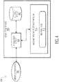
- FIG. 4 is an example system for hosting instructions for enabling a power-domain current balancing apparatus.
- the system 400 shows an input/output data 402 interface with an electronic apparatus 404.
- the electronic apparatus 404 includes a processor 406, a storage device 408, and a non-transient machine-readable storage medium 410.
- the machine-readable storage medium 410 includes instructions 412 which control how the processor 406 receives input data 402 and transforms the input data into output data 402, using data within the storage device 408.
- Example instructions 412 stored in the machine-readable storage medium 410 are discussed elsewhere in this specification.
- the machine-readable storage medium in an alternate example embodiment is a non-transient computer-readable storage medium.
- the processor (such as a central processing unit, CPU, microprocessor, application-specific integrated circuit (ASIC), etc.) controls the overall operation of the storage device (such as random access memory (RAM) for temporary data storage, read only memory (ROM) for permanent data storage, firmware, flash memory, external and internal hard-disk drives, and the like).
- the processor device communicates with the storage device and non-transient machine-readable storage medium using a bus and performs operations and tasks that implement one or more instructions stored in the machine-readable storage medium.
- the machine-readable storage medium in an alternate example embodiment is a computer-readable storage medium.
- the set of instructions described above are implemented as functional and software instructions embodied as a set of executable instructions in a non-transient computer-readable or computer-usable media which are effected on a computer or machine programmed with and controlled by said executable instructions.
- Said instructions are loaded for execution on a processor (such as one or more CPUs).
- Said processor includes microprocessors, microcontrollers, processor modules or subsystems (including one or more microprocessors or microcontrollers), or other control or computing devices.
- a processor can refer to a single component or to plural components.
- Said computer-readable or computer-usable storage medium or media is (are) considered to be part of an article (or article of manufacture).
- An article or article of manufacture can refer to any manufactured single component or multiple components.
- the non-transient machine or computer-usable media or mediums as defined herein excludes signals, but such media or mediums may be capable of receiving and processing information from signals and/or other transient mediums.
- Example embodiments of the material discussed in this specification can be implemented in whole or in part through network, computer, or data based devices and/or services. These may include cloud, internet, intranet, mobile, desktop, processor, look-up table, microcontroller, consumer equipment, infrastructure, or other enabling devices and services. As may be used herein and in the claims, the following non-exclusive definitions are provided.
- one or more instructions or steps discussed herein are automated.
- the terms automated or automatically mean controlled operation of an apparatus, system, and/or process using computers and/or mechanical/electrical devices without the necessity of human intervention, observation, effort and/or decision.
Landscapes
- Engineering & Computer Science (AREA)
- Physics & Mathematics (AREA)
- General Physics & Mathematics (AREA)
- Theoretical Computer Science (AREA)
- General Engineering & Computer Science (AREA)
- Power Engineering (AREA)
- Automation & Control Theory (AREA)
- Electromagnetism (AREA)
- Radar, Positioning & Navigation (AREA)
- Power Sources (AREA)
Claims (11)
- Vorrichtung (100) zur Energieverwaltung, umfassend:eine obere Energiedomäne (102) und eine untere Energiedomäne (108), angeordnet in einer gestapelten Konfiguration;einen Stromsenken-/-Quellensensor (114), ausgelegt zum Überwachen eines Energieversorgung-zu-Zwischen-Energiedomänen-Senken-/-Quellen-Stroms und zum Erzeugen eines Stromfehlanpassungssignals (116), wenn der Energieversorgung-zu-Zwischen-Energiedomänen-Senken-/-Quellen-Strom einen Schwellenbereich überschreitet, wobei der Energieversorgung-zu-Zwischen-Energiedomänen-Senken-/-Quellen-Strom ein Strom ist, der entweder einem elektrischen Knoten zwischen der oberen Energiedomäne (102) und der unteren Energiedomäne (108) zugeführt oder diesem entnommen wird; undeine Stromungleichgewichtssteuerung (124), die so geschaltet ist, dass sie das Stromfehlanpassungssignal (116) empfängt, und ausgelegt ist zum Erzeugen einer Menge von Energiedomänen-Steuersignalen, umfassend:ein Obere-Energiedomäne-Frequenzauswahlsignal und ein Untere-Energiedomäne-Frequenzauswahlsignal, das durch eine Energiedomänen-Frequenzsteuerung erzeugt wird, die mit der Stromungleichgewichtssteuerung gekoppelt ist; undein Obere-Energiedomäne-Spannungsauswahlsignal und ein Untere-Energiedomäne-Spannungsauswahlsignal, das durch eine Energiedomänen-Spannungssteuerung (120) erzeugt wird, die mit der Stromungleichgewichtssteuerung gekoppelt ist,zum Steuern der oberen und unteren Energiedomäne (102, 108), um einen Absolutwert des Energieversorgungzu-Zwischen-Energiedomänen-Senken-/-Quellen-Stroms zu verringern, wobei die Stromungleichgewichtssteuerung ausgelegt ist zum Anvisieren eines Signals verringerter Stromfehlanpassung durch Variieren der Obere-Energiedomäne-Spannungsauswahl, der Untere-Energiedomäne-Spannungsauswahl, der Obere-Energiedomäne-Frequenzauswahl und der Untere-Energiedomäne-Frequenzauswahl unter Berücksichtigung einer oder mehrerer Beschränkungen des Systems, wobei die Beschränkungen des Systems eine oder mehrere der folgenden umfassen:einen Mindestdurchsatz einzelner Energiedomänen;einen kombinierten Gesamtdurchsatz zweier Energiedomänen;eine Spannungsreserve für einzelne Energiedomänen;eine Gesamtreserve für zwei Energiedomänen; undeine zulässige Frequenz als Funktion der Spannung jeder Energiedomäne undwobei die Stromungleichgewichtssteuerung (124) ausgelegt ist zum Anvisieren des Signals verringerter Stromfehlanpassung durch Ändern von mindestens zwei der folgenden:Obere-Energiedomäne-Frequenzauswahl;Untere-Energiedomäne-Frequenzauswahl;Obere-Energiedomäne-Spannungsauswahl; undUntere-Energiedomäne-Spannungsauswahl gemäß einem rekursiven Algorithmus.
- Vorrichtung (100) nach Anspruch 1,
wobei der Schwellenbereich null Ampere umfasst. - Vorrichtung nach Anspruch 1,
wobei sich die obere und untere Energiedomäne in einer gestapelten Konfiguration befinden, die Ladungsrecycling verwendet. - Vorrichtung (100) nach einem der vorhergehenden Ansprüche,
wobei eine der Energiedomänen eine Speicherschaltung und eine andere eine Rechenlogikschaltung ist. - Vorrichtung (100) nach einem der vorhergehenden Ansprüche,
wobei die Menge von Energiedomänen-Steuersignalen mindestens eines von Folgendem umfasst: ein Spannungssteuersignal, ein Frequenzsteuersignal und ein Aufgabensteuersignal. - Vorrichtung (100) nach Anspruch 1,
wobei, wenn das Stromfehlanpassungssignal (116) angibt, dass ein Obere-Energiedomäne-Strom größer als ein Untere-Energiedomäne-Strom ist, das Obere-Energiedomäne-Spannungsauswahlsignal dann eine verringerte Obere-Energiedomäne-Spannung auswählt. - Vorrichtung (100) nach Anspruch 1,
wobei, wenn das Stromfehlanpassungssignal (116) angibt, dass ein Obere-Energiedomäne-Strom größer als ein Untere-Energiedomäne-Strom ist, das Untere-Energiedomäne-Spannungsauswahlsignal dann eine vergrößerte Untere-Energiedomäne-Spannung auswählt. - Vorrichtung (100) nach Anspruch 1,
wobei, wenn das Stromfehlanpassungssignal (116) angibt, dass ein Obere-Energiedomäne-Strom größer als ein Untere-Energiedomäne-Strom ist, das Obere-Energiedomäne-Frequenzauswahlsignal dann eine verringerte Obere-Energiedomäne-Frequenz auswählt. - Vorrichtung (100) nach einem der vorhergehenden Ansprüche,die ferner eine Energiedomänen-Aufgabensteuerung (130) umfasst, die mit der Stromungleichgewichtssteuerung (124) gekoppelt ist,wobei die Menge von Energiedomänen-Steuersignalen ferner ein Obere-Energiedomäne-Aufgabenauswahlsignal und ein Untere-Energiedomäne-Aufgabenauswahlsignal umfasst, das durch die Energiedomänen-Aufgabensteuerung erzeugt wird.
- Vorrichtung (100) nach Anspruch 9,
wobei, wenn das Stromfehlanpassungssignal (116) angibt, dass ein Obere-Energiedomäne-Strom größer als ein Untere-Energiedomäne-Strom ist, das Obere-Energiedomäne-Aufgabenauswahlsignal dann eine verringerte Last von Obere-Energiedomäne-Aufgaben auswählt. - Vorrichtung (100) nach Anspruch 8,
wobei das Aufgabenauswahlsignal mindestens eines von Folgendem umfasst: ein Logikauswahlsignal, ein Firmware-Auswahlsignal oder Software-Ausführungssignal.
Applications Claiming Priority (1)
| Application Number | Priority Date | Filing Date | Title |
|---|---|---|---|
| US14/973,575 US10153639B2 (en) | 2015-12-17 | 2015-12-17 | Power-domain current balance |
Publications (2)
| Publication Number | Publication Date |
|---|---|
| EP3182248A1 EP3182248A1 (de) | 2017-06-21 |
| EP3182248B1 true EP3182248B1 (de) | 2022-12-14 |
Family
ID=57680070
Family Applications (1)
| Application Number | Title | Priority Date | Filing Date |
|---|---|---|---|
| EP16204335.0A Not-in-force EP3182248B1 (de) | 2015-12-17 | 2016-12-15 | Leistungsbereichsstromverteilung |
Country Status (3)
| Country | Link |
|---|---|
| US (1) | US10153639B2 (de) |
| EP (1) | EP3182248B1 (de) |
| CN (1) | CN106896862B (de) |
Families Citing this family (2)
| Publication number | Priority date | Publication date | Assignee | Title |
|---|---|---|---|---|
| CN117950478A (zh) * | 2017-08-22 | 2024-04-30 | 英特尔公司 | 用于计算机设备的基于应用优先级的功率管理 |
| US11550348B2 (en) * | 2021-03-24 | 2023-01-10 | Stmicroelectronics International N.V. | Methods and devices for bypassing a voltage regulator |
Family Cites Families (10)
| Publication number | Priority date | Publication date | Assignee | Title |
|---|---|---|---|---|
| US7329968B2 (en) | 2003-05-08 | 2008-02-12 | The Trustees Of Columbia University In The City Of New York | Charge-recycling voltage domains for energy-efficient low-voltage operation of digital CMOS circuits |
| US7170267B1 (en) * | 2003-08-14 | 2007-01-30 | Volterra Semiconductor Corporation | Switching regulator with average current mode control |
| US8339177B2 (en) | 2011-01-26 | 2012-12-25 | Freescale Semiconductor, Inc. | Multiple function power domain level shifter |
| US8604867B2 (en) * | 2011-11-28 | 2013-12-10 | Qualcomm Incorporated | Energy harvesting in integrated circuit packages |
| WO2013091165A1 (zh) * | 2011-12-20 | 2013-06-27 | Xu Youhong | 电力电网有线供电、基站发射和有源无线接收电能的方法 |
| CN202799296U (zh) * | 2012-08-27 | 2013-03-13 | 北京创世汇科技发展有限公司 | 智能照明能源管理与控制系统 |
| US8797084B2 (en) * | 2012-08-31 | 2014-08-05 | International Business Machines Corporation | Calibration schemes for charge-recycling stacked voltage domains |
| US8984313B2 (en) * | 2012-08-31 | 2015-03-17 | Intel Corporation | Configuring power management functionality in a processor including a plurality of cores by utilizing a register to store a power domain indicator |
| US20150346742A1 (en) | 2014-06-02 | 2015-12-03 | Nxp B.V. | Energy recycling for a cost effective platform to optimize energy efficiency for low powered system |
| EP2953004B1 (de) | 2014-06-02 | 2018-09-26 | Nxp B.V. | Energieverwertung für eine kosteneffektive plattform zur optimierung der energieeffizienz für ein system mit niedrigem stromverbrauch |
-
2015
- 2015-12-17 US US14/973,575 patent/US10153639B2/en active Active
-
2016
- 2016-12-15 CN CN201611164188.9A patent/CN106896862B/zh not_active Expired - Fee Related
- 2016-12-15 EP EP16204335.0A patent/EP3182248B1/de not_active Not-in-force
Non-Patent Citations (2)
| Title |
|---|
| PRADEEP S SHENOY ET AL: "Overcoming the power wall: Connecting voltage domains in series", ENERGY AWARE COMPUTING (ICEAC), 2011 INTERNATIONAL CONFERENCE ON, IEEE, 30 November 2011 (2011-11-30), pages 1 - 6, XP032296830, ISBN: 978-1-4673-0466-5, DOI: 10.1109/ICEAC.2011.6403629 * |
| SHENOY PRADEEP S. ET AL: "Differential Power Processing for DC Systems", IEEE TRANSACTIONS ON POWER ELECTRONICS, vol. 28, no. 4, 1 April 2013 (2013-04-01), USA, pages 1795 - 1806, XP055870315, ISSN: 0885-8993, Retrieved from the Internet <URL:https://ieeexplore.ieee.org/stampPDF/getPDF.jsp?tp=&arnumber=6276262&ref=aHR0cHM6Ly9pZWVleHBsb3JlLmllZWUub3JnL2Fic3RyYWN0L2RvY3VtZW50LzYyNzYyNjI=> [retrieved on 20211204], DOI: 10.1109/TPEL.2012.2214402 * |
Also Published As
| Publication number | Publication date |
|---|---|
| US10153639B2 (en) | 2018-12-11 |
| EP3182248A1 (de) | 2017-06-21 |
| CN106896862B (zh) | 2020-08-28 |
| US20170179719A1 (en) | 2017-06-22 |
| CN106896862A (zh) | 2017-06-27 |
Similar Documents
| Publication | Publication Date | Title |
|---|---|---|
| EP3286813B1 (de) | Leistungskombinierer und ausgleicher | |
| CA2773804C (en) | Bi-directional converter voltage controlled current source for voltage regulation | |
| US9590501B2 (en) | Fast load transient response power supply system using dynamic reference generation | |
| US20170277238A1 (en) | Peak current support for a power rail system via a shared secondary power supply | |
| US10200022B2 (en) | Integrated voltage regulator with in-built process, temperature and aging compensation | |
| EP4164105A1 (de) | Stromversorgung und emulierte strommodussteuerung | |
| US9281699B2 (en) | Electronic device to be powered by alternative power source | |
| US11069925B2 (en) | Heterogeneous battery system and method | |
| US8912771B2 (en) | Power rail regulator to regulate DC rail voltage and output current | |
| CN107786081A (zh) | 电压转换设备及控制电压转换设备的方法 | |
| CN111726000A (zh) | 开关调节器以及包括开关调节器的电子设备 | |
| US9958922B2 (en) | Low ripple mechanism of mode change in switched capacitor voltage regulators | |
| EP3182248B1 (de) | Leistungsbereichsstromverteilung | |
| US11509228B2 (en) | Dynamic regulation resonant power converter | |
| US20170346298A1 (en) | Voltage control system | |
| US11942870B2 (en) | Power supply unit with autonomous input power limiting | |
| US8504851B2 (en) | Electronic device having power consumption adjusting feature | |
| CN107844185B (zh) | 一种电源管理方法及装置 | |
| KR20220107048A (ko) | 칩 프로세스 변화 인식 전력 효율 최적화 | |
| US20110285450A1 (en) | Managing Heat Dissipation While Testing A Power Device | |
| EP2953004B1 (de) | Energieverwertung für eine kosteneffektive plattform zur optimierung der energieeffizienz für ein system mit niedrigem stromverbrauch | |
| US20190339655A1 (en) | Adjusting voltage settings based on electrical components | |
| US20250199594A1 (en) | Dynamic charge rate control of battery powered devices | |
| US20250390124A1 (en) | Power supply circuit with improved power efficiency using multiplexers | |
| US20120020127A1 (en) | Power system with power saving function |
Legal Events
| Date | Code | Title | Description |
|---|---|---|---|
| PUAI | Public reference made under article 153(3) epc to a published international application that has entered the european phase |
Free format text: ORIGINAL CODE: 0009012 |
|
| STAA | Information on the status of an ep patent application or granted ep patent |
Free format text: STATUS: THE APPLICATION HAS BEEN PUBLISHED |
|
| AK | Designated contracting states |
Kind code of ref document: A1 Designated state(s): AL AT BE BG CH CY CZ DE DK EE ES FI FR GB GR HR HU IE IS IT LI LT LU LV MC MK MT NL NO PL PT RO RS SE SI SK SM TR |
|
| AX | Request for extension of the european patent |
Extension state: BA ME |
|
| STAA | Information on the status of an ep patent application or granted ep patent |
Free format text: STATUS: REQUEST FOR EXAMINATION WAS MADE |
|
| 17P | Request for examination filed |
Effective date: 20171221 |
|
| RBV | Designated contracting states (corrected) |
Designated state(s): AL AT BE BG CH CY CZ DE DK EE ES FI FR GB GR HR HU IE IS IT LI LT LU LV MC MK MT NL NO PL PT RO RS SE SI SK SM TR |
|
| STAA | Information on the status of an ep patent application or granted ep patent |
Free format text: STATUS: EXAMINATION IS IN PROGRESS |
|
| 17Q | First examination report despatched |
Effective date: 20200820 |
|
| GRAP | Despatch of communication of intention to grant a patent |
Free format text: ORIGINAL CODE: EPIDOSNIGR1 |
|
| STAA | Information on the status of an ep patent application or granted ep patent |
Free format text: STATUS: GRANT OF PATENT IS INTENDED |
|
| INTG | Intention to grant announced |
Effective date: 20220524 |
|
| RAP3 | Party data changed (applicant data changed or rights of an application transferred) |
Owner name: NXP B.V. |
|
| GRAJ | Information related to disapproval of communication of intention to grant by the applicant or resumption of examination proceedings by the epo deleted |
Free format text: ORIGINAL CODE: EPIDOSDIGR1 |
|
| STAA | Information on the status of an ep patent application or granted ep patent |
Free format text: STATUS: EXAMINATION IS IN PROGRESS |
|
| GRAP | Despatch of communication of intention to grant a patent |
Free format text: ORIGINAL CODE: EPIDOSNIGR1 |
|
| STAA | Information on the status of an ep patent application or granted ep patent |
Free format text: STATUS: GRANT OF PATENT IS INTENDED |
|
| INTC | Intention to grant announced (deleted) | ||
| GRAS | Grant fee paid |
Free format text: ORIGINAL CODE: EPIDOSNIGR3 |
|
| GRAA | (expected) grant |
Free format text: ORIGINAL CODE: 0009210 |
|
| STAA | Information on the status of an ep patent application or granted ep patent |
Free format text: STATUS: THE PATENT HAS BEEN GRANTED |
|
| INTG | Intention to grant announced |
Effective date: 20221021 |
|
| AK | Designated contracting states |
Kind code of ref document: B1 Designated state(s): AL AT BE BG CH CY CZ DE DK EE ES FI FR GB GR HR HU IE IS IT LI LT LU LV MC MK MT NL NO PL PT RO RS SE SI SK SM TR |
|
| REG | Reference to a national code |
Ref country code: GB Ref legal event code: FG4D |
|
| REG | Reference to a national code |
Ref country code: CH Ref legal event code: EP |
|
| REG | Reference to a national code |
Ref country code: DE Ref legal event code: R096 Ref document number: 602016076869 Country of ref document: DE |
|
| REG | Reference to a national code |
Ref country code: IE Ref legal event code: FG4D |
|
| REG | Reference to a national code |
Ref country code: AT Ref legal event code: REF Ref document number: 1538076 Country of ref document: AT Kind code of ref document: T Effective date: 20230115 |
|
| REG | Reference to a national code |
Ref country code: LT Ref legal event code: MG9D |
|
| REG | Reference to a national code |
Ref country code: NL Ref legal event code: MP Effective date: 20221214 |
|
| PG25 | Lapsed in a contracting state [announced via postgrant information from national office to epo] |
Ref country code: SE Free format text: LAPSE BECAUSE OF FAILURE TO SUBMIT A TRANSLATION OF THE DESCRIPTION OR TO PAY THE FEE WITHIN THE PRESCRIBED TIME-LIMIT Effective date: 20221214 Ref country code: NO Free format text: LAPSE BECAUSE OF FAILURE TO SUBMIT A TRANSLATION OF THE DESCRIPTION OR TO PAY THE FEE WITHIN THE PRESCRIBED TIME-LIMIT Effective date: 20230314 Ref country code: LT Free format text: LAPSE BECAUSE OF FAILURE TO SUBMIT A TRANSLATION OF THE DESCRIPTION OR TO PAY THE FEE WITHIN THE PRESCRIBED TIME-LIMIT Effective date: 20221214 Ref country code: FI Free format text: LAPSE BECAUSE OF FAILURE TO SUBMIT A TRANSLATION OF THE DESCRIPTION OR TO PAY THE FEE WITHIN THE PRESCRIBED TIME-LIMIT Effective date: 20221214 |
|
| REG | Reference to a national code |
Ref country code: AT Ref legal event code: MK05 Ref document number: 1538076 Country of ref document: AT Kind code of ref document: T Effective date: 20221214 |
|
| PG25 | Lapsed in a contracting state [announced via postgrant information from national office to epo] |
Ref country code: RS Free format text: LAPSE BECAUSE OF FAILURE TO SUBMIT A TRANSLATION OF THE DESCRIPTION OR TO PAY THE FEE WITHIN THE PRESCRIBED TIME-LIMIT Effective date: 20221214 Ref country code: LV Free format text: LAPSE BECAUSE OF FAILURE TO SUBMIT A TRANSLATION OF THE DESCRIPTION OR TO PAY THE FEE WITHIN THE PRESCRIBED TIME-LIMIT Effective date: 20221214 Ref country code: HR Free format text: LAPSE BECAUSE OF FAILURE TO SUBMIT A TRANSLATION OF THE DESCRIPTION OR TO PAY THE FEE WITHIN THE PRESCRIBED TIME-LIMIT Effective date: 20221214 Ref country code: GR Free format text: LAPSE BECAUSE OF FAILURE TO SUBMIT A TRANSLATION OF THE DESCRIPTION OR TO PAY THE FEE WITHIN THE PRESCRIBED TIME-LIMIT Effective date: 20230315 |
|
| PG25 | Lapsed in a contracting state [announced via postgrant information from national office to epo] |
Ref country code: NL Free format text: LAPSE BECAUSE OF FAILURE TO SUBMIT A TRANSLATION OF THE DESCRIPTION OR TO PAY THE FEE WITHIN THE PRESCRIBED TIME-LIMIT Effective date: 20221214 |
|
| PG25 | Lapsed in a contracting state [announced via postgrant information from national office to epo] |
Ref country code: SM Free format text: LAPSE BECAUSE OF FAILURE TO SUBMIT A TRANSLATION OF THE DESCRIPTION OR TO PAY THE FEE WITHIN THE PRESCRIBED TIME-LIMIT Effective date: 20221214 Ref country code: RO Free format text: LAPSE BECAUSE OF FAILURE TO SUBMIT A TRANSLATION OF THE DESCRIPTION OR TO PAY THE FEE WITHIN THE PRESCRIBED TIME-LIMIT Effective date: 20221214 Ref country code: PT Free format text: LAPSE BECAUSE OF FAILURE TO SUBMIT A TRANSLATION OF THE DESCRIPTION OR TO PAY THE FEE WITHIN THE PRESCRIBED TIME-LIMIT Effective date: 20230414 Ref country code: ES Free format text: LAPSE BECAUSE OF FAILURE TO SUBMIT A TRANSLATION OF THE DESCRIPTION OR TO PAY THE FEE WITHIN THE PRESCRIBED TIME-LIMIT Effective date: 20221214 Ref country code: EE Free format text: LAPSE BECAUSE OF FAILURE TO SUBMIT A TRANSLATION OF THE DESCRIPTION OR TO PAY THE FEE WITHIN THE PRESCRIBED TIME-LIMIT Effective date: 20221214 Ref country code: CZ Free format text: LAPSE BECAUSE OF FAILURE TO SUBMIT A TRANSLATION OF THE DESCRIPTION OR TO PAY THE FEE WITHIN THE PRESCRIBED TIME-LIMIT Effective date: 20221214 Ref country code: AT Free format text: LAPSE BECAUSE OF FAILURE TO SUBMIT A TRANSLATION OF THE DESCRIPTION OR TO PAY THE FEE WITHIN THE PRESCRIBED TIME-LIMIT Effective date: 20221214 |
|
| REG | Reference to a national code |
Ref country code: CH Ref legal event code: PL |
|
| REG | Reference to a national code |
Ref country code: BE Ref legal event code: MM Effective date: 20221231 |
|
| P01 | Opt-out of the competence of the unified patent court (upc) registered |
Effective date: 20230725 |
|
| PG25 | Lapsed in a contracting state [announced via postgrant information from national office to epo] |
Ref country code: SK Free format text: LAPSE BECAUSE OF FAILURE TO SUBMIT A TRANSLATION OF THE DESCRIPTION OR TO PAY THE FEE WITHIN THE PRESCRIBED TIME-LIMIT Effective date: 20221214 Ref country code: PL Free format text: LAPSE BECAUSE OF FAILURE TO SUBMIT A TRANSLATION OF THE DESCRIPTION OR TO PAY THE FEE WITHIN THE PRESCRIBED TIME-LIMIT Effective date: 20221214 Ref country code: LU Free format text: LAPSE BECAUSE OF NON-PAYMENT OF DUE FEES Effective date: 20221215 Ref country code: IS Free format text: LAPSE BECAUSE OF FAILURE TO SUBMIT A TRANSLATION OF THE DESCRIPTION OR TO PAY THE FEE WITHIN THE PRESCRIBED TIME-LIMIT Effective date: 20230414 Ref country code: AL Free format text: LAPSE BECAUSE OF FAILURE TO SUBMIT A TRANSLATION OF THE DESCRIPTION OR TO PAY THE FEE WITHIN THE PRESCRIBED TIME-LIMIT Effective date: 20221214 |
|
| REG | Reference to a national code |
Ref country code: DE Ref legal event code: R097 Ref document number: 602016076869 Country of ref document: DE |
|
| PG25 | Lapsed in a contracting state [announced via postgrant information from national office to epo] |
Ref country code: MC Free format text: LAPSE BECAUSE OF FAILURE TO SUBMIT A TRANSLATION OF THE DESCRIPTION OR TO PAY THE FEE WITHIN THE PRESCRIBED TIME-LIMIT Effective date: 20221214 |
|
| PLBE | No opposition filed within time limit |
Free format text: ORIGINAL CODE: 0009261 |
|
| STAA | Information on the status of an ep patent application or granted ep patent |
Free format text: STATUS: NO OPPOSITION FILED WITHIN TIME LIMIT |
|
| PG25 | Lapsed in a contracting state [announced via postgrant information from national office to epo] |
Ref country code: LI Free format text: LAPSE BECAUSE OF NON-PAYMENT OF DUE FEES Effective date: 20221231 Ref country code: IE Free format text: LAPSE BECAUSE OF NON-PAYMENT OF DUE FEES Effective date: 20221215 Ref country code: DK Free format text: LAPSE BECAUSE OF FAILURE TO SUBMIT A TRANSLATION OF THE DESCRIPTION OR TO PAY THE FEE WITHIN THE PRESCRIBED TIME-LIMIT Effective date: 20221214 Ref country code: CH Free format text: LAPSE BECAUSE OF NON-PAYMENT OF DUE FEES Effective date: 20221231 |
|
| 26N | No opposition filed |
Effective date: 20230915 |
|
| GBPC | Gb: european patent ceased through non-payment of renewal fee |
Effective date: 20230314 |
|
| PG25 | Lapsed in a contracting state [announced via postgrant information from national office to epo] |
Ref country code: SI Free format text: LAPSE BECAUSE OF FAILURE TO SUBMIT A TRANSLATION OF THE DESCRIPTION OR TO PAY THE FEE WITHIN THE PRESCRIBED TIME-LIMIT Effective date: 20221214 Ref country code: BE Free format text: LAPSE BECAUSE OF NON-PAYMENT OF DUE FEES Effective date: 20221231 |
|
| PG25 | Lapsed in a contracting state [announced via postgrant information from national office to epo] |
Ref country code: GB Free format text: LAPSE BECAUSE OF NON-PAYMENT OF DUE FEES Effective date: 20230314 |
|
| PG25 | Lapsed in a contracting state [announced via postgrant information from national office to epo] |
Ref country code: GB Free format text: LAPSE BECAUSE OF NON-PAYMENT OF DUE FEES Effective date: 20230314 Ref country code: FR Free format text: LAPSE BECAUSE OF NON-PAYMENT OF DUE FEES Effective date: 20230214 |
|
| PGFP | Annual fee paid to national office [announced via postgrant information from national office to epo] |
Ref country code: DE Payment date: 20231121 Year of fee payment: 8 |
|
| PG25 | Lapsed in a contracting state [announced via postgrant information from national office to epo] |
Ref country code: HU Free format text: LAPSE BECAUSE OF FAILURE TO SUBMIT A TRANSLATION OF THE DESCRIPTION OR TO PAY THE FEE WITHIN THE PRESCRIBED TIME-LIMIT; INVALID AB INITIO Effective date: 20161215 |
|
| PG25 | Lapsed in a contracting state [announced via postgrant information from national office to epo] |
Ref country code: CY Free format text: LAPSE BECAUSE OF FAILURE TO SUBMIT A TRANSLATION OF THE DESCRIPTION OR TO PAY THE FEE WITHIN THE PRESCRIBED TIME-LIMIT Effective date: 20221214 |
|
| PG25 | Lapsed in a contracting state [announced via postgrant information from national office to epo] |
Ref country code: MK Free format text: LAPSE BECAUSE OF FAILURE TO SUBMIT A TRANSLATION OF THE DESCRIPTION OR TO PAY THE FEE WITHIN THE PRESCRIBED TIME-LIMIT Effective date: 20221214 Ref country code: IT Free format text: LAPSE BECAUSE OF FAILURE TO SUBMIT A TRANSLATION OF THE DESCRIPTION OR TO PAY THE FEE WITHIN THE PRESCRIBED TIME-LIMIT Effective date: 20221214 |
|
| PG25 | Lapsed in a contracting state [announced via postgrant information from national office to epo] |
Ref country code: BG Free format text: LAPSE BECAUSE OF FAILURE TO SUBMIT A TRANSLATION OF THE DESCRIPTION OR TO PAY THE FEE WITHIN THE PRESCRIBED TIME-LIMIT Effective date: 20221214 |
|
| PG25 | Lapsed in a contracting state [announced via postgrant information from national office to epo] |
Ref country code: MT Free format text: LAPSE BECAUSE OF FAILURE TO SUBMIT A TRANSLATION OF THE DESCRIPTION OR TO PAY THE FEE WITHIN THE PRESCRIBED TIME-LIMIT Effective date: 20221214 |
|
| REG | Reference to a national code |
Ref country code: DE Ref legal event code: R119 Ref document number: 602016076869 Country of ref document: DE |
|
| PG25 | Lapsed in a contracting state [announced via postgrant information from national office to epo] |
Ref country code: DE Free format text: LAPSE BECAUSE OF NON-PAYMENT OF DUE FEES Effective date: 20250701 |
|
| PG25 | Lapsed in a contracting state [announced via postgrant information from national office to epo] |
Ref country code: TR Free format text: LAPSE BECAUSE OF FAILURE TO SUBMIT A TRANSLATION OF THE DESCRIPTION OR TO PAY THE FEE WITHIN THE PRESCRIBED TIME-LIMIT Effective date: 20221214 |