EP3185236B1 - Goa-schaltung und ansteuerungsverfahren dafür sowie anzeigevorrichtung - Google Patents
Goa-schaltung und ansteuerungsverfahren dafür sowie anzeigevorrichtung Download PDFInfo
- Publication number
- EP3185236B1 EP3185236B1 EP14884262.8A EP14884262A EP3185236B1 EP 3185236 B1 EP3185236 B1 EP 3185236B1 EP 14884262 A EP14884262 A EP 14884262A EP 3185236 B1 EP3185236 B1 EP 3185236B1
- Authority
- EP
- European Patent Office
- Prior art keywords
- goa
- drive line
- line scan
- group
- signal generation
- Prior art date
- Legal status (The legal status is an assumption and is not a legal conclusion. Google has not performed a legal analysis and makes no representation as to the accuracy of the status listed.)
- Active
Links
Images

Classifications
-
- G—PHYSICS
- G06—COMPUTING OR CALCULATING; COUNTING
- G06F—ELECTRIC DIGITAL DATA PROCESSING
- G06F3/00—Input arrangements for transferring data to be processed into a form capable of being handled by the computer; Output arrangements for transferring data from processing unit to output unit, e.g. interface arrangements
- G06F3/01—Input arrangements or combined input and output arrangements for interaction between user and computer
- G06F3/03—Arrangements for converting the position or the displacement of a member into a coded form
- G06F3/041—Digitisers, e.g. for touch screens or touch pads, characterised by the transducing means
- G06F3/0412—Digitisers structurally integrated in a display
-
- G—PHYSICS
- G06—COMPUTING OR CALCULATING; COUNTING
- G06F—ELECTRIC DIGITAL DATA PROCESSING
- G06F3/00—Input arrangements for transferring data to be processed into a form capable of being handled by the computer; Output arrangements for transferring data from processing unit to output unit, e.g. interface arrangements
- G06F3/01—Input arrangements or combined input and output arrangements for interaction between user and computer
- G06F3/03—Arrangements for converting the position or the displacement of a member into a coded form
- G06F3/041—Digitisers, e.g. for touch screens or touch pads, characterised by the transducing means
- G06F3/0416—Control or interface arrangements specially adapted for digitisers
- G06F3/04164—Connections between sensors and controllers, e.g. routing lines between electrodes and connection pads
-
- G—PHYSICS
- G06—COMPUTING OR CALCULATING; COUNTING
- G06F—ELECTRIC DIGITAL DATA PROCESSING
- G06F3/00—Input arrangements for transferring data to be processed into a form capable of being handled by the computer; Output arrangements for transferring data from processing unit to output unit, e.g. interface arrangements
- G06F3/01—Input arrangements or combined input and output arrangements for interaction between user and computer
- G06F3/03—Arrangements for converting the position or the displacement of a member into a coded form
- G06F3/041—Digitisers, e.g. for touch screens or touch pads, characterised by the transducing means
- G06F3/0416—Control or interface arrangements specially adapted for digitisers
- G06F3/0418—Control or interface arrangements specially adapted for digitisers for error correction or compensation, e.g. based on parallax, calibration or alignment
- G06F3/04184—Synchronisation with the driving of the display or the backlighting unit to avoid interferences generated internally
-
- G—PHYSICS
- G09—EDUCATION; CRYPTOGRAPHY; DISPLAY; ADVERTISING; SEALS
- G09G—ARRANGEMENTS OR CIRCUITS FOR CONTROL OF INDICATING DEVICES USING STATIC MEANS TO PRESENT VARIABLE INFORMATION
- G09G3/00—Control arrangements or circuits, of interest only in connection with visual indicators other than cathode-ray tubes
- G09G3/20—Control arrangements or circuits, of interest only in connection with visual indicators other than cathode-ray tubes for presentation of an assembly of a number of characters, e.g. a page, by composing the assembly by combination of individual elements arranged in a matrix no fixed position being assigned to or needed to be assigned to the individual characters or partial characters
- G09G3/22—Control arrangements or circuits, of interest only in connection with visual indicators other than cathode-ray tubes for presentation of an assembly of a number of characters, e.g. a page, by composing the assembly by combination of individual elements arranged in a matrix no fixed position being assigned to or needed to be assigned to the individual characters or partial characters using controlled light sources
- G09G3/30—Control arrangements or circuits, of interest only in connection with visual indicators other than cathode-ray tubes for presentation of an assembly of a number of characters, e.g. a page, by composing the assembly by combination of individual elements arranged in a matrix no fixed position being assigned to or needed to be assigned to the individual characters or partial characters using controlled light sources using electroluminescent panels
- G09G3/32—Control arrangements or circuits, of interest only in connection with visual indicators other than cathode-ray tubes for presentation of an assembly of a number of characters, e.g. a page, by composing the assembly by combination of individual elements arranged in a matrix no fixed position being assigned to or needed to be assigned to the individual characters or partial characters using controlled light sources using electroluminescent panels semiconductive, e.g. using light-emitting diodes [LED]
- G09G3/3208—Control arrangements or circuits, of interest only in connection with visual indicators other than cathode-ray tubes for presentation of an assembly of a number of characters, e.g. a page, by composing the assembly by combination of individual elements arranged in a matrix no fixed position being assigned to or needed to be assigned to the individual characters or partial characters using controlled light sources using electroluminescent panels semiconductive, e.g. using light-emitting diodes [LED] organic, e.g. using organic light-emitting diodes [OLED]
- G09G3/3225—Control arrangements or circuits, of interest only in connection with visual indicators other than cathode-ray tubes for presentation of an assembly of a number of characters, e.g. a page, by composing the assembly by combination of individual elements arranged in a matrix no fixed position being assigned to or needed to be assigned to the individual characters or partial characters using controlled light sources using electroluminescent panels semiconductive, e.g. using light-emitting diodes [LED] organic, e.g. using organic light-emitting diodes [OLED] using an active matrix
-
- G—PHYSICS
- G11—INFORMATION STORAGE
- G11C—STATIC STORES
- G11C19/00—Digital stores in which the information is moved stepwise, e.g. shift registers
-
- G—PHYSICS
- G09—EDUCATION; CRYPTOGRAPHY; DISPLAY; ADVERTISING; SEALS
- G09G—ARRANGEMENTS OR CIRCUITS FOR CONTROL OF INDICATING DEVICES USING STATIC MEANS TO PRESENT VARIABLE INFORMATION
- G09G2310/00—Command of the display device
- G09G2310/02—Addressing, scanning or driving the display screen or processing steps related thereto
- G09G2310/0264—Details of driving circuits
- G09G2310/0286—Details of a shift registers arranged for use in a driving circuit
-
- G—PHYSICS
- G09—EDUCATION; CRYPTOGRAPHY; DISPLAY; ADVERTISING; SEALS
- G09G—ARRANGEMENTS OR CIRCUITS FOR CONTROL OF INDICATING DEVICES USING STATIC MEANS TO PRESENT VARIABLE INFORMATION
- G09G2330/00—Aspects of power supply; Aspects of display protection and defect management
- G09G2330/02—Details of power systems and of start or stop of display operation
- G09G2330/021—Power management, e.g. power saving
-
- G—PHYSICS
- G09—EDUCATION; CRYPTOGRAPHY; DISPLAY; ADVERTISING; SEALS
- G09G—ARRANGEMENTS OR CIRCUITS FOR CONTROL OF INDICATING DEVICES USING STATIC MEANS TO PRESENT VARIABLE INFORMATION
- G09G3/00—Control arrangements or circuits, of interest only in connection with visual indicators other than cathode-ray tubes
- G09G3/20—Control arrangements or circuits, of interest only in connection with visual indicators other than cathode-ray tubes for presentation of an assembly of a number of characters, e.g. a page, by composing the assembly by combination of individual elements arranged in a matrix no fixed position being assigned to or needed to be assigned to the individual characters or partial characters
-
- G—PHYSICS
- G09—EDUCATION; CRYPTOGRAPHY; DISPLAY; ADVERTISING; SEALS
- G09G—ARRANGEMENTS OR CIRCUITS FOR CONTROL OF INDICATING DEVICES USING STATIC MEANS TO PRESENT VARIABLE INFORMATION
- G09G3/00—Control arrangements or circuits, of interest only in connection with visual indicators other than cathode-ray tubes
- G09G3/20—Control arrangements or circuits, of interest only in connection with visual indicators other than cathode-ray tubes for presentation of an assembly of a number of characters, e.g. a page, by composing the assembly by combination of individual elements arranged in a matrix no fixed position being assigned to or needed to be assigned to the individual characters or partial characters
- G09G3/22—Control arrangements or circuits, of interest only in connection with visual indicators other than cathode-ray tubes for presentation of an assembly of a number of characters, e.g. a page, by composing the assembly by combination of individual elements arranged in a matrix no fixed position being assigned to or needed to be assigned to the individual characters or partial characters using controlled light sources
- G09G3/30—Control arrangements or circuits, of interest only in connection with visual indicators other than cathode-ray tubes for presentation of an assembly of a number of characters, e.g. a page, by composing the assembly by combination of individual elements arranged in a matrix no fixed position being assigned to or needed to be assigned to the individual characters or partial characters using controlled light sources using electroluminescent panels
- G09G3/32—Control arrangements or circuits, of interest only in connection with visual indicators other than cathode-ray tubes for presentation of an assembly of a number of characters, e.g. a page, by composing the assembly by combination of individual elements arranged in a matrix no fixed position being assigned to or needed to be assigned to the individual characters or partial characters using controlled light sources using electroluminescent panels semiconductive, e.g. using light-emitting diodes [LED]
- G09G3/3208—Control arrangements or circuits, of interest only in connection with visual indicators other than cathode-ray tubes for presentation of an assembly of a number of characters, e.g. a page, by composing the assembly by combination of individual elements arranged in a matrix no fixed position being assigned to or needed to be assigned to the individual characters or partial characters using controlled light sources using electroluminescent panels semiconductive, e.g. using light-emitting diodes [LED] organic, e.g. using organic light-emitting diodes [OLED]
- G09G3/3266—Details of drivers for scan electrodes
-
- G—PHYSICS
- G09—EDUCATION; CRYPTOGRAPHY; DISPLAY; ADVERTISING; SEALS
- G09G—ARRANGEMENTS OR CIRCUITS FOR CONTROL OF INDICATING DEVICES USING STATIC MEANS TO PRESENT VARIABLE INFORMATION
- G09G3/00—Control arrangements or circuits, of interest only in connection with visual indicators other than cathode-ray tubes
- G09G3/20—Control arrangements or circuits, of interest only in connection with visual indicators other than cathode-ray tubes for presentation of an assembly of a number of characters, e.g. a page, by composing the assembly by combination of individual elements arranged in a matrix no fixed position being assigned to or needed to be assigned to the individual characters or partial characters
- G09G3/34—Control arrangements or circuits, of interest only in connection with visual indicators other than cathode-ray tubes for presentation of an assembly of a number of characters, e.g. a page, by composing the assembly by combination of individual elements arranged in a matrix no fixed position being assigned to or needed to be assigned to the individual characters or partial characters by control of light from an independent source
- G09G3/36—Control arrangements or circuits, of interest only in connection with visual indicators other than cathode-ray tubes for presentation of an assembly of a number of characters, e.g. a page, by composing the assembly by combination of individual elements arranged in a matrix no fixed position being assigned to or needed to be assigned to the individual characters or partial characters by control of light from an independent source using liquid crystals
- G09G3/3611—Control of matrices with row and column drivers
- G09G3/3674—Details of drivers for scan electrodes
- G09G3/3677—Details of drivers for scan electrodes suitable for active matrices only
-
- G—PHYSICS
- G11—INFORMATION STORAGE
- G11C—STATIC STORES
- G11C19/00—Digital stores in which the information is moved stepwise, e.g. shift registers
- G11C19/28—Digital stores in which the information is moved stepwise, e.g. shift registers using semiconductor elements
- G11C19/287—Organisation of a multiplicity of shift registers
Definitions
- the present disclosure relates to a GOA (Gate Driver on Array) circuit, a driving method thereof, and a display apparatus.
- GOA Gate Driver on Array
- a touch panel is not necessary to be laminated and assembled with a display panel, but is integrated into the display panel, so that the display panel per se has a touch function.
- the In Cell Touch display panel has advantages in that, a manufacture of a touch element can be completed in a standard manufacture process of the display panel, there is no problem in lamination and alignment, the product is thinner and lighter without a frame, and a pure flat plane design can be achieved.
- the In Cell Touch display panel has become one of hot spots in research in the field.
- a touch function layer of which for realizing the touch function comprises two layers of signal lines vertically with each other, wherein one layer of the signal lines is a drive line (Tx line), and the other layer of the signal lines is a sensing line (Rx Line).
- Tx line drive line
- Rx Line sensing line
- Each drive line is driven in turn by scanning.
- the sensing lines intersected with the drive lines are scanned progressively. It is determined whether the capacitive coupling phenomenon occurs at a certain point or not, so that the accurate touch point location is obtained and the touch function is realized.
- CN 103823589 A discloses a touch circuit, a drive method of the touch circuit and a touch display device The document discloses the features of the preamble of claim 1.
- a Gate Driver on Array (GOA) circuit comprising: a drive line scan control signal generation unit configured to generate a drive line scan clock signal and a drive line scan pulse signal; multiple GOA groups connected with the drive line scan control signal generation unit and connected in series with each other sequentially, which are configured to acquire the drive line scan clock signal, to generate GOA group output signals sequentially according to GOA group input signals, wherein the GOA group output signal generated by one of the GOA groups is the GOA group input signal of a next GOA group so as to realize a shift register function of the multiple GOA groups; multiple drive line scan signal generation groups connected with the multiple GOA groups respectively and connected with the drive line scan control signal generation unit, which are configured to acquire the GOA group output signals and the drive line scan pulse signal, and to generate drive line scan signals sequentially; multiple gate line groups connected with the multiple drive line scan signal generation groups respectively, which are configured to be applied with the drive line scan signals, so as to complete drive line scan for the multiple gate line groups sequentially, wherein a voltage
- each of the multiple GOA groups comprises the same number of multiple GOA units
- the drive line scan signal generation group comprises the same number of multiple drive line scan signal generation units
- the gate line group comprises the same number of multiple gate lines; the numbers of GOA units involved in the drive line scan in each GOA group are the same and are plural.
- output signals of the GOA units involved in the drive line scan in one of the GOA groups are connected through a diode, to form the GOA group output signal as the GOA group input signal for the next GOA group.
- the numbers of the GOA units not involved in the drive line scan spaced between two adjacent GOA units involved in the drive line scan are the same.
- all the GOA units in each of the multiple GOA groups are connected with one of the gate lines through one of the drive line scan signal generation units.
- the drive line scan control signal generation unit is connected with the GOA unit involved in the drive line scan through a diode, to ensure a unidirectional input of the drive line scan clock signal and to prevent a short circuit between the GOA units.
- the drive line scan signal generation unit comprises an AND gate circuit, or the drive line scan signal generation unit comprises an NAND gate circuit and a NOT gate circuit.
- a clock cycle of the drive line scan clock signal is set as time necessary for completing the scan for one drive line;
- a pulse width of the drive line scan pulse signal is set as a pulse width necessary for performing a touch scan.
- the drive line scan clock signal includes a first drive line scan clock signal and a second drive line scan clock signal with reverse phases.
- the drive line scan control signal generation unit is further configured to generate an original input signal for the drive line scan, as the GOA group input signal for the first GOA group.
- a display apparatus is further provided in a further embodiment of the present disclosure, comprising the GOA circuit as described above.
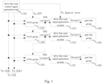
- a GOA circuit comprising: a drive line scan control signal generation unit 101 operative to generate a drive line scan clock signal Tx_CLK and a drive line scan pulse signal Tx_Square wave; multiple GOA groups 102 connected with the drive line scan control signal generation unit 101 and connected in series with each other sequentially, which arc operative to acquire the drive line scan clock signal Tx CLK, to generate GOA group output signals (i.e., GOA output1 ⁇ GOA outputN) sequentially according to GOA group input signals, wherein the GOA group output signal generated by one of the GOA groups 102 is the GOA group input signal of the next GOA group 102 so as to realize a shift register function of the multiple GOA groups; multiple drive line scan signal generation modules 103 connected with the multiple GOA groups 102 respectively and connected with the drive line scan control signal generation unit 101, which are operative to acquire the GOA group output signals (i.e., GOA output1 ⁇ GOA outputN) and the
- the original GOA circuit comprises multiple GOA units in series with each other sequentially, the output terminal of each GOA unit is connected to one of the gate lines, the output terminal of one GOA unit is connected with the input terminal of the next GOA unit, so that the output signal of one GOA unit can be taken as the input signal of the next GOA unit.
- the shift register function of the individual GOA units may be realized.
- the gate lines connected with the individual GOA units are scanned progressively.
- the GOA circuit described above in the present embodiments divides multiple GOA units into multiple GOA groups 102 in order, based on the original structure, so that the gate lines connected with the individual GOA units are divided into multiple gate line groups 104 in order. It can be seen that there is also the shift register function between the individual GOA groups 102 in the present embodiment.
- the drive line scan control signal generation unit 101 is connected with the input terminal of the GOA group 102 to generate Tx CLK and Tx_Square wave, wherein a clock cycle of Tx_CLK is time necessary for completing the scan for one drive line, i.e., the cycle of the drive line scan signal finally generated; and a pulse width of Tx_Square wave is a pulse width necessary for performing a touch scan, i.e., the pulse width of the drive line scan signal finally generated.
- the drive line scan signal generation module 103 is added between the GOA group 102 and the gate line group 104, to combine the GOA group output signal in which the cycle of the drive line scan signal is specified, with Tx_Square wave in which the pulse width of the drive line scan signal is specified, to generate the drive line scan signal necessary for scanning the drive line when performing the touch scan.
- the drive line scan signals Output1 ⁇ OutputN are generated group by group, which are applied to the connected gate line groups 104 so as to achieve the group-wise scan of the gate line groups 104.
- the GOA circuit provided in present embodiment may further comprise a display scan control signal generation unit.
- the display scan control signal generation unit is connected to the individual GOA units in the multiple GOA groups 102, and is used for providing the display scan control signal to the GOA units, so that the individual GOA units generate the display scan signals which are applied to the gate lines connected thereto, to realize the scan of the gate lines, to realize the shift register of the individual GOA units, and to scan all the gate lines progressively.
- the drive line scan control signal generation unit 101 may also be used to generate the original input signal Tx_STV for the drive line scan, which is the GOA group input signal of the first GOA group 102.
- the original input signal Tx_STV for the drive line scan may also be generated using the display scan control signal generation unit, and is not limited here in the present embodiment.
- the GOA circuit provided in the present embodiments realizes the scan function with the gate line as the drive line in the touch scan period of one frame, using the shift register function of the GOA circuit, by adding the drive line scan control signal generation unit 101 and the drive line scan signal generation module 103 into the original GOA circuit. No additional drive circuit necessary for the drive line scan is required, thereby, the area and the number of pins in the chip are decreased, and the cost of the chip is reduced.
- the peripheral wirings for connecting the internal drive line with the external drive circuit is saved, which is helpful in a narrow frame of the display panel.
- the gate line is connected with the GOA circuit inside of the display panel directly, and it does not need to be connected with the external drive circuit through the peripheral circuit, which is helpful to decrease the signal delay and to save the power consumption.
- a driving method for the GOA circuit described above comprising: in a touch scan period of one frame, generating a drive line scan clock signal Tx_CLK and a drive line scan pulse signal Tx_Square wave using the drive line scan control signal generation unit 101; acquiring the drive line scan clock signal Tx CLK and generating GOA group output signals (i.e., GOA output1 ⁇ GOA outputN) sequentially according to GOA group input signals, using the multiple GOA groups, wherein the GOA group output signal generated by one of the GOA groups 102 is the GOA group input signal of the next GOA group so as to realize a shift register function of the multiple GOA groups 102; acquiring the GOA group output signals (i.e., GOA output1 ⁇ GOA outputN) and the drive line scan pulse signal Tx_Square wave, and generating drive line scan signals (i.e., Output1 ⁇ OutputN) sequentially, using the multiple drive line scan signal generation modules 103; applying the drive line
- the time of one frame is divided into the display scan period and the touch scan period. After all the gate lines have been scanned progressively and all the pixels connected with the gate lines have been charged, the display scan period ends, and it enters the touch scan period.
- the touch scan period by specifying the cycle of the drive line scan signal using Tx_CLK which is introduced additionally, specifying the pulse width of the drive line scan signal using Tx_Square wave, and using the shift register function between the individual GOA groups to scan the individual gate line groups 104 group by group, the time division multiplexing of gate lines is realized, so that the GOA circuit has both the pixel drive function and the touch scan function.
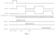
- Step 1 ⁇ Step 4 the driving method for the GOA circuit provided in the present embodiment is described with reference to the timing chart shown in Fig. 2 .
- operations of Step 1 ⁇ Step 4 are performed sequentially.
- Step 1 in a pixel charge time, i.e., the display scan period, the touch scan control signal Tx_CLK (i.e., Tx_CLK1 and Tx_CLK2) and Tx_STV are at a low level, and Tx_Square wave is at a high level.
- Tx_CLK i.e., Tx_CLK1 and Tx_CLK2
- Tx_STV are at a low level
- Tx_Square wave is at a high level.
- the individual GOA units in the circuit are in operation normally and are all involved in the display scan.
- the individual gate lines connected with the individual GOA units are scanned progressively.
- the Thin-Film Transistor (TFT) is turned on to complete the charge to all the pixels.
- Step 2 the charge to the pixels has been finished, and it begins to perform the touch scan.
- Tx_STV is input as the GOA group input signal of the first GOA group, and at the same time it begins to input the drive line scan clock signal Tx CLK, the clock cycle of which is the time for allocating one row of drive line scan, and Tx_Square wave begins to output the square wave, the pulse width of which is about the pulse width required for the touch scan signal, generally between several microseconds to several tens of microseconds.
- the scan for one row of drive line comprises multiple pulses.
- Step 3 the shift register function is realized in the first GOA group.
- the GOA group output signal output by the first GOA group and Tx_Square wave form the pulse square wave necessary for the drive line scan, i.e., the drive line scan signal Output1 which is output, through the drive line scan signal generation module 103.
- the GOA group output signal output by the first GOA group is taken as the GOA group input signal of the second GOA group.
- Step 4 the shift register function is realized in the second GOA group.
- the pulse square wave begins to be output at Output2, and the shift register are performed in subsequent GOA groups in order, the Outputs arc turned on group by group, until the scan of all Outputs are finished.
- the process in one frame is completed, and the pixels in the next frame begin to be charged.
- the entire structure of the GOA circuit and the driving method thereof provided in the present embodiment have been described above.
- the connection relationship between the single GOA group 102 and the drive line scan signal generation module 103 as well as the gate line group 104 connected thereto in the circuit is not limited.
- the accuracy degree of determining the touch point which is necessary for the touch scan does not need to reach the accuracy degree which can be achieved in the drive line scan for each gate line. That is, when the gate lines are multiplexed for the drive line scan, it is not required to scan each gate line progressively.
- the GOA group 102 may comprise at least one GOA unit
- the drive line scan signal generation module 103 may comprise at least one drive line scan signal generation unit
- the gate line group 104 may comprise at least one gate line.
- At least one GOA unit in the GOA group 102 is connected with the drive line scan control signal generation unit to be involved in the drive line scan.
- Each of the GOA units involved in the drive line scan is connected with one of the gate lines through one of the drive line scan signal generation units.
- a part of GOA units and the gate lines connected thereto may be selected from all the GOA units and the gate lines connected thereto (the number of GOA units and that of the gate lines are the same, and the GOA units are connected to the gate lines respectively), to be involved in the drive line scan, and the GOA units and the gate lines connected thereto which arc involved in the drive line scan are configured with the drive line scan signal generation unit to satisfy the requirement for accuracy degree of the touch scan.
- the number of the GOA units and the gate lines which are selected to be involved in the drive line scan may be determined depending on the requirement for accuracy degree of the touch scan. If the requirement for accuracy degree of the touch scan is relatively high, more, even all of, GOA units and gate lines may be selected for the drive line scan. If the requirement for accuracy degree of the touch scan is not very high, but it requires a relatively strict control of the manufacture cost, less GOA units and gate lines may be selected for the drive line scan to further simplify the circuit, reduce the chip area and decrease the chip cost.
- the distribution of the gate lines corresponding to the selected GOA units on the display panel may be arranged according to the actual touch requirement. For example, the touch to the upper or lower region of the display panel may be less than that to the middle region of the display panel. Therefore, more gate lines and corresponding GOA units in the middle region may be selected, so that the gate lines involved in the drive line scan is distributed denser in the middle region of the display panel, than in the upper or lower region, so as to satisfy the requirement for more and more accurate touch operations on the middle region.
- the number of GOA units and that of gate lines in the present embodiment are the same and are in a one-one correspondence, but the number of drive line scan signal generation units is smaller than or equal to that of the GOA units.
- the GOA unit and the gate line involved in the gate line scan are required to be configured with one drive line scan signal generation unit, and the GOA unit and the gate line not involved in the drive line scan may be selected to be configured or not configured with the drive line scan signal generation unit depending on the actual condition. If considering a lower cost and a lower circuit complexity, the GOA unit and the gate line not involved in the drive line scan may not be configured with the drive line scan signal generation unit.
- the GOA unit not involved in the drive line scan is not connected with the gate line through the drive line scan signal generation unit, but is connected with the gate line directly. If considering a flexible circuit adapting to different requirements, part of, or all the GOA units not involved in the drive line scan may be configured with the drive line scan signal generation unit. That is, part of, or all the GOA units not involved in the drive line scan are connected with the gate line through the drive line scan signal generation unit, the others are connected with the gate line directly. Therefore, when the accuracy degree of the touch scan and the touch requirement for different region are changed, different requirements may be satisfied with only a change to software program or a slight change to the circuit.
- the groupings of the GOA units, the gate lines and the drive line scan signals in the present embodiment are for a purpose of a fully control of the touch scan function. How to group is not limited in the present embodiment.
- the numbers of GOA units comprised in the individual GOA groups 102 may be the same or be different.
- the numbers of drive line scan control signal generation units comprised in the individual drive line scan control signal generation modules 103 may be the same or different, and is the same as that of GOA units involved in the drive line scan in the corresponding GOA group 102.
- the numbers of gate lines comprised in the individual gate line groups 104 may be the same or different, and is the same as the total number of GOA units comprised in the corresponding GOA group 102.
- the exemplary GOA group 102 in the present embodiment comprises the same number of multiple GOA units 302
- the drive line scan signal generation module 103 comprises the same number of multiple drive line scan signal generation units 303
- the gate line group 104 comprises the same number of multiple gate lines 304.
- each of all the GOA units 302 in one GOA group 102 is connected to one of the gate lines 304 through one of the drive line scan signal generation units 303.
- the numbers of GOA units 302 involved in the drive line scan in the GOA group 102 are exemplarily the same and plural.
- the two adjacent GOA units 302 involved in the drive line scan in the GOA group 102 are spaced apart by at least one GOA unit 302 not involved in the drive line scan exemplarily, so as to interrupt the shift register function between the GOA unit 302 involved in the drive line scan and the GOA units 302 not involved in the drive line scan.
- the numbers of GOA units 302 not involved in the drive line scan spaced between the two adjacent GOA units 302 involved in the drive line scan are the same.
- each GOA group 102 comprises four (exemplarily being four, and normally the actual number being larger than four) GOA units 302)
- the drive line scan signal generation module 103 connected with the GOA group 102 comprises four drive line scan signal generation units 303 connected with the GOA units 302 respectively
- the gate line group 104 connected with the drive line scan signal generation module 103 comprises four gate lines connected with the drive line scan signal generation units 303 respectively.
- the first and the third GOA units 302 are selected to be involved in the drive line scan, and the two adjacent GOA units 302 involved in the drive line scan are spaced apart by one GOA unit not involved in the drive line scan.
- the internal operation process of the single GOA group 102 and the drive line scan signal generation module 103 as well as the gate line group 104 connected thereto may be as follows, for example.
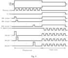
- the display scan clock signal Display_CLK as shown by the numeral 4 in Fig. 3 the DC signal VGH necessary for the display scan as shown by the numeral 5 in Fig. 3 , and the DC signal VGL as shown by the numeral 6 in Fig. 3 , are generated using the display scan control signal generation unit 301, and are output to the GOA unit 302.
- the first GOA unit 302 is driven to begin to perform the shift register, so that the individual GOA units 302 generate the display scan signals sequentially (assuming that the GOA unit 102 comprises X number of GOA units 302, and the display scan signals being Output'1 ⁇ Output'X), which are output to the corresponding gate lines 304 to complete the progressive scan for all the gate lines 304 in the GOA group 102.
- Tx CLK as shown by the numeral 1 in Fig. 3 and Tx_STV as shown by the numeral 2 in Fig. 3 generated by the drive line scan control signal generation unit 101 are applied to the GOA unit 302 involved in the drive line scan, so as to drive and control the GOA unit 302 to generate the output signal of the GOA unit (assuming that there are Y number of GOA units in the GOA unit 102 comprising X number of GOA units involved in the drive line scan, the output signals of the GOA units being GOA output'1 ⁇ GOA output'Y, as shown by the numeral 8 in Fig. 3 ).
- the drive line scan control signal generation unit 101 may be connected with the GOA unit 302 involved in the drive line scan through a diode, so as to ensure the unidirectional input of Tx_CLK and to prevent the short circuit between the GOA units 302. Further, a diode may be added between a pin for outputting Tx_STV in the drive line scan control signal generation unit 101 and the GOA unit 302 to ensure the unidirectional input of Tx_STV.
- the output signals of the GOA units may be connected through a diode to form the GOA group output signal, GOA output, as shown by the numeral 9 in Fig. 3 , as the GOA group input signal of the next GOA group 102.
- each of the output signals of the GOA units generated by the GOA units 302 involved in the drive line scan in the GOA group 102 is output to the corresponding drive line scan signal generation unit 303, so as to generate the drive line scan signals (i.e., Output'1 ⁇ Output'Y as shown by the numeral 10 in Fig.
- the drive line scan signal is output only at the drive line scan signal generation unit 303 connected with the GOA unit 302 involved in the drive line scan, and no drive line scan signal is output at the drive line scan signal generation unit 303 connected with the GOA unit 302 not involved in the drive line scan.
- the drive line scan signal is applied onto the corresponding gate line 304, so that the specific gate line may be scanned as the drive line.
- all the drive line scan signal generation units 303 connected with the GOA units 302 involved in the drive line scan generate Output'1 ⁇ Output'Y at the same time under the function of TX_Square wave and GOA output'1 ⁇ GOA output'Y
- all the gate lines 304 involved in the drive line scan are applied with Output'1 ⁇ Output'Y at the same time to complete the scan.
- Tx_STV is generated by the drive line scan control signal generation unit 101
- Display_STV is generated by the display scan control signal generation unit 301.
- Tx_STV and Display_STV may also be generated by the display scan control signal generation unit 301.
- Tx_CLK may exemplarily comprise a first drive line scan clock signal Tx_CLK1 as shown by the numeral 11 in Fig. 3 and a second drive line scan clock signal Tx_CLK2 as shown by the numeral 12 in Fig. 3 , in reverse phase with each other, so as to ensure a stable and accurate output of Tx_CLK.
- Display_CLK may exemplarily comprise a first display scan clock signal Display_CLK1 as shown by the numeral 41 in Fig. 3 and a second display scan clock signal Display_CLK2 as shown by the numeral 42 in Fig. 3 , in reverse phase with each other, so as to ensure a stable and accurate output of Display_CLK.
- Fig. 4 only shows the drive timings of Y number of GOA units 302 involved in the drive line scan in one GOA group 102 and the touch scan signal generation units 303 as well as the gate lines 304 connected with the Y number of GOA units 302.
- the drive timings of the (X-Y) number of GOA units 302 not involved in the drive line scan in the GOA group 102 and the touch scan signal generation units 303 as well as the gate lines 304 connected with the (X-Y) number of GOA units 302 are the same as those in the prior art in the display scan period, and are not operated in the touch scan period.
- the drive line scan signal generation unit 303 may exemplarily use an AND logic, and the drive line scan signal generation unit 303 may comprise an AND circuit, or comprise an NAND circuit and an NOT circuit. Additionally, the drive line scan signal generation unit 303 needs to be powered externally so as to operate normally, and the external voltage provided to the drive line scan signal generation unit 303 is determined according to different requirements in different periods.
- the voltage applied to the drive line scan signal generation module 103, which is applied to the drive line scan signal generation unit 303 actually, in the display scan period of one frame is larger than that in the touch scan period, so as to ensure that the pixels are charged normally in the display period and are turned off in the touch period, and that the drive line scan is performed for multiple gate lines 104.
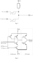
- the structure may be as shown in Fig. 5 exemplarily, in which the GOA output terminal is the input terminal to which the output signal of the GOA unit is input; the Tx_Square wave terminal is also the input terminal to which the drive line scan pulse signal is input, and the Output terminal is the output terminal from which the drive line scan signal is output.
- the GOA output terminal is connected with a diode M1 which may be exemplarily realized by an N-type TFT with the gate and the drain connected with each other.
- the Tx_Square wave terminal is connected with a diode M2 which may also be exemplarily realized by an N-type TFT with the gate and the drain connected with each other.
- a resistor R is connected at a common terminal of M1 and M2 and provides an offset voltage to the AND gate circuit through an external voltage VDD, which may be exemplarily realized by at least one TFT.
- the structure may be as shown in Fig. 6 exemplarily, in which the GOA output terminal is the input terminal to which the output signal of the GOA unit is input, the Tx_Square wave terminal is also the input terminal to which the drive line scan pulse signal is input, and the Output terminal is the output terminal from which the drive line scan signal is output;
- the NAND gate circuit is as shown in the slash box in the left, comprising four TFTs T1-T4 with the positive voltage being provided by VDD and the negative voltage being provided by VSS;
- the NOT gate circuit is as shown in the slash box in the right, which may be also referred to as an inverter circuit, comprising two TFTs T5 and T6.
- the high level is output at the Output terminal only when the high level is input to both the GOA output terminal and the Tx_Square wave terminal, and the low level is output at the Output terminal when any one or more than one of the GOA output terminal and the Tx_Square wave is at the low level.
- the GOA unit 302 is provided with the high level in a range of 10V ⁇ 30V for example, and the low level in a range of -8V ⁇ -12V for example, necessary for the normal charge, by VDD and VSS respectively, so as to turn on the TFT controlling the pixels to ensure that the pixels are charged.
- the values of VDD and VSS may be each determined depending on requirements and arc not necessarily within the above ranges.
- VDD and VSS may be decreased to about +3V and -3V respectively, for example, so as to ensure that the TFT controlling the pixels is turned off in the drive line scan of the normal touch drive.
- the values of VDD and VSS may be each determined depending on requirements and are not necessarily within the above ranges.
- the gate line group 104 comprises at least one gate line 304.
- the GOA circuit further comprises a TFT connected with the gate line 304, which is turned on under driven by the gate line 304 to charge the corresponding pixel.
- the GOA circuit in the present embodiment can realize a time division multiplexing for the gate lines 304.
- the gate line when taken as the drive line of the touch signal in the touch scan period, it requires a large voltage, generally between 3V-5V, which may cause the TFT controlling the charge to the pixels to generate a relatively large leak current, affecting the actual voltage of the pixel and thus affecting the display effect of the image.
- the threshold voltage of the TFT may be the voltage necessary to be applied when the gate line is taken as the drive line for the touch drive, so that when the scan is performed for the gate line in the touch scan period, the TFT with the high threshold voltage is always in a turned off state, the leak current is very small, and the touch scan operation is completed with little effect on the pixel voltage.
- the high threshold voltage of the TFT may be realized by changing the thickness and the material of the gate insulation layer, a doping process adjustment, or the like.
- the gate insulation layer may be manufactured by, for example, a silicon oxide material, in a plasma chemical vapor deposition process, so that the threshold voltage of the TFT may be about 10V.
- the TFT array substrate which has been manufactured is subject to an annealing process, with the annealing temperature between 280°C ⁇ 300°C and the annealing time being 1 hour, so that the threshold voltage of the TFT may be decreased to about 3 V ⁇ 5 V.
- the TFT controlling the charge to the pixels in the present embodiment may be exemplarily an oxide TFT.
- the oxide TFT has a smaller sub threshold amplitude, a faster operation speed in the sub threshold region, and may make the leak current change substantially without increasing the turn on voltage of the TFT substantially.
- the elements in the GOA circuit provided in the present embodiment may use various types of TFTs, such as a Low Temperature Poly-Silicon, a monosilicon, an oxide TFT or the like, so as to simplify the manufacture process of the circuit and meanwhile optimize the circuit performance.
- TFTs such as a Low Temperature Poly-Silicon, a monosilicon, an oxide TFT or the like
- the realization of the drive line scan in the touch scan is mainly described in the present embodiment in detail.
- the sensing line scan in the touch drive may be realized in a way of a common electrode, a common data line, a sensing line made individually, or the like.
- a display apparatus is further provided in the present embodiment, which comprises the GOA circuit described in the present embodiment.
- the GOA circuit provided in the present embodiment may perform the time division multiplexing for the gate lines to realize the integration of display scan and touch scan functions and save the area of the control chip, it is helpful in making the display apparatus thinner and lighter.
- the complexity of the control chip circuit is decreased, the cost of the control chip may be decreased, and the entire manufacture cost of the display apparatus may be decreased.
- the touch scan function is integrated into the GOA circuit so that the peripheral wirings of the display panel is decreased, which is helpful in realizing a display apparatus with a narrow frame. Meanwhile, the touch scan function is integrated into the GOA circuit, which is helpful in decreasing the signal delay and decreasing the power consumption of the apparatus.
- the type of display apparatus to which the GOA circuit is applied is not limited in the present embodiment, and may be a liquid crystal display apparatus, an organic light emitting diode display apparatus, or the like.
Landscapes
- Engineering & Computer Science (AREA)
- Theoretical Computer Science (AREA)
- General Engineering & Computer Science (AREA)
- Physics & Mathematics (AREA)
- General Physics & Mathematics (AREA)
- Human Computer Interaction (AREA)
- Computer Networks & Wireless Communication (AREA)
- Computer Hardware Design (AREA)
- Liquid Crystal Display Device Control (AREA)
- Control Of Indicators Other Than Cathode Ray Tubes (AREA)
- Chemical & Material Sciences (AREA)
- Crystallography & Structural Chemistry (AREA)
Claims (10)
- Eine Gate Driver on Array (GOA)Schaltung, umfassend:eine Ansteuerungsleitungsabtaststeuerungssignalerzeugungseinheit (101), die so konfiguriert ist, dass sie ein Ansteuerungsleitungsabtasttaktsignal und ein Ansteuerungsleitungsabtastpulssignal erzeugt;mehrere GOA-Gruppen (102), die mit der Ansteuerungsleitungsabtaststeuerungssignalerzeugungseinheit (101) verbunden und sequentiell miteinander in Reihe geschaltet sind, die konfiguriert sind, dass sie das Ansteuerungsleitungsabtasttaktsignal erfassen, um GOA-Gruppen-Ausgangssignale sequentiell entsprechend den GOA-Gruppen-Eingangssignalen zu erzeugen, wobei das mittels einer der GOA-Gruppen erzeugte GOA-Gruppen-Ausgangssignal das GOA-Gruppen-Eingangssignal einer nächsten GOA-Gruppe ist, um eine Schieberegisterfunktion der mehreren GOA-Gruppen zu realisieren;mehrere Ansteuerungsleitungsabtastsignalerzeugungsgruppen (103), die jeweils mit den mehreren GOA-Gruppen (102) verbunden sind und mit der Ansteuerungsleitungsabtaststeuerungssignalerzeugungseinheit (101) verbunden sind, die konfiguriert sind, dass sie die GOA-Gruppenausgangssignale und das Ansteuerungsleitungsabtastpulssignal erfassen und dass sie nacheinander Ansteuerungsleitungsabtastsignale erzeugen;mehrere Gate-Leitungsgruppen (104), die jeweils mit den mehreren Ansteuerungsleitungsabtastsignalerzeugungsgruppen (103) verbunden sind, die konfiguriert sind, dass sie mit den Ansteuerungsleitungsabtastsignalen beaufschlagt werden, um die Ansteuerungsleitungsabtastung für die mehreren Gate-Leitungsgruppen nacheinander zu vervollständigen,dadurch gekennzeichnet:dass eine an die Ansteuerungsleitungsabtastsignalerzeugungsgruppe (103) in einer Anzeigeabtastperiode eines Bildes angelegte Spannung größer ist als die an die Ansteuerungsleitungsabtastsignalerzeugungsgruppe (103) in einer Berührungsabtastperiode angelegte Spannung,wobei die Gate-Leitungsgruppe (104) mindestens eine Gate-Leitung (304) umfasst, und die GOA-Schaltung ferner umfasst: einen Dünnfilmtransistor (TFT), der mit der Gate-Leitung (304) verbunden ist, wobei eine Schwellenspannung des TFT eine Spannung ist, die angelegt werden muss, wenn die Gate-Leitung als eine Ansteuerungsleitung für Berührungsansteuerung genommen wird, und der TFT ein Oxid-TFT ist,wobei jede der mehreren GOA-Gruppen (102) die gleiche Anzahl von mehreren GOA-Einheiten (302) umfasst, die Ansteuerungsleitungsabtastsignalerzeugungsgruppe (103) die gleiche Anzahl von mehreren Ansteuerungsleitungsabtastsignalerzeugungseinheiten (303) umfasst, die Gate-Leitungsgruppe (104) die gleiche Anzahl von mehreren Gate-Leitungen (304) umfasst, die Anzahlen von GOA-Einheiten (302), die an der Ansteuerungsleitungsabtastung in jeder GOA-Gruppe (102) beteiligt sind, die gleichen sind und eine Mehrzahl sind;wobei mindestens eine GOA-Einheit (302) in jeder GOA-Gruppe (102) mit der Ansteuerungsleitungsabtaststeuerungssignalerzeugungseinheit (101) verbunden ist, um in die Ansteuerungsleitungsabtastung involviert zu sein, jede der GOA-Einheiten (302), die in die Ansteuerungsleitungsabtastung involviert sind, über eine der Ansteuerungsleitungsabtastsignalerzeugungseinheiten (303) mit einer der Gate-Leitungen (304) verbunden ist;wobei zwei benachbarte GOA-Einheiten (302), die an der Ansteuerungsleitungsabtastung in jeder der mehreren GOA-Gruppen (102) involviert sind, mittels mindestens einer GOA-Einheit (302), die nicht in Ansteuerungsleitungsabtastung involviert ist, beabstandet sind, um die Schieberegisterfunktion zwischen der GOA-Einheit (302), die in die Ansteuerungsleitungsabtastung involviert ist, und der GOA-Einheit (302), die nicht in die Ansteuerungsleitungsabtastung involviert ist, zu unterbrechen.
- GOA-Schaltung gemäß Anspruch 1, wobei
die Ausgangssignale der GOA-Einheiten (302), die in die Ansteuerungsleitungsabtastung in einer der GOA-Gruppen (102) involviert sind, durch eine Diode verbunden sind, um das GOA-Gruppen-Ausgangssignal als GOA-Gruppen-Eingangssignal für die nächste GOA-Gruppe (102) zu bilden. - GOA-Schaltung gemäß Anspruch 2, wobei die Anzahl der GOA-Einheiten (302), die nicht in die Ansteuerungsleitungsabtastung involviert sind, die zwischen zwei benachbarten GOA-Einheiten (302), die in die Ansteuerungsleitungsabtastung involviert sind, beabstandet sind, gleich ist.
- GOA-Schaltung gemäß Anspruch 1, bei der alle GOA-Einheiten (302) in jeder der mehreren GOA-Gruppen (102) mit einer der Gate-Leitungen (304) durch eine der Ansteuerungsleitungsabtastsignalerzeugungseinheiten (303) verbunden sind.
- GOA-Schaltung gemäß einem der Ansprüche 1 bis 4, wobei die Ansteuerungsleitungsabtaststeuerungssignalerzeugungseinheit (101) mit der GOA-Einheit (302), die in die Ansteuerungsleitungsabtastung involviert ist, durch eine Diode verbunden ist, um eine unidirektionale Eingabe des Ansteuerungsleitungsabtastsignals sicherzustellen und einen Kurzschluss zwischen den GOA-Einheiten (302) zu verhindern.
- GOA-Schaltung gemäß einem der Ansprüche 1 bis 5, wobei die Ansteuerungsleitungsabtastsignalerzeugungseinheit (303) eine UND-Gate-Schaltung umfasst oder die Ansteuerungsleitungsabtastsignalerzeugungseinheit (303) eine NAND-Gate-Schaltung und eine NICHT-Gate-Schaltung umfasst.
- GOA-Schaltung gemäß einem der Ansprüche 1 bis 6, wobei ein Taktzyklus des Ansteuerungsleitungsabtasttaktsignals als Zeit festgelegt wird, die für die Vervollständigung der Abtastung einer Ansteuerungsleitung erforderlich ist;
eine Impulsbreite des Ansteuerungsleitungsabtastpulssignal als eine Pulsbreite gesetzt wird, die für die Durchführung einer Berührungsabtastung erforderlich ist. - GOA-Schaltung gemäß einem der Ansprüche 1 bis 7, wobei das Ansteuerungsleitungsabtasttaktsignal ein erstes Ansteuerungsleitungsabtasttaktsignal und ein zweites Ansteuerungsleitungsabtasttaktsignal mit umgekehrten Phasen enthält.
- Die GOA-Schaltung gemäß einem der Ansprüche 1 bis 8, wobei die Ansteuerungsleitungsabtaststeuerungssignalerzeugungseinheit (101) ferner konfiguriert ist, dass sie ein originales Eingangssignal für die Ansteuerungsleitungsabtastung als GOA-Gruppeneingangssignal für die erste GOA-Gruppe (102) erzeugt.
- Anzeigegerät mit der GOA-Schaltung gemäß einem der Ansprüche 1-9.
Applications Claiming Priority (2)
| Application Number | Priority Date | Filing Date | Title |
|---|---|---|---|
| CN201410406028.5A CN104240631B (zh) | 2014-08-18 | 2014-08-18 | Goa电路及其驱动方法、显示装置 |
| PCT/CN2014/089586 WO2016026209A1 (zh) | 2014-08-18 | 2014-10-27 | Goa电路及其驱动方法、显示装置 |
Publications (3)
| Publication Number | Publication Date |
|---|---|
| EP3185236A1 EP3185236A1 (de) | 2017-06-28 |
| EP3185236A4 EP3185236A4 (de) | 2018-04-04 |
| EP3185236B1 true EP3185236B1 (de) | 2023-07-26 |
Family
ID=52228609
Family Applications (1)
| Application Number | Title | Priority Date | Filing Date |
|---|---|---|---|
| EP14884262.8A Active EP3185236B1 (de) | 2014-08-18 | 2014-10-27 | Goa-schaltung und ansteuerungsverfahren dafür sowie anzeigevorrichtung |
Country Status (4)
| Country | Link |
|---|---|
| US (1) | US9626028B2 (de) |
| EP (1) | EP3185236B1 (de) |
| CN (1) | CN104240631B (de) |
| WO (1) | WO2016026209A1 (de) |
Families Citing this family (55)
| Publication number | Priority date | Publication date | Assignee | Title |
|---|---|---|---|---|
| US9727162B2 (en) * | 2014-12-30 | 2017-08-08 | Shenzhen China Star Optoelectronics Technology Co., Ltd | GOA driving circuit applied for flat panel display device and flat panel display device |
| CN104537994B (zh) * | 2014-12-30 | 2017-04-12 | 深圳市华星光电技术有限公司 | 一种应用于平板显示器的goa驱动电路及平板显示器 |
| CN104485082B (zh) * | 2014-12-31 | 2017-02-22 | 厦门天马微电子有限公司 | 一种阵列基板和触控显示装置及其驱动方法 |
| CN104485080B (zh) * | 2014-12-31 | 2017-02-22 | 深圳市华星光电技术有限公司 | 用于液晶显示装置的goa电路 |
| CN104700766B (zh) * | 2015-03-31 | 2017-12-15 | 京东方科技集团股份有限公司 | 控制子单元、移位寄存单元、移位寄存器和显示装置 |
| CN104699315B (zh) | 2015-04-01 | 2018-03-13 | 上海天马微电子有限公司 | 一种触控面板、触控显示面板和显示装置 |
| CN104849889B (zh) * | 2015-05-12 | 2018-05-18 | 深圳市华星光电技术有限公司 | 液晶显示面板及液晶显示装置 |
| CN104916243B (zh) * | 2015-06-29 | 2017-10-17 | 深圳市华星光电技术有限公司 | 扫描驱动电路的检测方法和检测装置、液晶面板 |
| CN104916251B (zh) * | 2015-07-10 | 2018-09-28 | 京东方科技集团股份有限公司 | 栅极驱动电路、触控显示装置和触控显示驱动方法 |
| CN105261320B (zh) * | 2015-07-22 | 2018-11-30 | 京东方科技集团股份有限公司 | Goa单元驱动电路及其驱动方法、显示面板及显示装置 |
| CN105096874B (zh) * | 2015-08-12 | 2017-10-17 | 武汉华星光电技术有限公司 | 一种 goa 电路、阵列基板和液晶显示器 |
| US10809855B2 (en) * | 2015-08-19 | 2020-10-20 | Novatek Microelectronics Corp. | Driving circuit and a method for driving a display panel having a touch panel |
| CN105118431A (zh) * | 2015-08-31 | 2015-12-02 | 上海和辉光电有限公司 | 像素驱动电路及其驱动方法和显示装置 |
| CN105183233B (zh) * | 2015-09-24 | 2018-02-23 | 深圳市华星光电技术有限公司 | 触控屏以及智能终端 |
| TWI576738B (zh) * | 2015-11-04 | 2017-04-01 | 友達光電股份有限公司 | 移位暫存器 |
| CN105244005B (zh) | 2015-11-24 | 2018-01-09 | 厦门天马微电子有限公司 | 阵列基板、触控显示装置及其驱动方法 |
| CN105374331B (zh) * | 2015-12-01 | 2017-11-17 | 武汉华星光电技术有限公司 | 栅极驱动电路和使用栅极驱动电路的显示器 |
| CN105679248B (zh) * | 2016-01-04 | 2017-12-08 | 京东方科技集团股份有限公司 | 移位寄存器单元及其驱动方法、栅极驱动电路、显示装置 |
| CN105448227B (zh) * | 2016-01-12 | 2017-11-17 | 京东方科技集团股份有限公司 | 一种栅极驱动电路和显示装置 |
| CN105448226B (zh) * | 2016-01-12 | 2018-03-16 | 京东方科技集团股份有限公司 | 一种栅极驱动电路和显示装置 |
| CN105528984A (zh) | 2016-02-02 | 2016-04-27 | 京东方科技集团股份有限公司 | 发射电极扫描驱动单元、驱动电路以及驱动方法、阵列基板 |
| CN105528118B (zh) * | 2016-02-17 | 2018-05-18 | 京东方科技集团股份有限公司 | 触控显示面板及其驱动方法、感应信号的侦测方法 |
| CN105549289B (zh) * | 2016-03-09 | 2018-12-21 | 武汉华星光电技术有限公司 | 一种阵列基板、显示器和测试系统 |
| CN105788557B (zh) * | 2016-05-20 | 2018-06-19 | 武汉华星光电技术有限公司 | Goa驱动电路 |
| CN106097997A (zh) * | 2016-06-14 | 2016-11-09 | 武汉华星光电技术有限公司 | In‑Cell触控显示面板的驱动方法及驱动电路 |
| CN106205521B (zh) * | 2016-07-08 | 2018-10-23 | 武汉华星光电技术有限公司 | 一种显示面板的驱动方法及驱动装置 |
| CN106205558B (zh) * | 2016-09-30 | 2018-09-21 | 京东方科技集团股份有限公司 | 像素驱动方法及装置 |
| KR102703113B1 (ko) * | 2016-10-20 | 2024-09-05 | 주식회사 엘엑스세미콘 | 인셀 터치 유기발광표시장치 및 그 구동회로 |
| CN106569650B (zh) * | 2016-11-02 | 2020-03-10 | 武汉华星光电技术有限公司 | 一种触摸面板及显示装置 |
| CN108109592B (zh) * | 2016-11-25 | 2022-01-25 | 株式会社半导体能源研究所 | 显示装置及其工作方法 |
| CN106652883B (zh) * | 2017-03-21 | 2020-04-28 | 上海中航光电子有限公司 | 一种栅极驱动电路 |
| CN108806571B (zh) | 2017-05-04 | 2021-09-21 | 京东方科技集团股份有限公司 | 栅极驱动电路及其驱动方法、阵列基板及显示装置 |
| TWI643172B (zh) * | 2017-11-01 | 2018-12-01 | 元太科技工業股份有限公司 | 顯示面板的驅動方法 |
| CN109754758B (zh) | 2017-11-01 | 2020-11-03 | 元太科技工业股份有限公司 | 显示面板的驱动方法 |
| CN108172162A (zh) * | 2018-01-02 | 2018-06-15 | 京东方科技集团股份有限公司 | 一种阵列基板驱动方法、驱动装置及显示装置 |
| CN107967907B (zh) * | 2018-01-18 | 2021-03-09 | 京东方科技集团股份有限公司 | 反相电路、驱动方法、阵列基板、检测方法及显示装置 |
| CN108447453B (zh) * | 2018-04-10 | 2021-04-23 | 京东方科技集团股份有限公司 | Goa电路及其驱动方法、触控显示装置 |
| CN108766335B (zh) | 2018-05-23 | 2020-06-16 | 京东方科技集团股份有限公司 | Goa单元、goa电路、显示装置及栅极驱动方法 |
| CN109064986B (zh) * | 2018-08-29 | 2021-01-26 | 京东方科技集团股份有限公司 | 一种显示面板及其制作方法、驱动方法、显示装置 |
| CN108877662B (zh) * | 2018-09-13 | 2020-03-31 | 合肥鑫晟光电科技有限公司 | 栅极驱动电路及其控制方法、显示装置 |
| CN109147630A (zh) * | 2018-09-25 | 2019-01-04 | 武汉华星光电半导体显示技术有限公司 | 一种goa检测电路及其测试方法 |
| CN109698006B (zh) | 2019-02-19 | 2021-01-26 | 京东方科技集团股份有限公司 | 移位寄存器及其驱动方法、级联驱动电路和显示装置 |
| WO2020168491A1 (zh) * | 2019-02-20 | 2020-08-27 | 京东方科技集团股份有限公司 | 移位寄存电路、驱动电路、显示装置及驱动方法 |
| CN109767716B (zh) * | 2019-03-12 | 2022-09-06 | 京东方科技集团股份有限公司 | 一种阵列基板、显示装置及驱动方法 |
| CN110060639B (zh) * | 2019-04-24 | 2021-07-06 | 深圳市华星光电半导体显示技术有限公司 | 阵列基板 |
| CN110728940B (zh) * | 2019-09-17 | 2020-12-08 | 深圳市华星光电半导体显示技术有限公司 | 反相器、goa电路及显示面板 |
| CN110800039B (zh) | 2019-09-17 | 2021-10-08 | 京东方科技集团股份有限公司 | Goa单元电路、驱动方法、goa电路和显示装置 |
| KR102137638B1 (ko) * | 2020-01-15 | 2020-07-27 | 주식회사 사피엔반도체 | 디스플레이 패널의 보다 세분화된 밝기 제어가 가능한 디스플레이 장치 |
| CN111613182A (zh) * | 2020-05-25 | 2020-09-01 | 武汉华星光电半导体显示技术有限公司 | 显示面板及其驱动方法、电子设备 |
| CN112037729A (zh) * | 2020-09-23 | 2020-12-04 | 京东方科技集团股份有限公司 | 显示面板控制方法及装置、显示面板及电子设备 |
| CN112489594B (zh) * | 2020-12-11 | 2022-12-20 | 武汉天马微电子有限公司 | 一种扫描信号控制电路的控制方法及控制电路、显示装置 |
| CN113920946B (zh) * | 2021-10-18 | 2023-02-28 | 京东方科技集团股份有限公司 | 栅极驱动器及其驱动方法、显示装置 |
| CN114724526B (zh) * | 2022-06-07 | 2022-09-27 | 惠科股份有限公司 | 栅极驱动电路、显示面板及显示装置 |
| CN117289818A (zh) * | 2023-08-25 | 2023-12-26 | 湖北长江新型显示产业创新中心有限公司 | 扫描信号驱动电路、显示面板、显示装置及驱动方法 |
| CN117276292B (zh) * | 2023-11-21 | 2024-04-23 | 惠科股份有限公司 | 阵列基板及显示面板 |
Citations (1)
| Publication number | Priority date | Publication date | Assignee | Title |
|---|---|---|---|---|
| CN103258514A (zh) * | 2013-05-06 | 2013-08-21 | 深圳市华星光电技术有限公司 | Goa驱动电路及驱动方法 |
Family Cites Families (24)
| Publication number | Priority date | Publication date | Assignee | Title |
|---|---|---|---|---|
| JPH0879663A (ja) * | 1994-09-07 | 1996-03-22 | Sharp Corp | 駆動回路及び表示装置 |
| JP3832439B2 (ja) * | 2003-02-19 | 2006-10-11 | ソニー株式会社 | 表示装置およびその駆動方法 |
| JP2006285141A (ja) * | 2005-04-05 | 2006-10-19 | Mitsubishi Electric Corp | マトリックス表示装置 |
| JP5128102B2 (ja) * | 2006-02-23 | 2013-01-23 | 三菱電機株式会社 | シフトレジスタ回路およびそれを備える画像表示装置 |
| CN101634917B (zh) * | 2008-07-21 | 2013-04-24 | 智点科技(深圳)有限公司 | 一种触控式平板显示器 |
| CN101762915B (zh) | 2008-12-24 | 2013-04-17 | 北京京东方光电科技有限公司 | Tft-lcd阵列基板及其驱动方法 |
| JP5670124B2 (ja) * | 2010-08-23 | 2015-02-18 | 株式会社ジャパンディスプレイ | タッチ検出機能付き表示装置、駆動回路、タッチ検出機能付き表示装置の駆動方法および電子機器 |
| JP5424347B2 (ja) * | 2010-09-17 | 2014-02-26 | 株式会社ジャパンディスプレイ | タッチ検出機能付き表示装置およびその駆動方法、駆動回路、ならびに電子機器 |
| TWI439050B (zh) * | 2010-10-27 | 2014-05-21 | Au Optronics Corp | 移位暫存器及觸控裝置 |
| WO2012147637A1 (ja) * | 2011-04-28 | 2012-11-01 | シャープ株式会社 | 液晶表示装置 |
| US9317151B2 (en) * | 2012-05-14 | 2016-04-19 | Apple Inc. | Low complexity gate line driver circuitry |
| JP6055206B2 (ja) * | 2012-06-08 | 2016-12-27 | 株式会社ジャパンディスプレイ | 液晶表示装置 |
| TW201351225A (zh) * | 2012-06-11 | 2013-12-16 | Giantplus Technology Co Ltd | 內嵌式觸控顯示器電路結構 |
| CN107291304B (zh) * | 2012-06-28 | 2021-08-24 | 上海天马微电子有限公司 | 触摸显示屏的驱动方法 |
| CN102750062B (zh) * | 2012-06-29 | 2016-02-10 | 京东方科技集团股份有限公司 | 一种电容式内嵌触摸屏及显示装置 |
| US20140002410A1 (en) * | 2012-06-29 | 2014-01-02 | Synaptics Incorporated | Fully addressable transmitter electrode control |
| KR101628724B1 (ko) * | 2012-11-13 | 2016-06-09 | 엘지디스플레이 주식회사 | 터치스크린 일체형 표시장치 |
| KR101606874B1 (ko) * | 2012-12-28 | 2016-03-28 | 엘지디스플레이 주식회사 | 터치스크린 일체형 표시장치 및 그 구동 방법 |
| US20140225840A1 (en) * | 2013-02-14 | 2014-08-14 | Apple Inc. | Touchscreen system having on-panel touch driver circuitry |
| CN103412672A (zh) * | 2013-07-17 | 2013-11-27 | 北京京东方光电科技有限公司 | 一种触控显示装置及其驱动方法 |
| CN103823589B (zh) * | 2014-01-24 | 2017-03-15 | 京东方科技集团股份有限公司 | 一种触摸电路及驱动方法、触摸显示装置 |
| CN103913915B (zh) * | 2014-03-27 | 2016-08-17 | 京东方科技集团股份有限公司 | 一种阵列基板、显示面板和显示装置 |
| CN103943083B (zh) * | 2014-03-27 | 2017-02-15 | 京东方科技集团股份有限公司 | 一种栅极驱动电路及其驱动方法、显示装置 |
| CN103943055B (zh) * | 2014-03-27 | 2016-05-11 | 京东方科技集团股份有限公司 | 一种栅极驱动电路及其驱动方法、显示装置 |
-
2014
- 2014-08-18 CN CN201410406028.5A patent/CN104240631B/zh active Active
- 2014-10-27 EP EP14884262.8A patent/EP3185236B1/de active Active
- 2014-10-27 US US14/772,638 patent/US9626028B2/en active Active
- 2014-10-27 WO PCT/CN2014/089586 patent/WO2016026209A1/zh not_active Ceased
Patent Citations (2)
| Publication number | Priority date | Publication date | Assignee | Title |
|---|---|---|---|---|
| CN103258514A (zh) * | 2013-05-06 | 2013-08-21 | 深圳市华星光电技术有限公司 | Goa驱动电路及驱动方法 |
| US20150154927A1 (en) * | 2013-05-06 | 2015-06-04 | Shenzhen China Star Optoelectronics Technology Co., Ltd. | Gate driver-on-array driving circuit and driving method |
Also Published As
| Publication number | Publication date |
|---|---|
| EP3185236A4 (de) | 2018-04-04 |
| US9626028B2 (en) | 2017-04-18 |
| CN104240631B (zh) | 2016-09-28 |
| WO2016026209A1 (zh) | 2016-02-25 |
| US20160259455A1 (en) | 2016-09-08 |
| CN104240631A (zh) | 2014-12-24 |
| EP3185236A1 (de) | 2017-06-28 |
Similar Documents
| Publication | Publication Date | Title |
|---|---|---|
| EP3185236B1 (de) | Goa-schaltung und ansteuerungsverfahren dafür sowie anzeigevorrichtung | |
| US9733759B2 (en) | Driving circuit, array substrate, touch display device, and driving method of the touch display device | |
| EP3200179B1 (de) | Gate-treiber, anzeigevorrichtung und gate-ansteuerungsverfahren | |
| US9733758B2 (en) | Array substrate, touch display device, and driving method of the touch display device | |
| KR102381885B1 (ko) | 디스플레이 장치 | |
| US9946349B2 (en) | Shift register, driving method, gate driving circuit and display device | |
| US9875708B2 (en) | Driving circuit, array substrate and display apparatus | |
| US10665186B2 (en) | Display apparatus | |
| US10490133B2 (en) | Shift register module and display driving circuit thereof | |
| US9317151B2 (en) | Low complexity gate line driver circuitry | |
| EP3882901B1 (de) | Schieberegistereinheit und antriebsverfahren, gate-treiberschaltung und anzeigevorrichtung | |
| US11662865B2 (en) | Array substrate and driving method, display panel and touch display device | |
| US9880662B2 (en) | Touch driving unit and circuit, display panel and display device | |
| KR20160081702A (ko) | 데이터 제어회로 및 이를 포함하는 평판표시장치 | |
| CN107871480B (zh) | 栅极驱动电路、电平移位器和显示装置 | |
| US10115364B2 (en) | Scanning device circuits and flat display devices having the same | |
| TW202117522A (zh) | 觸控顯示驅動電路、觸控顯示裝置以及觸控顯示驅動方法 | |
| WO2017012255A1 (zh) | Goa单元驱动电路及其驱动方法、显示面板及显示装置 | |
| WO2016074357A1 (zh) | 内嵌式触摸屏及其驱动方法和显示装置 | |
| CN111971736B (zh) | 移位寄存器、其驱动方法及装置 | |
| KR102381628B1 (ko) | 디스플레이 장치 | |
| CN205177380U (zh) | 一种移位寄存单元、触控显示面板及触控显示装置 |
Legal Events
| Date | Code | Title | Description |
|---|---|---|---|
| PUAI | Public reference made under article 153(3) epc to a published international application that has entered the european phase |
Free format text: ORIGINAL CODE: 0009012 |
|
| STAA | Information on the status of an ep patent application or granted ep patent |
Free format text: STATUS: REQUEST FOR EXAMINATION WAS MADE |
|
| 17P | Request for examination filed |
Effective date: 20150908 |
|
| AK | Designated contracting states |
Kind code of ref document: A1 Designated state(s): AL AT BE BG CH CY CZ DE DK EE ES FI FR GB GR HR HU IE IS IT LI LT LU LV MC MK MT NL NO PL PT RO RS SE SI SK SM TR |
|
| AX | Request for extension of the european patent |
Extension state: BA ME |
|
| DAX | Request for extension of the european patent (deleted) | ||
| A4 | Supplementary search report drawn up and despatched |
Effective date: 20180306 |
|
| RIC1 | Information provided on ipc code assigned before grant |
Ipc: G09G 3/32 20160101ALI20180228BHEP Ipc: G09G 3/20 20060101AFI20180228BHEP |
|
| STAA | Information on the status of an ep patent application or granted ep patent |
Free format text: STATUS: EXAMINATION IS IN PROGRESS |
|
| 17Q | First examination report despatched |
Effective date: 20201005 |
|
| GRAP | Despatch of communication of intention to grant a patent |
Free format text: ORIGINAL CODE: EPIDOSNIGR1 |
|
| STAA | Information on the status of an ep patent application or granted ep patent |
Free format text: STATUS: GRANT OF PATENT IS INTENDED |
|
| INTG | Intention to grant announced |
Effective date: 20230227 |
|
| GRAS | Grant fee paid |
Free format text: ORIGINAL CODE: EPIDOSNIGR3 |
|
| GRAA | (expected) grant |
Free format text: ORIGINAL CODE: 0009210 |
|
| STAA | Information on the status of an ep patent application or granted ep patent |
Free format text: STATUS: THE PATENT HAS BEEN GRANTED |
|
| AK | Designated contracting states |
Kind code of ref document: B1 Designated state(s): AL AT BE BG CH CY CZ DE DK EE ES FI FR GB GR HR HU IE IS IT LI LT LU LV MC MK MT NL NO PL PT RO RS SE SI SK SM TR |
|
| REG | Reference to a national code |
Ref country code: CH Ref legal event code: EP |
|
| REG | Reference to a national code |
Ref country code: IE Ref legal event code: FG4D |
|
| REG | Reference to a national code |
Ref country code: DE Ref legal event code: R096 Ref document number: 602014087781 Country of ref document: DE |
|
| REG | Reference to a national code |
Ref country code: LT Ref legal event code: MG9D |
|
| REG | Reference to a national code |
Ref country code: NL Ref legal event code: MP Effective date: 20230726 |
|
| REG | Reference to a national code |
Ref country code: AT Ref legal event code: MK05 Ref document number: 1592870 Country of ref document: AT Kind code of ref document: T Effective date: 20230726 |
|
| PG25 | Lapsed in a contracting state [announced via postgrant information from national office to epo] |
Ref country code: NL Free format text: LAPSE BECAUSE OF FAILURE TO SUBMIT A TRANSLATION OF THE DESCRIPTION OR TO PAY THE FEE WITHIN THE PRESCRIBED TIME-LIMIT Effective date: 20230726 |
|
| PG25 | Lapsed in a contracting state [announced via postgrant information from national office to epo] |
Ref country code: GR Free format text: LAPSE BECAUSE OF FAILURE TO SUBMIT A TRANSLATION OF THE DESCRIPTION OR TO PAY THE FEE WITHIN THE PRESCRIBED TIME-LIMIT Effective date: 20231027 |
|
| PG25 | Lapsed in a contracting state [announced via postgrant information from national office to epo] |
Ref country code: IS Free format text: LAPSE BECAUSE OF FAILURE TO SUBMIT A TRANSLATION OF THE DESCRIPTION OR TO PAY THE FEE WITHIN THE PRESCRIBED TIME-LIMIT Effective date: 20231126 |
|
| PG25 | Lapsed in a contracting state [announced via postgrant information from national office to epo] |
Ref country code: SE Free format text: LAPSE BECAUSE OF FAILURE TO SUBMIT A TRANSLATION OF THE DESCRIPTION OR TO PAY THE FEE WITHIN THE PRESCRIBED TIME-LIMIT Effective date: 20230726 Ref country code: RS Free format text: LAPSE BECAUSE OF FAILURE TO SUBMIT A TRANSLATION OF THE DESCRIPTION OR TO PAY THE FEE WITHIN THE PRESCRIBED TIME-LIMIT Effective date: 20230726 Ref country code: PT Free format text: LAPSE BECAUSE OF FAILURE TO SUBMIT A TRANSLATION OF THE DESCRIPTION OR TO PAY THE FEE WITHIN THE PRESCRIBED TIME-LIMIT Effective date: 20231127 Ref country code: NO Free format text: LAPSE BECAUSE OF FAILURE TO SUBMIT A TRANSLATION OF THE DESCRIPTION OR TO PAY THE FEE WITHIN THE PRESCRIBED TIME-LIMIT Effective date: 20231026 Ref country code: LV Free format text: LAPSE BECAUSE OF FAILURE TO SUBMIT A TRANSLATION OF THE DESCRIPTION OR TO PAY THE FEE WITHIN THE PRESCRIBED TIME-LIMIT Effective date: 20230726 Ref country code: LT Free format text: LAPSE BECAUSE OF FAILURE TO SUBMIT A TRANSLATION OF THE DESCRIPTION OR TO PAY THE FEE WITHIN THE PRESCRIBED TIME-LIMIT Effective date: 20230726 Ref country code: IS Free format text: LAPSE BECAUSE OF FAILURE TO SUBMIT A TRANSLATION OF THE DESCRIPTION OR TO PAY THE FEE WITHIN THE PRESCRIBED TIME-LIMIT Effective date: 20231126 Ref country code: HR Free format text: LAPSE BECAUSE OF FAILURE TO SUBMIT A TRANSLATION OF THE DESCRIPTION OR TO PAY THE FEE WITHIN THE PRESCRIBED TIME-LIMIT Effective date: 20230726 Ref country code: GR Free format text: LAPSE BECAUSE OF FAILURE TO SUBMIT A TRANSLATION OF THE DESCRIPTION OR TO PAY THE FEE WITHIN THE PRESCRIBED TIME-LIMIT Effective date: 20231027 Ref country code: FI Free format text: LAPSE BECAUSE OF FAILURE TO SUBMIT A TRANSLATION OF THE DESCRIPTION OR TO PAY THE FEE WITHIN THE PRESCRIBED TIME-LIMIT Effective date: 20230726 Ref country code: AT Free format text: LAPSE BECAUSE OF FAILURE TO SUBMIT A TRANSLATION OF THE DESCRIPTION OR TO PAY THE FEE WITHIN THE PRESCRIBED TIME-LIMIT Effective date: 20230726 |
|
| PG25 | Lapsed in a contracting state [announced via postgrant information from national office to epo] |
Ref country code: PL Free format text: LAPSE BECAUSE OF FAILURE TO SUBMIT A TRANSLATION OF THE DESCRIPTION OR TO PAY THE FEE WITHIN THE PRESCRIBED TIME-LIMIT Effective date: 20230726 |
|
| PG25 | Lapsed in a contracting state [announced via postgrant information from national office to epo] |
Ref country code: ES Free format text: LAPSE BECAUSE OF FAILURE TO SUBMIT A TRANSLATION OF THE DESCRIPTION OR TO PAY THE FEE WITHIN THE PRESCRIBED TIME-LIMIT Effective date: 20230726 |
|
| REG | Reference to a national code |
Ref country code: DE Ref legal event code: R097 Ref document number: 602014087781 Country of ref document: DE |
|
| PG25 | Lapsed in a contracting state [announced via postgrant information from national office to epo] |
Ref country code: SM Free format text: LAPSE BECAUSE OF FAILURE TO SUBMIT A TRANSLATION OF THE DESCRIPTION OR TO PAY THE FEE WITHIN THE PRESCRIBED TIME-LIMIT Effective date: 20230726 Ref country code: RO Free format text: LAPSE BECAUSE OF FAILURE TO SUBMIT A TRANSLATION OF THE DESCRIPTION OR TO PAY THE FEE WITHIN THE PRESCRIBED TIME-LIMIT Effective date: 20230726 Ref country code: ES Free format text: LAPSE BECAUSE OF FAILURE TO SUBMIT A TRANSLATION OF THE DESCRIPTION OR TO PAY THE FEE WITHIN THE PRESCRIBED TIME-LIMIT Effective date: 20230726 Ref country code: EE Free format text: LAPSE BECAUSE OF FAILURE TO SUBMIT A TRANSLATION OF THE DESCRIPTION OR TO PAY THE FEE WITHIN THE PRESCRIBED TIME-LIMIT Effective date: 20230726 Ref country code: DK Free format text: LAPSE BECAUSE OF FAILURE TO SUBMIT A TRANSLATION OF THE DESCRIPTION OR TO PAY THE FEE WITHIN THE PRESCRIBED TIME-LIMIT Effective date: 20230726 Ref country code: CZ Free format text: LAPSE BECAUSE OF FAILURE TO SUBMIT A TRANSLATION OF THE DESCRIPTION OR TO PAY THE FEE WITHIN THE PRESCRIBED TIME-LIMIT Effective date: 20230726 Ref country code: SK Free format text: LAPSE BECAUSE OF FAILURE TO SUBMIT A TRANSLATION OF THE DESCRIPTION OR TO PAY THE FEE WITHIN THE PRESCRIBED TIME-LIMIT Effective date: 20230726 |
|
| PG25 | Lapsed in a contracting state [announced via postgrant information from national office to epo] |
Ref country code: IT Free format text: LAPSE BECAUSE OF FAILURE TO SUBMIT A TRANSLATION OF THE DESCRIPTION OR TO PAY THE FEE WITHIN THE PRESCRIBED TIME-LIMIT Effective date: 20230726 Ref country code: MC Free format text: LAPSE BECAUSE OF FAILURE TO SUBMIT A TRANSLATION OF THE DESCRIPTION OR TO PAY THE FEE WITHIN THE PRESCRIBED TIME-LIMIT Effective date: 20230726 |
|
| PLBE | No opposition filed within time limit |
Free format text: ORIGINAL CODE: 0009261 |
|
| REG | Reference to a national code |
Ref country code: CH Ref legal event code: PL |
|
| STAA | Information on the status of an ep patent application or granted ep patent |
Free format text: STATUS: NO OPPOSITION FILED WITHIN TIME LIMIT |
|
| REG | Reference to a national code |
Ref country code: BE Ref legal event code: MM Effective date: 20231031 |
|
| PG25 | Lapsed in a contracting state [announced via postgrant information from national office to epo] |
Ref country code: LU Free format text: LAPSE BECAUSE OF NON-PAYMENT OF DUE FEES Effective date: 20231027 |
|
| GBPC | Gb: european patent ceased through non-payment of renewal fee |
Effective date: 20231027 |
|
| PG25 | Lapsed in a contracting state [announced via postgrant information from national office to epo] |
Ref country code: LU Free format text: LAPSE BECAUSE OF NON-PAYMENT OF DUE FEES Effective date: 20231027 |
|
| 26N | No opposition filed |
Effective date: 20240429 |
|
| PG25 | Lapsed in a contracting state [announced via postgrant information from national office to epo] |
Ref country code: GB Free format text: LAPSE BECAUSE OF NON-PAYMENT OF DUE FEES Effective date: 20231027 |
|
| PG25 | Lapsed in a contracting state [announced via postgrant information from national office to epo] |
Ref country code: CH Free format text: LAPSE BECAUSE OF NON-PAYMENT OF DUE FEES Effective date: 20231031 |
|
| PG25 | Lapsed in a contracting state [announced via postgrant information from national office to epo] |
Ref country code: GB Free format text: LAPSE BECAUSE OF NON-PAYMENT OF DUE FEES Effective date: 20231027 Ref country code: FR Free format text: LAPSE BECAUSE OF NON-PAYMENT OF DUE FEES Effective date: 20231031 Ref country code: CH Free format text: LAPSE BECAUSE OF NON-PAYMENT OF DUE FEES Effective date: 20231031 Ref country code: SI Free format text: LAPSE BECAUSE OF FAILURE TO SUBMIT A TRANSLATION OF THE DESCRIPTION OR TO PAY THE FEE WITHIN THE PRESCRIBED TIME-LIMIT Effective date: 20230726 |
|
| PG25 | Lapsed in a contracting state [announced via postgrant information from national office to epo] |
Ref country code: BE Free format text: LAPSE BECAUSE OF NON-PAYMENT OF DUE FEES Effective date: 20231031 |
|
| PG25 | Lapsed in a contracting state [announced via postgrant information from national office to epo] |
Ref country code: IE Free format text: LAPSE BECAUSE OF NON-PAYMENT OF DUE FEES Effective date: 20231027 |
|
| PG25 | Lapsed in a contracting state [announced via postgrant information from national office to epo] |
Ref country code: IE Free format text: LAPSE BECAUSE OF NON-PAYMENT OF DUE FEES Effective date: 20231027 |
|
| PG25 | Lapsed in a contracting state [announced via postgrant information from national office to epo] |
Ref country code: BG Free format text: LAPSE BECAUSE OF FAILURE TO SUBMIT A TRANSLATION OF THE DESCRIPTION OR TO PAY THE FEE WITHIN THE PRESCRIBED TIME-LIMIT Effective date: 20230726 |
|
| PG25 | Lapsed in a contracting state [announced via postgrant information from national office to epo] |
Ref country code: BG Free format text: LAPSE BECAUSE OF FAILURE TO SUBMIT A TRANSLATION OF THE DESCRIPTION OR TO PAY THE FEE WITHIN THE PRESCRIBED TIME-LIMIT Effective date: 20230726 |
|
| PG25 | Lapsed in a contracting state [announced via postgrant information from national office to epo] |
Ref country code: CY Free format text: LAPSE BECAUSE OF FAILURE TO SUBMIT A TRANSLATION OF THE DESCRIPTION OR TO PAY THE FEE WITHIN THE PRESCRIBED TIME-LIMIT; INVALID AB INITIO Effective date: 20141027 |
|
| PG25 | Lapsed in a contracting state [announced via postgrant information from national office to epo] |
Ref country code: HU Free format text: LAPSE BECAUSE OF FAILURE TO SUBMIT A TRANSLATION OF THE DESCRIPTION OR TO PAY THE FEE WITHIN THE PRESCRIBED TIME-LIMIT; INVALID AB INITIO Effective date: 20141027 |
|
| PG25 | Lapsed in a contracting state [announced via postgrant information from national office to epo] |
Ref country code: TR Free format text: LAPSE BECAUSE OF FAILURE TO SUBMIT A TRANSLATION OF THE DESCRIPTION OR TO PAY THE FEE WITHIN THE PRESCRIBED TIME-LIMIT Effective date: 20230726 |
|
| PGFP | Annual fee paid to national office [announced via postgrant information from national office to epo] |
Ref country code: DE Payment date: 20251021 Year of fee payment: 12 |