EP3190490A2 - Berührungsempfindliches system mit aktivem eingabestift - Google Patents
Berührungsempfindliches system mit aktivem eingabestift Download PDFInfo
- Publication number
- EP3190490A2 EP3190490A2 EP16205763.2A EP16205763A EP3190490A2 EP 3190490 A2 EP3190490 A2 EP 3190490A2 EP 16205763 A EP16205763 A EP 16205763A EP 3190490 A2 EP3190490 A2 EP 3190490A2
- Authority
- EP
- European Patent Office
- Prior art keywords
- touch
- driving signal
- period
- pen
- driving
- Prior art date
- Legal status (The legal status is an assumption and is not a legal conclusion. Google has not performed a legal analysis and makes no representation as to the accuracy of the status listed.)
- Granted
Links
Images


Classifications
-
- G—PHYSICS
- G06—COMPUTING OR CALCULATING; COUNTING
- G06F—ELECTRIC DIGITAL DATA PROCESSING
- G06F3/00—Input arrangements for transferring data to be processed into a form capable of being handled by the computer; Output arrangements for transferring data from processing unit to output unit, e.g. interface arrangements
- G06F3/01—Input arrangements or combined input and output arrangements for interaction between user and computer
- G06F3/03—Arrangements for converting the position or the displacement of a member into a coded form
- G06F3/033—Pointing devices displaced or positioned by the user, e.g. mice, trackballs, pens or joysticks; Accessories therefor
- G06F3/0354—Pointing devices displaced or positioned by the user, e.g. mice, trackballs, pens or joysticks; Accessories therefor with detection of two-dimensional [2D] relative movements between the device, or an operating part thereof, and a plane or surface, e.g. 2D mice, trackballs, pens or pucks
- G06F3/03545—Pens or stylus
-
- G—PHYSICS
- G06—COMPUTING OR CALCULATING; COUNTING
- G06F—ELECTRIC DIGITAL DATA PROCESSING
- G06F3/00—Input arrangements for transferring data to be processed into a form capable of being handled by the computer; Output arrangements for transferring data from processing unit to output unit, e.g. interface arrangements
- G06F3/01—Input arrangements or combined input and output arrangements for interaction between user and computer
- G06F3/03—Arrangements for converting the position or the displacement of a member into a coded form
- G06F3/033—Pointing devices displaced or positioned by the user, e.g. mice, trackballs, pens or joysticks; Accessories therefor
- G06F3/038—Control and interface arrangements therefor, e.g. drivers or device-embedded control circuitry
- G06F3/0383—Signal control means within the pointing device
-
- G—PHYSICS
- G06—COMPUTING OR CALCULATING; COUNTING
- G06F—ELECTRIC DIGITAL DATA PROCESSING
- G06F3/00—Input arrangements for transferring data to be processed into a form capable of being handled by the computer; Output arrangements for transferring data from processing unit to output unit, e.g. interface arrangements
- G06F3/01—Input arrangements or combined input and output arrangements for interaction between user and computer
- G06F3/03—Arrangements for converting the position or the displacement of a member into a coded form
- G06F3/041—Digitisers, e.g. for touch screens or touch pads, characterised by the transducing means
- G06F3/0412—Digitisers structurally integrated in a display
-
- G—PHYSICS
- G06—COMPUTING OR CALCULATING; COUNTING
- G06F—ELECTRIC DIGITAL DATA PROCESSING
- G06F3/00—Input arrangements for transferring data to be processed into a form capable of being handled by the computer; Output arrangements for transferring data from processing unit to output unit, e.g. interface arrangements
- G06F3/01—Input arrangements or combined input and output arrangements for interaction between user and computer
- G06F3/03—Arrangements for converting the position or the displacement of a member into a coded form
- G06F3/041—Digitisers, e.g. for touch screens or touch pads, characterised by the transducing means
- G06F3/0416—Control or interface arrangements specially adapted for digitisers
- G06F3/04162—Control or interface arrangements specially adapted for digitisers for exchanging data with external devices, e.g. smart pens, via the digitiser sensing hardware
-
- G—PHYSICS
- G06—COMPUTING OR CALCULATING; COUNTING
- G06F—ELECTRIC DIGITAL DATA PROCESSING
- G06F3/00—Input arrangements for transferring data to be processed into a form capable of being handled by the computer; Output arrangements for transferring data from processing unit to output unit, e.g. interface arrangements
- G06F3/01—Input arrangements or combined input and output arrangements for interaction between user and computer
- G06F3/03—Arrangements for converting the position or the displacement of a member into a coded form
- G06F3/041—Digitisers, e.g. for touch screens or touch pads, characterised by the transducing means
- G06F3/0416—Control or interface arrangements specially adapted for digitisers
- G06F3/04166—Details of scanning methods, e.g. sampling time, grouping of sub areas or time sharing with display driving
-
- G—PHYSICS
- G06—COMPUTING OR CALCULATING; COUNTING
- G06F—ELECTRIC DIGITAL DATA PROCESSING
- G06F3/00—Input arrangements for transferring data to be processed into a form capable of being handled by the computer; Output arrangements for transferring data from processing unit to output unit, e.g. interface arrangements
- G06F3/01—Input arrangements or combined input and output arrangements for interaction between user and computer
- G06F3/03—Arrangements for converting the position or the displacement of a member into a coded form
- G06F3/041—Digitisers, e.g. for touch screens or touch pads, characterised by the transducing means
- G06F3/0416—Control or interface arrangements specially adapted for digitisers
- G06F3/0418—Control or interface arrangements specially adapted for digitisers for error correction or compensation, e.g. based on parallax, calibration or alignment
- G06F3/04184—Synchronisation with the driving of the display or the backlighting unit to avoid interferences generated internally
-
- G—PHYSICS
- G06—COMPUTING OR CALCULATING; COUNTING
- G06F—ELECTRIC DIGITAL DATA PROCESSING
- G06F3/00—Input arrangements for transferring data to be processed into a form capable of being handled by the computer; Output arrangements for transferring data from processing unit to output unit, e.g. interface arrangements
- G06F3/01—Input arrangements or combined input and output arrangements for interaction between user and computer
- G06F3/03—Arrangements for converting the position or the displacement of a member into a coded form
- G06F3/041—Digitisers, e.g. for touch screens or touch pads, characterised by the transducing means
- G06F3/044—Digitisers, e.g. for touch screens or touch pads, characterised by the transducing means by capacitive means
- G06F3/0442—Digitisers, e.g. for touch screens or touch pads, characterised by the transducing means by capacitive means using active external devices, e.g. active pens, for transmitting changes in electrical potential to be received by the digitiser
-
- G—PHYSICS
- G06—COMPUTING OR CALCULATING; COUNTING
- G06F—ELECTRIC DIGITAL DATA PROCESSING
- G06F3/00—Input arrangements for transferring data to be processed into a form capable of being handled by the computer; Output arrangements for transferring data from processing unit to output unit, e.g. interface arrangements
- G06F3/01—Input arrangements or combined input and output arrangements for interaction between user and computer
- G06F3/03—Arrangements for converting the position or the displacement of a member into a coded form
- G06F3/041—Digitisers, e.g. for touch screens or touch pads, characterised by the transducing means
- G06F3/044—Digitisers, e.g. for touch screens or touch pads, characterised by the transducing means by capacitive means
- G06F3/0446—Digitisers, e.g. for touch screens or touch pads, characterised by the transducing means by capacitive means using a grid-like structure of electrodes in at least two directions, e.g. using row and column electrodes
Definitions
- the present disclosure relates to a touch sensing system, and more particularly, to a touch sensing system capable of performing a touch input using an active stylus pen.
- User interface is configured so that users are able to communicate with various electronic devices and thus can easily and comfortably control the electronic devices as they desire.
- Examples of the user interface include a keypad, a keyboard, a mouse, an on-screen display (OSD), and a remote controller having an infrared communication function or a radio frequency (RF) communication function.
- RF radio frequency
- a touch UI has been necessarily adopted to portable information appliances.
- the touch UI is implemented by forming a touch screen on the screen of a display device.
- the touch screen may be implemented as a capacitive touch screen.
- the touch screen having capacitive touch sensors senses changes (i.e., changes in charges of the touch sensor) in a capacitance resulting from an input of a touch driving signal when a user touches (or approaches) the touch sensor with his or her finger or a conductive material, and thus detects a touch input.
- a stylus pen has been recently used as a human interface device (HID) in smart phones, smart books, and the like.
- the stylus pen is advantageous to perform more detailed inputs than fingers.
- the stylus pen includes a passive stylus pen and an active stylus pen. It is difficult for the passive stylus pen to detect a touch location of a touch screen contacting the passive stylus pen because of a small change in a capacitance at the touch location. Compared with the passive stylus pen, it is easier for the active stylus pen to detect a touch location of the touch screen contacting the active stylus pen because the active stylus pen generates a pen driving signal and outputs the pen driving signal to the touch location. Hence, the development of the active stylus pen has been focused.
- an active stylus pen transferred additional information (for example, pen pressure information) of the active stylus pen separately from a pen driving signal to a touch integrated circuit (IC), so as to implement various convenient functions.
- the related art active stylus pen individually transferred the pen driving signal and the additional pen information to the touch IC through a modulation method using a sine wave of a high frequency (for example, several MHz to several tens of MHz).
- the touch IC dividedly processed the pen driving signal and the additional pen information using a bandpass filter, a detection circuit, etc.
- the pen driving signal and the additional pen information had a frequency much higher than a touch driving signal for driving a touch screen.
- the related art touch sensing system has to add a complex processing circuit for dividing the pen driving signal and the additional pen information to the touch IC, the size and the manufacturing cost of the touch IC increased.
- the related art touch sensing system may be applied only to an add-on touch screen and cannot be applied to an in-cell touch screen.
- the add-on touch screen uses a touch screen formation method for attaching a touch screen to a display panel
- the in-cell touch screen uses a touch screen formation method for embedding touch sensors of a touch screen in a pixel array of a display panel.
- an RC delay of the in-cell touch screen is greater than an RC delay of the add-on touch screen.
- the present invention is directed to a touch sensing system including active stylus pen that substantially obviates one or more of the problems due to limitations and disadvantages of the related art.
- An object of the present disclosure is to provide a touch sensing system capable of accurately receiving and processing additional pen information input from an active stylus pen in the touch sensing system including an in-cell touch screen, in which touch sensors are embedded in a pixel array of a display panel, and the active stylus pen.
- a touch sensing system in which one frame is time-divided into at least one touch driving period and a display driving period, comprises an active stylus pen configured to generate a first pen driving signal for detecting a touch input in synchronization with a touch driving signal input from a touch screen and a second pen driving signal for detecting an additional input related to an additional function of the active stylus pen in the touch driving period and output the first pen driving signal and the second pen driving signal to the touch screen; and a touch driving device configured to apply the touch driving signal to the touch screen, sense the first pen driving signal input through the touch screen in a first period of the touch driving period, and sense the second pen driving signal input through the touch screen in a second period of the touch driving period.
- a touch driving device in which one frame is time-divided into at least one touch driving period and a display driving period and which operates in the at least one touch driving period, wherein the touch driving device generates a touch driving signal during the touch driving period, applies the touch driving signal to a touch screen, senses a first pen driving signal applied to the touch screen from a stylus pen in a first period of the touch driving period, and senses a second pen driving signal applied to the touch screen from the stylus pen in a second period of the touch driving period.
- the first pen driving signal and the second pen driving signal are synchronized with the touch driving signal.
- the first pen driving signal is used to detect a touch input
- the second pen driving signal is used to detect an additional input related to an additional function of the stylus pen.
- a touch sensing system in which one frame is time-divided into at least one touch driving period and a display driving period
- the touch sensing system comprising: an active stylus pen configured to generate a first pen driving signal for detecting a touch input in synchronization with a touch driving signal input from a touch screen and a second pen driving signal for detecting an additional input related to an additional function of the active stylus pen in the touch driving period and output the first pen driving signal and the second pen driving signal to the touch screen; and a touch driving device configured to apply the touch driving signal to the touch screen, sense the first pen driving signal input through the touch screen in a first period of the touch driving period, and sense the second pen driving signal input through the touch screen in a second period of the touch driving period.
- the active stylus pen is configured to successively output the first pen driving signal and the second pen driving signal to the touch screen, and the first period and the second period are successively disposed in the same touch driving period.
- the active stylus pen is configured to generate the second pen driving signal in synchronization with the touch driving signal through an amplitude modulation method or a frequency modulation method.
- the touch driving signal has the same frequency in the first period and the second period
- the second pen driving signal has the same frequency as the first pen driving signal and includes a plurality of first pulses each having a first amplitude and a plurality of second pulses each having a second amplitude different from the first amplitude.
- the touch driving signal has the same frequency in the first period and the second period
- the second pen driving signal has the same frequency as the first pen driving signal and includes a plurality of first pulses each having a first pulse width and a plurality of second pulses each having a second pulse width different from the first pulse width.
- the touch driving signal has a higher frequency in the second period than in the first period
- the second pen driving signal has a frequency higher than the first pen driving signal and includes a plurality of first pulses each having a first amplitude and a plurality of second pulses each having a second amplitude different from the first amplitude.
- the touch driving signal has a higher frequency in the second period than in the first period
- the second pen driving signal has a frequency higher than the first pen driving signal and includes a plurality of first pulses each having a first pulse width and a plurality of second pulses each having a second pulse width different from the first pulse width.
- the active stylus pen outputs the first pen driving signal and the second pen driving signal to the touch screen with the display driving period interposed between them, and the first period and the second period are disposed in different touch driving periods with the display driving period interposed between them.
- the touch driving signal has the same frequency in the first period and the second period
- the second pen driving signal has the same frequency as the first pen driving signal and includes first state signals having the same phase as the touch driving signal, second state signals having a phase opposite the touch driving signal, and third state signals for not driving the active stylus pen.
- the touch driving signal has a higher frequency in the second period than in the first period
- the second pen driving signal has a frequency higher than the first pen driving signal and includes first state signals having the same phase as the touch driving signal, second state signals having a phase opposite the touch driving signal, and third state signals for not driving the active stylus pen.
- the touch driving device includes: a sensing unit connected to sensor lines of the touch screen and configured to sense the touch input resulting from the first pen driving signal and sense the additional input resulting from the second pen driving signal; an analog-to-digital converter configured to convert an analog sensing value corresponding to the touch input into a digital touch sensing value; a comparator configured to compare an analog sensing value corresponding to the additional input with a predetermined reference value and generate a digital additional sensing value; a digital controller configured to store the digital touch sensing value in a first memory, store the digital additional sensing value in a second memory, and generate a time division control signal for dividing each touch driving period into the first period and the second period; a switching unit turned on and off in response to the time division control signal and configured to connect the sensing unit to the analog-to-digital converter during the first period and connect the sensing unit to the comparator during the second period; and a microcontroller unit configured to calculate a coordinate value of the touch input based on the digital touch sensing
- a touch driving device in which one frame is time-divided into at least one touch driving period and a display driving period and which operates in the at least one touch driving period, wherein the touch driving device is configured to generate a touch driving signal during the touch driving period, apply the touch driving signal to a touch screen, sense a first pen driving signal applied to the touch screen from a stylus pen in a first period of the touch driving period, and sense a second pen driving signal applied to the touch screen from the stylus pen in a second period of the touch driving period, wherein the first pen driving signal and the second pen driving signal are synchronized with the touch driving signal, wherein the first pen driving signal is used to detect a touch input, and the second pen driving signal is used to detect an additional input related to an additional function of the stylus pen.
- the first pen driving signal and the second pen driving signal are successively applied to the touch screen, and the first period and the second period are successively disposed in the same touch driving period.
- the second pen driving signal is generated in synchronization with the touch driving signal through an amplitude modulation method or a frequency modulation method.
- the touch driving signal has the same frequency in the first period and the second period
- the second pen driving signal has the same frequency as the first pen driving signal and includes a plurality of first pulses each having a first amplitude and a plurality of second pulses each having a second amplitude different from the first amplitude.
- the touch driving signal has the same frequency in the first period and the second period
- the second pen driving signal has the same frequency as the first pen driving signal and includes a plurality of first pulses each having a first pulse width and a plurality of second pulses each having a second pulse width different from the first pulse width.
- the touch driving signal has a higher frequency in the second period than in the first period
- the second pen driving signal has a frequency higher than the first pen driving signal and includes a plurality of first pulses each having a first amplitude and a plurality of second pulses each having a second amplitude different from the first amplitude.
- the touch driving signal has a higher frequency in the second period than in the first period
- the second pen driving signal has a frequency higher than the first pen driving signal and includes a plurality of first pulses each having a first pulse width and a plurality of second pulses each having a second pulse width different from the first pulse width.
- the first pen driving signal and the second pen driving signal are applied to the touch screen with the display driving period interposed between them, and the first period and the second period are disposed in different touch driving periods with the display driving period interposed between them.
- the touch driving signal has the same frequency in the first period and the second period
- the second pen driving signal has the same frequency as the first pen driving signal and includes first state signals having the same phase as the touch driving signal, second state signals having a phase opposite the touch driving signal, and third state signals for not driving the active stylus pen.
- the touch driving signal has a higher frequency in the second period than in the first period
- the second pen driving signal has a frequency higher than the first pen driving signal and includes first state signals having the same phase as the touch driving signal, second state signals having a phase opposite the touch driving signal, and third state signals for not driving the active stylus pen.
- the touch driving device comprises: a sensing unit connected to sensor lines of the touch screen and configured to sense the touch input resulting from the first pen driving signal and sense the additional input resulting from the second pen driving signal; an analog-to-digital converter configured to convert an analog sensing value corresponding to the touch input into a digital touch sensing value; a comparator configured to compare an analog sensing value corresponding to the additional input with a predetermined reference value and generate a digital additional sensing value; a digital controller configured to store the digital touch sensing value in a first memory, store the digital additional sensing value in a second memory, and generate a time division control signal for dividing each touch driving period into the first period and the second period; a switching unit turned on and off in response to the time division control signal and configured to connect the sensing unit to the analog-to-digital converter during the first period and connect the sensing unit to the comparator during the second period; and a microcontroller unit configured to calculate a coordinate value of the touch input based on the digital touch sensing
- FIG. 1 schematically illustrates a touch sensing system according to an embodiment of the invention.
- a touch sensing system includes a display device 10 and an active stylus pen 20.
- the display device 10 performs a display function and a touch detection function.
- the display device 10 is capable to detect a touch input of a conductive object, such as a finger or the active stylus pen 20, and includes an integrated capacitive touch screen embedded therein.
- the touch screen is implemented as an in-cell touch screen, in which touch sensors are embedded in a pixel array of a display panel. Detailed configuration and operation of the display device 10 will be described later with reference to FIGS. 2 to 4 and FIGS. 9 to 12 .
- the active stylus pen 20 operates in an Rx mode and a Tx mode based on a touch sync signal.
- the active stylus pen 20 generates a first pen driving signal for detecting a touch input in synchronization with a touch driving signal received from the touch screen and a second pen driving signal for detecting an additional input related to an additional function of the active stylus pen 20 and successively outputs the first pen driving signal and the second pen driving signal at a touch location between the touch screen and the active stylus pen 20, thereby easily detecting the touch location on the touch screen.
- the active stylus pen 20 processes the second pen driving signal at the same frequency as the touch driving signal and then outputs the processed second pen driving signal at a time interval from the first pen driving signal, there is an advantage in that more accurate information can be transmitted. Configuration and operation of the active stylus pen 20 will be described later with reference to FIGS. 5 to 8 .
- FIG. 2 illustrates a display device to which the touch sensing system according to the embodiment of the invention is applied.
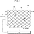
- FIGS. 3 and 4 illustrate that a touch screen included in a display device shown in FIG. 2 is implemented by an in-cell mutual capacitance sensor and an in-cell self-capacitance sensor.
- the display device 10 may be implemented based on a flat panel display, such as a liquid crystal display (LCD), a field emission display (FED), a plasma display panel (PDP), an organic light emitting diode (OLED) display, and an electrophoresis display (EPD).
- a flat panel display such as a liquid crystal display (LCD), a field emission display (FED), a plasma display panel (PDP), an organic light emitting diode (OLED) display, and an electrophoresis display (EPD).
- LCD liquid crystal display
- FED field emission display
- PDP plasma display panel
- OLED organic light emitting diode
- EPD electrophoresis display
- the display device 10 includes a display module and a touch module.
- the touch module includes a touch screen TSP and a touch driving device 18.
- the touch screen TSP may be implemented in a capacitive manner of sensing a touch input through a plurality of capacitive sensors.
- the touch screen TSP includes a plurality of touch sensors each having a capacitance.
- the capacitance may be divided into a self-capacitance and a mutual capacitance.
- the self-capacitance may be formed along a conductor line of a single layer formed in one direction, and the mutual capacitance may be formed between two conductor lines perpendicular to each other.
- a touch screen TSP implemented by mutual capacitance sensors Cm may include Tx electrode lines, Rx electrode lines crossing the Tx electrode lines, and touch sensors Cm respectively formed at crossings of the Tx electrode lines and the Rx electrode lines.
- the Tx electrode lines are driving signal lines supplying charges to the touch sensors Cm by applying a touch driving signal to each touch sensor Cm.
- the Rx electrode lines are sensor lines that are connected to the touch sensors Cm and supply charges of the touch sensors Cm to the touch driving device 18.
- a mutual capacitance sensing method charges are supplied to the touch sensors Cm by applying the touch driving signal to Tx electrodes through the Tx electrode lines, and changes in capacitances of the touch sensors Cm are sensed through Rx electrodes and the Rx electrode lines in synchronization with the touch driving signal, whereby a touch input may be recognized.
- electrodes 31 may be connected to sensor lines 32 formed along one direction, respectively.
- the self-capacitance sensors Cs each have a capacitance formed in each electrode 31.
- a self-capacitance sensing method when a touch driving signal is applied to the electrode 31 through the sensor line 32, charges Q are accumulated on the touch sensor Cs.
- a parasitic capacitance Cf is additionally connected to the self-capacitance sensor Cs, causing a total capacitance value to be changed. Because a capacitance of a sensor touched by the finger or the conductive object is different from a capacitance of a sensor which is not touched by the finger or the conductive object, whether or not a touch input is performed may be determined.
- the touch sensors Cm or Cs of the touch screen TSP may be embedded in a pixel array of a display panel DIS.
- a common electrode of pixels may be divided into a plurality of segments, so as to embed the touch sensors Cm or Cs in the pixel array.
- the touch sensors Cm or Cs may be implemented by divided common electrodes.
- Each common electrode segment may be commonly connected to the plurality of pixels and may form a touch sensor.
- a common voltage is applied to the common electrode of the pixels.
- a touch driving signal and a pen driving signal are applied to the common electrode of the pixels.
- the touch driving device 18 senses changes in charges of the touch sensor, determines whether or not a conductive material such as a finger (or a stylus pen) touches the touch screen TSP, detects a touch location when a touch input is performed, and calculates a coordinate value XY of the touch input. Further, the touch driving device 18 senses changes in charges of the touch sensor and generates information PAF about an additional function of the active stylus pen 20.
- the additional information PAF of the active stylus pen 20 includes pen pressure information, information about whether to use a button function (for example, an eraser function, a barrel function, etc.), and ID information.
- the display module may include the display panel DIS, a display driving circuit (12, 14, and 16), and a host system 19.
- the display panel DIS includes a liquid crystal layer between an upper substrate and a lower substrate.
- the pixel array of the display panel DIS includes pixels formed in pixel areas defined by data lines D1 to Dm and gate lines G1 to Gn, where m and n are a positive integer.
- Each pixel may include thin film transistors (TFTs) formed at crossings of the data lines D1 to Dm and the gate lines G1 to Gn, a pixel electrode charged with the data voltage, a storage capacitor that is connected to the pixel electrode and holds a voltage of a liquid crystal cell, and the like.
- TFTs thin film transistors
- Black matrixes, color filters, etc. may be formed on the upper substrate of the display panel DIS.
- the lower substrate of the display panel DIS may be configured in a COT (color filter on TFT) structure.
- the black matrixes and the color filters may be formed on the lower substrate of the display panel DIS.
- a common electrode supplied with the common voltage may be formed on the upper substrate or the lower substrate of the display panel DIS.
- Polarizing plates are respectively attached to the upper substrate and the lower substrate of the display panel DIS.
- Alignment layers for setting a pre-tilt angle of liquid crystals are respectively formed on the inner surfaces contacting the liquid crystals in the upper substrate and the lower substrate of the display panel DIS.
- a column spacer is formed between the upper substrate and the lower substrate of the display panel DIS to keep a cell gap of the liquid crystal cells constant.
- a backlight unit may be disposed under a back surface of the display panel DIS.
- the backlight unit may be implemented as one of an edge type backlight unit and a direct type backlight unit and may irradiate light onto the display panel DIS.
- the display panel DIS may be implemented in any known mode including a twisted nematic (TN) mode, a vertical alignment (VA) mode, an in-plane switching (IPS) mode, a fringe field switching (FFS) mode, etc.
- the display driving circuit includes a data driving circuit 12, a gate driving circuit 14, and a timing controller 16.
- the display driving circuit writes video data of an input image to the pixels of the display panel DIS.
- the data driving circuit 12 converts digital video data RGB received from the timing controller 16 into positive and negative analog gamma compensation voltages and outputs a data voltage.
- the data driving circuit 12 then supplies the data voltage to the data lines D1 to Dm.
- the gate driving circuit 14 sequentially supplies a gate pulse (or a scan pulse) synchronized with the data voltage to the gate lines G1 to Gn and selects pixel lines of the display panel DIS supplied with the data voltage.
- the timing controller 16 synchronizes operation timing of the data driving circuit 12 with operation timing of the gate driving circuit 14 based on timing signals, such as a vertical sync signal Vsync, a horizontal sync signal Hsync, a data enable signal DE, and a main clock MCLK, received from the host system 19.
- the timing controller 16 generates a data timing control signal and a scan timing control signal for respectively controlling the operation timings of the data driving circuit 12 and the gate driving circuit 14 using the timing signals.
- the data timing control signal includes a source sampling clock SSC, a source output enable signal SOE, a polarity control signal POL, etc.
- the scan timing control signal includes a gate start pulse GSP, a gate shift clock GSC, a gate output enable signal GOE, etc.
- the host system 19 may transmit the digital video data RGB and the timing signals Vsync, Hsync, DE, and MCLK to the timing controller 16 and execute an application program associated with touch coordinates information XY and the pen additional function input from the touch driving device 18.
- one frame is time-divided into at least one touch driving period TP (see FIG. 6 ) and a display driving period DP (see FIG. 6 ).
- the touch driving period TP is a period in which a touch sync signal Tsync (see FIG. 6 ) is maintained at a first voltage level
- the display driving period DP is a period in which the touch sync signal Tsync (see FIG. 6 ) is maintained at a second voltage level.
- the touch sync signal Tsync may be generated in the timing controller 16 or the host system 19.
- the data driving circuit 12 supplies the data voltage to the data lines D1 to Dm under the control of the timing controller 16, and the gate driving circuit 14 sequentially supplies the gate pulse synchronized with the data voltage to the gate lines G1 to Gn under the control of the timing controller 16.
- the touch driving device 18 stops operating.
- the touch driving device 18 applies a touch driving signal to the touch sensors of the touch screen TSP.
- the display driving circuit (12, 14, and 16) may supply an AC signal having the same amplitude and the same phase as the touch driving signal to the signal lines D1 to Dm and G1 to Gm, so as to minimize a parasitic capacitance between the signal lines D1 to Dm and G1 to Gn connected to the pixels and the touch sensors. In this instance, a display noise mixed in the touch sensing signal significantly decreases, and the accuracy of touch sensing increases.
- FIG. 5 illustrates an inner configuration of the active stylus pen according to the embodiment of the invention.
- FIG. 6 illustrates that a first pen driving signal and a second pen driving signal are successively outputs to the active stylus pen according to the embodiment of the invention in synchronization with a touch driving signal during a touch driving period.
- FIG. 7 illustrates a second pen driving signal that is generated in the active stylus pen according to the embodiment of the invention in synchronization with a touch driving signal using an amplitude modulation method.
- FIG. 8 illustrates a second pen driving signal that is generated in the active stylus pen according to the embodiment of the invention in synchronization with a touch driving signal using a frequency modulation method.
- the active stylus pen 20 includes a conductive tip 201, a switching unit 202 connected to the conductive tip 201, a receiving unit 203, an effectiveness checking unit 204, a pen driving signal generator 205, a parameter selector 206, and a transmitting unit 207.
- the active stylus pen 20 successively outputs a first pen driving signal PD1 and a second pen driving signal PD2 in synchronization with a touch driving signal TS.
- the conductive tip 201 is made of a conductive material, for example, metal and serves as a receiving electrode and a transmitting electrode.
- the conductive tip 201 is coupled with the touch screen TSP at a contact location.
- the conductive tip 201 receives a touch driving signal TS from the touch screen TSP at the contact location, the conductive tip 201 transmits a pen driving signal PS, that is generated inside the active stylus pen 20 so that it is synchronized with the touch driving signal TS, to the contact location of the touch screen TSP. Because the conductive tip 201 serves as the receiving electrode and the transmitting electrode, the active stylus pen 20 has an advantage of a simple structure.
- the switching unit 202 temporally separates reception timing of the touch driving signal TS from transmission timing of the pen driving signal PS.
- the switching unit 202 transmits the touch driving signal TS input from the touch screen TSP to the receiving unit 203 through the conductive tip 201 in an Rx mode and transmits the pen driving signal PS generated in the pen driving signal generator 205 to the touch screen TSP through the conductive tip 201 in a Tx mode.
- the receiving unit 203 includes at least one amplifier and a comparator and digitally processes the touch driving signal TS input through the switching unit 202.
- the effectiveness checking unit 204 analyzes the touch driving signal TS based on effective conditions of a predetermined default parameter set and checks the effectiveness of the touch driving signal TS. More specifically, as shown in FIG. 6 , when N successive pulses of a touch driving signal TS satisfy the effective conditions (for example, an effective period PE and an effective duty DT) of the predetermined default parameter set, the effectiveness checking unit 204 may determine the touch driving signal TS to be effective, where N is a positive integer equal to or greater than 2. In this instance, the effectiveness checking unit 204 changes the switching unit 202 from the Rx mode to the Tx mode.
- the effective conditions for example, an effective period PE and an effective duty DT
- the pen driving signal generator 205 When the effectiveness checking unit 204 determines the touch driving signal TS to be effective, the pen driving signal generator 205 generates a pen driving signal PS synchronized with the touch driving signal TS with reference to signal generation conditions of the default parameter set. In other words, the pen driving signal generator 205 may generate the pen driving signal PS synchronized with the touch driving signal TS based on the signal generation conditions (for example, a period, a duty, the number, etc.) of the default parameter set that is loaded to a register after a predetermined time passed from a conversion time point of the Tx mode.
- the signal generation conditions for example, a period, a duty, the number, etc.
- the pen driving signal PS includes a first pen driving signal PD1 for detecting a touch input and a second pen driving signal PD2 for detecting an additional input related to an additional function of the active stylus pen 20.
- the first pen driving signal PD1 is synchronized with a component of a first frequency f1 of the touch driving signal TS
- the second pen driving signal PD2 is synchronized with a component of a second frequency f2 of the touch driving signal TS.
- the touch driving signal TS may be input at the first frequency f1 during a first period of a touch driving period TP and may be input at the second frequency f2 during a second period of the touch driving period TP.
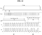
- the first frequency f1 and the second frequency f2 may be different from each other as shown in FIG. 11 , and may be substantially the same as each other as shown in FIG. 12 .
- the second pen driving signal PD2 when the first frequency f1 and the second frequency f2 are the same as each other, the second pen driving signal PD2 has the same frequency as the first pen driving signal PD1.
- the second pen driving signal PD2 when the first frequency f1 and the second frequency f2 are different from each other, the second pen driving signal PD2 has a frequency different from the first pen driving signal PD1.
- the second pen driving signal PD2 may have a frequency higher than the first pen driving signal PD1 by causing the second frequency f2 to be higher than the first frequency f1.
- the pen driving signal generator 205 may generate the second pen driving signal PD2 in synchronization with the component of the second frequency f2 of the touch driving signal TS through an amplitude modulation method shown in FIG. 7 .
- the pen driving signal generator 205 implements various additional functions, that are previously determined, by the second pen driving signal PD2 using a first voltage level V1 indicating digital information "1" and a second voltage level V2 that indicates digital information "0" and is less than the first voltage level V1.
- the second pen driving signal PD2 may be configured by various combinations of the first voltage level V1 and the second voltage level V2, for example, various combinations of first pulses each having a first amplitude A1 and second pulses each having a second amplitude A2.
- the pen driving signal generator 205 may generate the second pen driving signal PD2 in synchronization with the component of the second frequency f2 of the touch driving signal TS through a frequency modulation method shown in FIG. 8 .
- the pen driving signal generator 205 implements various additional functions, that are previously determined, by the second pen driving signal PD2 using a first frequency fa indicating digital information "1" and a second frequency fb that indicates digital information "0" and is faster than the first frequency fa.
- the second pen driving signal PD2 may be configured by various combinations of the first frequency fa and the second frequency fb, for example, various combinations of first pulses each having a first pulse width W1 and second pulses each having a second pulse width W2. Because a width and a frequency in the second pen driving signal PD2 are inversely proportional to each other, a pulse width W1 related to the first frequency fa is greater than a pulse width W2 related to the second frequency fb.
- the second pen driving signal PD2 has the same frequency as the first pen driving signal PD 1, and also includes a plurality of first pulses each having a first amplitude A1 and a plurality of second pulses each having a second amplitude A2 different from the first amplitude A1 as shown in FIG. 7 .
- the second pen driving signal PD2 has the same frequency as the first pen driving signal PD1, and also includes a plurality of first pulses each having a first pulse width W1 and a plurality of second pulses each having a second pulse width W2 different from the first pulse width W1 as shown in FIG. 8 .
- the second pen driving signal PD2 has a frequency higher than the first pen driving signal PD1, and also includes a plurality of first pulses each having a first amplitude A1 and a plurality of second pulses each having a second amplitude A2 different from the first amplitude A1 as shown in FIG. 7 .
- the second pen driving signal PD2 has a frequency higher than the first pen driving signal PD1, and also includes a plurality of first pulses each having a first pulse width W1 and a plurality of second pulses each having a second pulse width W2 different from the first pulse width W1 as shown in FIG. 8 .
- the transmitting unit 207 includes a level shifter. Thus, the transmitting unit 207 amplifies a voltage level of the pen driving signal PS input from the pen driving signal generator 205 and then applies the amplified pen driving signal PS to the switching unit 202.
- FIG. 9 illustrates the touch driving device included in the display device shown in FIG. 2 .
- FIG. 10 illustrates a configuration of the touch driving device for digitally processing a sensing value of a second pen driving signal.
- FIGS. 11 and 12 are waveform diagrams illustrating operation timing of the touch driving device shown in FIG. 9 .
- the touch driving device 18 may be implemented by an integrated circuit (IC) package.
- IC integrated circuit
- the touch driving device 18 includes a touch integrated IC SRIC and a microcontroller unit MCU.
- the touch integrated IC SRIC includes a sensing unit SUT, an analog-to-digital converter ADC, a comparator COMP, a digital controller CTR, a switching unit SW, etc.
- the sensing unit SUT is connected to the sensor lines of the touch screen TSP and applies the touch driving signal TS to the touch screen TSP. Further, the sensing unit SUT senses a touch input resulting from the first pen driving signal PD1 and senses an additional pen input resulting from the second pen driving signal PD2. To this end, the sensing unit SUT includes a touch driving signal supply unit (not shown), a touch sensor channel unit (or a channel multiplexer), a plurality of sensing units AFE, and a multiplexer unit MUX.
- the touch sensor channel unit is connected to electrodes of the touch sensors through the sensor lines (or the Rx electrode lines). The touch sensor channel unit connects the sensor lines to the sensing units AFE.
- the sensing units AFE sense an amount of charges of the touch sensors input through the sensor lines.
- the sensing units AFE sense an amount of charges resulting from the first pen driving signal PD1 input through the touch screen TSP during a first period SS1 of a touch driving period TP and sense an amount of charges resulting from the second pen driving signal PD2 input through the touch screen TSP during a second period SS2 of the touch driving period TP following the first period SS1.
- the multiplexer unit MUX selectively connects each of the sensing units AFE to the switching unit SW in first to nth touch driving periods (see FIGS. 11 and 12 ) in response to a touch sync signal Tsync.
- the switching unit SW is turned on and off in response to a time division control signal CONT from the digital controller CTR.
- the switching unit SW connects an output terminal of the sensing unit SUT to an input terminal of the analog-to-digital converter ADC during a first period SS1 of each of the first to nth touch driving periods. Further, the switching unit SW connects the output terminal of the sensing unit SUT to an input terminal of the comparator COMP during a second period SS2 of each of the first to nth touch driving periods.
- the analog-to-digital converter ADC converts an analog sensing value (namely, an amount of charges resulting from the first pen driving signal PD1) corresponding to a touch input into a digital touch sensing value.
- the comparator COMP compares an analog sensing value (namely, an amount of charges resulting from the second pen driving signal PD2) corresponding to an additional input with a predetermined reference value Vref and generates a digital additional sensing value.
- an analog sensing value namely, an amount of charges resulting from the second pen driving signal PD2
- Vref a predetermined reference value
- the second pen driving signal PD2 is configured by a combination of the first voltage level V1 and the second voltage level V2 in accordance with the amplitude modulation method shown in FIG.
- an amount of charges resulting from the first voltage level V1 may be greater than the reference value Vref and thus may be generated as digital information "1”
- an amount of charges resulting from the second voltage level V2 may be less than the reference value Vref and thus may be generated as digital information "0”.
- the second pen driving signal PD2 is configured by a combination of the first frequency fa and the second frequency fb in accordance with the frequency modulation method shown in FIG. 8
- an amount of charges resulting from the first frequency fa may be greater than the reference value Vref and thus may be generated as digital information "1”
- an amount of charges resulting from the second frequency fb may be less than the reference value Vref and thus may be generated as digital information "0".
- the digital controller CTR stores the digital touch sensing value from the analog-to-digital converter ADC in a first memory and stores the digital additional sensing value from the comparator COMP in a second memory.
- the digital controller CTR generates the time division control signal CONT for dividing each of the first to nth touch driving periods into a first period SS1 and a second period SS2 and supplies the time division control signal CONT to the switching unit SW.
- the digital controller CTR transmits the digital touch sensing value stored in the first memory and the digital additional sensing value stored in the second memory to the microcontroller unit MCU through a serial peripheral interface (SPI).
- SPI serial peripheral interface
- the microcontroller unit MCU calculates a coordinate value of a touch input based on the digital touch sensing value and generates information about the additional function of the active stylus pen based on the digital additional sensing value.
- the microcontroller unit MCU then transmits touch coordinate information XY and information PAF about the pen additional function to the host system.
- FIGS. 13 and 14 illustrate a second pen driving signal generated in three states in synchronization with a touch driving signal in the active stylus pen according to the embodiment of the invention.
- FIG. 15 illustrates an amount of information that can be transmitted when a second pen driving signal is generated in three states.
- the active stylus pen generates first pen driving signals Pen1, ..., Pen4, ..., in some of touch driving periods TP of one frame and generates second pen driving signals Data1, ..., Data6, ..., in remaining touch driving periods TP of one frame.
- the first pen driving signals Pen1, ..., Pen4, ..., and the second pen driving signals Data1, ..., Data6, ..., are output to the touch screen with a display driving period DP interposed between them.
- a first period of the touch driving period, in which the first pen driving signals Pen1, ..., Pen4, ..., are generated, and a second period of the touch driving period, in which the second pen driving signals Data1, ..., Data6, ..., are generated, are disposed in different touch driving periods TP with the display driving period DP interposed between them.
- the sensing sensitivity of the additional input can be improved. Furthermore, because the first pen driving signals Pen1, ..., Pen4, ..., and the second pen driving signals Data1, ..., Data6, ..., are output to the touch screen with the display driving period DP interposed between them, sensing data may be processed during the display driving period DP. Hence, time required in the data processing can be sufficiently secured.
- the second pen driving signals Data1, ..., Data6, ... may have three states so as to increase a transmission amount of information about the additional input.
- the second pen driving signals Data1, ..., Data6, ..., of the three states may include first state (indicated by '0') signals having the same phase as a touch driving signal TS, second state (indicated by '1') signals having a phase opposite the touch driving signal TS, and third state (indicated by 'passive') signals for not driving the active stylus pen.
- the second pen driving signals Data1, ..., Data6, ... are implemented in the three states, much more information about the additional function can be transmitted using limited data amount because the embodiment of the invention can create an effect of 3-bit data using 2-bit data. Hence, it is easy to achieve a high performance of the active stylus pen. Further, because the second pen driving signals of the three states can achieve the same performance for a shorter driving time compared to when the second pen driving signals are implemented in two states ('0' and '1'), the second pen driving signals of the three states are effective in a reduction in power consumption.
- the touch driving signal TS may have the same frequency in the first period of the touch driving period in which the first pen driving signals Pen1, ..., Pen4, ..., are generated, and the second period of the touch driving period in which the second pen driving signals Data1, ..., Data6, ..., are generated.
- the second pen driving signals Data1, ..., Data6, ... may have the same frequency as the first pen driving signals Pen1, ..., Pen4, ..., and may also include first state (indicated by '0') signals having the same phase as the touch driving signal TS, second state (indicated by '1') signals having a phase opposite the touch driving signal TS, and third state (indicated by 'passive') signals for not driving the active stylus pen.
- the touch driving signal TS may have a higher frequency in the second period of the touch driving period, in which the second pen driving signals Data1, ..., Data6, ..., are generated, than in the first period of the touch driving period in which the first pen driving signals Pen1, ..., Pen4, ..., are generated.
- the second pen driving signals Data1, ..., Data6, ... may have a frequency higher than the first pen driving signals Pen1, ..., Pen4, ..., and may also include first state (indicated by '0') signals having the same phase as the touch driving signal TS, second state (indicated by '1') signals having a phase opposite the touch driving signal TS, and third state (indicated by 'passive') signals for not driving the active stylus pen.
- 'Beacon' indicates a signal instructing the active stylus pen of a pen frequency, a pen driving method (for example, contact, hovering, etc.), a driving status (for example, a basic drive, a low power drive, etc.) of the display panel, etc.
- the embodiment of the invention has the following effects.
Landscapes
- Engineering & Computer Science (AREA)
- General Engineering & Computer Science (AREA)
- Theoretical Computer Science (AREA)
- Human Computer Interaction (AREA)
- Physics & Mathematics (AREA)
- General Physics & Mathematics (AREA)
- Position Input By Displaying (AREA)
Applications Claiming Priority (2)
| Application Number | Priority Date | Filing Date | Title |
|---|---|---|---|
| KR20150191807 | 2015-12-31 | ||
| KR1020160163495A KR102607842B1 (ko) | 2015-12-31 | 2016-12-02 | 능동형 스타일러스 펜을 포함한 터치 센싱 시스템 |
Publications (3)
| Publication Number | Publication Date |
|---|---|
| EP3190490A2 true EP3190490A2 (de) | 2017-07-12 |
| EP3190490A3 EP3190490A3 (de) | 2017-09-06 |
| EP3190490B1 EP3190490B1 (de) | 2022-09-28 |
Family
ID=57680090
Family Applications (1)
| Application Number | Title | Priority Date | Filing Date |
|---|---|---|---|
| EP16205763.2A Active EP3190490B1 (de) | 2015-12-31 | 2016-12-21 | Berührungsempfindliches system mit aktivem eingabestift |
Country Status (2)
| Country | Link |
|---|---|
| US (1) | US10474280B2 (de) |
| EP (1) | EP3190490B1 (de) |
Families Citing this family (28)
| Publication number | Priority date | Publication date | Assignee | Title |
|---|---|---|---|---|
| US10579169B2 (en) | 2016-03-08 | 2020-03-03 | Egalax_Empia Technology Inc. | Stylus and touch control apparatus for detecting tilt angle of stylus and control method thereof |
| CN112416149B (zh) | 2016-03-08 | 2024-08-20 | 禾瑞亚科技股份有限公司 | 侦测触控笔的倾斜角的触控控制装置与其控制方法 |
| EP3525069B1 (de) * | 2016-10-06 | 2021-03-17 | Wacom Co., Ltd. | Eingabestift und steuergerät |
| KR102780729B1 (ko) * | 2016-12-13 | 2025-03-12 | 엘지디스플레이 주식회사 | 터치 센서를 갖는 전자장치와 이의 구동 방법 |
| CN117348746A (zh) | 2017-02-22 | 2024-01-05 | 株式会社和冠 | 主动式触控笔、控制器集成电路及其执行的方法 |
| US10627957B2 (en) * | 2017-02-22 | 2020-04-21 | Synaptics Incorporated | Active avoidance of display noise in simultaneous touch and display |
| US10216333B2 (en) * | 2017-06-30 | 2019-02-26 | Microsoft Technology Licensing, Llc | Phase error compensation in single correlator systems |
| US10528158B2 (en) * | 2017-08-07 | 2020-01-07 | Himax Technologies Limited | Active stylus, touch sensor, and signal transmission and sensing method for active stylus and touch sensor |
| KR102371154B1 (ko) * | 2017-09-29 | 2022-03-07 | 엘지디스플레이 주식회사 | 터치 표시 장치, 터치 회로, 펜, 터치 시스템 및 멀티 펜 센싱 방법 |
| CN108235746B (zh) * | 2017-12-27 | 2020-10-20 | 深圳市汇顶科技股份有限公司 | 信号发射方法及主动笔、信号接收方法及触摸屏 |
| KR102410015B1 (ko) * | 2017-12-27 | 2022-06-16 | 삼성전자주식회사 | 터치 스크린 컨트롤러, 이를 포함하는 터치 스크린 시스템 및 터치 스크린 컨트롤러의 동작방법 |
| KR102436435B1 (ko) * | 2018-03-13 | 2022-08-26 | 삼성전자주식회사 | 전자 펜으로부터 수신한 신호에 기초하여 다양한 기능을 실행시키기 위한 전자 장치 |
| KR102347140B1 (ko) * | 2018-10-25 | 2022-01-03 | 솔로몬 시스테크 (선전) 리미티드 | 수동형 유기 발광 다이오드 디스플레이 |
| KR102601347B1 (ko) * | 2018-12-28 | 2023-11-13 | 엘지디스플레이 주식회사 | 터치표시장치 및 터치센싱회로 |
| KR102206051B1 (ko) * | 2019-01-22 | 2021-01-21 | 주식회사 하이딥 | 터치 장치 및 이의 터치 검출 방법 |
| KR102764364B1 (ko) * | 2019-06-12 | 2025-02-07 | 주식회사 하이딥 | 터치 장치 및 이의 터치 검출 방법 |
| KR102792337B1 (ko) * | 2019-11-04 | 2025-04-09 | 삼성디스플레이 주식회사 | 표시장치 |
| JP7481789B2 (ja) * | 2020-07-01 | 2024-05-13 | パナソニックオートモーティブシステムズ株式会社 | 表示装置、制御装置および制御方法 |
| CN114846435B (zh) * | 2020-09-14 | 2024-12-17 | 深圳市汇顶科技股份有限公司 | 无线通信的方法、主动笔、触摸屏、电子设备和通信系统 |
| TWI768734B (zh) | 2021-02-26 | 2022-06-21 | 奕力科技股份有限公司 | 觸控裝置以及其觸控筆 |
| JP2022191080A (ja) * | 2021-06-15 | 2022-12-27 | 株式会社ジャパンディスプレイ | 入力検出システム及び検出装置 |
| TWM620145U (zh) | 2021-08-05 | 2021-11-21 | 奕力科技股份有限公司 | 觸控面板以及觸控輸入系統 |
| US11656726B1 (en) * | 2022-02-09 | 2023-05-23 | Novatek Microelectronics Corp. | Control circuit, electronic device, and control method for stylus pen interacting with touch panel |
| US11747939B1 (en) * | 2022-05-09 | 2023-09-05 | Pixart Imaging Inc. | Capacitive touch control system with frequency booster |
| KR20240000691A (ko) * | 2022-06-23 | 2024-01-03 | 삼성디스플레이 주식회사 | 표시 장치 및 이를 포함하는 터치 센싱 시스템 |
| KR20240039635A (ko) | 2022-09-19 | 2024-03-27 | 삼성디스플레이 주식회사 | 전자 장치 |
| TWI824935B (zh) * | 2023-02-09 | 2023-12-01 | 大陸商北京集創北方科技股份有限公司 | 主動式觸控筆之觸控檢測方法、觸控裝置及資訊處理裝置 |
| TW202522736A (zh) * | 2023-11-22 | 2025-06-01 | 群創光電股份有限公司 | 電子裝置 |
Family Cites Families (13)
| Publication number | Priority date | Publication date | Assignee | Title |
|---|---|---|---|---|
| KR20040061488A (ko) | 2002-12-31 | 2004-07-07 | 엘지.필립스 엘시디 주식회사 | 능동행렬 유기전기발광소자 |
| US7288946B2 (en) * | 2005-06-03 | 2007-10-30 | Synaptics Incorporated | Methods and systems for detecting a capacitance using sigma-delta measurement techniques |
| KR101310378B1 (ko) | 2008-11-19 | 2013-09-23 | 엘지디스플레이 주식회사 | 액정표시장치 |
| KR101073309B1 (ko) | 2009-11-24 | 2011-10-12 | 삼성모바일디스플레이주식회사 | 터치 스크린 시스템 및 그 구동방법 |
| JP5345050B2 (ja) | 2009-12-25 | 2013-11-20 | 株式会社ワコム | 指示体、位置検出装置及び位置検出方法 |
| US9176630B2 (en) * | 2010-08-30 | 2015-11-03 | Perceptive Pixel, Inc. | Localizing an electrostatic stylus within a capacitive touch sensor |
| US9310911B2 (en) * | 2011-07-29 | 2016-04-12 | Sharp Kabushiki Kaisha | Display device |
| CN102866792B (zh) | 2012-08-20 | 2016-06-01 | 深圳市汇顶科技股份有限公司 | 一种触摸笔、触摸控制器、触摸检测系统及其方法 |
| US9158393B2 (en) | 2012-12-18 | 2015-10-13 | Logitech Europe S.A. | Active stylus for touch sensing applications |
| US9946366B2 (en) | 2013-06-03 | 2018-04-17 | Apple Inc. | Display, touch, and stylus synchronization |
| US9939935B2 (en) * | 2013-07-31 | 2018-04-10 | Apple Inc. | Scan engine for touch controller architecture |
| KR102181293B1 (ko) | 2013-12-31 | 2020-11-20 | 엘지디스플레이 주식회사 | 터치 센서 내장형 표시 장치와 그 구동 장치 및 그 구동 방법 |
| CN106462306B (zh) | 2014-06-27 | 2020-09-29 | 3M创新有限公司 | 触摸系统触笔和方法 |
-
2016
- 2016-12-16 US US15/381,410 patent/US10474280B2/en active Active
- 2016-12-21 EP EP16205763.2A patent/EP3190490B1/de active Active
Non-Patent Citations (1)
| Title |
|---|
| None |
Also Published As
| Publication number | Publication date |
|---|---|
| EP3190490B1 (de) | 2022-09-28 |
| EP3190490A3 (de) | 2017-09-06 |
| US10474280B2 (en) | 2019-11-12 |
| US20170192591A1 (en) | 2017-07-06 |
Similar Documents
| Publication | Publication Date | Title |
|---|---|---|
| EP3190490B1 (de) | Berührungsempfindliches system mit aktivem eingabestift | |
| KR102607842B1 (ko) | 능동형 스타일러스 펜을 포함한 터치 센싱 시스템 | |
| US10496205B2 (en) | Touch sensing system and method of driving the same | |
| CN107272921B (zh) | 有源触控笔、包括其的触摸感测系统和触摸感测方法 | |
| US10691228B2 (en) | Electronic device having touch sensor and method of driving the same | |
| CN106484178B (zh) | 触控笔、触摸感测系统以及触摸感测系统的驱动方法 | |
| US10324547B2 (en) | Active stylus pen, touch sensing system and driving method thereof | |
| KR102340937B1 (ko) | 스타일러스 펜, 및 터치 센싱 시스템과 그 구동방법 | |
| US9891747B2 (en) | Multi-touch sensitive display device and method for assigning touch identification therein | |
| KR102050385B1 (ko) | 터치 센싱 시스템과 그 지연 시간 감소 방법 | |
| KR102520695B1 (ko) | 능동형 스타일러스 펜과 그를 포함한 터치 센싱 시스템, 및 그 구동방법 | |
| US9335861B2 (en) | Touch sensing system and driving method thereof, and display device using the touch sensing system | |
| KR102364099B1 (ko) | 능동형 스타일러스 펜과 그를 포함한 터치 센싱 시스템, 및 그 구동방법 | |
| US11467679B2 (en) | Touch screen device | |
| KR101667078B1 (ko) | 터치 센싱 장치와 시스템 및 그 터치 레포트 레이트 향상 방법 | |
| KR20170052815A (ko) | 능동형 스타일러스 펜과 그 구동방법 및, 능동형 스타일러스 펜을 포함한 터치 센싱 시스템 |
Legal Events
| Date | Code | Title | Description |
|---|---|---|---|
| PUAI | Public reference made under article 153(3) epc to a published international application that has entered the european phase |
Free format text: ORIGINAL CODE: 0009012 |
|
| STAA | Information on the status of an ep patent application or granted ep patent |
Free format text: STATUS: REQUEST FOR EXAMINATION WAS MADE |
|
| 17P | Request for examination filed |
Effective date: 20161221 |
|
| AK | Designated contracting states |
Kind code of ref document: A2 Designated state(s): AL AT BE BG CH CY CZ DE DK EE ES FI FR GB GR HR HU IE IS IT LI LT LU LV MC MK MT NL NO PL PT RO RS SE SI SK SM TR |
|
| AX | Request for extension of the european patent |
Extension state: BA ME |
|
| PUAL | Search report despatched |
Free format text: ORIGINAL CODE: 0009013 |
|
| AK | Designated contracting states |
Kind code of ref document: A3 Designated state(s): AL AT BE BG CH CY CZ DE DK EE ES FI FR GB GR HR HU IE IS IT LI LT LU LV MC MK MT NL NO PL PT RO RS SE SI SK SM TR |
|
| AX | Request for extension of the european patent |
Extension state: BA ME |
|
| RIC1 | Information provided on ipc code assigned before grant |
Ipc: G06F 3/038 20130101ALI20170803BHEP Ipc: G06F 3/041 20060101AFI20170803BHEP Ipc: G06F 3/044 20060101ALI20170803BHEP Ipc: G06F 3/0354 20130101ALI20170803BHEP |
|
| RBV | Designated contracting states (corrected) |
Designated state(s): AL AT BE BG CH CY CZ DE DK EE ES FI FR GB GR HR HU IE IS IT LI LT LU LV MC MK MT NL NO PL PT RO RS SE SI SK SM TR |
|
| STAA | Information on the status of an ep patent application or granted ep patent |
Free format text: STATUS: EXAMINATION IS IN PROGRESS |
|
| 17Q | First examination report despatched |
Effective date: 20190524 |
|
| GRAP | Despatch of communication of intention to grant a patent |
Free format text: ORIGINAL CODE: EPIDOSNIGR1 |
|
| STAA | Information on the status of an ep patent application or granted ep patent |
Free format text: STATUS: GRANT OF PATENT IS INTENDED |
|
| INTG | Intention to grant announced |
Effective date: 20220422 |
|
| GRAS | Grant fee paid |
Free format text: ORIGINAL CODE: EPIDOSNIGR3 |
|
| GRAA | (expected) grant |
Free format text: ORIGINAL CODE: 0009210 |
|
| STAA | Information on the status of an ep patent application or granted ep patent |
Free format text: STATUS: THE PATENT HAS BEEN GRANTED |
|
| AK | Designated contracting states |
Kind code of ref document: B1 Designated state(s): AL AT BE BG CH CY CZ DE DK EE ES FI FR GB GR HR HU IE IS IT LI LT LU LV MC MK MT NL NO PL PT RO RS SE SI SK SM TR |
|
| REG | Reference to a national code |
Ref country code: GB Ref legal event code: FG4D |
|
| REG | Reference to a national code |
Ref country code: CH Ref legal event code: EP |
|
| REG | Reference to a national code |
Ref country code: DE Ref legal event code: R096 Ref document number: 602016075253 Country of ref document: DE |
|
| REG | Reference to a national code |
Ref country code: AT Ref legal event code: REF Ref document number: 1521664 Country of ref document: AT Kind code of ref document: T Effective date: 20221015 |
|
| REG | Reference to a national code |
Ref country code: IE Ref legal event code: FG4D |
|
| REG | Reference to a national code |
Ref country code: LT Ref legal event code: MG9D |
|
| PG25 | Lapsed in a contracting state [announced via postgrant information from national office to epo] |
Ref country code: SE Free format text: LAPSE BECAUSE OF FAILURE TO SUBMIT A TRANSLATION OF THE DESCRIPTION OR TO PAY THE FEE WITHIN THE PRESCRIBED TIME-LIMIT Effective date: 20220928 Ref country code: RS Free format text: LAPSE BECAUSE OF FAILURE TO SUBMIT A TRANSLATION OF THE DESCRIPTION OR TO PAY THE FEE WITHIN THE PRESCRIBED TIME-LIMIT Effective date: 20220928 Ref country code: NO Free format text: LAPSE BECAUSE OF FAILURE TO SUBMIT A TRANSLATION OF THE DESCRIPTION OR TO PAY THE FEE WITHIN THE PRESCRIBED TIME-LIMIT Effective date: 20221228 Ref country code: LV Free format text: LAPSE BECAUSE OF FAILURE TO SUBMIT A TRANSLATION OF THE DESCRIPTION OR TO PAY THE FEE WITHIN THE PRESCRIBED TIME-LIMIT Effective date: 20220928 Ref country code: LT Free format text: LAPSE BECAUSE OF FAILURE TO SUBMIT A TRANSLATION OF THE DESCRIPTION OR TO PAY THE FEE WITHIN THE PRESCRIBED TIME-LIMIT Effective date: 20220928 Ref country code: FI Free format text: LAPSE BECAUSE OF FAILURE TO SUBMIT A TRANSLATION OF THE DESCRIPTION OR TO PAY THE FEE WITHIN THE PRESCRIBED TIME-LIMIT Effective date: 20220928 |
|
| REG | Reference to a national code |
Ref country code: NL Ref legal event code: MP Effective date: 20220928 |
|
| REG | Reference to a national code |
Ref country code: AT Ref legal event code: MK05 Ref document number: 1521664 Country of ref document: AT Kind code of ref document: T Effective date: 20220928 |
|
| PG25 | Lapsed in a contracting state [announced via postgrant information from national office to epo] |
Ref country code: HR Free format text: LAPSE BECAUSE OF FAILURE TO SUBMIT A TRANSLATION OF THE DESCRIPTION OR TO PAY THE FEE WITHIN THE PRESCRIBED TIME-LIMIT Effective date: 20220928 Ref country code: GR Free format text: LAPSE BECAUSE OF FAILURE TO SUBMIT A TRANSLATION OF THE DESCRIPTION OR TO PAY THE FEE WITHIN THE PRESCRIBED TIME-LIMIT Effective date: 20221229 |
|
| PG25 | Lapsed in a contracting state [announced via postgrant information from national office to epo] |
Ref country code: SM Free format text: LAPSE BECAUSE OF FAILURE TO SUBMIT A TRANSLATION OF THE DESCRIPTION OR TO PAY THE FEE WITHIN THE PRESCRIBED TIME-LIMIT Effective date: 20220928 Ref country code: RO Free format text: LAPSE BECAUSE OF FAILURE TO SUBMIT A TRANSLATION OF THE DESCRIPTION OR TO PAY THE FEE WITHIN THE PRESCRIBED TIME-LIMIT Effective date: 20220928 Ref country code: PT Free format text: LAPSE BECAUSE OF FAILURE TO SUBMIT A TRANSLATION OF THE DESCRIPTION OR TO PAY THE FEE WITHIN THE PRESCRIBED TIME-LIMIT Effective date: 20230130 Ref country code: ES Free format text: LAPSE BECAUSE OF FAILURE TO SUBMIT A TRANSLATION OF THE DESCRIPTION OR TO PAY THE FEE WITHIN THE PRESCRIBED TIME-LIMIT Effective date: 20220928 Ref country code: CZ Free format text: LAPSE BECAUSE OF FAILURE TO SUBMIT A TRANSLATION OF THE DESCRIPTION OR TO PAY THE FEE WITHIN THE PRESCRIBED TIME-LIMIT Effective date: 20220928 Ref country code: AT Free format text: LAPSE BECAUSE OF FAILURE TO SUBMIT A TRANSLATION OF THE DESCRIPTION OR TO PAY THE FEE WITHIN THE PRESCRIBED TIME-LIMIT Effective date: 20220928 |
|
| PG25 | Lapsed in a contracting state [announced via postgrant information from national office to epo] |
Ref country code: SK Free format text: LAPSE BECAUSE OF FAILURE TO SUBMIT A TRANSLATION OF THE DESCRIPTION OR TO PAY THE FEE WITHIN THE PRESCRIBED TIME-LIMIT Effective date: 20220928 Ref country code: PL Free format text: LAPSE BECAUSE OF FAILURE TO SUBMIT A TRANSLATION OF THE DESCRIPTION OR TO PAY THE FEE WITHIN THE PRESCRIBED TIME-LIMIT Effective date: 20220928 Ref country code: IS Free format text: LAPSE BECAUSE OF FAILURE TO SUBMIT A TRANSLATION OF THE DESCRIPTION OR TO PAY THE FEE WITHIN THE PRESCRIBED TIME-LIMIT Effective date: 20230128 Ref country code: EE Free format text: LAPSE BECAUSE OF FAILURE TO SUBMIT A TRANSLATION OF THE DESCRIPTION OR TO PAY THE FEE WITHIN THE PRESCRIBED TIME-LIMIT Effective date: 20220928 |
|
| REG | Reference to a national code |
Ref country code: DE Ref legal event code: R097 Ref document number: 602016075253 Country of ref document: DE |
|
| PG25 | Lapsed in a contracting state [announced via postgrant information from national office to epo] |
Ref country code: NL Free format text: LAPSE BECAUSE OF FAILURE TO SUBMIT A TRANSLATION OF THE DESCRIPTION OR TO PAY THE FEE WITHIN THE PRESCRIBED TIME-LIMIT Effective date: 20220928 Ref country code: AL Free format text: LAPSE BECAUSE OF FAILURE TO SUBMIT A TRANSLATION OF THE DESCRIPTION OR TO PAY THE FEE WITHIN THE PRESCRIBED TIME-LIMIT Effective date: 20220928 |
|
| PG25 | Lapsed in a contracting state [announced via postgrant information from national office to epo] |
Ref country code: DK Free format text: LAPSE BECAUSE OF FAILURE TO SUBMIT A TRANSLATION OF THE DESCRIPTION OR TO PAY THE FEE WITHIN THE PRESCRIBED TIME-LIMIT Effective date: 20220928 |
|
| REG | Reference to a national code |
Ref country code: CH Ref legal event code: PL |
|
| PLBE | No opposition filed within time limit |
Free format text: ORIGINAL CODE: 0009261 |
|
| STAA | Information on the status of an ep patent application or granted ep patent |
Free format text: STATUS: NO OPPOSITION FILED WITHIN TIME LIMIT |
|
| REG | Reference to a national code |
Ref country code: BE Ref legal event code: MM Effective date: 20221231 |
|
| PG25 | Lapsed in a contracting state [announced via postgrant information from national office to epo] |
Ref country code: LU Free format text: LAPSE BECAUSE OF NON-PAYMENT OF DUE FEES Effective date: 20221221 |
|
| 26N | No opposition filed |
Effective date: 20230629 |
|
| PG25 | Lapsed in a contracting state [announced via postgrant information from national office to epo] |
Ref country code: LI Free format text: LAPSE BECAUSE OF NON-PAYMENT OF DUE FEES Effective date: 20221231 Ref country code: IE Free format text: LAPSE BECAUSE OF NON-PAYMENT OF DUE FEES Effective date: 20221221 Ref country code: CH Free format text: LAPSE BECAUSE OF NON-PAYMENT OF DUE FEES Effective date: 20221231 |
|
| PG25 | Lapsed in a contracting state [announced via postgrant information from national office to epo] |
Ref country code: SI Free format text: LAPSE BECAUSE OF FAILURE TO SUBMIT A TRANSLATION OF THE DESCRIPTION OR TO PAY THE FEE WITHIN THE PRESCRIBED TIME-LIMIT Effective date: 20220928 Ref country code: BE Free format text: LAPSE BECAUSE OF NON-PAYMENT OF DUE FEES Effective date: 20221231 |
|
| PG25 | Lapsed in a contracting state [announced via postgrant information from national office to epo] |
Ref country code: HU Free format text: LAPSE BECAUSE OF FAILURE TO SUBMIT A TRANSLATION OF THE DESCRIPTION OR TO PAY THE FEE WITHIN THE PRESCRIBED TIME-LIMIT; INVALID AB INITIO Effective date: 20161221 |
|
| PG25 | Lapsed in a contracting state [announced via postgrant information from national office to epo] |
Ref country code: CY Free format text: LAPSE BECAUSE OF FAILURE TO SUBMIT A TRANSLATION OF THE DESCRIPTION OR TO PAY THE FEE WITHIN THE PRESCRIBED TIME-LIMIT Effective date: 20220928 |
|
| PG25 | Lapsed in a contracting state [announced via postgrant information from national office to epo] |
Ref country code: MK Free format text: LAPSE BECAUSE OF FAILURE TO SUBMIT A TRANSLATION OF THE DESCRIPTION OR TO PAY THE FEE WITHIN THE PRESCRIBED TIME-LIMIT Effective date: 20220928 Ref country code: IT Free format text: LAPSE BECAUSE OF FAILURE TO SUBMIT A TRANSLATION OF THE DESCRIPTION OR TO PAY THE FEE WITHIN THE PRESCRIBED TIME-LIMIT Effective date: 20220928 |
|
| PG25 | Lapsed in a contracting state [announced via postgrant information from national office to epo] |
Ref country code: MC Free format text: LAPSE BECAUSE OF FAILURE TO SUBMIT A TRANSLATION OF THE DESCRIPTION OR TO PAY THE FEE WITHIN THE PRESCRIBED TIME-LIMIT Effective date: 20220928 |
|
| PG25 | Lapsed in a contracting state [announced via postgrant information from national office to epo] |
Ref country code: TR Free format text: LAPSE BECAUSE OF FAILURE TO SUBMIT A TRANSLATION OF THE DESCRIPTION OR TO PAY THE FEE WITHIN THE PRESCRIBED TIME-LIMIT Effective date: 20220928 Ref country code: MC Free format text: LAPSE BECAUSE OF FAILURE TO SUBMIT A TRANSLATION OF THE DESCRIPTION OR TO PAY THE FEE WITHIN THE PRESCRIBED TIME-LIMIT Effective date: 20220928 |
|
| PG25 | Lapsed in a contracting state [announced via postgrant information from national office to epo] |
Ref country code: BG Free format text: LAPSE BECAUSE OF FAILURE TO SUBMIT A TRANSLATION OF THE DESCRIPTION OR TO PAY THE FEE WITHIN THE PRESCRIBED TIME-LIMIT Effective date: 20220928 |
|
| PG25 | Lapsed in a contracting state [announced via postgrant information from national office to epo] |
Ref country code: MT Free format text: LAPSE BECAUSE OF FAILURE TO SUBMIT A TRANSLATION OF THE DESCRIPTION OR TO PAY THE FEE WITHIN THE PRESCRIBED TIME-LIMIT Effective date: 20220928 |
|
| PGFP | Annual fee paid to national office [announced via postgrant information from national office to epo] |
Ref country code: DE Payment date: 20251020 Year of fee payment: 10 |
|
| PGFP | Annual fee paid to national office [announced via postgrant information from national office to epo] |
Ref country code: GB Payment date: 20251023 Year of fee payment: 10 |
|
| PGFP | Annual fee paid to national office [announced via postgrant information from national office to epo] |
Ref country code: FR Payment date: 20251021 Year of fee payment: 10 |