EP3190657B1 - Réseau d'antennes structural et son procédé de fabrication - Google Patents
Réseau d'antennes structural et son procédé de fabrication Download PDFInfo
- Publication number
- EP3190657B1 EP3190657B1 EP17150149.7A EP17150149A EP3190657B1 EP 3190657 B1 EP3190657 B1 EP 3190657B1 EP 17150149 A EP17150149 A EP 17150149A EP 3190657 B1 EP3190657 B1 EP 3190657B1
- Authority
- EP
- European Patent Office
- Prior art keywords
- substrate layer
- structural
- skin
- antenna
- wall sections
- Prior art date
- Legal status (The legal status is an assumption and is not a legal conclusion. Google has not performed a legal analysis and makes no representation as to the accuracy of the status listed.)
- Active
Links
Images


Classifications
-
- H—ELECTRICITY
- H01—ELECTRIC ELEMENTS
- H01Q—ANTENNAS, i.e. RADIO AERIALS
- H01Q21/00—Antenna arrays or systems
- H01Q21/06—Arrays of individually energised antenna units similarly polarised and spaced apart
- H01Q21/061—Two dimensional planar arrays
- H01Q21/062—Two dimensional planar arrays using dipole aerials
-
- H—ELECTRICITY
- H01—ELECTRIC ELEMENTS
- H01Q—ANTENNAS, i.e. RADIO AERIALS
- H01Q1/00—Details of, or arrangements associated with, antennas
- H01Q1/12—Supports; Mounting means
-
- H—ELECTRICITY
- H01—ELECTRIC ELEMENTS
- H01Q—ANTENNAS, i.e. RADIO AERIALS
- H01Q1/00—Details of, or arrangements associated with, antennas
- H01Q1/27—Adaptation for use in or on movable bodies
- H01Q1/28—Adaptation for use in or on aircraft, missiles, satellites, or balloons
-
- H—ELECTRICITY
- H01—ELECTRIC ELEMENTS
- H01Q—ANTENNAS, i.e. RADIO AERIALS
- H01Q1/00—Details of, or arrangements associated with, antennas
- H01Q1/27—Adaptation for use in or on movable bodies
- H01Q1/28—Adaptation for use in or on aircraft, missiles, satellites, or balloons
- H01Q1/286—Adaptation for use in or on aircraft, missiles, satellites, or balloons substantially flush mounted with the skin of the craft
-
- H—ELECTRICITY
- H01—ELECTRIC ELEMENTS
- H01Q—ANTENNAS, i.e. RADIO AERIALS
- H01Q1/00—Details of, or arrangements associated with, antennas
- H01Q1/36—Structural form of radiating elements, e.g. cone, spiral, umbrella; Particular materials used therewith
- H01Q1/38—Structural form of radiating elements, e.g. cone, spiral, umbrella; Particular materials used therewith formed by a conductive layer on an insulating support
-
- H—ELECTRICITY
- H01—ELECTRIC ELEMENTS
- H01Q—ANTENNAS, i.e. RADIO AERIALS
- H01Q1/00—Details of, or arrangements associated with, antennas
- H01Q1/50—Structural association of antennas with earthing switches, lead-in devices or lightning protectors
-
- H—ELECTRICITY
- H01—ELECTRIC ELEMENTS
- H01Q—ANTENNAS, i.e. RADIO AERIALS
- H01Q21/00—Antenna arrays or systems
-
- H—ELECTRICITY
- H01—ELECTRIC ELEMENTS
- H01Q—ANTENNAS, i.e. RADIO AERIALS
- H01Q21/00—Antenna arrays or systems
- H01Q21/0006—Particular feeding systems
-
- H—ELECTRICITY
- H01—ELECTRIC ELEMENTS
- H01Q—ANTENNAS, i.e. RADIO AERIALS
- H01Q21/00—Antenna arrays or systems
- H01Q21/0087—Apparatus or processes specially adapted for manufacturing antenna arrays
-
- H—ELECTRICITY
- H01—ELECTRIC ELEMENTS
- H01Q—ANTENNAS, i.e. RADIO AERIALS
- H01Q21/00—Antenna arrays or systems
- H01Q21/24—Combinations of antenna units polarised in different directions for transmitting or receiving circularly and elliptically polarised waves or waves linearly polarised in any direction
-
- H—ELECTRICITY
- H01—ELECTRIC ELEMENTS
- H01Q—ANTENNAS, i.e. RADIO AERIALS
- H01Q9/00—Electrically-short antennas having dimensions not more than twice the operating wavelength and consisting of conductive active radiating elements
- H01Q9/04—Resonant antennas
- H01Q9/06—Details
- H01Q9/065—Microstrip dipole antennas
Definitions
- the present disclosure is generally related to antenna systems and, more particularly, to a wide band antenna array that can be used as a structural, load-bearing portion of a mobile platform.
- antenna system for transmitting and receiving electromagnetic wave signals.
- the antenna system is often provided in the form of an array of antenna elements arranged in a grid-like pattern.
- the various components on which the antenna elements are mounted add undesirable weight to the mobile platform. Placement of antenna arrays on an exterior of the mobile platform may reduce aerodynamic efficiency.
- the expense required to manufacture antenna arrays can be significant due to the cost of materials, production time and procedures, and additional tooling fixtures needed.
- Such manufacturing and design disadvantages may limit the operational size of the antenna array, which limits the effective area of the antenna and impacts the performance of the antenna system.
- US 5,786,792 in accordance with its abstract, states a tapered notch antenna structural panel array that can serve both as a structural member and an antenna is made from an injection molded monolithic three dimensional grid of thermoplastic material.
- the notch and feed line are in the form of microstrip or stripline circuitry formed to the sidewalls of adjacent cells.
- Dielectric sheets of material are bonded to the upper and lower edges of the grid.
- Interconnect circuitry on the antenna ground plane is supported by the sheet bonded to the lower edge and connected to the antenna circuitry of the sidewalls.
- US 8,912,975 in accordance with its abstract, states a method and apparatus for reworking an antenna aperture.
- a plurality of antenna cells comprise walls and antenna elements on the walls.
- Replacement antenna cells are placed adjacent to the plurality of antenna cells.
- the replacement antenna cells comprise a replacement wall and a replacement antenna element on the replacement wall.
- a conductive splice is attached to the replacement antenna element and to a one of the antenna elements on a one of the walls.
- US 2006/0097944 in accordance with its abstract, states an antenna aperture having electromagnetic radiating elements embedded in structural wall portions of a honeycomb-like core. Independent wall sections each having a plurality of electromagnetic radiating elements are formed into the honeycomb-like core. Feed portions of each radiating element form teeth that are copper plated before being assembled onto a back skin panel. Each of the teeth are then generally machined flush with a surface of the back skin to present electrical contact pads which enable electrical coupling to each of the radiating elements by an external antenna electronics board.
- a structural antenna array comprising: a core comprising intersecting wall sections, wherein the core further comprises antenna elements formed on a first surface of the wall sections, and feed elements formed on an opposed second surface of the wall sections, wherein a terminal end of each of the feed elements comprises a respective first connector pin extending from an edge of said wall sections and a terminal end of each of the antenna elements comprises a respective second connector pin extending from an edge of said wall sections, wherein an edge of each of said wall sections is cut to form notches between terminal ends of adjacent feed elements and antenna elements and wherein the notches enable a terminal end of each of the feed elements to form the respective first connector pins and a terminal end of each of the antenna elements to form the respective second connector pins; a distribution substrate layer comprising a plurality of vias, wherein the first connector pins and the second connector pins of the wall sections are inserted into respective ones of the vias to mechanically couple the wall sections to the distribution substrate layer, wherein the vias electrically couple the feed elements to the distribution substrate layer and
- a method for making a structural antenna array comprising: forming a core comprising intersecting wall sections, wherein said wall sections comprise antenna elements formed on a first surface, feed elements formed on an opposed second surface, wherein a terminal end of each of the feed elements comprises a respective first connector pin extending from an edge of said wall sections and a terminal end of each of the antenna elements comprises a respective second connector pin extending from an edge of said wall sections, wherein an edge of each of said wall sections is cut to form notches between terminal ends of adjacent feed elements and antenna elements and wherein the notches enable a terminal end of each of the feed elements to form the respective first connector pins and a terminal end of each of the antenna elements to form the respective second connector pins; connecting a frame around said core; positioning a distribution substrate layer on said core, wherein said distribution substrate layer comprises a plurality of vias; connecting said first connector pins and said second connector pins to respective ones of the vias to mechanically couple said wall sections to said distribution substrate layer; soldering said connector pins to
- a mobile platform comprising: a structural member; and a structural antenna array coupled to and forming a portion of said structural member, the structural antenna array comprising: a core comprising intersecting wall sections, wherein the core further comprises antenna elements formed on a first surface of the wall sections, and feed elements formed on an opposed second surface of the wall sections, wherein a terminal end of each of the feed elements comprises a respective first connector pin extending from an edge of said wall sections and a terminal end of each of the antenna elements comprises a respective second connector pin extending from an edge of said wall sections, wherein an edge of each of said wall sections is cut to form notches between terminal ends of adjacent feed elements and antenna elements and wherein the notches enable a terminal end of each of the feed elements to form the respective first connector pins and a terminal end of each of the antenna elements to form the respective second connector pins; a distribution substrate layer comprising a plurality of vias, wherein the first connector pins and the second connector pins of the wall sections are inserted into respective ones of the via
- a structural antenna array comprising: a core comprising intersecting wall sections, wherein the core further comprises antenna elements formed on a first surface of the wall sections, and feed elements formed on an opposed second surface of the wall sections, wherein a terminal end of each of the feed elements comprises a respective first connector pin extending from an edge of said wall sections and a terminal end of each of the antenna elements comprises a respective second connector pin extending from an edge of said wall sections, wherein an edge of each of said wall sections is cut to form notches between terminal ends of adjacent feed elements and antenna elements and wherein the notches enable a terminal end of each of the feed elements to form the respective first connector pins and a terminal end of each of the antenna elements to form the respective second connector pins; a distribution substrate layer comprising a plurality of vias, wherein the first connector pins and the second connector pins of the wall sections are inserted into respective ones of the vias to mechanically couple the wall sections to the distribution substrate layer, wherein the vias electrically couple the feed elements to the
- the blocks may represent operations and/or portions thereof and lines connecting the various blocks do not imply any particular order or dependency of the operations or portions thereof. Blocks represented by dashed lines indicate alternative operations and/or portions thereof. Dashed lines, if any, connecting the various blocks represent alternative dependencies of the operations or portions thereof. It will be understood that not all dependencies among the various disclosed operations are necessarily represented. Figs. 13 and 22 and the accompanying disclosure describing the operations of the method(s) set forth herein should not be interpreted as necessarily determining a sequence in which the operations are to be performed. Rather, although one illustrative order is indicated, it is to be understood that the sequence of the operations may be modified when appropriate. Accordingly, certain operations may be performed in a different order or simultaneously. Additionally, those skilled in the art will appreciate that not all operations described need be performed.
- first the terms “first,” “second,” etc. are used herein merely as labels, and are not intended to impose ordinal, positional, or hierarchical requirements on the items to which these terms refer. Moreover, reference to a “second” item does not require or preclude the existence of lower-numbered item (e.g., a "first” item) and/or a higher-numbered item (e.g., a "third” item).
- the phrase "at least one of', when used with a list of items, means different combinations of one or more of the listed items may be used and only one of the items in the list may be needed.
- the item may be a particular object, thing, or category.
- "at least one of' means any combination of items or number of items may be used from the list, but not all of the items in the list may be required.
- "at least one of item A, item B, and item C" may mean item A; item A and item B; item B; item A, item B, and item C; or item B and item C.
- "at least one of item A, item B, and item C” may mean, for example and without limitation, two of item A, one of item B, and ten of item C; four of item B and seven of item C; or some other suitable combination.
- Structural antenna array 100 forms a load bearing structural member that can be readily integrated into structural portions of a mobile platform (e.g., a vehicle such as an air vehicle, a marine vehicle, a land vehicle, etc.) without an undesirable change in the overall strength of the structural portion. Additionally, structural antenna array 100 may not add significant additional weight beyond what would be present with a conventional structural member that does not incorporate antenna capabilities.
- a mobile platform e.g., a vehicle such as an air vehicle, a marine vehicle, a land vehicle, etc.
- structural antenna array 100 may not add significant additional weight beyond what would be present with a conventional structural member that does not incorporate antenna capabilities.
- structural antenna array 100 defines an antenna aperture or effective area of an antenna oriented perpendicular to a direction of incoming radio waves and configured to receive radio waves.
- Structural antenna array 100 includes a first (e.g., longitudinal) dimension (identified herein as length L1) and a second (e.g., lateral) dimension (identified herein as width W1) ( Fig. 1 ).
- structural antenna array 100 may be constructed to have any suitable dimensions based on a particular application. As one specific, non-limiting example, structural antenna array 100 may include a length L1 of approximately 74 inches and a width W1 of approximately 14 inches.
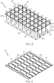
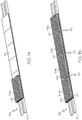
- Structural antenna array 100 includes wall sections 102 (e.g., a plurality of wall sections 102) interconnected to form core 104.
- core 104 may be a honeycomb core or grid-like core formed by approximately parallel (e.g., longitudinal) rows 106 of wall sections 102 approximately perpendicularly interconnected with approximately parallel (e.g., lateral) columns 108 of wall sections 102.
- core 104 of structural antenna array 100 may include ten rows 106 of longitudinally extending wall sections 102 and sixty-one columns 108 of laterally extending wall sections 102.
- Other numbers of wall sections 102 are also contemplated.
- Figs. 1 and 3 illustrate an X-Y grid-like arrangement of wall sections 102 forming core 104 having approximately square shaped openings (e.g., square antenna cells 128)
- a honeycomb or grid-like core 104 having hexagonally shaped openings may also be formed by interconnecting wall sections 102.
- the approximately perpendicular layout of wall sections 102 that form core 104 of structural antenna array 100 is intended to show one implementation of the grid-like layout of wall sections 102 and/or antenna elements 110 and feed elements 126 ( Figs. 3-5 ).
- the type of grid-like layout selected and the overall size of structural antenna array 100 may depend on a particular application with which structural antenna array 100 will be used.
- structural antenna array 100 includes frame 112.
- Frame 112 fits around and supports core 104.
- core 104 fits between opposed (e.g., upper and lower, front and rear, etc.) flanges 118 of frame 112.
- Frame 112 stiffens core 104 and maintains a proper alignment of wall sections 102 (e.g., perpendicular alignment) and a proper shape (e.g., squareness) of core 104 and/or antenna cells 128.
- Frame 112 also provides attachment points for attachment of structural antenna array 100 to a structural portion of the mobile platform.
- Structural antenna array 100 includes first (e.g., front) skin 114 ( Fig. 1 ) and second (e.g., back) skin 116 ( Fig. 2 ).
- First skin 114 (a portion of which has been cut away in Fig. 1 to better illustrate the grid-like arrangement of wall sections 102 forming core 104) and second skin 116 are coupled to core 104 (and distribution substrate layer 190) (not illustrated in Figs. 1 and 2 ) to form a sandwich structure.
- structural antenna array 100 includes a layered structure formed by second skin 116, core 104, distribution substrate layer 190 ( Figs. 9 and 10 ), and first skin 114.
- Structural antenna array 100 may provide sufficient structural strength to be capable of replacing a load bearing structure or structural member.
- structural antenna array 100 may be used as a primary structural component in an aircraft, spacecraft, rotorcraft, or the like. Other possible applications may include use as a primary structural component in marine or land vehicles. Since structural antenna array 100 may be integrated into the structure of the mobile platform, it may not negatively impact the aerodynamics of the mobile platform as much as would be the case with an antenna or antenna array that is required to be mounted on an external surface of an otherwise highly aerodynamic, high speed mobile platform.
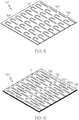
- each one of wall sections 102 includes antenna elements 110 (e.g., a plurality of antenna elements 110) ( Fig. 4 ) and feed elements 126 (e.g., a plurality of feed elements 126) ( Fig. 5 ).
- Antenna elements 110 and feed elements 126 are embedded, integrated, attached, or otherwise formed on opposed surfaces of wall sections 102.
- structural antenna array 100 includes antenna cells 128 (e.g., a plurality of antenna cells 128) ( Fig. 1 ).
- Antenna cells 128 are formed by interconnected wall sections 102, for example, arranged to form the grid-like (e.g., square cell) core 104.
- Core 104 of structural antenna array 100 includes rows 106 and columns 108 of antenna cells 128.
- Antenna elements 110 may be flat (e.g., planar) conductive elements or microstrip antennas. As one example, antenna elements 110 are dipole antenna elements. As one non-limiting example, each one of antenna elements 110 (also referred to herein as antenna element 110) may be configured to operate in a frequency range of between approximately 2 GHz and approximately 4 GHz.
- the perpendicular arrangement of wall sections 102 creates sets of orthogonal dipole antenna elements 110 to provide dual polarization. For example, certain ones of antenna elements 110 are horizontally polarized and certain other ones of antenna elements 110 (e.g., orthogonally oriented) are vertically polarized. In other examples, structural antenna array 100 may include only one set of dipole antenna elements 110 to provide single polarization.
- structural antenna array 100 does not require the use of metallic substrates for supporting antenna elements 110 and/or feed elements 126. Structural antenna array 100 therefore may not have an undesirable parasitic weight penalty.
- parasitic generally means weight that is associated with components of an antenna or an antenna array that are not directly necessary for transmitting or receiving operations.
- structural antenna array 100 is a lightweight structure making it particularly well-suited and beneficial for aerospace applications.
- substrate layer 120 is formed with antenna elements 110 on first surface 122 ( Fig. 4 ) and feed elements 126 on second surface 124 ( Fig. 5 ).
- antenna elements 110 are formed in approximately parallel rows on first surface 122 of substrate layer 120 and feed elements 126 are formed in approximately parallel rows on second surface 124 of substrate layer 120.
- Other arrangements of antenna elements 110 and/or feed elements 126 are also contemplated.
- Each pair of antenna elements 110 (also identified herein as antenna element pair 110a) ( Fig. 4 ) on first surface 122 is associated with one of feed elements 126 (also identified herein as feed element 126) on the opposed second surface 124.
- substrate layer 120 includes a non-conductive substrate material.
- substrate layer 120 may be a printed circuit board ("PCB") material or similar electronic circuit board material (generally referred to herein as electronic board material 192).
- substrate layer 120 may be a glass-reinforced epoxy laminate (also generally known as FR-4).
- substrate layer 120 may be I-Tera® RF MT laminate commercially available from Isola Group, Chandler, Arizona.
- First surface 122 and second surface 124 of substrate layer 120 are each coated with a copper foil (not explicitly illustrated) that is etched away to form antenna elements 110 on first surface 122 and feed elements 126 on second surface 124 having desired dimensions and relative spacing.
- a protective coating (not explicitly illustrated) may be applied to first surface 122 over antenna elements 110 and to second surface 124 over feed elements 126 to protect the copper foil forming antenna elements 110 and feed elements 126.
- the protective coating may be a non-conductive coating, such as a solder mask.
- Antenna elements 110 and feed elements 126 shown with broken lines in Figs. 3 , 6 , 7, 8A , 8B, 8C and 10 to illustrate antenna elements 110 and feed elements 126 covered by protective coating.
- feed elements 126 on second surface 124 of substrate layer 120 are shown with broken lines in Figs. 8A and 10 to illustrate feed elements 126 covered (e.g., hidden) by protective coating and antenna elements 110 on first surface 122 of substrate layer 120 are shown with broken lines in Figs. 8A and 10 to illustrate antenna elements 110 on the non-visible first surface 122 (e.g., hidden behind second surface 124).
- a portion of one or more (e.g., each) antenna elements 110 and one or more (e.g., each) feed element 126 may be exposed (e.g., a portion of the copper foil not covered by the protective coating) to form test contact 160.
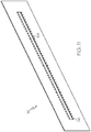
- assembly wall slots 130 are formed into substrate layer 120 at spaced apart locations.
- Each one of wall slots 130 (also identified herein as wall slot 130) includes first (e.g., upper) portion 130a and second (e.g., lower) portion 130b.
- Wall slots 130 facilitate intersecting assembly of wall sections 102 to form core 104 ( Fig. 3 ).
- wall slots 130 may be water jet cut or machine routed into substrate layer 120 to penetrate through an entire thickness of substrate layer 120.
- substrate layer 120 may be cut into a plurality of sections or strips that form wall sections 102.
- one or more wall sections 102 may be cut to an appropriate length (e.g., to shorten the length of wall section 102).
- Height H2 of wall section 102 represents the overall height HI ( Fig. 3 ) of core 104 of structural antenna array 100.
- each wall section 102 is cut to form notches 132 between terminal ends of adjacent feed elements 126 and antenna elements 110.
- Notches 132 enable a terminal end of each feed element 126 to form first (e.g., signal) connector pin 134 (e.g., a first conductive foot) and a terminal end of each antenna element to form second (e.g., ground) connector pin 136 (e.g., a second conductive foot).
- first connector pin 134 and second connector pin 136 may be plated with a conductive material (e.g., covered with copper).
- pairs of antenna elements 110 may be directly (e.g., physically) coupled together (e.g., formed from a continuous strip of the copper material).
- Antenna element 110 of one antenna element pair 110a that is adjacent to antenna element 110 of another antenna element pair 110a may be capacitively coupled together.
- capacitive coupling pad 188 may be coupled to second surface 124 (e.g., physically and electrically coupled to electronic board material 192). Capacitive coupling pad 188 may facilitate and enable capacitive connection and communication between antenna elements 110.
- antenna elements 110 and feed elements 126 may be directly coupled (e.g., physically and electrically connected) together via connection to distribution substrate layer 190 ( Fig. 10 ). In one example, antenna elements 110 and feed elements 126 may be capacitively coupled together (e.g., through the thickness of substrate layer 120) via capacitive coupling pad 188.
- first skin 114 and second skin 116 include multiple substrate material layers forming a sandwich structure (also referred to as a superstrate).
- first skin 114 includes first (e.g., inner) non-conductive substrate layer 140, second (e.g., outer) substrate layer 142, and a dielectric substrate layer 144 disposed between first non-conductive substrate layer 140 and second non-conductive substrate layer 142.
- first skin 114 includes first (e.g., inner) non-conductive substrate layer 146, second (e.g., outer) substrate layer 148, and dielectric substrate layer 150 disposed between first non-conductive substrate layer 146 and second non-conductive substrate layer 148.
- first non-conductive substrate layer 140 and second substrate layer 142 of first skin 114 and first non-conductive substrate layer 146 and second substrate layer 148 of second skin 116 may be electronic board material 192 (e.g., a PCB material or similar electronic circuit board material).
- first non-conductive substrate layer 140, second substrate layer 142, first non-conductive substrate layer 146, and second substrate layer 148 may be a glass-reinforced epoxy laminate (also generally known as FR-4).
- first non-conductive substrate layer 140, second substrate layer 142, first non-conductive substrate layer 146, and second substrate layer 148 may be I-Tera® RF MT laminate.
- first non-conductive substrate layer 140 and second substrate layer 142 of first skin 114 and/or first non-conductive substrate layer 146 and second substrate layer 148 of second skin 116 may include multiple plies (e.g., five plies) of I-Tera® RF MT that are cured to form a laminate structure.
- dielectric substrate layer 144 of first skin 114 and dielectric substrate layer 150 of second skin 116 may be any suitable dielectric material that is an electrical insulator and allows electromagnetic waves (e.g., radio frequency ("RF") waves) to propagate through the material.
- dielectric substrate layer 144 and dielectric substrate layer 150 may be a dielectric foam material.
- dielectric substrate layer 144 and dielectric substrate layer 150 may be Eccostock® Lok commercially available from Emerson & Cuming Microwave Products, Inc., Randolph, Massachusetts.
- dielectric substrate layer 144 of first skin 114 and dielectric substrate layer 150 of second skin 116 may include a sheet of Eccostock® Lok approximately 0.25 inch thick.
- dielectric constant the dielectric material of dielectric substrate layer 144 and/or dielectric substrate layer 150 may depend on (e.g., be selected based on) various antenna parameters including, but not limited to, operating frequency, bandwidth, and the like.
- first skin 114 and second skin 116 illustrated in Fig. 10 include three substrate layers (e.g., inner and outer non-conductive substrate layers and a dielectric substrate layer) other configurations or arrangements of substrate layers are also contemplated.
- first skin 114 and/or second skin 116 may include one or more additional non-conductive substrate layers disposed between the inner and outer non-conductive substrate layers.
- First skin 114 and second skin 116 provide structural stiffness to structural antenna array 100.
- the dielectric material of dielectric substrate layer 144 of first skin 114 and dielectric substrate layer 150 of second skin 116 may be chosen to appropriately tune the RF transmission and reception capabilities of structural antenna array 100 (e.g., of antenna elements 110).
- the dielectric material of dielectric substrate layer 144 of first skin 114 and dielectric substrate layer 150 of second skin 116 may be selected to suitably work with the attenuation of antenna elements 110.
- the dielectric properties of dielectric substrate layer 144 of first skin 114 and dielectric substrate layer 150 of second skin 116 may be the same.
- the dielectric properties of dielectric substrate layer 144 of first skin 114 and dielectric substrate layer 150 of second skin 116 may be different to tune structural antenna array 100.
- a thickness of dielectric substrate layer 144 and/or dielectric substrate layer 150 may be modified based on particular performance parameters.
- structural antenna array 100 includes distribution substrate layer 190 (e.g., an electronic distribution board).
- Core 104 e.g., each one of interconnected wall sections 102 may be mechanically and electrically coupled to distribution substrate layer 190.
- distribution substrate layer 190 is disposed between core 104 and second skin 116.
- distribution substrate layer 190 includes a non-conductive substrate material.
- distribution substrate layer 190 may be electronic board material 192 (e.g., a PCB material or similar electronic circuit board material).
- distribution substrate layer 190 may be a glass-reinforced epoxy laminate (also generally known as FR-4).
- distribution substrate layer 190 may be I-Tera® RF MT laminate.
- distribution substrate layer 190 may include multiple plies (e.g., five plies) of I-Tera® RF MT that are cured to form a laminate structure.
- distribution substrate layer 190 includes vias 138.
- Vias 138 are holes formed at least partially through the thickness of distribution substrate layer 190.
- First connector pins 134 and second connector pins 136 of wall sections 102 are inserted into vias 138 to mechanically couple wall sections 102 to distribution substrate layer 190 (e.g., to mechanically couple core 104 to distribution substrate layer 190).
- Vias 138 may be plated with a conductive material (e.g., covered with copper) to electrically couple feed elements 126 to distribution substrate layer 190.
- Vias 138 are electrically interconnected throughout distribution substrate layer 190 by a plurality of conductive tracks or traces (not explicitly illustrated) extending throughout distribution substrate layer 190.
- distribution substrate layer 190 electrically interconnects antenna elements 110 and feed elements 126 together and to radio transceiver electronics (not explicitly illustrated), for example, of the mobile platform.
- radio frequency (“RF") connectors 152 are mechanically and electrically coupled to distribution substrate layer 190.
- RF connectors 152 may be any suitable RF connector, such as a coaxial RF connector.
- RF connectors 152 are mechanically and electrically coupled to vias 138 formed in distribution substrate layer 190. RF connectors 152 are electrically coupled to feed elements 126 and/or antenna elements 110 by the plurality of conductive tracks or traces extending throughout distribution substrate layer 190.
- distribution substrate layer 190 serves as an electronics distribution vehicle that integrates feed elements 126 and antenna elements 110 of wall sections 102.
- antenna elements 110 and feed elements 126 are physically connected to RF connectors 152 by distribution substrate layer 190.
- Structural antenna array 100 may be coupled to the radio transceiver electronics (not explicitly illustrated) of the mobile platform by RF connectors 152.
- a portion of feed elements 126 (e.g., a selected plurality of feed elements 126) and/or a portion of antenna elements 110 (e.g., a selected plurality of antenna elements 110) are coupled to and associated with pairs of RF connectors 152.
- feed elements 126 and/or antenna elements 110 of at least one column 108 of antenna cells 128 are associated with two RF connectors 152.
- One of the two RF connectors 152 may be associated with horizontally polarized antenna elements 110 and another one of the two RF connectors 152 may be associated with vertical polarized antenna elements 110.
- structural antenna array 100 operates in a wide band (e.g., S-band) frequency range, for example, between approximately 2 GHz and approximately 4 GHz.
- Structural antenna array 100 is also dual polarized (e.g., is horizontally and vertically polarized).
- skin slot 158 is formed in second skin 116.
- skin slot 158 may be water cut or machine routed at least into second skin 116 (e.g., at least partially through second non-conductive substrate layer 148 and dielectric substrate layer 150).
- Skin slot 158 facilitates access to RF connectors 152 ( Figs. 2 and 9 ) that are connected to distribution substrate layer 190.
- RF connectors 152 are aligned within and extend at least partially through skin slot 158.
- connector support 154 may be fit within skin slot 158 and coupled to second skin 116.
- Connector support 154 may support and reinforce RF connectors 152.
- connector support 154 is a rigid plate, for example, made of metal, having a plurality of holes (not explicitly illustrated) that are suitably sized and shaped to receive RF connectors 152.
- threaded inserts 156 may be installed in second skin 116 to facilitate connection of connector support 154.
- holes may be formed (e.g., machined) at least partially through second non-conductive substrate layer 148 and dielectric substrate layer 150 of second skin 116 along side of skin slot 158. Threaded inserts 156 may be installed within the formed holes.
- a potting compound (not explicitly illustrated) may be used to bond threaded inserts 156 within second skin 116.
- Fasteners (not explicitly illustrated) may be connected to threaded inserts 156 for connection of connector support 154 to second skin 116.
- core 104 may be made of or formed from a plurality of core sections or core portions connected together.
- one or more wall sections 102 may include two or more wall portions connected together.
- at least one wall section 102 includes first wall portion 162a and second wall portion 162b. Adjacent edges (not explicitly identified) of first wall portion 162a and second wall portion 162b are abutted together to form wall section 102.
- Conductive splice 164 may be used to electrically connect one of antenna elements 110 (e.g., half of antenna element 110a) of first wall portion 162a and to an adjacent one of antenna elements 110 (e.g., half of adjacent antenna element 110b) of second wall portion 162b.
- Conductive splice 164 may be made of any appropriate conductive material. As non-limiting examples, conductive splice 164 may be made of solder, foil, conductive adhesive, conductive mesh, or the like.
- Non-conductive splice clip 166 may be made of a structural non-conductive material.
- non-conductive splice clip 166 may be made of electronic board material 190 (e.g., PCB or other suitable electronic circuit board material).
- non-conductive splice clip 166 may be a glass-reinforced epoxy laminate (also generally known as FR-4).
- non-conductive splice clip 166 may be I-Tera® RF MT laminate.
- Non-conductive splice clip 166 may be attached to wall section 102 (e.g., between first wall portion 162a and second wall portion 162b) over conductive splice 164.
- Non-conductive splice clip 166 may be attached to wall section 102 using a suitable non-conductive adhesive or other bonding agent.
- Non-conductive splice clip 166 is designed to not interfere with any exposed conductive material of wall section 102 (e.g., copper foil or other electronic pads).
- structural antenna array 100 overcomes numerous disadvantages present in conventional structural antenna arrays including producability, expense, size and weight limitations, and RF performance.
- the use of electronic board material 190 to make wall sections 102, distribution substrate layer 190, first non-conductive substrate layer 146 and second non-conductive substrate layer 148 of second skin 116, and first non-conductive substrate layer 140 and second non-conductive substrate layer 142 of first skin 114 may eliminate producability issues arising due to mismatches of coefficient of thermal expansion between materials and reduce production costs.
- Second skin 116 and first skin 114 bonded to core 104 (and distribution substrate layer 190) produces a lightweight and strong structural member that can be integrated into another structure. Structural integration of structural antenna array 100 into a structural member of a mobile platform enables a significant increase in antenna aperture size over conventional antenna arrays.
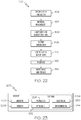
- Method 200 is one example implementation of the disclosed method for making structural antenna array 100. Modifications, additions, or omissions may be made to method 200 without departing from the scope of the present disclosure. Method 200 may include more, fewer, or other steps. Additionally, steps may be performed in any suitable order.
- method 200 includes the step of forming core 104 including intersecting wall sections 102, as shown at block 302.
- Wall sections 102 include electronic board material 190 having antenna elements 110 on first surface 122, feed elements 126 on second surface 124, and connector pins 134, 136 extending from an edge of wall sections 102 and coupled to feed elements 126 and antenna elements 110.
- wall sections 102 are perpendicularly interconnected, for example, by mating first portions 130a and second portions 130b of wall slots 130 to form rows 106 and columns 108 of antenna cells 128.
- Each one of antenna cells 128 (also referred to as antenna cell 128) includes an orthogonally oriented pair of antenna elements 110 (e.g., antenna element pair 110a) and an associated pair of feed elements 126 capacitively coupled to the pair of antenna elements 110.
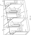
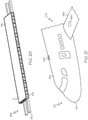
- tooling 168 may be used to construct structural antenna array 100.
- tooling 168 may include first support member 170 (e.g., a connected pair of tubing, channel, etc.) suitably sized and shaped to support structural antenna array 100.
- Tooling 168 may also include one or more support plates 172 positioned on first support member 170.
- Support plates 172 may be made of a material having similar thermal expansion properties (e.g., having a matching coefficient of thermal expansion) as that of wall sections 102, second skin 116 and first skin 114.
- support plates 172 may be a glass-reinforced epoxy laminate (e.g., FR-4).
- Core 104 may be constructed by interconnecting wall sections 102 on tooling 168 (e.g., on first support member 170 and support plates 172). As illustrated in Fig. 15 , depending upon the overall length L1 ( Fig. 1 ) of structural antenna array 100 and the length L2 ( Fig. 7 ) of wall sections 102, core 104 may include a plurality of core sections (identified individually as first core section 104a, second core section 104b, third core section 104c, and fourth core section 104d). In such an example, adjacent wall sections 102 may be joined at splice locations 174 to form the longitudinal rows of wall sections 102. Joining adjacent wall section 102 (e.g., first wall portion 162a and second wall portion 162b) may be performed as described above and with reference to Fig. 12 .
- Joining adjacent wall section 102 e.g., first wall portion 162a and second wall portion 162b
- Joining adjacent wall section 102 may be performed as described above and with reference to Fig. 12
- method 200 includes the step of connecting frame 112 around core 104, as shown at block 304.
- method 200 includes the step of positioning distribution substrate layer 190 on core 104, as shown at block 306.
- distribution substrate layer 190 ( Fig. 10 ) of is positioned on core 104 such that vias 138 ( Fig. 10 ) formed in distribution substrate layer 190 are aligned with first connector pins 134 and second connector pins 136 extending from the edge of wall sections 102.
- Method 200 also includes the step of connecting connector pins 134, 136 to vias 138, as shown at block 308. Connecting (e.g., inserting) connector pins 134, 136 to vias 138 mechanically couples wall sections 102 to distribution substrate layer 190.
- Method 200 also includes the step of soldering connector pins 134, 136 to vias 138, as shown at block 310. Soldering connector pins 134, 136 to vias 138 electrically coupled feed elements 126 to distribution substrate layer 190.
- distribution substrate layer 190 may be constructed from a plurality of distribution substrate layer sections (not explicitly illustrated).
- each distribution substrate layer section may include a section of distribution substrate layer 190.
- Each distribution substrate layer section may be spliced together (e.g., mechanically and electrically).
- method 200 also includes the step of connecting RF connectors 152 to distribution substrate layer 190, as shown at block 312. Connecting RF connectors 152 to distribution substrate layer 190 electrically couples RF connectors 152 to feed elements 126 and/or antenna elements 110. As one example, RF connectors 152 may be connected (e.g., inserted and soldered) to vias 138 in first non-conductive substrate layer 146.
- method 200 includes the step of testing continuity of structural antenna array 110, as shown at block 322.
- core 104 e.g., wall sections 102
- the electrical continuity of structural antenna array 110 may be tested using test contacts 160 of antenna elements 110 and/or feed elements 126 formed on wall sections 102.
- the ability to test the continuity and to verify proper function and operation of the electronic components (e.g., antenna elements 110, feed elements 126, RF connectors 152) of structural antenna array 100 prior to completion of construction (e.g., prior to application of a structural adhesive and/or connection of second skin 116 and/or first skin 114) beneficially allows repairs to be performed on structural antenna array 100.
- method 200 includes the step of applying a structural adhesive (not explicitly illustrated) to core 104 and/or distribution substrate layer 190, as shown at block 314.
- the structural adhesive may be poured or sprayed onto core 104 and distribution substrate layer 190 and within each one of antenna cells 128 ( Fig. 3 ).
- the structural adhesive may be a resin material suitable to structurally stabilize (e.g., bond) interconnecting edges of wall sections 102 to one another and wall sections 102 to distribution substrate layer 190.
- tooling 168 may also include second support member 176.
- second support member 176 e.g., a connected pair of tubing, channel, etc.
- second support member 176 may be suitably sized and shaped to support structural antenna array 100 and clamp structural antenna array 100 between first support member 170 and second support member 176, for example, to rotate structural antenna array 100 about axis of rotation R, during construction.
- Additional support plates 172 may be positioned between structural antenna array 100 and second support member 176.
- a partially constructed structural antenna array 100 (e.g., distribution substrate layer 190 and core 104) may be clamped between first support member 170 and second support member 176, rotated 180 degrees, and first support member 170 removed, for example, to expose antenna cells 128 and application of application of the structural adhesive to core 104 (e.g., wall sections 102) and distribution substrate layer 190 (block 314), as illustrated in Fig. 19 .
- method 200 includes the step of positioning first skin 114 on core 104, as shown at block 316.
- First skin 114 is positioned opposite distribution substrate layer 190.
- First skin 114 may be formed layer-by-layer.
- first non-conductive substrate layer 140 ( Fig. 10 ) of first skin 114 is positioned on core 104.
- Dielectric substrate layer 144 ( Fig. 10 ) of first skin 114 is positioned on first non-conductive substrate layer 140.
- Second non-conductive substrate layer 142 of first skin 114 is positioned on dielectric substrate layer 144.
- first skin 114 may also include at least one adhesive layer, such as Metalbond® 1515-3 film adhesive, disposed between first non-conductive substrate layer 140 and dielectric substrate layer 144 and between dielectric substrate layer 144 and second non-conductive substrate layer 142.
- at least one adhesive layer may be disposed between first skin 114 (e.g., first non-conductive substrate layer 140) and core 104. The adhesive layers bond first non-conductive substrate layer 140, dielectric substrate layer 144, second non-conductive substrate layer 142, and core 104 together, for example, during a curing operation.
- first skin 114 may be constructed from a plurality of second skin sections (not explicitly illustrated).
- each second skin section may include a section of first non-conductive substrate layer 140, a section of dielectric substrate layer 144, and a section of second non-conductive substrate layer 142.
- Each second skin section may be spliced together.
- first support member 170 and support plates 172 may be positioned on first skin 114 to clamp structural antenna array 100 between second support member 176 (and support plates 172) and first support member 170 (and support plates 172) and rotated 180 degrees for positioning of second skin 116. Second support member 176 and support plates 172 may be removed following rotation, as illustrated in Fig. 24 .
- method 200 includes the step of positioning second skin 116 on distribution substrate layer 190, as shown at block 324.
- Second skin 116 may be positioned opposite first skin 114 to form the sandwich structure of second skin 116, core 104, distribution substrate layer 190, and first skin 114, as best illustrated in Fig. 10 .
- Second skin 116 may be formed layer-by-layer on distribution substrate layer 190.
- first non-conductive substrate layer 146 ( Fig. 10 ) of second skin 116 is positioned on distribution substrate layer 190.
- Dielectric substrate layer 150 ( Fig. 10 ) of second skin 116 is positioned on first non-conductive substrate layer 146.
- Second non-conductive substrate layer 148 of second skin 116 is positioned on dielectric substrate layer 150. While not explicitly illustrated, second skin 116 may also include at least one adhesive layer, such as Metalbond® 1515-3 film adhesive commercially available from Cytec Industries, Inc., Woodland Park, New Jersey, disposed between first non-conductive substrate layer 146 and dielectric substrate layer 150 and between dielectric substrate layer 150 and second non-conductive substrate layer 148. Similarly, at least one adhesive layer may be disposed between second skin 116 (e.g., first non-conductive substrate layer 146) and distribution substrate layer 190. The adhesive layers bond first non-conductive substrate layer 146, dielectric substrate layer 150, second non-conductive substrate layer 148, and distribution substrate layer 190 together, for example, during a curing operation.
- adhesive layer such as Metalbond® 1515-3 film adhesive commercially available from Cytec Industries, Inc., Woodland Park, New Jersey
- second skin 116 may be constructed from a plurality of first skin sections (not explicitly illustrated).
- each first skin section may include a section of first non-conductive substrate layer 146, a section of dielectric substrate layer 150, and a section of second non-conductive substrate layer 148.
- Each first skin section may be spliced together.
- first skin 114 may be positioned on core 104 after second skin 116 is positioned on distribution substrate layer 190.
- second skin 116 may be positioned on distribution substrate layer 190 before rotation and application of the structural adhesive (block 314), and then first skin 114 may be positioned on core 104.
- second skin 116 may be positioned on distribution substrate layer 190 following application of the structural adhesive and rotation.
- RF connectors 152 may extend through skin slot 158 formed in second skin 116 (e.g., formed through dielectric substrate layer 150 and second non-conductive substrate layer 148).
- method 200 includes the step of curing structural antenna array 100 (e.g., the assembled combination of second skin 116, core 104, and first skin 114), as shown at block 318.
- Curing structural antenna array 100 may include heating second skin 116, core 104, distribution substrate layer 190, and first skin 114 to an appropriate temperature for an appropriate period of time, for example, in an oven.
- structural antenna array 100 may be cured at a temperature of approximately 250 °F for 120 minutes.
- method 200 includes the step of attaching connector support 154 to second skin 116, as shown at block 320.
- the disclosed structural antenna array 100 is integrated within and forms a portion of structural member 178 of mobile platform 180.
- Structural member 178 may include any suitable primary structure of mobile platform 180.
- structural antenna array 100 may form a part of at least one of fuselage 184 or wing 186 of aircraft 182.
- Aircraft 1200 may be one example of mobile platform 180 (e.g., aircraft 182) ( Fig. 21 ).
- Aircraft applications of the disclosed examples of structural antenna array 100 may include, for example and without limitation, composite stiffened members such as fuselage skins, wing skins, control surfaces, hatches, floor panels, door panels, access panels, empennages, and the like.
- the illustrative method 1100 may include specification and design, as shown at block 1102, of aircraft 1200, which may include design of structural antenna array 100 for a particular antenna capability, and material procurement, as shown at block 1104.
- component and subassembly manufacturing as shown at block 1106, and system integration, as shown at block 1108, of aircraft 1200 may take place.
- Fabrication of structural antenna array 100 as described herein may be accomplished as a portion of the production, component and subassembly manufacturing step (block 1106) and/or as a portion of the system integration (block 1108).
- aircraft 1200 may go through certification and delivery, as shown block 1110, to be placed in service, as shown at block 1112.
- aircraft 1200 While in service, aircraft 1200 may be scheduled for routine maintenance and service, as shown at block 1114.
- Routine maintenance and service may include modification, reconfiguration, refurbishment, etc. of one or more systems of aircraft 1200.
- Structural antenna array 100 may also be used during routine maintenance and service (block 1114).
- a system integrator may include, without limitation, any number of aircraft manufacturers and major-system subcontractors; a third party may include, without limitation, any number of vendors, subcontractors, and suppliers; and an operator may be an airline, leasing company, military entity, service organization, and so on.
- aircraft 1200 produced by illustrative method 1100 may include airframe 1202 having one or more structurally integrated structural antenna arrays 100, and a plurality of high-level systems 1204 and interior 1206.
- high-level systems 1204 include one or more of propulsion system 1208, electrical system 1210, hydraulic system 1212 and environmental system 1214. Any number of other systems may be included.
- propulsion system 1208 electrical system 1210, hydraulic system 1212 and environmental system 1214. Any number of other systems may be included.
- an aerospace example is shown, the principles disclosed herein may be applied to other industries, such as the automotive industry, the marine industry, and the like.
- components or subassemblies corresponding to component and subassembly manufacturing may be fabricated or manufactured in a manner similar to components or subassemblies produced while aircraft 1200 is in service (block 1112).
- one or more examples of the apparatus and methods, or combination thereof may be utilized during production stages (blocks 1108 and 1110).
- one or more examples of the systems, apparatus, and methods, or a combination thereof may be utilized, for example and without limitation, while aircraft 1200 is in service (block 1112) and during maintenance and service stage (block 1114).
Landscapes
- Engineering & Computer Science (AREA)
- Physics & Mathematics (AREA)
- Astronomy & Astrophysics (AREA)
- Aviation & Aerospace Engineering (AREA)
- General Physics & Mathematics (AREA)
- Remote Sensing (AREA)
- Manufacturing & Machinery (AREA)
- Variable-Direction Aerials And Aerial Arrays (AREA)
- Details Of Aerials (AREA)
- Support Of Aerials (AREA)
Claims (15)
- Réseau d'antennes structurel (100) comprenant :un noyau (104) comprenant des sections de paroi se croisant (102), dans lequel ledit noyau (104) comprend en outre des éléments d'antenne (110) formés sur une première surface (122) desdites sections de paroi (102), et des éléments d'alimentation (126) formés sur une seconde surface opposée (124) desdites sections de paroi (102), dans lequel une extrémité terminale de chacun des éléments d'alimentation (126) comprend une première broche de connecteur respective (134) s'étendant à partir d'un bord desdites sections de paroi (102) et une extrémité terminale de chacun des éléments d'antenne (110) comprend une seconde broche de connecteur respective (136) s'étendant à partir d'un bord desdites sections de paroi (102), dans lequel un bord de chacune desdites sections de paroi (102) est découpé pour former des encoches (132) entre des extrémités terminales d'éléments d'alimentation adjacents (126) et des éléments d'antenne (110) et dans lequel les encoches (132) permettent à une extrémité terminale de chacun des éléments d'alimentation (126) de former les premières broches de connecteur respectives (134) et à une extrémité terminale de chacun des éléments d'antenne (110) de former les secondes broches de connecteur respectives (136) ;une couche de substrat de distribution (190) comprenant une pluralité de trous d'interconnexion (138), dans lequel les premières broches de connecteur (134) et les secondes broches de connecteur (136) des sections de paroi (102) sont insérées dans certains respectifs parmi les trous d'interconnexion (138) pour coupler mécaniquement les sections de paroi (102) à la couche de substrat de distribution (190), dans lequel les trous d'interconnexion (138) couplent électriquement les éléments d'alimentation (126) à la couche de substrat de distribution (190) et la couche de substrat de distribution (190) est en communication électrique avec lesdits éléments d'antenne (110) et lesdits éléments d'alimentation (126) ;une pluralité de connecteurs RF (152) couplés à et en communication électrique avec ladite couche de substrat de distribution (190) et couplés électriquement aux éléments d'alimentation (126) et aux éléments d'antenne (110) ;une première peau (114) couplée audit noyau (104) à l'opposé de ladite couche de substrat de distribution (190) ; etune seconde peau (116) couplée à ladite couche de substrat de distribution (190) opposée à ladite première peau (114) .
- Réseau d'antennes structurel (100) selon la revendication 1, dans lequel lesdits éléments d'antenne (110) comprennent des éléments d'antenne dipôle.
- Réseau d'antennes structurel (100) selon les revendications 1 ou 2, dans lequel ledit noyau (104) comprend une structure de cellule carrée desdites sections de paroi (102) se croisant perpendiculairement pour former des colonnes et des rangées de cellules d'antenne (128).
- Réseau d'antennes structurel (100) selon la revendication 3, dans lequel chacune desdites cellules d'antenne (128) comprend au moins une paire desdits éléments d'antenne (110) orientés orthogonalement pour fournir une polarisation double.
- Réseau d'antennes structurel (100) selon l'une quelconque des revendications 1 à 4, dans lequel chacune desdites sections de paroi (102) comprend un matériau de carte électronique (192).
- Réseau d'antennes structurel (100) selon l'une quelconque des revendications 1 à 5, dans lequel ladite couche de substrat de distribution (190) comprend un matériau de carte électronique (192).
- Réseau d'antennes structurel (100) selon l'une quelconque des revendications 1 à 6, dans lequel ladite première peau (114) et ladite seconde peau (116) comprennent chacune :une première couche de substrat non conductrice ;une couche de substrat diélectrique couplée à ladite première couche de substrat non conductrice ; etune seconde couche de substrat non conductrice couplée à ladite couche de substrat diélectrique opposée à ladite première couche de substrat non conductrice.
- Réseau d'antennes structurel (100) selon la revendication 1, dans lequel des paires desdits connecteurs RF (152) sont en communication électrique avec certains sélectionnés desdits éléments d'alimentation (126) et certains sélectionnés desdits éléments d'antenne (110).
- Réseau d'antennes structurel (100) selon l'une quelconque des revendications 1 à 8, dans lequel au moins l'une desdites sections de paroi (102) comprend une première partie de paroi (162a), une seconde partie de paroi (162b) et une épissure conductrice connectant électriquement l'un desdits éléments d'antenne (110) de ladite première partie de paroi (162a) à l'un adjacent desdits éléments d'antenne (110) de ladite seconde partie de paroi (162b).
- Réseau d'antennes structurel (100) selon la revendication 9, comprenant en outre une attache d'épissure non conductrice (164) connectée à ladite première partie de paroi (162a) et à ladite seconde partie de paroi (162b) au-dessus de ladite épissure conductrice (164).
- Procédé de fabrication d'un réseau d'antennes structurel (100) comprenant les étapes consistant à :former un noyau (104) comprenant des sections de paroi se croisant (102), dans lequel lesdites sections de paroi (102) comprennent des éléments d'antenne (110) formés sur une première surface (122), des éléments d'alimentation (126) formés sur une seconde surface opposée (124), dans lequel une extrémité terminale de chacun des éléments d'alimentation (126) comprend une première broche de connecteur respective (134) s'étendant à partir d'un bord desdites sections de paroi (102) et une extrémité terminale de chacun des éléments d'antenne (110) comprend une seconde broche de connecteur respective (136) s'étendant à partir d'un bord desdites sections de paroi (102), dans lequel un bord de chacune desdites sections de paroi (102) est découpé pour former des encoches (132) entre des extrémités terminales d'éléments d'alimentation adjacents (126) et d'éléments d'antenne (110) et dans lequel les encoches (132) permettent à une extrémité terminale de chacun des éléments d'alimentation (126) de former des premières broches de connecteur respectives (134) et une extrémité terminale de chacun des éléments d'antenne (110) de former les secondes broches de connecteur respectives (136) ;connecter un cadre autour dudit noyau (104) ;positionner une couche de substrat de distribution (190) sur ledit noyau (104), dans lequel ladite couche de substrat de distribution (190) comprend une pluralité de trous d'interconnexion ;connecter lesdites premières broches de connecteur (134) et lesdites secondes broches de connecteur (136) à certains respectifs parmi lesdits trous d'interconnexion pour coupler mécaniquement lesdites sections de paroi (102) à ladite couche de substrat de distribution (190) ;souder lesdites broches de connecteur auxdits trous d'interconnexion pour coupler électriquement lesdits éléments d'alimentation (126) et lesdits éléments d'antenne (110) à ladite couche de substrat de distribution (190) ;connecter des connecteurs RF à ladite couche de substrat de distribution (190) pour coupler électriquement lesdits éléments d'alimentation (126) et lesdits éléments d'antenne (110) auxdits connecteurs RF ;positionner une première peau (114) sur ledit noyau (104) à l'opposé de ladite couche de substrat de distribution (190) ;positionner une seconde peau (116) sur ladite couche de substrat de distribution (190) à l'opposé de ladite première peau (114) ; etdurcir ledit noyau (104), ladite couche de substrat de distribution (190), ladite première peau (114) et ladite seconde peau (116).
- Procédé selon la revendication 11, comprenant en outre les étapes consistant à :tester une continuité électrique dudit noyau (104) connecté à ladite couche de substrat de distribution (190) ; etappliquer un adhésif structurel audit noyau (104) et à ladite couche de substrat de distribution (190).
- Plate-forme mobile (180) comprenant :un élément structurel (178) ; etun réseau d'antennes structurel (100) selon l'une quelconque des revendications 1 à 10, couplé à et formant une partie dudit élément structurel (178).
- Plate-forme mobile (180) selon la revendication 13, dans laquelle l'élément structurel (178) comprend au moins un parmi un fuselage et une aile d'un aéronef.
- Utilisation d'un réseau d'antennes structurel (100) selon l'une quelconque des revendications 1 à 10 en tant que composant structurel primaire dans un aéronef, un engin spatial, un giravion, un véhicule marin ou un véhicule terrestre.
Applications Claiming Priority (1)
| Application Number | Priority Date | Filing Date | Title |
|---|---|---|---|
| US14/988,869 US10141656B2 (en) | 2016-01-06 | 2016-01-06 | Structural antenna array and method for making the same |
Publications (2)
| Publication Number | Publication Date |
|---|---|
| EP3190657A1 EP3190657A1 (fr) | 2017-07-12 |
| EP3190657B1 true EP3190657B1 (fr) | 2021-06-30 |
Family
ID=57708513
Family Applications (1)
| Application Number | Title | Priority Date | Filing Date |
|---|---|---|---|
| EP17150149.7A Active EP3190657B1 (fr) | 2016-01-06 | 2017-01-03 | Réseau d'antennes structural et son procédé de fabrication |
Country Status (5)
| Country | Link |
|---|---|
| US (1) | US10141656B2 (fr) |
| EP (1) | EP3190657B1 (fr) |
| JP (1) | JP7044466B2 (fr) |
| CN (1) | CN107026307B (fr) |
| RU (1) | RU2716844C2 (fr) |
Families Citing this family (4)
| Publication number | Priority date | Publication date | Assignee | Title |
|---|---|---|---|---|
| RU2692091C1 (ru) * | 2018-06-18 | 2019-06-21 | Российская Федерация, от имени которой выступает Министерство обороны Российской Федерации | Способ построения приёмопередающего модуля активной фазированной антенной решётки |
| US11539118B2 (en) | 2021-01-27 | 2022-12-27 | Rockwell Collins, Inc. | Multi-polarization HF NVIS for vertical lift aircraft |
| US11456537B1 (en) | 2021-01-27 | 2022-09-27 | Rockwell Collins, Inc. | Vertical lift aircraft panels with embedded spiral antennas |
| WO2024044781A1 (fr) * | 2022-08-25 | 2024-02-29 | 3Dfortify Inc. | Superstrats basés sur un réseau diélectrique à faible perte et leurs procédés de production |
Family Cites Families (23)
| Publication number | Priority date | Publication date | Assignee | Title |
|---|---|---|---|---|
| US5786792A (en) * | 1994-06-13 | 1998-07-28 | Northrop Grumman Corporation | Antenna array panel structure |
| US6333712B1 (en) | 1999-11-04 | 2001-12-25 | The Boeing Company | Structural deformation compensation system for large phased-array antennas |
| US6512487B1 (en) | 2000-10-31 | 2003-01-28 | Harris Corporation | Wideband phased array antenna and associated methods |
| US7113142B2 (en) | 2004-10-21 | 2006-09-26 | The Boeing Company | Design and fabrication methodology for a phased array antenna with integrated feed structure-conformal load-bearing concept |
| US7109943B2 (en) * | 2004-10-21 | 2006-09-19 | The Boeing Company | Structurally integrated antenna aperture and fabrication method |
| US7109942B2 (en) | 2004-10-21 | 2006-09-19 | The Boeing Company | Structurally integrated phased array antenna aperture design and fabrication method |
| US7046209B1 (en) * | 2004-10-21 | 2006-05-16 | The Boeing Company | Design and fabrication methodology for a phased array antenna with shielded/integrated feed structure |
| CN1941503B (zh) * | 2005-09-30 | 2011-05-18 | 西北工业大学 | S波段左手材料微带天线 |
| US8446330B1 (en) | 2010-01-26 | 2013-05-21 | The Boeing Company | Antenna fabrication |
| CN101867084A (zh) * | 2010-06-10 | 2010-10-20 | 西北工业大学 | 一种新型嵌入式复合材料智能蒙皮天线结构 |
| US8661649B1 (en) | 2010-10-24 | 2014-03-04 | The Boeing Company | Structurally integrated antenna aperture electronics attachment design and methodology |
| US8643554B1 (en) | 2011-05-25 | 2014-02-04 | The Boeing Company | Ultra wide band antenna element |
| US9368879B1 (en) | 2011-05-25 | 2016-06-14 | The Boeing Company | Ultra wide band antenna element |
| US9099777B1 (en) | 2011-05-25 | 2015-08-04 | The Boeing Company | Ultra wide band antenna element |
| US9072771B1 (en) * | 2011-08-26 | 2015-07-07 | Sti-Co Industries, Inc. | Locomotive antenna arrays |
| US8972310B2 (en) | 2012-03-12 | 2015-03-03 | The Boeing Company | Method for identifying structural deformation |
| US8912975B1 (en) | 2012-09-20 | 2014-12-16 | The Boeing Company | Reworking array structures |
| US9287632B2 (en) | 2012-11-30 | 2016-03-15 | The Boeing Company | Structural wideband multifunctional apertures |
| US9172147B1 (en) | 2013-02-20 | 2015-10-27 | The Boeing Company | Ultra wide band antenna element |
| IL228426B (en) * | 2013-09-15 | 2018-10-31 | Elta Systems Ltd | Temperature control for show array antenna |
| US9190727B1 (en) | 2013-10-01 | 2015-11-17 | The Boeing Company | Structural wideband multifunctional aperture manufacturing |
| US10658758B2 (en) | 2014-04-17 | 2020-05-19 | The Boeing Company | Modular antenna assembly |
| US9735475B2 (en) * | 2014-12-01 | 2017-08-15 | Anderson Contract Engineering, Inc. | Low cost antenna array and methods of manufacture |
-
2016
- 2016-01-06 US US14/988,869 patent/US10141656B2/en active Active
- 2016-09-13 RU RU2016136724A patent/RU2716844C2/ru active
-
2017
- 2017-01-03 EP EP17150149.7A patent/EP3190657B1/fr active Active
- 2017-01-05 JP JP2017000571A patent/JP7044466B2/ja active Active
- 2017-01-05 CN CN201710007313.3A patent/CN107026307B/zh active Active
Non-Patent Citations (1)
| Title |
|---|
| None * |
Also Published As
| Publication number | Publication date |
|---|---|
| US10141656B2 (en) | 2018-11-27 |
| CN107026307B (zh) | 2020-12-22 |
| JP2017171276A (ja) | 2017-09-28 |
| CN107026307A (zh) | 2017-08-08 |
| EP3190657A1 (fr) | 2017-07-12 |
| RU2716844C2 (ru) | 2020-03-17 |
| JP7044466B2 (ja) | 2022-03-30 |
| US20170194715A1 (en) | 2017-07-06 |
| RU2016136724A3 (fr) | 2020-01-13 |
| RU2016136724A (ru) | 2018-03-22 |
Similar Documents
| Publication | Publication Date | Title |
|---|---|---|
| JP4823228B2 (ja) | 構造的に一体化されたアンテナアパチャおよび加工方法 | |
| US7046209B1 (en) | Design and fabrication methodology for a phased array antenna with shielded/integrated feed structure | |
| US7113142B2 (en) | Design and fabrication methodology for a phased array antenna with integrated feed structure-conformal load-bearing concept | |
| US7109942B2 (en) | Structurally integrated phased array antenna aperture design and fabrication method | |
| US6768471B2 (en) | Comformal phased array antenna and method for repair | |
| US9318812B2 (en) | Antenna fabrication | |
| EP2074677B1 (fr) | Réseau d'antennes | |
| Lockyer et al. | Design and development of a conformal load-bearing smart skin antenna: overview of the AFRL smart skin structures technology demonstration (S3TD) | |
| US8149177B1 (en) | Slotted waveguide antenna stiffened structure | |
| US5907304A (en) | Lightweight antenna subpanel having RF amplifier modules embedded in honeycomb support structure between radiation and signal distribution networks | |
| EP3190657B1 (fr) | Réseau d'antennes structural et son procédé de fabrication | |
| EP2228864A2 (fr) | Antenne de panneau de réseau actif double bande | |
| EP3563447B1 (fr) | Système d'interconnexion pour circuit radiofréquence multicouche et procédé de fabrication | |
| EP2408066B1 (fr) | Systèmes et procédés pour exciter des radiateurs à longue rainure d'une antenne RF | |
| US9401538B2 (en) | Structurally integrated antenna aperture electronics attachment design | |
| EP3157095B1 (fr) | Appareil d'antenne pour carte de surface | |
| EP4675918A2 (fr) | Ensembles panneaux aérospatiaux pour réseaux solaires modulaires et procédés | |
| Hanley et al. | Column network study for a planar array used with an unattended radar | |
| Wright | Structurally integrated reconfigurable wideband array for conformal applications |
Legal Events
| Date | Code | Title | Description |
|---|---|---|---|
| PUAI | Public reference made under article 153(3) epc to a published international application that has entered the european phase |
Free format text: ORIGINAL CODE: 0009012 |
|
| STAA | Information on the status of an ep patent application or granted ep patent |
Free format text: STATUS: REQUEST FOR EXAMINATION WAS MADE |
|
| 17P | Request for examination filed |
Effective date: 20170103 |
|
| AK | Designated contracting states |
Kind code of ref document: A1 Designated state(s): AL AT BE BG CH CY CZ DE DK EE ES FI FR GB GR HR HU IE IS IT LI LT LU LV MC MK MT NL NO PL PT RO RS SE SI SK SM TR |
|
| AX | Request for extension of the european patent |
Extension state: BA ME |
|
| STAA | Information on the status of an ep patent application or granted ep patent |
Free format text: STATUS: EXAMINATION IS IN PROGRESS |
|
| 17Q | First examination report despatched |
Effective date: 20200124 |
|
| GRAP | Despatch of communication of intention to grant a patent |
Free format text: ORIGINAL CODE: EPIDOSNIGR1 |
|
| STAA | Information on the status of an ep patent application or granted ep patent |
Free format text: STATUS: GRANT OF PATENT IS INTENDED |
|
| INTG | Intention to grant announced |
Effective date: 20210125 |
|
| RIN1 | Information on inventor provided before grant (corrected) |
Inventor name: SMITH, BENJAMIN D Inventor name: URCIA, MANNY S Inventor name: MANRY, CHARLES W JR Inventor name: THOMPSON, MARK A Inventor name: STONEBACK, MATTHEW A Inventor name: CHISA, MARK T Inventor name: RADFORD, TIFFANY M |
|
| GRAS | Grant fee paid |
Free format text: ORIGINAL CODE: EPIDOSNIGR3 |
|
| GRAA | (expected) grant |
Free format text: ORIGINAL CODE: 0009210 |
|
| STAA | Information on the status of an ep patent application or granted ep patent |
Free format text: STATUS: THE PATENT HAS BEEN GRANTED |
|
| AK | Designated contracting states |
Kind code of ref document: B1 Designated state(s): AL AT BE BG CH CY CZ DE DK EE ES FI FR GB GR HR HU IE IS IT LI LT LU LV MC MK MT NL NO PL PT RO RS SE SI SK SM TR |
|
| REG | Reference to a national code |
Ref country code: CH Ref legal event code: EP |
|
| REG | Reference to a national code |
Ref country code: DE Ref legal event code: R096 Ref document number: 602017041075 Country of ref document: DE Ref country code: AT Ref legal event code: REF Ref document number: 1407205 Country of ref document: AT Kind code of ref document: T Effective date: 20210715 |
|
| REG | Reference to a national code |
Ref country code: IE Ref legal event code: FG4D |
|
| REG | Reference to a national code |
Ref country code: LT Ref legal event code: MG9D |
|
| PG25 | Lapsed in a contracting state [announced via postgrant information from national office to epo] |
Ref country code: HR Free format text: LAPSE BECAUSE OF FAILURE TO SUBMIT A TRANSLATION OF THE DESCRIPTION OR TO PAY THE FEE WITHIN THE PRESCRIBED TIME-LIMIT Effective date: 20210630 Ref country code: BG Free format text: LAPSE BECAUSE OF FAILURE TO SUBMIT A TRANSLATION OF THE DESCRIPTION OR TO PAY THE FEE WITHIN THE PRESCRIBED TIME-LIMIT Effective date: 20210930 Ref country code: FI Free format text: LAPSE BECAUSE OF FAILURE TO SUBMIT A TRANSLATION OF THE DESCRIPTION OR TO PAY THE FEE WITHIN THE PRESCRIBED TIME-LIMIT Effective date: 20210630 |
|
| REG | Reference to a national code |
Ref country code: NL Ref legal event code: MP Effective date: 20210630 |
|
| REG | Reference to a national code |
Ref country code: AT Ref legal event code: MK05 Ref document number: 1407205 Country of ref document: AT Kind code of ref document: T Effective date: 20210630 |
|
| PG25 | Lapsed in a contracting state [announced via postgrant information from national office to epo] |
Ref country code: NO Free format text: LAPSE BECAUSE OF FAILURE TO SUBMIT A TRANSLATION OF THE DESCRIPTION OR TO PAY THE FEE WITHIN THE PRESCRIBED TIME-LIMIT Effective date: 20210930 Ref country code: SE Free format text: LAPSE BECAUSE OF FAILURE TO SUBMIT A TRANSLATION OF THE DESCRIPTION OR TO PAY THE FEE WITHIN THE PRESCRIBED TIME-LIMIT Effective date: 20210630 Ref country code: RS Free format text: LAPSE BECAUSE OF FAILURE TO SUBMIT A TRANSLATION OF THE DESCRIPTION OR TO PAY THE FEE WITHIN THE PRESCRIBED TIME-LIMIT Effective date: 20210630 Ref country code: LV Free format text: LAPSE BECAUSE OF FAILURE TO SUBMIT A TRANSLATION OF THE DESCRIPTION OR TO PAY THE FEE WITHIN THE PRESCRIBED TIME-LIMIT Effective date: 20210630 Ref country code: GR Free format text: LAPSE BECAUSE OF FAILURE TO SUBMIT A TRANSLATION OF THE DESCRIPTION OR TO PAY THE FEE WITHIN THE PRESCRIBED TIME-LIMIT Effective date: 20211001 |
|
| PG25 | Lapsed in a contracting state [announced via postgrant information from national office to epo] |
Ref country code: AT Free format text: LAPSE BECAUSE OF FAILURE TO SUBMIT A TRANSLATION OF THE DESCRIPTION OR TO PAY THE FEE WITHIN THE PRESCRIBED TIME-LIMIT Effective date: 20210630 Ref country code: CZ Free format text: LAPSE BECAUSE OF FAILURE TO SUBMIT A TRANSLATION OF THE DESCRIPTION OR TO PAY THE FEE WITHIN THE PRESCRIBED TIME-LIMIT Effective date: 20210630 Ref country code: EE Free format text: LAPSE BECAUSE OF FAILURE TO SUBMIT A TRANSLATION OF THE DESCRIPTION OR TO PAY THE FEE WITHIN THE PRESCRIBED TIME-LIMIT Effective date: 20210630 Ref country code: RO Free format text: LAPSE BECAUSE OF FAILURE TO SUBMIT A TRANSLATION OF THE DESCRIPTION OR TO PAY THE FEE WITHIN THE PRESCRIBED TIME-LIMIT Effective date: 20210630 Ref country code: NL Free format text: LAPSE BECAUSE OF FAILURE TO SUBMIT A TRANSLATION OF THE DESCRIPTION OR TO PAY THE FEE WITHIN THE PRESCRIBED TIME-LIMIT Effective date: 20210630 Ref country code: PT Free format text: LAPSE BECAUSE OF FAILURE TO SUBMIT A TRANSLATION OF THE DESCRIPTION OR TO PAY THE FEE WITHIN THE PRESCRIBED TIME-LIMIT Effective date: 20211102 Ref country code: ES Free format text: LAPSE BECAUSE OF FAILURE TO SUBMIT A TRANSLATION OF THE DESCRIPTION OR TO PAY THE FEE WITHIN THE PRESCRIBED TIME-LIMIT Effective date: 20210630 Ref country code: SK Free format text: LAPSE BECAUSE OF FAILURE TO SUBMIT A TRANSLATION OF THE DESCRIPTION OR TO PAY THE FEE WITHIN THE PRESCRIBED TIME-LIMIT Effective date: 20210630 Ref country code: SM Free format text: LAPSE BECAUSE OF FAILURE TO SUBMIT A TRANSLATION OF THE DESCRIPTION OR TO PAY THE FEE WITHIN THE PRESCRIBED TIME-LIMIT Effective date: 20210630 |
|
| PG25 | Lapsed in a contracting state [announced via postgrant information from national office to epo] |
Ref country code: PL Free format text: LAPSE BECAUSE OF FAILURE TO SUBMIT A TRANSLATION OF THE DESCRIPTION OR TO PAY THE FEE WITHIN THE PRESCRIBED TIME-LIMIT Effective date: 20210630 |
|
| REG | Reference to a national code |
Ref country code: DE Ref legal event code: R097 Ref document number: 602017041075 Country of ref document: DE |
|
| PG25 | Lapsed in a contracting state [announced via postgrant information from national office to epo] |
Ref country code: DK Free format text: LAPSE BECAUSE OF FAILURE TO SUBMIT A TRANSLATION OF THE DESCRIPTION OR TO PAY THE FEE WITHIN THE PRESCRIBED TIME-LIMIT Effective date: 20210630 |
|
| PLBE | No opposition filed within time limit |
Free format text: ORIGINAL CODE: 0009261 |
|
| STAA | Information on the status of an ep patent application or granted ep patent |
Free format text: STATUS: NO OPPOSITION FILED WITHIN TIME LIMIT |
|
| PG25 | Lapsed in a contracting state [announced via postgrant information from national office to epo] |
Ref country code: AL Free format text: LAPSE BECAUSE OF FAILURE TO SUBMIT A TRANSLATION OF THE DESCRIPTION OR TO PAY THE FEE WITHIN THE PRESCRIBED TIME-LIMIT Effective date: 20210630 |
|
| 26N | No opposition filed |
Effective date: 20220331 |
|
| PG25 | Lapsed in a contracting state [announced via postgrant information from national office to epo] |
Ref country code: IT Free format text: LAPSE BECAUSE OF FAILURE TO SUBMIT A TRANSLATION OF THE DESCRIPTION OR TO PAY THE FEE WITHIN THE PRESCRIBED TIME-LIMIT Effective date: 20210630 |
|
| PG25 | Lapsed in a contracting state [announced via postgrant information from national office to epo] |
Ref country code: MC Free format text: LAPSE BECAUSE OF FAILURE TO SUBMIT A TRANSLATION OF THE DESCRIPTION OR TO PAY THE FEE WITHIN THE PRESCRIBED TIME-LIMIT Effective date: 20210630 |
|
| REG | Reference to a national code |
Ref country code: CH Ref legal event code: PL |
|
| REG | Reference to a national code |
Ref country code: BE Ref legal event code: MM Effective date: 20220131 |
|
| PG25 | Lapsed in a contracting state [announced via postgrant information from national office to epo] |
Ref country code: LU Free format text: LAPSE BECAUSE OF NON-PAYMENT OF DUE FEES Effective date: 20220103 |
|
| PG25 | Lapsed in a contracting state [announced via postgrant information from national office to epo] |
Ref country code: BE Free format text: LAPSE BECAUSE OF NON-PAYMENT OF DUE FEES Effective date: 20220131 |
|
| PG25 | Lapsed in a contracting state [announced via postgrant information from national office to epo] |
Ref country code: LI Free format text: LAPSE BECAUSE OF NON-PAYMENT OF DUE FEES Effective date: 20220131 Ref country code: CH Free format text: LAPSE BECAUSE OF NON-PAYMENT OF DUE FEES Effective date: 20220131 |
|
| PG25 | Lapsed in a contracting state [announced via postgrant information from national office to epo] |
Ref country code: IE Free format text: LAPSE BECAUSE OF NON-PAYMENT OF DUE FEES Effective date: 20220103 |
|
| PG25 | Lapsed in a contracting state [announced via postgrant information from national office to epo] |
Ref country code: LT Free format text: LAPSE BECAUSE OF FAILURE TO SUBMIT A TRANSLATION OF THE DESCRIPTION OR TO PAY THE FEE WITHIN THE PRESCRIBED TIME-LIMIT Effective date: 20210630 |
|
| P01 | Opt-out of the competence of the unified patent court (upc) registered |
Effective date: 20230516 |
|
| PG25 | Lapsed in a contracting state [announced via postgrant information from national office to epo] |
Ref country code: HU Free format text: LAPSE BECAUSE OF FAILURE TO SUBMIT A TRANSLATION OF THE DESCRIPTION OR TO PAY THE FEE WITHIN THE PRESCRIBED TIME-LIMIT; INVALID AB INITIO Effective date: 20170103 |
|
| PG25 | Lapsed in a contracting state [announced via postgrant information from national office to epo] |
Ref country code: MK Free format text: LAPSE BECAUSE OF FAILURE TO SUBMIT A TRANSLATION OF THE DESCRIPTION OR TO PAY THE FEE WITHIN THE PRESCRIBED TIME-LIMIT Effective date: 20210630 Ref country code: CY Free format text: LAPSE BECAUSE OF FAILURE TO SUBMIT A TRANSLATION OF THE DESCRIPTION OR TO PAY THE FEE WITHIN THE PRESCRIBED TIME-LIMIT Effective date: 20210630 |
|
| PG25 | Lapsed in a contracting state [announced via postgrant information from national office to epo] |
Ref country code: TR Free format text: LAPSE BECAUSE OF FAILURE TO SUBMIT A TRANSLATION OF THE DESCRIPTION OR TO PAY THE FEE WITHIN THE PRESCRIBED TIME-LIMIT Effective date: 20210630 |
|
| PG25 | Lapsed in a contracting state [announced via postgrant information from national office to epo] |
Ref country code: MT Free format text: LAPSE BECAUSE OF FAILURE TO SUBMIT A TRANSLATION OF THE DESCRIPTION OR TO PAY THE FEE WITHIN THE PRESCRIBED TIME-LIMIT Effective date: 20210630 |
|
| PGFP | Annual fee paid to national office [announced via postgrant information from national office to epo] |
Ref country code: GB Payment date: 20260127 Year of fee payment: 10 |
|
| PGFP | Annual fee paid to national office [announced via postgrant information from national office to epo] |
Ref country code: DE Payment date: 20260128 Year of fee payment: 10 |
|
| PGFP | Annual fee paid to national office [announced via postgrant information from national office to epo] |
Ref country code: FR Payment date: 20260126 Year of fee payment: 10 |