EP3190706A1 - Oscillateur à fréquence variable ayant une large plage d'accord et un faible bruit de phase - Google Patents
Oscillateur à fréquence variable ayant une large plage d'accord et un faible bruit de phase Download PDFInfo
- Publication number
- EP3190706A1 EP3190706A1 EP16290005.4A EP16290005A EP3190706A1 EP 3190706 A1 EP3190706 A1 EP 3190706A1 EP 16290005 A EP16290005 A EP 16290005A EP 3190706 A1 EP3190706 A1 EP 3190706A1
- Authority
- EP
- European Patent Office
- Prior art keywords
- terminal
- capacitor
- inductor
- transistor
- capacitors
- Prior art date
- Legal status (The legal status is an assumption and is not a legal conclusion. Google has not performed a legal analysis and makes no representation as to the accuracy of the status listed.)
- Withdrawn
Links
- 239000003990 capacitor Substances 0.000 claims abstract description 63
- 230000010355 oscillation Effects 0.000 claims abstract description 14
- 230000003071 parasitic effect Effects 0.000 abstract description 5
- 230000000873 masking effect Effects 0.000 abstract description 3
- 238000004891 communication Methods 0.000 description 3
- 239000002184 metal Substances 0.000 description 3
- 238000005516 engineering process Methods 0.000 description 2
- 238000013459 approach Methods 0.000 description 1
- 239000012212 insulator Substances 0.000 description 1
Images


Classifications
-
- H—ELECTRICITY
- H03—ELECTRONIC CIRCUITRY
- H03B—GENERATION OF OSCILLATIONS, DIRECTLY OR BY FREQUENCY-CHANGING, BY CIRCUITS EMPLOYING ACTIVE ELEMENTS WHICH OPERATE IN A NON-SWITCHING MANNER; GENERATION OF NOISE BY SUCH CIRCUITS
- H03B5/00—Generation of oscillations using amplifier with regenerative feedback from output to input
- H03B5/02—Details
- H03B5/04—Modifications of generator to compensate for variations in physical values, e.g. power supply, load, temperature
-
- H—ELECTRICITY
- H03—ELECTRONIC CIRCUITRY
- H03B—GENERATION OF OSCILLATIONS, DIRECTLY OR BY FREQUENCY-CHANGING, BY CIRCUITS EMPLOYING ACTIVE ELEMENTS WHICH OPERATE IN A NON-SWITCHING MANNER; GENERATION OF NOISE BY SUCH CIRCUITS
- H03B5/00—Generation of oscillations using amplifier with regenerative feedback from output to input
- H03B5/08—Generation of oscillations using amplifier with regenerative feedback from output to input with frequency-determining element comprising lumped inductance and capacitance
- H03B5/12—Generation of oscillations using amplifier with regenerative feedback from output to input with frequency-determining element comprising lumped inductance and capacitance active element in amplifier being semiconductor device
- H03B5/1206—Generation of oscillations using amplifier with regenerative feedback from output to input with frequency-determining element comprising lumped inductance and capacitance active element in amplifier being semiconductor device using multiple transistors for amplification
- H03B5/1218—Generation of oscillations using amplifier with regenerative feedback from output to input with frequency-determining element comprising lumped inductance and capacitance active element in amplifier being semiconductor device using multiple transistors for amplification the generator being of the balanced type
-
- H—ELECTRICITY
- H03—ELECTRONIC CIRCUITRY
- H03B—GENERATION OF OSCILLATIONS, DIRECTLY OR BY FREQUENCY-CHANGING, BY CIRCUITS EMPLOYING ACTIVE ELEMENTS WHICH OPERATE IN A NON-SWITCHING MANNER; GENERATION OF NOISE BY SUCH CIRCUITS
- H03B5/00—Generation of oscillations using amplifier with regenerative feedback from output to input
- H03B5/08—Generation of oscillations using amplifier with regenerative feedback from output to input with frequency-determining element comprising lumped inductance and capacitance
- H03B5/12—Generation of oscillations using amplifier with regenerative feedback from output to input with frequency-determining element comprising lumped inductance and capacitance active element in amplifier being semiconductor device
- H03B5/1231—Generation of oscillations using amplifier with regenerative feedback from output to input with frequency-determining element comprising lumped inductance and capacitance active element in amplifier being semiconductor device the amplifier comprising one or more bipolar transistors
-
- H—ELECTRICITY
- H03—ELECTRONIC CIRCUITRY
- H03B—GENERATION OF OSCILLATIONS, DIRECTLY OR BY FREQUENCY-CHANGING, BY CIRCUITS EMPLOYING ACTIVE ELEMENTS WHICH OPERATE IN A NON-SWITCHING MANNER; GENERATION OF NOISE BY SUCH CIRCUITS
- H03B5/00—Generation of oscillations using amplifier with regenerative feedback from output to input
- H03B5/08—Generation of oscillations using amplifier with regenerative feedback from output to input with frequency-determining element comprising lumped inductance and capacitance
- H03B5/12—Generation of oscillations using amplifier with regenerative feedback from output to input with frequency-determining element comprising lumped inductance and capacitance active element in amplifier being semiconductor device
- H03B5/1237—Generation of oscillations using amplifier with regenerative feedback from output to input with frequency-determining element comprising lumped inductance and capacitance active element in amplifier being semiconductor device comprising means for varying the frequency of the generator
- H03B5/124—Generation of oscillations using amplifier with regenerative feedback from output to input with frequency-determining element comprising lumped inductance and capacitance active element in amplifier being semiconductor device comprising means for varying the frequency of the generator the means comprising a voltage dependent capacitance
-
- H—ELECTRICITY
- H03—ELECTRONIC CIRCUITRY
- H03B—GENERATION OF OSCILLATIONS, DIRECTLY OR BY FREQUENCY-CHANGING, BY CIRCUITS EMPLOYING ACTIVE ELEMENTS WHICH OPERATE IN A NON-SWITCHING MANNER; GENERATION OF NOISE BY SUCH CIRCUITS
- H03B5/00—Generation of oscillations using amplifier with regenerative feedback from output to input
- H03B5/08—Generation of oscillations using amplifier with regenerative feedback from output to input with frequency-determining element comprising lumped inductance and capacitance
- H03B5/12—Generation of oscillations using amplifier with regenerative feedback from output to input with frequency-determining element comprising lumped inductance and capacitance active element in amplifier being semiconductor device
- H03B5/1237—Generation of oscillations using amplifier with regenerative feedback from output to input with frequency-determining element comprising lumped inductance and capacitance active element in amplifier being semiconductor device comprising means for varying the frequency of the generator
- H03B5/124—Generation of oscillations using amplifier with regenerative feedback from output to input with frequency-determining element comprising lumped inductance and capacitance active element in amplifier being semiconductor device comprising means for varying the frequency of the generator the means comprising a voltage dependent capacitance
- H03B5/1243—Generation of oscillations using amplifier with regenerative feedback from output to input with frequency-determining element comprising lumped inductance and capacitance active element in amplifier being semiconductor device comprising means for varying the frequency of the generator the means comprising a voltage dependent capacitance the means comprising voltage variable capacitance diodes
-
- H—ELECTRICITY
- H03—ELECTRONIC CIRCUITRY
- H03L—AUTOMATIC CONTROL, STARTING, SYNCHRONISATION OR STABILISATION OF GENERATORS OF ELECTRONIC OSCILLATIONS OR PULSES
- H03L7/00—Automatic control of frequency or phase; Synchronisation
- H03L7/06—Automatic control of frequency or phase; Synchronisation using a reference signal applied to a frequency- or phase-locked loop
- H03L7/08—Details of the phase-locked loop
- H03L7/099—Details of the phase-locked loop concerning mainly the controlled oscillator of the loop
-
- H—ELECTRICITY
- H03—ELECTRONIC CIRCUITRY
- H03B—GENERATION OF OSCILLATIONS, DIRECTLY OR BY FREQUENCY-CHANGING, BY CIRCUITS EMPLOYING ACTIVE ELEMENTS WHICH OPERATE IN A NON-SWITCHING MANNER; GENERATION OF NOISE BY SUCH CIRCUITS
- H03B2200/00—Indexing scheme relating to details of oscillators covered by H03B
- H03B2200/0002—Types of oscillators
- H03B2200/0006—Clapp oscillator
-
- H—ELECTRICITY
- H03—ELECTRONIC CIRCUITRY
- H03B—GENERATION OF OSCILLATIONS, DIRECTLY OR BY FREQUENCY-CHANGING, BY CIRCUITS EMPLOYING ACTIVE ELEMENTS WHICH OPERATE IN A NON-SWITCHING MANNER; GENERATION OF NOISE BY SUCH CIRCUITS
- H03B2200/00—Indexing scheme relating to details of oscillators covered by H03B
- H03B2200/0002—Types of oscillators
- H03B2200/0008—Colpitts oscillator
-
- H—ELECTRICITY
- H03—ELECTRONIC CIRCUITRY
- H03B—GENERATION OF OSCILLATIONS, DIRECTLY OR BY FREQUENCY-CHANGING, BY CIRCUITS EMPLOYING ACTIVE ELEMENTS WHICH OPERATE IN A NON-SWITCHING MANNER; GENERATION OF NOISE BY SUCH CIRCUITS
- H03B2200/00—Indexing scheme relating to details of oscillators covered by H03B
- H03B2200/003—Circuit elements of oscillators
- H03B2200/004—Circuit elements of oscillators including a variable capacitance, e.g. a varicap, a varactor or a variable capacitance of a diode or transistor
-
- H—ELECTRICITY
- H03—ELECTRONIC CIRCUITRY
- H03B—GENERATION OF OSCILLATIONS, DIRECTLY OR BY FREQUENCY-CHANGING, BY CIRCUITS EMPLOYING ACTIVE ELEMENTS WHICH OPERATE IN A NON-SWITCHING MANNER; GENERATION OF NOISE BY SUCH CIRCUITS
- H03B2201/00—Aspects of oscillators relating to varying the frequency of the oscillations
- H03B2201/02—Varying the frequency of the oscillations by electronic means
- H03B2201/0208—Varying the frequency of the oscillations by electronic means the means being an element with a variable capacitance, e.g. capacitance diode
Definitions
- the invention relates to the field of electronics circuits and more particularly to a wide range voltage control oscillator showing low phase noise.
- Oscillator circuits play quite an important part in the field of electronics circuits, including communication systems, providing clocking and timing signals in digital circuits and frequency translation in radio frequency (RF) circuits.
- RF radio frequency
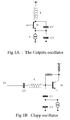
- FIG. 1A An example of a Colpitts oscillator is illustrated in figure 1A showing a transistor M biased by a current source I and associated with an inductance L and the series combination of C1 and C2 capacitors forming the parallel resonant tank circuit defining the oscillation frequency, in accordance with the formula.
- f 1 2 ⁇ L C 1 C 2 C 1 + C 2
- VFO variable frequency oscillator
- a variant of the Colpitts circuit, the well-known Clapp oscillator, avoids this problem by using two fixed capacitors C1 and C2, with a variable Capacitor which is arranged in series with the inductor, as shown in figure 2A , and which oscillates at the following frequency: f 1 2 ⁇ 1 L 1 C 0 + 1 C 1 + 1 C 2
- the Clapp oscillator is quite often used in association with a varactor, as illustrated in Figure 2 , which is based on a reversely biased diod forming the variable capacitor.
- variable frequency oscillator F
- VCO voltage controlled oscillator
- VFO variable frequency oscillator
- VCO voltage controlled oscillator
- VFO variable frequency oscillator
- VFO variable frequency oscillator
- variable Frequency oscillator comprising a first transistor and a second transistor, which may be for instance NPN transistors.
- the first transistor has a first terminal (e.g. collector) which is connected to a reference voltage, and a second terminal (e.g. emitter) which is connected to a first terminal of a first current source which second terminal is connected to ground.
- the first transistor further has a third terminal (e.g. base) which is connected to a first terminal of a first inductor and to a top terminal of a first capacitor C1 having a bottom terminal being connected to the first terminal of the first inductor and also to a top terminal of a second capacitor C2 having a bottom terminal being connected to ground.
- the second transistor has a first terminal (e.g. collector) which is connected to a reference voltage, and a second terminal (e.g. emitter) which is connected to a first terminal of a second current source which second terminal is connected to ground.
- the second transistor has a third terminal connected to a first terminal of a second inductor and to a top terminal of a third capacitor (C1), wherein the third capacitor has a bottom terminal which is connected to the first terminal of the second inductor and also to a top terminal of a fourth capacitor (C2) having a bottom terminal being connected to ground.
- variable frequency oscillator In order to achieve a variable frequency oscillation between the emitters (Outn , Outp) of the two transistors 10, 20, a variable tank capacitors is connected between the second terminal of inductors (14, 24), so as to form a circuit connecting in series all passive components composing the LC tank , thus masking most of parasitic capacitances. Consequently, the variable frequency oscillator may be used at a very high frequency.
- the circuit connecting the first and second inductors comprises two varactors connected in series with two capacitors so as to achieve analog control of the oscillation frequency.
- the varactors are sized so as to compensate temperature variation within the tuning range.
- the circuit connecting the first and second inductors comprises a bank of capacitors arranged in several paths connected in parallel , wherein each path comprises two capacitors connected in series with a switching component, wherein the switching components of all paths are controlled by means of a programmed tank Calibration Word (CW), so as to achieve the tuning of the oscillation frequency.
- CW programmed tank Calibration Word
- the bank of capacitors comprised within the circuit connecting the inductors is configured so as to allow coarse and fine digital control of the oscillation frequency.
- VFO variable frequency oscillator
- VCO voltage control oscillator
- figure 3 shows the arrangement with simplified biasing so as to focus on the main elements of the preferred embodiments.
- the architecture is based on a differential topology comprising a first transistor 10 and a second transistor 20 which, in the embodiment being considered are conventional NPN transistors.
- transistors 10 and 20 by other transistors, including FET transistors, MOS transistors etc...
- Transistor 10 has an emitter generating a first output signal Outp, a base and a collector.
- the collector of transistor 10 is connected to a reference voltage, serving as a ground for AC.
- the emitter of transistor 10 is connected to a first terminal of a first current source 13 having a second terminal connected to ground.
- the base of transistor 10 is connected to a first terminal of a first inductor 14, and also to the top terminal of a first capacitor 11, having a value of C1.
- Capacitor 11 has a bottom terminal which is connected to the first terminal of first inductor 14 and also to a top terminal of a second capacitor 12, having a value C2.
- Capacitor 12 has a bottom terminal which is connected to ground.
- transistor 20 is based on a Colpitts technology with a feedback network based on a third and a fourth capacitor, respectively of values C1 and C2. More particularly, the emitter of transistor 20 generates a second output signal Outn and is connected to a first terminal of a second current source 23 having a second terminal connected to ground.
- the base of transistor 20 is connected to a first terminal of a second inductor 24, and also to the top terminal of a third capacitor 21, having a value equal to C1.
- Capacitor 21 has a bottom terminal which is connected to the first terminal of second inductor 24 and also to a top terminal of a fourth capacitor 22, having a value C2.
- Capacitor 22 has a bottom terminal which is connected to ground.
- the feedback capacitors 12 and 22 have both their bottom terminal being connected to ground in order to isolate the two transistors 10 and 20.
- capacitors 12 and 22 (C2) were connected between the two emitters there would be a 2nd harmonic common mode oscillation building up that dominates over the differential fundamental one and might destroy the PN .
- first and second inductors 14 and 24 both have a second terminal which are connected via a circuit 100 achieving variable capacitance, so as to form a circuit connectina in memorizing the LC tank : capacitors 11, 12, 22, 21 and the two inductors 14 and 24.
- Circuit 100 allowing the connection in series of inductors 14 and 24 may take several forms.
- circuit 100 comprises two varactors 16 and 26 connected in series, with their two cathode terminal being connected together, and being further connected in series with two capacitors 15 and 25, so as to achieve a variable capacitance which can be used for performing a tuning of the oscillator.
- Control of the varactors can be achieved by applying a voltage control at the common cathode terminal of both varactors.
- the varactors are sized to compensate with its tuning range the temperature variation and assure that the VCO can lock to the programmed frequency and keep the lock over temperature if locked around a predefined voltage window. The voltage window will move according to the locking temperature.
- circuit 100 may further comprising a bank of capacitors tank arranged in several paths connected in parallel, respectively 101-102, 111-112, ..., 191-192, each individual path comprising two capacitors connected in series with a switching component.
- circuit 100 may comprise a first path comprising capacitors 101 and 102 connected in series with a first switching component 103.
- circuit 100 may comprise a second path comprising capacitors 111 and 112 connected in series with a second switching component 113.
- Figure 3 further illustrates a nth path comprising capacitors 191 and 192 connected series with a nth switching component 193...
- the bank of capacitors comprised within circuit 101 can be controlled by means of programmed tank Calibration Word (CW) which can be used for the purpose of independently controlling the switches 103, 113, ... 193... Thanks to such arranged, digital control of the frequency oscillation can be achieved.
- CW programmed tank Calibration Word
- the bank of capacitors forming the tank's capacitor bank of circuit 100 is made by a coarse and fine bank.
- the capacitors in the coarse and fine bank are of different type therefore an important overlap was considered between the coarse and fine range.
- the coarse bank is a 5bit binary weighted capacitive MIM bank (Metal Insulator Metal . «) whereas fine bank is a three bit binary weighted Metal Fringe bank (except for the lower frequency VCO where both banks are MIM).
- Control of the oscillation frequency can also be performed via an analog control, which can be done by applying a control voltage at the common cathode of varactors 16 and 26.
- the circuit of figure 3 is simplified and does not show all components that might be useful for the turning of the transistors. However, such components are well known to a skilled man and do not need any further development. It suffices to say that, in one embodiment, the bias current of both transistors is set by a resistor (not shown in figure 3 ) whose value can be programmed: the resistor value changes with the programmed tank Calibration Word (CW) applied for the control of switching elements 113, 123, ... 193, in order to keep the oscillation amplitude constant across the desired VCO digital tuning range.
- CW programmed tank Calibration Word
- the invention may be used for carrying out a VCO to be implemented in a Radio Frequency (RF) circuit of a communication apparatus.
- RF Radio Frequency
Landscapes
- Inductance-Capacitance Distribution Constants And Capacitance-Resistance Oscillators (AREA)
Priority Applications (3)
| Application Number | Priority Date | Filing Date | Title |
|---|---|---|---|
| EP16290005.4A EP3190706A1 (fr) | 2016-01-07 | 2016-01-07 | Oscillateur à fréquence variable ayant une large plage d'accord et un faible bruit de phase |
| EP17150384.0A EP3190707A1 (fr) | 2016-01-07 | 2017-01-05 | Oscillateur à fréquence variable ayant une large plage d'accord et un faible bruit de phase |
| US15/399,059 US10374549B2 (en) | 2016-01-07 | 2017-01-05 | Variable frequency oscillator having wide tuning range and low phase noise |
Applications Claiming Priority (1)
| Application Number | Priority Date | Filing Date | Title |
|---|---|---|---|
| EP16290005.4A EP3190706A1 (fr) | 2016-01-07 | 2016-01-07 | Oscillateur à fréquence variable ayant une large plage d'accord et un faible bruit de phase |
Publications (1)
| Publication Number | Publication Date |
|---|---|
| EP3190706A1 true EP3190706A1 (fr) | 2017-07-12 |
Family
ID=55272410
Family Applications (2)
| Application Number | Title | Priority Date | Filing Date |
|---|---|---|---|
| EP16290005.4A Withdrawn EP3190706A1 (fr) | 2016-01-07 | 2016-01-07 | Oscillateur à fréquence variable ayant une large plage d'accord et un faible bruit de phase |
| EP17150384.0A Withdrawn EP3190707A1 (fr) | 2016-01-07 | 2017-01-05 | Oscillateur à fréquence variable ayant une large plage d'accord et un faible bruit de phase |
Family Applications After (1)
| Application Number | Title | Priority Date | Filing Date |
|---|---|---|---|
| EP17150384.0A Withdrawn EP3190707A1 (fr) | 2016-01-07 | 2017-01-05 | Oscillateur à fréquence variable ayant une large plage d'accord et un faible bruit de phase |
Country Status (2)
| Country | Link |
|---|---|
| US (1) | US10374549B2 (fr) |
| EP (2) | EP3190706A1 (fr) |
Families Citing this family (2)
| Publication number | Priority date | Publication date | Assignee | Title |
|---|---|---|---|---|
| DE202016005441U1 (de) | 2016-09-07 | 2017-12-08 | l. G. Bauerhin GmbH | Fahrzeugsitz |
| CN112994617A (zh) * | 2021-04-13 | 2021-06-18 | 苏州英诺迅科技股份有限公司 | 一种改善频率温漂特性的振荡器电路结构 |
Citations (3)
| Publication number | Priority date | Publication date | Assignee | Title |
|---|---|---|---|---|
| US20110018642A1 (en) * | 2009-07-27 | 2011-01-27 | Broadcom Corporation | Differential varactor circuit for a voltage controlled oscillator |
| US20140347105A1 (en) * | 2013-05-23 | 2014-11-27 | Broadcom Corporation | Compensation of slow time-varying variations in voltage controlled oscillator (vco) frequency in cellular transceivers |
| US9209744B1 (en) * | 2013-02-13 | 2015-12-08 | M/A-Com Technology Solutions Holdings, Inc. | Laminate-based voltage-controlled oscillator |
Family Cites Families (3)
| Publication number | Priority date | Publication date | Assignee | Title |
|---|---|---|---|---|
| US6249190B1 (en) * | 1999-08-25 | 2001-06-19 | Conexant Systems, Inc. | Differential oscillator |
| US7289003B2 (en) * | 2005-08-03 | 2007-10-30 | Seiko Epson Corporation | Method and apparatus for amplitude control using dynamic biasing in a voltage controlled oscillator |
| US7791422B2 (en) * | 2007-10-17 | 2010-09-07 | Autoliv Asp, Inc. | Voltage controlled oscillator with cascaded emitter follower buffer stages |
-
2016
- 2016-01-07 EP EP16290005.4A patent/EP3190706A1/fr not_active Withdrawn
-
2017
- 2017-01-05 US US15/399,059 patent/US10374549B2/en not_active Expired - Fee Related
- 2017-01-05 EP EP17150384.0A patent/EP3190707A1/fr not_active Withdrawn
Patent Citations (3)
| Publication number | Priority date | Publication date | Assignee | Title |
|---|---|---|---|---|
| US20110018642A1 (en) * | 2009-07-27 | 2011-01-27 | Broadcom Corporation | Differential varactor circuit for a voltage controlled oscillator |
| US9209744B1 (en) * | 2013-02-13 | 2015-12-08 | M/A-Com Technology Solutions Holdings, Inc. | Laminate-based voltage-controlled oscillator |
| US20140347105A1 (en) * | 2013-05-23 | 2014-11-27 | Broadcom Corporation | Compensation of slow time-varying variations in voltage controlled oscillator (vco) frequency in cellular transceivers |
Non-Patent Citations (2)
| Title |
|---|
| SHENG-LYANG JANG ET AL: "A Differential Clapp-VCO in 0.13 $\mu{\rm m}$ CMOS Technology", IEEE MICROWAVE AND WIRELESS COMPONENTS LETTERS, IEEE SERVICE CENTER, NEW YORK, NY, US, vol. 19, no. 6, 1 June 2009 (2009-06-01), pages 404 - 406, XP011347550, ISSN: 1531-1309, DOI: 10.1109/LMWC.2009.2020040 * |
| SHENG-LYANG JANG ET AL: "A low voltage balanced Clapp VCO in 0.13 micromolar CMOS technology", vol. 52, no. 7, July 2010 (2010-07-01), XP002758995, ISSN: 0895-2477, Retrieved from the Internet <URL:http://onlinelibrary.wiley.com/doi/10.1002/mop.25275/pdf> [retrieved on 20160621] * |
Also Published As
| Publication number | Publication date |
|---|---|
| US20170201213A1 (en) | 2017-07-13 |
| EP3190707A1 (fr) | 2017-07-12 |
| US10374549B2 (en) | 2019-08-06 |
Similar Documents
| Publication | Publication Date | Title |
|---|---|---|
| EP0942531B1 (fr) | Circuit oscillateur en CMOS commandé en tension | |
| US5561398A (en) | LC-tuned voltage controlled ring oscillator | |
| US10454419B2 (en) | Hybrid resonator based voltage controlled oscillator (VCO) | |
| US8629732B2 (en) | Voltage-controlled oscillators and related systems | |
| KR100491280B1 (ko) | 멀티 단자형 mos 바랙터 | |
| US5187450A (en) | Voltage controlled oscillator suitable for complete implementation within a semiconductor integrated circuit | |
| US6657509B1 (en) | Differentially controlled varactor | |
| CN101682293A (zh) | 压控振荡器、以及使用其的锁相环电路和无线通信设备 | |
| US10833685B1 (en) | Linearized wide tuning range oscillator using magnetic balun/transformer | |
| US9660578B2 (en) | Electronic device with capacitor bank linearization and a linearization method | |
| US7064622B2 (en) | Dual differential LC voltage-controlled oscillator | |
| US5565821A (en) | Voltage controlled oscillator with improved tuning linearity | |
| US6927643B2 (en) | Oscillator topology for very low phase noise operation | |
| US7286024B2 (en) | Voltage-controlled oscillator with differential output | |
| EP2201686B1 (fr) | Oscillateur commandé par tension avec des étages de tampon émetteur-suiveur en cascade | |
| US7724102B2 (en) | Oscillator circuit | |
| US10374549B2 (en) | Variable frequency oscillator having wide tuning range and low phase noise | |
| US7019597B2 (en) | Method and circuitry for implementing a differentially tuned varactor-inductor oscillator | |
| US9099957B2 (en) | Voltage-controlled oscillators and related systems | |
| US10361657B2 (en) | Series of coupled synchronous oscillators | |
| US7411469B2 (en) | Circuit arrangement | |
| US6842081B2 (en) | Dual frequency voltage controlled oscillator circuit | |
| US20120235758A1 (en) | Voltage-controlled oscillators and related systems | |
| US7358825B2 (en) | Variable capacitance circuit arrangement | |
| US9673753B1 (en) | Voltage-controlled oscillator with improved tuning curve linearization |
Legal Events
| Date | Code | Title | Description |
|---|---|---|---|
| PUAI | Public reference made under article 153(3) epc to a published international application that has entered the european phase |
Free format text: ORIGINAL CODE: 0009012 |
|
| AK | Designated contracting states |
Kind code of ref document: A1 Designated state(s): AL AT BE BG CH CY CZ DE DK EE ES FI FR GB GR HR HU IE IS IT LI LT LU LV MC MK MT NL NO PL PT RO RS SE SI SK SM TR |
|
| AX | Request for extension of the european patent |
Extension state: BA ME |
|
| STAA | Information on the status of an ep patent application or granted ep patent |
Free format text: STATUS: THE APPLICATION IS DEEMED TO BE WITHDRAWN |
|
| 18D | Application deemed to be withdrawn |
Effective date: 20180113 |